

Page 1

PAMS Technical Documentation
RPM-1 Series Transceivers
Disassembly and
Troubleshooting
Issue 1 12/99 Nokia Mobile Phones Ltd.
Page 2
RPM-1
Disassembly and Troubleshooting
AMENDMENT RECORD SHEET
PAMS Technical Documentation
Amendment
Number
Date Inserted By Comments
12/99 OJuntune Original
Page 2
Nokia Mobile Phones Ltd.
Issue 1 12/99
Page 3

PAMS Technical Documentation
Disassembly and Troubleshooting
CONTENTS
Vocabulary 6. . . . . . . . . . . . . . . . . . . . . . . . . . . . . . . . . . . . . . . . . . . . .
Introduction 7. . . . . . . . . . . . . . . . . . . . . . . . . . . . . . . . . . . . . . . . . . . .
Disassembly 7. . . . . . . . . . . . . . . . . . . . . . . . . . . . . . . . . . . . . . . . . . .
Tools and Parts 7. . . . . . . . . . . . . . . . . . . . . . . . . . . . . . . . . . . . . .
Remove Antenna 8. . . . . . . . . . . . . . . . . . . . . . . . . . . . . . . . . . . . .
Open Top Cover Printed 8. . . . . . . . . . . . . . . . . . . . . . . . . . . . . . .
How to use the Opening Tool 9. . . . . . . . . . . . . . . . . . . . . . . .
Using Screwdriver as disassembly tool 10. . . . . . . . . . . . . . . .
Open Bottom Cover subassembly 11. . . . . . . . . . . . . . . . . . . . . .
Remove PCB from Extension Box subassembly 12. . . . . . . . . .
Reassembly 13. . . . . . . . . . . . . . . . . . . . . . . . . . . . . . . . . . . . . . . . . . . .
RPM-1
Page No
Install the PCB to Extension Box subassembly 13. . . . . . . . .
Assemble Bottom Cover subassembly 14. . . . . . . . . . . . . . . . . .
Close Top Cover Printed 14. . . . . . . . . . . . . . . . . . . . . . . . . . . .
Push Antenna into the Extension Box subassembly 15. . . . . . .
Baseband Troubleshooting 16. . . . . . . . . . . . . . . . . . . . . . . . . . . . . . .
Current Consumption in Fault Diagnostics 16. . . . . . . . . . . . . . .
Card Phone does not Communicate with the Host Computer 17
MCU Problems 18. . . . . . . . . . . . . . . . . . . . . . . . . . . . . . . . . . . . . . .
Flasah Programming Initialization sequence 19. . . . . . . . . . .
WinTesla Self Tests 19. . . . . . . . . . . . . . . . . . . . . . . . . . . . . . . . . . .
ADC Readings With WinTesla 20. . . . . . . . . . . . . . . . . . . . . . .
SIM Card Failure 21. . . . . . . . . . . . . . . . . . . . . . . . . . . . . . . . . . . . .
SIM interface diagram 22. . . . . . . . . . . . . . . . . . . . . . . . . . . . . .
SIM Card Reader pins 22. . . . . . . . . . . . . . . . . . . . . . . . . . . . . .
Audio Fails 23. . . . . . . . . . . . . . . . . . . . . . . . . . . . . . . . . . . . . . . . . .
RF Troubleshooting 24. . . . . . . . . . . . . . . . . . . . . . . . . . . . . . . . . . . . .
RF trouble shooting principles 24. . . . . . . . . . . . . . . . . . . . . . . . . .
Quick check RX with WinTesla 26. . . . . . . . . . . . . . . . . . . . . . . . . . . .
Gather test equipment 26. . . . . . . . . . . . . . . . . . . . . . . . . . . . . . . .
Connect test equipment 26. . . . . . . . . . . . . . . . . . . . . . . . . . . . . . .
Settings and diagnostic 26. . . . . . . . . . . . . . . . . . . . . . . . . . . . . . . .
Quick check TX with WinTesla 27. . . . . . . . . . . . . . . . . . . . . . . . . . . .
Test equipment list 27. . . . . . . . . . . . . . . . . . . . . . . . . . . . . . . . . . . .
Connect test equipment 27. . . . . . . . . . . . . . . . . . . . . . . . . . . . . . .
Settings & diagnostic 27. . . . . . . . . . . . . . . . . . . . . . . . . . . . . . . . . .
GSM 28. . . . . . . . . . . . . . . . . . . . . . . . . . . . . . . . . . . . . . . . . . . . .
PCN 28. . . . . . . . . . . . . . . . . . . . . . . . . . . . . . . . . . . . . . . . . . . . . .
RX trouble shooting 29. . . . . . . . . . . . . . . . . . . . . . . . . . . . . . . . . . . . .
Issue 1 12/99
Nokia Mobile Phones Ltd.
Page 3
Page 4

RPM-1
Disassembly and Troubleshooting
Test equipment 29. . . . . . . . . . . . . . . . . . . . . . . . . . . . . . . . . . . . . . .
GSM Receiver 30. . . . . . . . . . . . . . . . . . . . . . . . . . . . . . . . . . . . . . .
Settings 30. . . . . . . . . . . . . . . . . . . . . . . . . . . . . . . . . . . . . . . . . . .
Test diplexer 30. . . . . . . . . . . . . . . . . . . . . . . . . . . . . . . . . . . . . . .
Test RX duplex filter 30. . . . . . . . . . . . . . . . . . . . . . . . . . . . . . . .
Test LNA (CRFU3 asic) 30. . . . . . . . . . . . . . . . . . . . . . . . . . . . .
Test RX SAW filter 31. . . . . . . . . . . . . . . . . . . . . . . . . . . . . . . . . .
Test UHF mixer 31. . . . . . . . . . . . . . . . . . . . . . . . . . . . . . . . . . . .
Test 73MHz filter 31. . . . . . . . . . . . . . . . . . . . . . . . . . . . . . . . . . .
Test SUMMA asic 31. . . . . . . . . . . . . . . . . . . . . . . . . . . . . . . . . .
PCN Receiver 33. . . . . . . . . . . . . . . . . . . . . . . . . . . . . . . . . . . . . . . .
Settings 33. . . . . . . . . . . . . . . . . . . . . . . . . . . . . . . . . . . . . . . . . . .
Test diplexer 33. . . . . . . . . . . . . . . . . . . . . . . . . . . . . . . . . . . . . . .
Test rx/tx switch 33. . . . . . . . . . . . . . . . . . . . . . . . . . . . . . . . . . . .
Test pre_LNA rx filter 33. . . . . . . . . . . . . . . . . . . . . . . . . . . . . . .
Test LNA 33. . . . . . . . . . . . . . . . . . . . . . . . . . . . . . . . . . . . . . . . . .
Test RX RF SAW filter 34. . . . . . . . . . . . . . . . . . . . . . . . . . . . . .
Test UHF mixer 34. . . . . . . . . . . . . . . . . . . . . . . . . . . . . . . . . . . .
Test VHF mixer 34. . . . . . . . . . . . . . . . . . . . . . . . . . . . . . . . . . . .
Test 73MHz filter 34. . . . . . . . . . . . . . . . . . . . . . . . . . . . . . . . . . .
Test Summa asic 35. . . . . . . . . . . . . . . . . . . . . . . . . . . . . . . . . . .
PAMS Technical Documentation
TX trouble shooting 37. . . . . . . . . . . . . . . . . . . . . . . . . . . . . . . . . . . . .
Test equipment 37. . . . . . . . . . . . . . . . . . . . . . . . . . . . . . . . . . . . . . .
GSM TX 38. . . . . . . . . . . . . . . . . . . . . . . . . . . . . . . . . . . . . . . . . . . . .
Settings 38. . . . . . . . . . . . . . . . . . . . . . . . . . . . . . . . . . . . . . . . . . .
Test SUMMA TX part 38. . . . . . . . . . . . . . . . . . . . . . . . . . . . . . .
Test CRFU3 TX part 41. . . . . . . . . . . . . . . . . . . . . . . . . . . . . . . .
Test TX RF SAW filter 42. . . . . . . . . . . . . . . . . . . . . . . . . . . . . . .
Test power control circuit 42. . . . . . . . . . . . . . . . . . . . . . . . . . . .
Test power amplifier 43. . . . . . . . . . . . . . . . . . . . . . . . . . . . . . . .
Test duplexer TX side 44. . . . . . . . . . . . . . . . . . . . . . . . . . . . . . .
Test diplexer GSM side 44. . . . . . . . . . . . . . . . . . . . . . . . . . . . .
GSM1800 TX 45. . . . . . . . . . . . . . . . . . . . . . . . . . . . . . . . . . . . . . . .
Settings 45. . . . . . . . . . . . . . . . . . . . . . . . . . . . . . . . . . . . . . . . . . .
Test SUMMA TX part 45. . . . . . . . . . . . . . . . . . . . . . . . . . . . . . .
Test CRFU3 TX part 46. . . . . . . . . . . . . . . . . . . . . . . . . . . . . . . .
Test 1st TX RF SAW filter 46. . . . . . . . . . . . . . . . . . . . . . . . . . .
Test buffer amplifier 46. . . . . . . . . . . . . . . . . . . . . . . . . . . . . . . .
Test 2nd TX RF SAW filter 47. . . . . . . . . . . . . . . . . . . . . . . . . . .
Test power control circuit 47. . . . . . . . . . . . . . . . . . . . . . . . . . . .
Test power amplifier 47. . . . . . . . . . . . . . . . . . . . . . . . . . . . . . . .
Test RX / TX switch 49. . . . . . . . . . . . . . . . . . . . . . . . . . . . . . . . .
Test diplexer GSM1800 side 49. . . . . . . . . . . . . . . . . . . . . . . . .
Synthesizer Troubleshooting 50. . . . . . . . . . . . . . . . . . . . . . . . . . . . .
Test equipment 50. . . . . . . . . . . . . . . . . . . . . . . . . . . . . . . . . . . . . . .
Page 4
Nokia Mobile Phones Ltd.
Issue 1 12/99
Page 5

PAMS Technical Documentation
Settings 51. . . . . . . . . . . . . . . . . . . . . . . . . . . . . . . . . . . . . . . . . . . . .
VCTCXO (G802) 51. . . . . . . . . . . . . . . . . . . . . . . . . . . . . . . . . . .
UHF VCO (G801) 52. . . . . . . . . . . . . . . . . . . . . . . . . . . . . . . . . .
VHF VCO (G803) 53. . . . . . . . . . . . . . . . . . . . . . . . . . . . . . . . . .
PLL IC (N800) 54. . . . . . . . . . . . . . . . . . . . . . . . . . . . . . . . . . . . .
13 Mhz buffer 54. . . . . . . . . . . . . . . . . . . . . . . . . . . . . . . . . . . . . .
Repair instructions 55. . . . . . . . . . . . . . . . . . . . . . . . . . . . . . . . . . . .
RF–BB Interface 56. . . . . . . . . . . . . . . . . . . . . . . . . . . . . . . . . . . . .
Test Points of GX9 57. . . . . . . . . . . . . . . . . . . . . . . . . . . . . . . . . . . .
Test Points, Top side 59. . . . . . . . . . . . . . . . . . . . . . . . . . . . . . . .
Test Points, Bottom side 60. . . . . . . . . . . . . . . . . . . . . . . . . . . .
Disassembly and Troubleshooting
RPM-1
Issue 1 12/99
Nokia Mobile Phones Ltd.
Page 5
Page 6

RPM-1
Disassembly and Troubleshooting
Vocabulary
ASIC Application Specific Integrated Citcuit
BB Baseband part of RPM–1
CCONT Power supply ASIC of RPM–1
CIS Card Information Structure specified by PC Card
standard. Stored in EEPROM in RPM–1
COBBA_GJP Audio codec and RF interface ASIC of RPM–1
DSP Digital Signal Processor
EEPROM Elecrically Erasable Programmable Read Only
Memory
Flash Reprogrammable non–volatile memory
GX9 Tranceiver module of RPM–1
HSCSD High Speed Circuit Switched Data
(multislot GSM transmission)
HW Hard Ware
MAD MCU + ASIC + DSP
MAD2WD1 Version of MAD2 ASIC used in RPM–1
MCU MicroController Unit
PCB Printed Circuit Board
PURX Power Up Reset, active low. Reset signal to
MAD2WD1
RPM–1 Type designation of Nokia Cellular Card Phone V.2
Sulo PC Card interface ASIC of RPM–1
PAMS Technical Documentation
Page 6
Nokia Mobile Phones Ltd.
Issue 1 12/99
Page 7
PAMS Technical Documentation
Introduction
The purpose of this document is to help in hardware troubleshooting of
the RPM–1, Nokia Cellular Card Phone V.2. RPM–1 is a GSM900/1800
HSCSD PC Card.
Disassembly
Tools and Parts
RPM-1
Disassembly and Troubleshooting
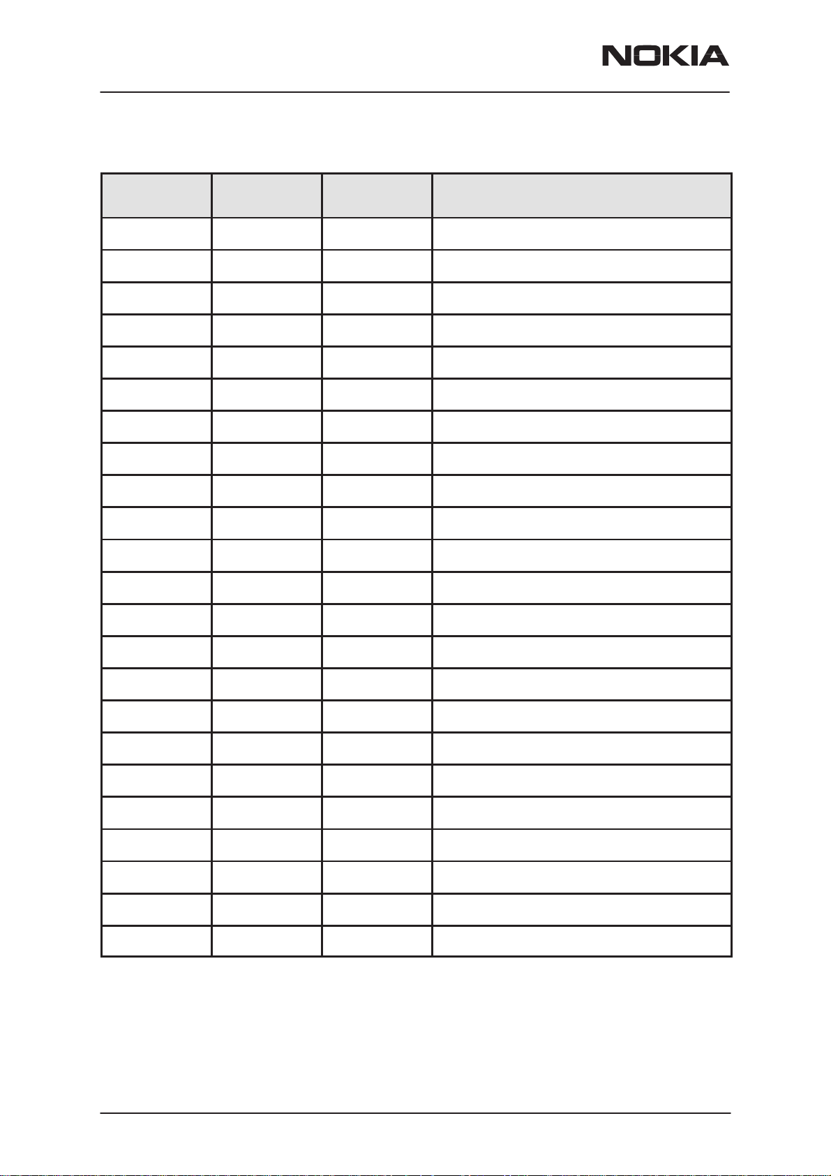
Fig. 1 Disassembled parts, left to right:
0660200 Antenna
9507011 Top Cover Printed
9507010 Bottom Cover subassembly
9477002 Extension Box subassembly
GX9 module (PCB with components)
Tools:
Opening tool for the RPM-1 Phone
Screwdriver
Issue 1 12/99
Nokia Mobile Phones Ltd.
Page 7
Page 8
RPM-1
Disassembly and Troubleshooting
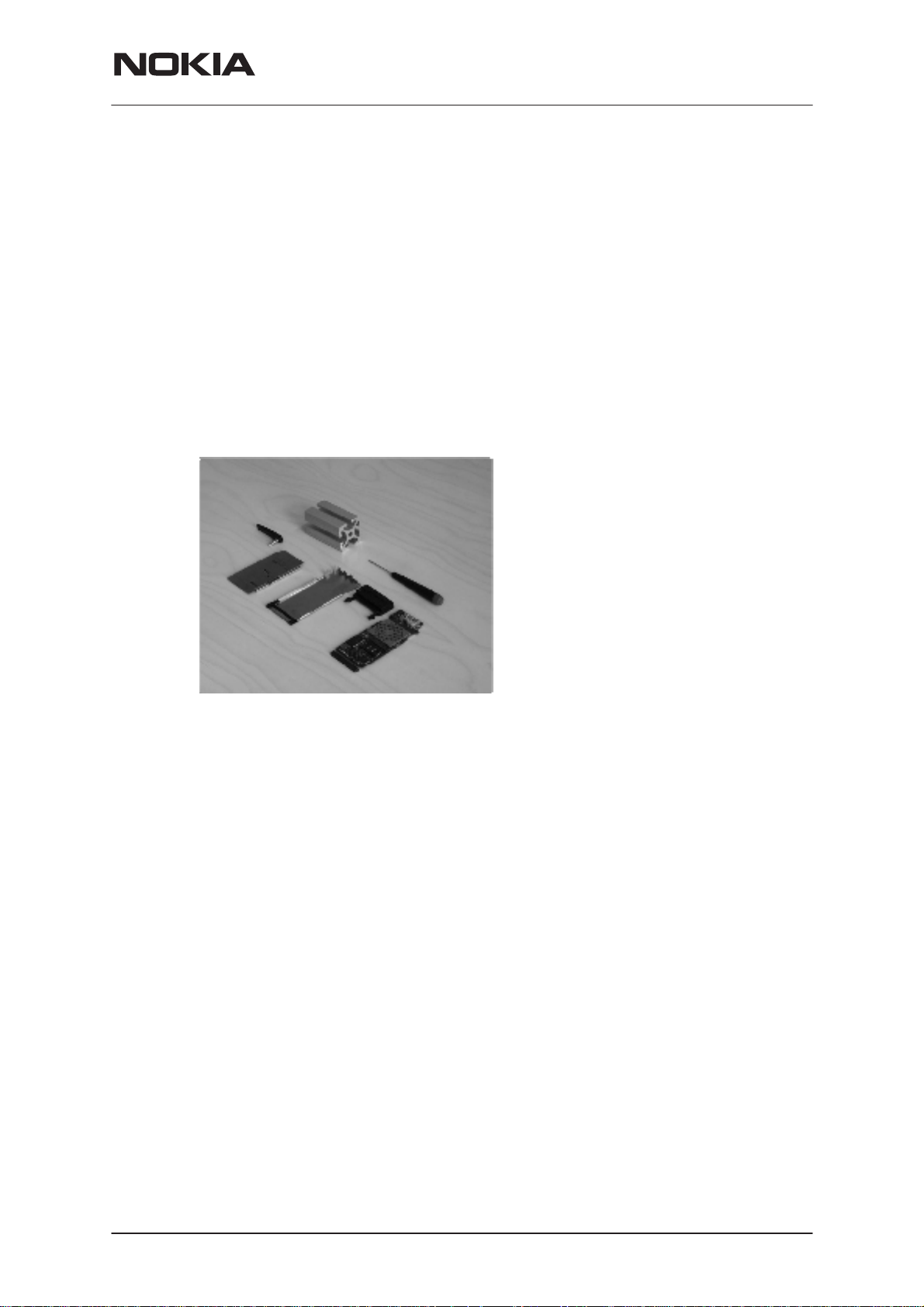
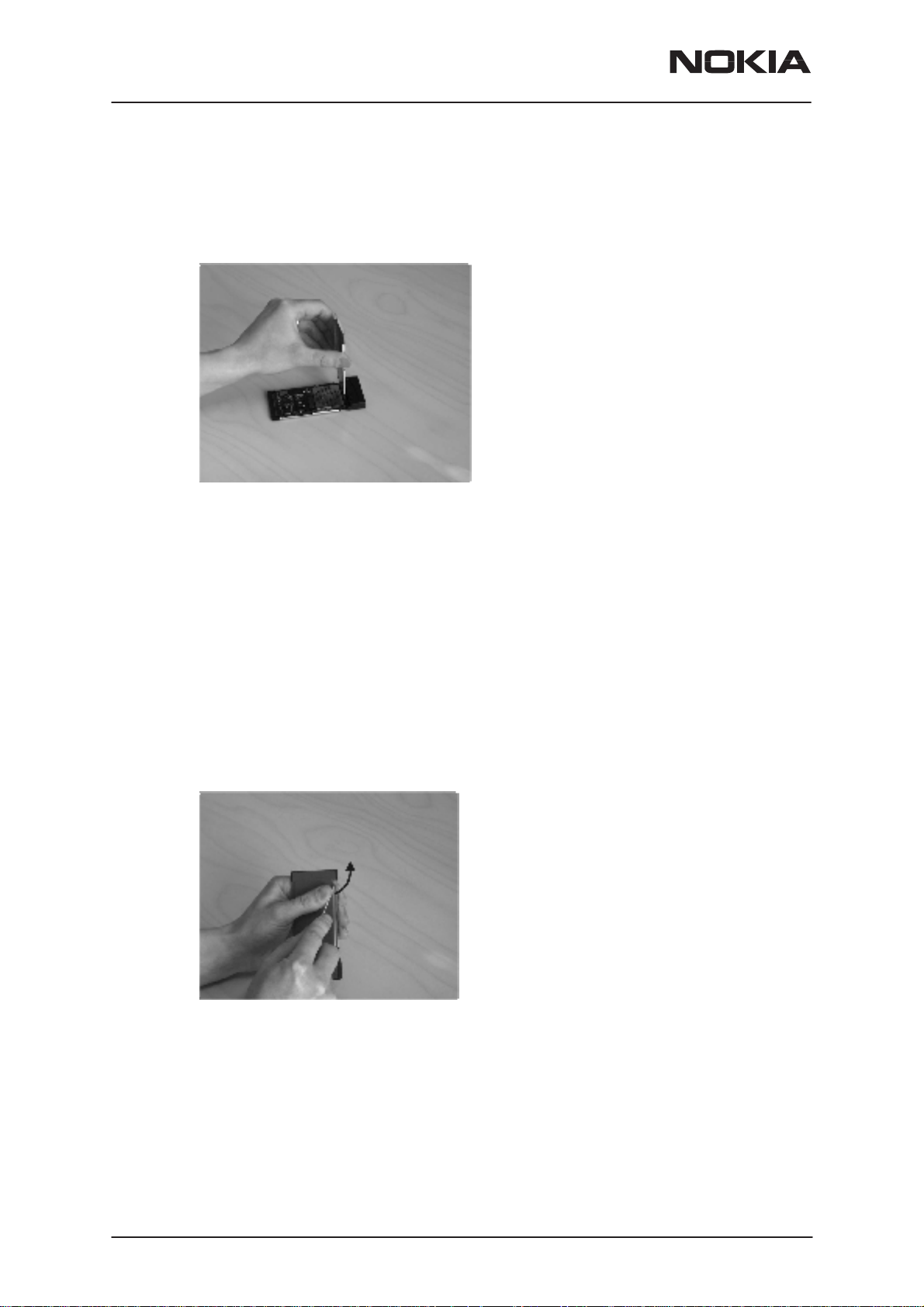
Remove Antenna
Pull Antenna smoothly from the Extension Box subassembly.
Refer to the picture below.
PAMS Technical Documentation
Fig 2. Note:
Do not bend the antenna.
Open Top Cover Printed
Use preferably the opening tool as you open the Top Cover Printed.
Please note that It is easy to damage covers with a screwdriver.
Note: (general)
Do not open Top Cover Printed from left side (top view). Flash component
may damage on the PCB.
Open Top Cover Printed only from right side (top view). See picture 3.
Page 8
Fig 3. Top view
Nokia Mobile Phones Ltd.
Issue 1 12/99
Page 9
PAMS Technical Documentation
How to use the Opening Tool
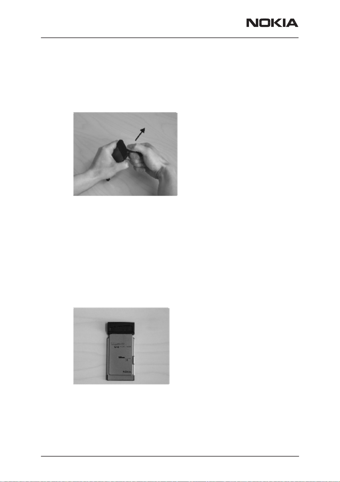
STEP 1:
Put the sharp edge of the opening tool to the Top Cover Printed’s edge
and turn the opening tool smoothly. See picture 4.
RPM-1
Disassembly and Troubleshooting
Fig.4. Position of the opening tool
STEP 2:
Release the right side of the RPM-1 .
Push Top Cover Printed a little bit to left side after you have opened the
right side of the RPM-1 .
Open carefully the Top Cover Printed simultaneously pushing the Top
Cover Printed to left side .
See picture 5.
Fig. 5. Open Top Cover Printed
Issue 1 12/99
Nokia Mobile Phones Ltd.
Page 9
Page 10
RPM-1
Disassembly and Troubleshooting
STEP 3:
Lift Top Cover Printed. Top Cover Printed must be about 90 degree open.
See picture 6 below.
Fig.6. Lift Top Cover Printed
PAMS Technical Documentation
Using Screwdriver as disassembly tool
Use preferably the opening tool as you open the Top Cover Printed.
Please note that It is easy to damage the covers and the electronics, too,
using a screwdriver.
STEP 1:
Put the screwdriver to the edge of the Top Cover Printed.
Push the Top Cover Printed’s edge over the edge of the Bottom Cover
subassembly.
See picture 7.
Page 10
Fig. 7. Position of the screwdriver
STEP 2:
Release left side of the RPM-1 .
Push Top Cover Printed a little bit to left side after you have opened right
side of the RPM-1 .
Open carefully Top Cover Printed same time as you push Top Cover
Printed to left side .
Nokia Mobile Phones Ltd.
Issue 1 12/99
Page 11
PAMS Technical Documentation
See picture 5.
STEP 3:
Lift Top Cover Printed. Top Cover Printed must be 90 degree open. See
picture 6.
Note when using a screwdriver:
Avoid scratching covers
Do not push screwdriver too much inside the RPM-1. Only a few mm is
allowed.
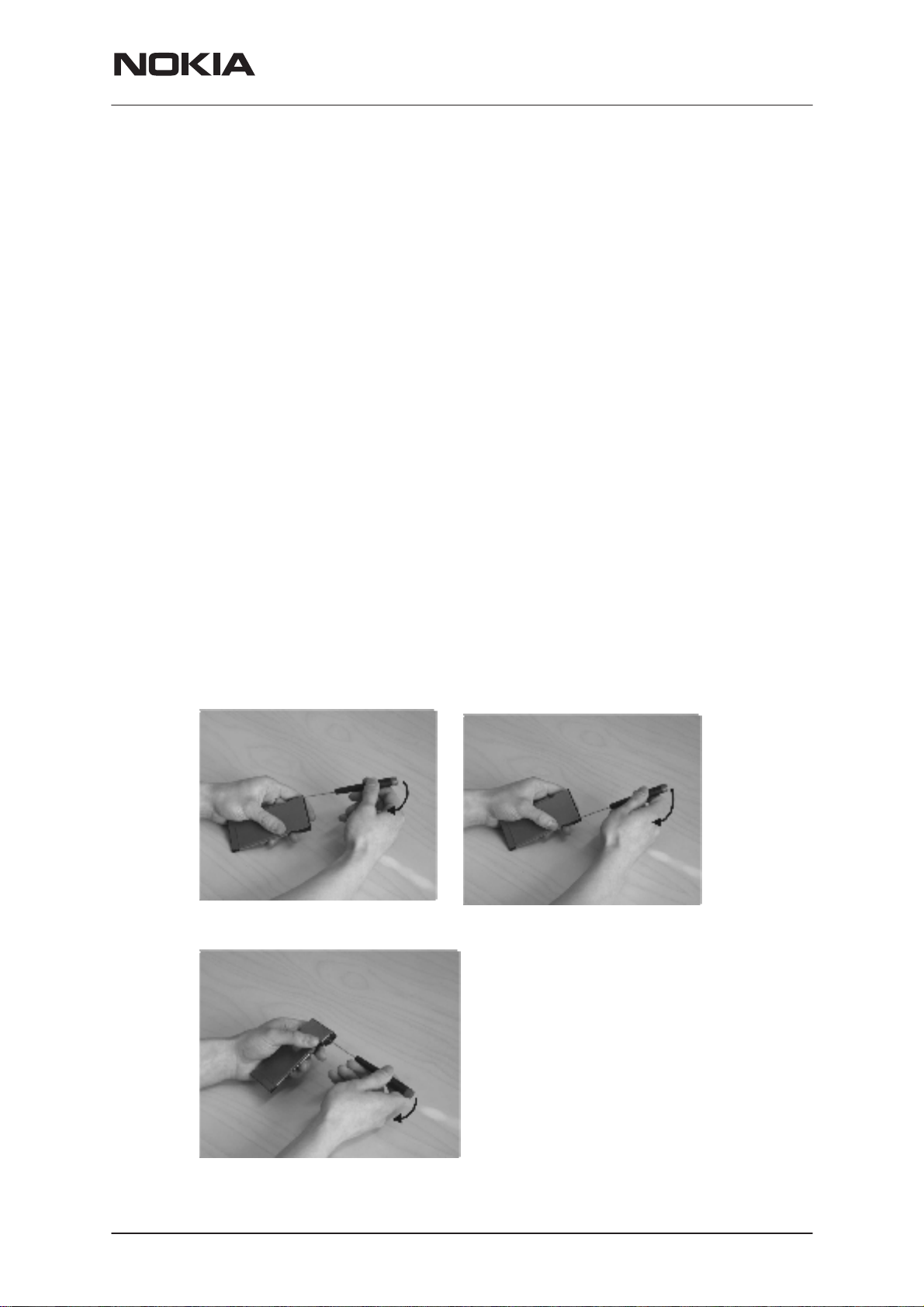
Open Bottom Cover subassembly
Use screwdriver as you open the Bottom Cover subassembly.
Note: (general)
Do not push screwdriver too much inside to Extension Box subassembly.
Only a few mm is allowed.
RPM-1
Disassembly and Troubleshooting
STEP 1:
Push screwdriver (use standard screwdriver ~∅ 1,50 mm) to gap be-
tween Extension Box subassembly and Bottom Cover subassembly (left
or right side).
Open Bottom Cover subassembly step by step as illustrated in pictures 8
to 9.
Fig. 8 : Open Bottom Cover subassembly
Fig 9. Open Bottom Cover subassembly
Issue 1 12/99
Nokia Mobile Phones Ltd.
Page 11
Page 12
RPM-1
Disassembly and Troubleshooting
STEP 2:
–Lift Bottom Cover subassembly. See picture 10.
Fig. 10. Lift
PAMS Technical Documentation
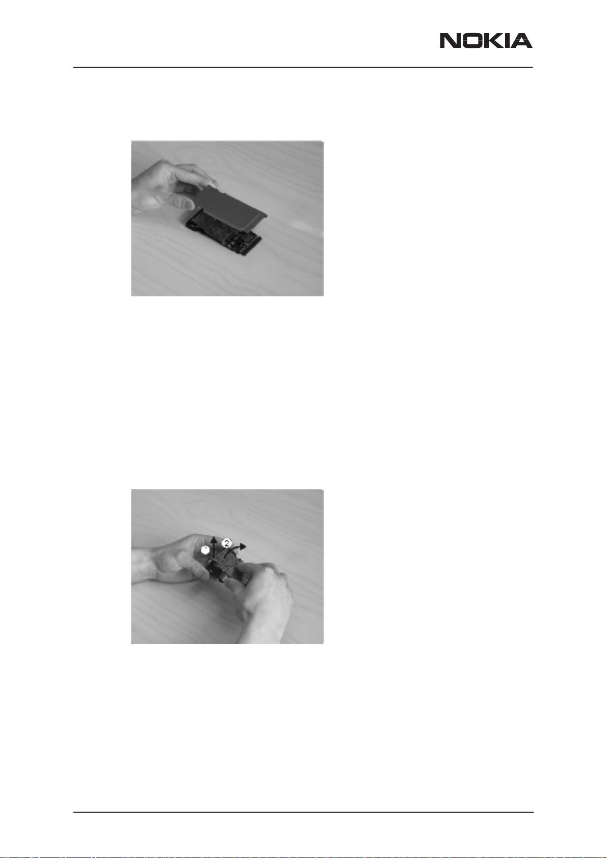
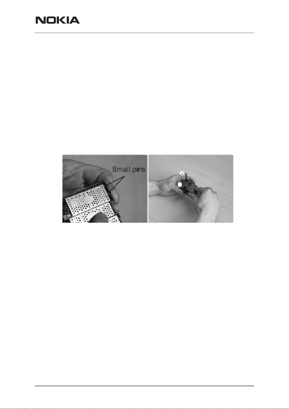
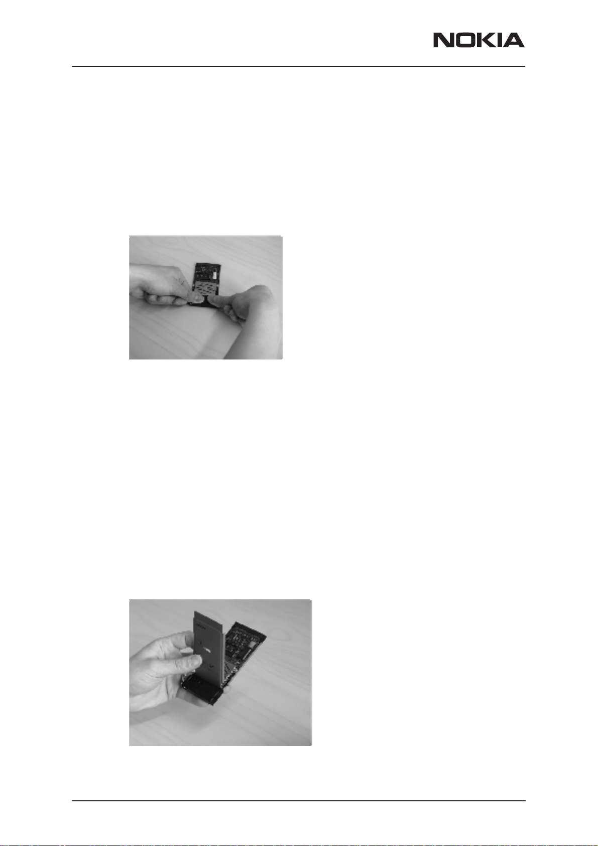
Remove PCB from Extension Box subassembly
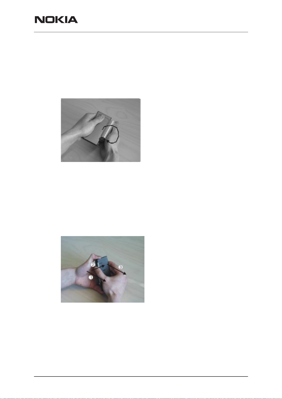
STEP 1:
–Lift and turn the GX9 to audio connector’s side and snap fit between Ex-
tension Box subassembly and GX9 will disengage.
Small pins near the audio connector will damage the GX9 if the module is
lifted in vertical direction.
The angle for turn is about 30 degree. Pull the GX9 smoothly from under
small pins. See picture 11.
Page 12
Fig. 11. Lift and turn
Note:
–Take extra care when performing this operation. Do not use too much
force, the PCB may break.
Nokia Mobile Phones Ltd.
Issue 1 12/99
Page 13
PAMS Technical Documentation
Reassembly
Install the PCB to Extension Box subassembly
STEP 1:
–Slide carefully the GX9 under the Extension Box subassembly’s small
pins near audio connector.
–Turn and push the GX9 into the Extension Box subassembly after GX9 in
assembled under small pins.
–Assembly is OK as the snap fit between these parts engages. The as-
sembly angle for turn is about 30 degree. See picture 12.
RPM-1
Disassembly and Troubleshooting
Fig. 12. Slide and turn
Note:
–Do not use old Extension Box subassembly for assembly. Antenna con-
tact between Bottom Cover subassembly and Antenna insert may disengage.
–Use only new (unused) Extension Box subassembly.
–Do not bend audio connector springs as you assembled GX9. Be very
careful with the audio connector springs. Change audio connector if needed.
Issue 1 12/99
Nokia Mobile Phones Ltd.
Page 13
Page 14
RPM-1
Disassembly and Troubleshooting
Assemble Bottom Cover subassembly to the Extension Box subassembly
STEP 1:
–Put Extension Box subassembly on the Bottom Cover subassembly and
push it against table, etc. Push only from the Extension Box subassembly.
See picture 13.
PAMS Technical Documentation
Fig. 13. Push from the Extension Box subassembly
Note:
–Check the dimensions of the Bottom Cover subassembly grounding clips
before assembly. Dimension must be 1,80 +0,2 mm. Change the clips’
dimension into tolerance range if needed.
Clip is situated in the right side of the Bottom Cover subassembly (top
view).
Close Top Cover Printed
STEP 1:
Assemble Top Cover Printed to the holes of the Extension Box subassem-
bly. See picture 14.
Page 14
Fig. 14. Assembly angle
Nokia Mobile Phones Ltd.
Issue 1 12/99
Page 15
PAMS Technical Documentation
STEP 2:
First assemble the left side of the RPM-1. It’s important to start assembly
near Extension Box subassembly. Do not push near flash component.
See picture 15.
RPM-1
Disassembly and Troubleshooting
Fig. 15. Close left side
STEP 3:
Assemble the right side as the left side was assembled. Start assembly
near Extension Box subassembly. See picture 16.
Fig. 16. Close right side
Push Antenna into the Extension Box subassembly
STEP 1:
–Push the Antenna smoothly to Extension Box subassembly
Issue 1 12/99
Nokia Mobile Phones Ltd.
Page 15
Page 16

RPM-1
Disassembly and Troubleshooting
PAMS Technical Documentation
Baseband Troubleshooting
When a faulty RPM-1 is taken under investigation a first a thorough visual
inspection should be done. Special attention should be paid to
– Solderings and condition of PCMCIA connector X400,
– Solderings of Sulo ASIC D400,
– Alignment of BGA packaged ICs MAD2WD1, CCONT, COBBA and
Flash (D500, N700, N600 and D501 respectively)
Current Consumption in Fault Diagnostics
When the RPM-1 is placed in service adapter JBS–23 and RESET button
is being pressed , the current consumption should be around 30 mA..
If the current consumption of the RPM-1 is several hundred mAs even
when RESET button of service adapter is pressed, there is obviously a
short circuit in the main power supply rail or massive failure in one of the
following circuits: CCONT (N700), PA power switch (N701), Sulo (D400),
Sulo core voltage regulator (N400) or MBUS switch (D402). Check
PCMCIA supply voltage (VCC) resistance to ground to determine this.
If the current consumption of the RPM-1 is constantly significantly higher
than expected, for example 100–300 mA even when RESET button of
service adapter is pressed, but VCC to GND resistance is OK, either one
of CCONT’s (N700) regulator outputs is short circuited to GND or Sulo
core voltage regulator (N400) output is short circuited to GND. Check resistances to GND from CCONT regulator output voltages. (J702, J703,
J704, J705, J706, J708, J724 to be 2.8 V, J712 to be either 1.975 or 1.75
V and J709 to be 5 V.) Also check Sulo core voltage regulator output voltage to be 2.8 V. (This can be measured from capacitor C404’s positive
terminal.)
Page 16
Nokia Mobile Phones Ltd.
Issue 1 12/99
Page 17
PAMS Technical Documentation
Disassembly and Troubleshooting
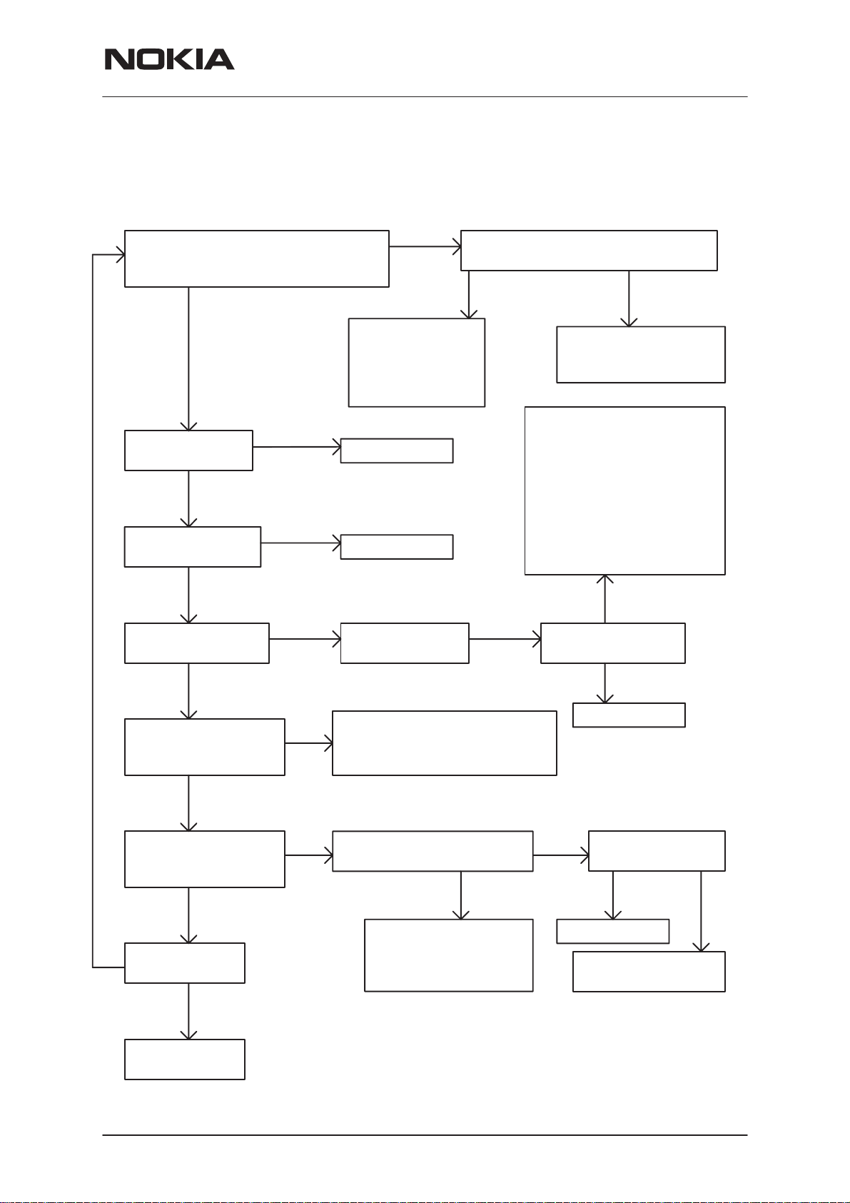
Card Phone does not Communicate with the Host Computer
RPM-1
Does laptop recognize the card
as Nokia Cellular Card Phone when
inserted to PC Card slot?
No
Check PCMCIA
connector X400
OK
Check Sulo ASIC
D400 solderings
OK
Check Vsulo level
2.8 V in C404
Fail
Fail
Fail
Yes
Probably a
problem with
MAD2WD1 ASIC.
Go to
MCU Problems
Repair X400
Repair D400
Check if Vsulo
is short circuited
PC Card interface is OK. Initiate
WinTesla connection with JBS–23
Phone not found
MAD2WD1 is
on line and working
Go to WinTesla self tests
Card power supply
fails. Check supply
voltage, check VCC
current consumption
during RESET, check
VCC line for possible
short circuits. If supply
is OK, problem is either
X400, D400, D402, N400,
N700, N701, N200 or N201
Not
5V
No Check Vsulo input
voltage VCC
WT conn.
can be created
OK
Check 32 kHz clock
J701. Square vawe,
VPP ~2.8 V
OK
Check 13 MHz clock
R411, sine vawe,
VPP> 0.5 V
OK
Reprogram CIS
OK
EEPROM
FAIL
Check X400
D400 and D401
Fail
Fail
Check VCC supply, N700,
B700+surroundings. Probably
N700 or B700 failure.
Check VCTCXO output,
13 MHz should be in R818
OK
Faiure in V800, R816,
R817, R819, C402 or
R411, or RFC signal
is short circuited
5V
Change N400
Fail
Check VXO level
2.8V in C836
OK Fail
Change G802
Shot circuit in VXO
line or N700 failure
Issue 1 12/99
Nokia Mobile Phones Ltd.
Page 17
Page 18
RPM-1
Disassembly and Troubleshooting
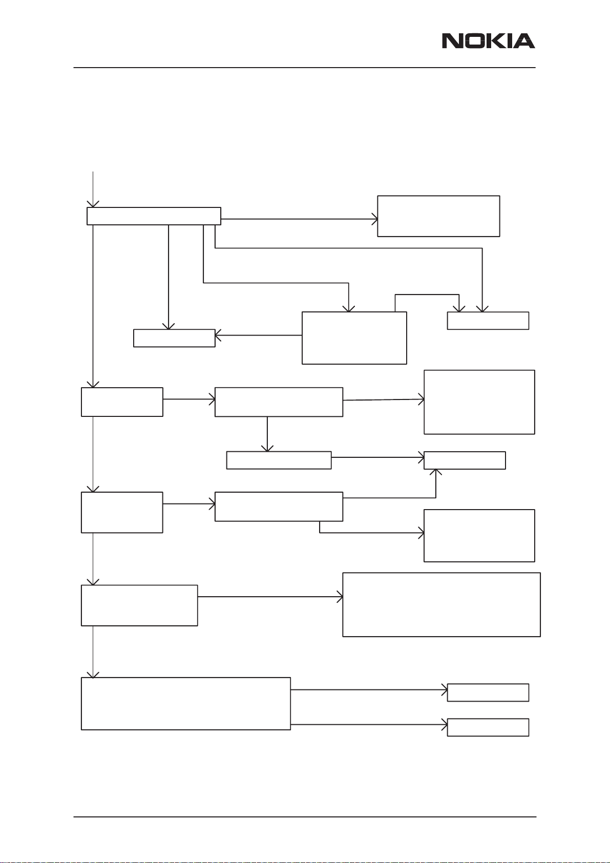
MCU Problems
Host computer recognizes
card as Nokia Cellular Card Phone
Try Reflashing the Card Flashing is succesful
ERROR15
PAMS Technical Documentation
If WT connection still
cannot be initialized.
change D500
MCU Boot
failure 01
Change D500
Check VBB
2.8 V in C717
OK
Check V2V
1.98 or 1.75 V
in J712
OK
MCU Boot
failure 02–04
Fail
Fail
Check VBB power net
for short circuits
Check V2V power net
for short circuits
MCU Boot failure 05
No cracs
in D501
OK
Check N700, L700
D500 or D501
failure. Visually
inspect D501 for
microscopic cracs.
Short circuit
Visually OK
OK
Short circuit
Cracs in
D501
Change D501
Try and identify
SC cause. Possible
places are: D500,
D501, D502, N600
N700, V703
Change N700
Try and identify
SC cause. Possible
places are: D500
and N700
Check that
PURX goes high
after power up. J503
OK
Check that after FBUS TX (J413) transition
from HI to LO, MBUS (J502) goes from
LO to HI. (See Flash Programming initiation
sequence picture below.)
Page 18
PURX stays low
Nokia Mobile Phones Ltd.
If laptop recognizes Cellular Card
Phone When inserted to PC Card
slot, but PURX J503 stays low
when phone is in JBS–23, check
R502 and D400. If OK, change D400
MBUS (J502) always high
FBUS TX (J413) always low
Change D402
Change D500
Issue 1 12/99
Page 19

PAMS Technical Documentation
Disassembly and Troubleshooting
Flasah Programming Initialization sequence
RPM-1
PURX to MAD2WD1 (J503)
(Actually transition is slower)
Flash clock to MAD2WD1
(MBUS, J502)
Flash data to MAD2WD1
(MAD FBUS RX, J410)
Flash ACK from MAD2WD1
(MAD FBUS TX, J413)
WinTesla Self Tests
Open product RPM–1 in WinTesla and go to Testing ––> Self tests...
menu .
If no tests are reported as FAIL, powering, clocking and digital parts of
base band are OK.
See list below of what to do in case of different self test failures:
– MCU ROM Checksum FAIL:
Reflash card phone.
still fails: total erase flash, reflash phone, run all factory setups, retune
RF, rebuild IMEI and open SIM locks.
still fails: change flash IC (D501), reflash phone, run all factory setups,
retune RF, rebuild IMEI and open SIM locks.
still fails: change MAD2WD1 (D500).
– MCU RAM Interface FAIL:
Reflash card phone,
still fails: change MAD2WD1 (D500),
still fails: change flash IC (D501), reflash phone, run all factory setups,
retune RF, rebuild IMEI and open SIM locks
– MCU EEPROM Interface FAIL:
Reflash card phone, run factory setup.
still fails: total erase flash, reflash phone, run all factory setups, retune
RF, rebuild IMEI and open SIM locks.
Issue 1 12/99
Nokia Mobile Phones Ltd.
Page 19
Page 20

RPM-1
Disassembly and Troubleshooting
– CCONT Interface FAIL:
MAD2WD1 (D500) or CCONT (N700) or traces connecting them are
faulty.
– Security Data Fail:
Reflash card phone
still fails: total erase flash, reflash phone, run all factory setups, retune
RF, rebuild IMEI and open SIM locks.
still fails: change flash IC (D501), reflash phone, run all factory setups,
retune RF, rebuild IMEI and open SIM locks.
– EEPROM Tune Checksum FAIL :
Reflash card phone,
still fails: Run factory setups, check RF tunings.
still fails: total erase flash, reflash phone, run all factory setups, retune
RF, rebuild IMEI and open SIM locks.
still fails: change flash IC (D501), reflash phone, run all factory setups,
retune RF, rebuild IMEI and open SIM locks.
PAMS Technical Documentation
– MCU Download DSP FAIL:
Reflash card phone,
still fails: change MAD2WD1 (D500)
– DSP Alive FAIL:
Reflash card phone,
still fails: change MAD2WD1 (D500)
– COBBA Serial/Parallel FAIL:
MAD2WD1 (D500) or COBBA (N600) or traces connecting them are
faulty.
– EEPROM Sec Checksum FAIL:
Reflash card phone
still fails: total erase flash, reflash phone, run all factory setups, retune
RF, rebuild IMEI and open SIM locks.
still fails: change flash IC (D501), reflash phone, run all factory setups,
retune RF, rebuild IMEI and open SIM locks.
ADC Readings With WinTesla
Select Testing ––> ADC Readings
Battery voltage should be about 5.0 V, if not, there is probably a problem
with either power supply, CCONT (N700) or MAD2WD1 – CCONT interface. First try running factory setup. (Check RF tunings after running factory setup!)
Page 20
Battery Temperature should be about 5 degrees above room temperature. If temperature reading is over 5 degrees below or over 15 degrees
above room temperature run factory setup. (Check RF tunings after running factory setup!)
– Measure R709 resistance. Should be at 25 _C temperature (473)
kW
E Nokia Mobile Phones Ltd.
Issue 1 12/99
Page 21

PAMS Technical Documentation
– Check R703 and C725
– Check VREF level, should be (1.50.033) V
– If both are OK, but temperature reading is not OK, there is a problem
with CCONT (N700) or CCONT – MAD2WD1 (D500) interface bus. If
supply voltage reading is OK, change N700 if both readings fail, problem can also be in D500.
See section Audio Fails for accessory detection test.
SIM Card Failure
If the RPM–1 User Interface asks user to insert SIM card even when a
known good SIM card is installed there is probably a problem in SIM interface signals. The SIM is controlled by MAD2WD1 (D500) and CCONT
(N700) is used as signal level sifter between MAD2WD1 and SIM card.
SIM interface signals can be tested without SIM card. After power up or
releasing reset (JBS–23 reset button) activity can be measured in all of
the SIM interface signals. See NO TAG and NO TAG for logical connections and SIM card reader pinout.
RPM-1
Disassembly and Troubleshooting
Insert SIM
card failure
Change D500
Release RESET
(Power up or JBS–23 RESET button)
Measure that there is activity in SIM interface signals between
MAD2WD1 (D500) and CCONT (N700). Signals can be
measured at test points J713 – J717. All signals should
reach 2.8 V at some point. Use oscilloscope.
NOTE: SIM clock frequency is 3.25 MHz by default.
One or more signals
stay below 2.0 V all
the time
Problem
still exists
Check SIM card reader solderings,
check R710, R711, C740 – C744
Measure that there is activity in SIM
card readers functional pins SIMClk,
SIMRst, SIMData and that VSIM
goes high.
One or more signals
stay below 2.0 V all
the time
OK
OK
SIM interface
is OK
Issue 1 12/99
Change N700
All OK
Repair broken component
Nokia Mobile Phones Ltd.
Fail
Page 21
Page 22

RPM-1
Disassembly and Troubleshooting
SIM interface diagram
VBB=2.8V
PAMS Technical Documentation
VCC=5V
MAD2WD1
D500
J716
J713
J715
SIM Card Reader pins
GND
SIM_PWR
SIMCLK_A
SIM_RST_A
DATA_A
SIM_I/O_C
J714
J717
2.8V
buffer
CCONT
N700
SIMIf
3/5V
buffer
VSIM=3/5 V
SIMCLK
SIMRST
SIMDATA
VSIM
SIM Card Reader
VSIM
DATA
RST
CLK
Page 22
Nokia Mobile Phones Ltd.
Issue 1 12/99
Page 23

PAMS Technical Documentation
Audio Fails
Audio testing means only analog audio related things (headset connection), because the RPM-1 does not support PC–audio. Consequently the
headset is necessary in these tests. WinTesla can be used for checking
some basics of properly working audio.
The whole audio functioning can be tested by following steps. However,
when looping audio, it is often quite difficult to specify exactly the failing
section. Two following sections give some useful hints to tests mic and
ear paths separately. But first of all, be sure to have working headset
(HDC–6D).
When the loop is set on, it should be heard from the earpiece what is said
to the microphone (without delay).
– WinTesla: Testing => Audio => Internal...
RPM-1
Disassembly and Troubleshooting
– Loop (on/off)
One of the first things which could cause audio loop fail is that Dragon
hasn’t noticed the existing headset. That could be tested by following way
(checking ADC–values).
– WinTesla: Testing => ADC Readings...
– Accessory Detection:
<650 (headset in), >650 (headset out)
if Micbias not on, then <100 (headset in), >800 (headset
out)
– Hook Information: 1 (button pushed), else 0
Micbias will be switched on when the loop is activated. After deactivating
the loop, micbias remain on. But if it (Accessory Detection) is checked before activating the audio loop, micbias is off.
If there appear some problems, next components should be checked:
– Headset connector and EMI–components (E600...E603, Z600...Z602,
C601, C603, C619, C620, C630...C632, V600 and R609...R611)
– Loop on => Micbias (2.1V) on testpoint J614
– Audio–signal on testpoint J604 (if missing, check components: C636,
C618, C635 and R630)
Audio–signal should be seen clearly with oscilloscope (1ms/div, 100mV/
div) while e.g. blowing to the microphone.
– Output on testpoint J620
Output could be checked with oscilloscope (1ms/div, 100mV/div). There
should be seen also dc–level of about 1 to 1.5 V in the output.
If the signal on the testpoint seems to be OK, but anything could be heard
from the earpiece, check components: C616, R603.
Issue 1 12/99
Nokia Mobile Phones Ltd.
Page 23
Page 24

RPM-1
Disassembly and Troubleshooting
RF Troubleshooting
RF trouble shooting principles
The idea is to first roughly find out where the problem might be:
– RX?
– TX?
– Common parts to RX and TX, i.e. synthesizer, antenna switch, or an-
tenna?
This is quickly found out using the WinTesla, a signal generator, and a
spectrum analyzer. After the problem has been located in one of the
above said ’main blocks’ the particlular ’main block’ must be examined in
more detail. Refer to the figures below.
PAMS Technical Documentation
RF part
Antenna
clips
RF Main Blocks below
GSM
diplexer
Duplexer
PCN rx/tx
Swicth
Baseband part
RX
Synthesizer
TX
Page 24
Typical signal levels and signal shapes are listed in the tables and there is
also some oscilloscope views in the pictures. If there is not correct signal
in DUT and it is input signal, check the signal route where it should be
coming (schematic) and check that block (CCONT, COBBA, MAD2WD1
synthesizer ...). If the defective signal is output signal the error can be in
the block under the examination..
Nokia Mobile Phones Ltd.
Issue 1 12/99
Page 25

PAMS Technical Documentation
Figure below: Rough troubleshooting
RPM-1
Disassembly and Troubleshooting
Prepare test set–up
Quick test RX with WinTesla
Quick test TX with WinTesla
Not OK
Change bottom cover
check band selection
signal and RX/TX switch
check duplexer and
band selection signal
False
Check bottom
cover
Change antenna
True
only PCN TX and
True
only GSM TX and
either GSM or
PCN TX
OK
RX fail
False
Rx fail
False
only
fail
True
False
Both RX and
TX are OK?
False
Both RX and
TX fail in both
band
True
Check antenna
connector and
diplexer
RX Trouble shooting TX Trouble shooting
Baseband trouble shooting
Issue 1 12/99
Nokia Mobile Phones Ltd.
True
Synthesizer trouble shooting
Page 25
Page 26

RPM-1
Disassembly and Troubleshooting
Quick check RX with WinTesla
Rx quick test must be done covers on.
Gather test equipment
– Service adapter JPS–23
– Charger ACH–6 (check your area variant from chapter Service tools)
– PC with WinTesla SW
– Cable DAU–9P
– Security key PKD–1A
– RF cable type XRP–2S
PAMS Technical Documentation
– Signal generator (Up to 2 GHz)
Connect test equipment
Signal Generator
RF cable XRP–2S
–50 dBm, 947 MHz /1842.8MHz
Charger
ACH–6E
RPM–1
JBS–23
cable DAU–9P
PC
PKD–1
Settings and diagnostic
in GSM band:
– Signal generator: RF power –50 dBm, frequency 947 MHz
– WinTesla: Testing > RF controls > Cont mode ch: 60, Operation
Mode: Continous > Apply > Close > Testing > RSSI Reading
If RSSI reading is –54...–48 dBm, Rx is approximately OK.
Page 26
Nokia Mobile Phones Ltd.
Issue 1 12/99
Page 27

PAMS Technical Documentation
in PCN band:
– Signal generator: RF power –50 dBm, frequency 1842.8 MHz
– WinTesla: Testing > RF controls > Cont mode ch:700, Operation
Mode: Continous > Apply > Close > Testing > RSSI Reading
If RSSI reading is –54...–48 dBm, Rx is approximately OK.
Quick check TX with WinTesla
Test equipment list
– Service adapter JBS–23
– Cable DAU–9P
– Charger ACH–6
– PC with WinTesla SW
RPM-1
Disassembly and Troubleshooting
– Security key PKD–1
– Spectrum analyzer
– RF cable XRP–2S
– Attenuator 20 dB (e.g. HP8491A)
Connect test equipment
Spectrum
analyzer
Frequency: 902 MHz @ GSM
1748 MHz @ PCN
Span: 10 MHz
Ref. level: 35 dBm
Ref. level offset 20 dB
Max. hold, peak search
RBW: 300 kHz ... 1 MHz
Attenuator
20 dB
RF cable
RPM
Charger
ACH–6E
JBS–23
PC
cable DAU–9P
PKD–1A
Settings & diagnostic
Do not remove the covers before quick tests (when bottom cover is off,
there can be 1 ... 2 dB extra attenuation in antenna connector). The attenuation of XRP–2S RF cable is about 0.7dB in GSM and 1dB in PCN band.
Issue 1 12/99
Nokia Mobile Phones Ltd.
Page 27
Page 28

RPM-1
Disassembly and Troubleshooting
GSM
– Spectrum analyzer: Center frequency: 902 MHz, Span: 10 MHz, Ref.
level: 35 dBm, Ref. level offset 20 dB, Trace > MAX HOLD, (Marker)
PEAK SEARCH, RBW: 300 kHz ... 1 MHz
– Service adapter: ’vertical mode’
– WinTesla: Testing > RF controls > Active unit TX, Operation mode
Burst, Channel: 60, TX power level: 5 > Apply
If output power reading is 32.5 dBm (+/– 3 dB) then TX is approximately
OK. (notice cable attenuations !)
PCN
– Spectrum analyzer: Center frequency: 1748 MHz, Span: 10 MHz, Ref.
level: 35 dBm, Ref. level offset 20 dB, Trace > MAX HOLD, (Marker)
PEAK SEARCH, RBW: 300 kHz ... 1 MHz
PAMS Technical Documentation
– Service adapter: ’vertical mode’
– WinTesla: Testing > RF controls > Active unit TX, Operation mode
Burst, Channel: 701, TX power level: 0 > Apply
If output power reading is 29.5 dBm (+/– 3 dB) then TX is approximately
OK. (notice cable attenuations !)
Page 28
Nokia Mobile Phones Ltd.
Issue 1 12/99
Page 29

PAMS Technical Documentation
R
RX trouble shooting
Test equipment
– Service adapter JPS–23
– Cable DAU–9P
– Charger ACH–6(check your area variant from chapter Service tools)
– PC with WinTesla SW
– Security key PKD–1
– Spectrum analyzer up to 2 GHz
– Signal generator up to 2GHz
– HF probe i.e HF–probe 85024A
RPM-1
Disassembly and Troubleshooting
– RF cable type XRP–2S
– Digital multimeter, oscilloscope
Test each block separately while the phone is in local mode, RX being ac-
tive. Measure the RF and IF signal inputs and outputs using the HF–
probe. Use the 10:1 adaptor (20 dB attenuator). Measure the operating
voltages and control signals using oscilloscope.
Take off the metal covers of RPM–1 in order to be able to probe. Connect
test equipment as in figure. Make sure the PCMCIA connector connects
properly, since the covers are not forcing proper match between the card
and socket!
Figure below: use of HF probe for power measurements and oscilloscope
for voltage measurements
Spectrum analyzer
HF probe
Charger
ACH–6E
Signal generator
Oscilloscope
Issue 1 12/99
RPM–1
RF cable XRP–2
Nokia Mobile Phones Ltd.
JPS–23
cable DAU–9P
PC
PKD–1A
Page 29
Page 30

RPM-1
Disassembly and Troubleshooting
Note that when bottom cover is off, there can be 2db extra attenuation in
antenna connector in PCN band. The attenuation of XRP–2 rf cable is
0.7db in GSM band and 1db in PCN band.
Test points are defined as component pin numbers wherever possible. In
case the components have no pin or terminal numbering (e.g. resistors),
the test point is marked as the component number, then the component
pad is the measuring point. If needed, it is also mentioned which pad is to
be measured. Input and output pads are defined according to the direction of the signal in the rx chain.
You need to refer to the component assembly drawing.
GSM Receiver
Settings
PAMS Technical Documentation
– Spectrum analyzer: Center frequency depends on test, span 2 MHz,
Ampilude REF LVL +0 dBm, REF level offset 20db
– HF probe: use 10:1 adapter
– WinTesla
Product > Band > GSM
Testing > RF Controls > Active unit: RX, Operation mode Continous,
Continous Mode Ch: 60, Monitoring channel 60, n Front End On, AGC
512.> apply
– Signal Generator Frequency 947 MHz, LEVEL –45 dBm (notice cable
attenuation)
– Service adapter: ’vertical mode’
Test diplexer
test point nominal tolerance notes
RF in Z202 pin 3 –46 dBm 1 dB 947 MHz
RF out1 Z202 pin 2 –46 dBm 1 dB 947 MHz
Test RX duplex filter
test point nominal tolerance notes
RF in Z200 pin (ANT) –46 dBm 1 dB 947 MHz
RF rx Z200 pin (RX) –49 dBm 2 dB 947 MHz
Test LNA (CRFU3 asic)
Make sure Front End On is n–marked (Win Tesla RF Controls) .
Page 30
E Nokia Mobile Phones Ltd.
Issue 1 12/99
Page 31

PAMS Technical Documentation
test point nominal tolerance notes
RF in C108 –49 dBm 3 dB 947 MHz
RF out Z106 pin (in) –33 dBm 5 dB 947 MHz
band_sel N100 pin 24 2.7 V 0.2 V DC
Pdata0 N100 pin 28 2.7 V 0.2 V DC
Supply Volt. Vrx N100 pin 33 2.7 V 0.2 V DC
Disassembly and Troubleshooting
RPM-1
voltage drop
due to operating
current
R101 510 mV 50mV DC ( 7.5 mA). Measure
voltage difference over
R101.
Test RX SAW filter
test point nominal tolerance notes
RF in Z106 pin (in) – 33 dBm 5 dB 947 MHz
RF out (bal) Z106 pin (out) – 39 dBm 5 dB 947 MHz
Test UHF mixer
test point nominal tolerance notes
RF in (bal) Z106 pin (out) –38 dBm 5 dB 947 MHz
LO in N100 pin 3 –11 dBm 5 dB 2040 MHz
IF out (bal) C117 –18 dBm 5 dB 73 MHz
Vsyn_1 N100 pin 47 and 8 2.7 V 0.2V DC
If LO_in –signal level and/or frequency aren’t correct, refer tosynthesizer
trouble shooting part.
Test 73MHz filter
test point nominal tolerance notes
IF in (bal.) Z303 (pin 1 and 3) –19 dBm 8 dB 73 MHz
IF out (bal.) C337 / C335 out-
put
–25 dBm 8 dB 73 MHz
Test SUMMA asic
test point nominal tolerance notes
1st IF in (negative)
1st IF in (positive) N300 pin 37 –26 dBm 8 dB 73 MHz
2nd IF out N300 pin 30 3 dBm 8 dB 13 MHz
N300 pin 38 –26 dBm 8 dB 73 MHz
Issue 1 12/99
Nokia Mobile Phones Ltd.
Page 31
Page 32

RPM-1
Disassembly and Troubleshooting
2nd IF in (positive) N300 pin 25 –8 dBm 8 dB 13 MHz
PAMS Technical Documentation
notestolerancenominaltest point
2nd IF in (negative)
LO in N300 pin 8 –3 dBm 5 dB 480 MHz
gain control
(AGC)
voltage Vrx N300 pin 35 2.7 V 0.2V DC. Measure in
voltage Syn2 N300 pins 9,16,19 2.7 V 0.2V DC. Measure in
voltage Vref N300 pin 41 1.5 V 50mV DC. Measure in
RXI positive N300 pin 24 DC 1.2 V
RXI negative N300 pin 23 DC 1.2 V
N300 pin 26 –8 dBm 8 dB 13 MHz
N300 pin 36 1.2 V (see figure5) 0.2 V Pulsed. Measure
in Burst mode!
Continous Mode.
Continous Mode.
Continous Mode.
0.2 V DC. Note: Front
AC 140 mV
0.2 V DC. Note: Front
AC 140 mV
end off. AGC 512
end off. AGC 512
Notice: If 2st IF in (positive or negative) signal level isn’t correct (and 2st
IF out is correct), change 13MHz filter Z301.
There are feedback connections between SUMMA and COBBA for AGC,
so if the AGC voltage isn’t correct, the reason can be either SUMMA or
baseband.
GSM AGC control signal, in burst mode: figure below
Page 32
Nokia Mobile Phones Ltd.
Issue 1 12/99
Page 33

PAMS Technical Documentation
PCN Receiver
Settings
– Spectrum analyzer: Center frequency depends on test, span 2 MHz,
Ampilude REF LVL 0 dBm, REF level offset 20db
– HF probe: use 10:1 adapter
– WinTesla
Product > Band > PCN
Testing > RF Controls > Active unit: RX, Operation mode Continous,
Continous Mode Ch: 700, Monitor. channel 700, n Front End On.> ap-
ply
– Signal Generator Frequency 1842.8 MHz, LEVEL –45 dBm (
Notice cable attenuation) Note: if bottom cover is off, there can be
even 2dB extra attenuation in antenna connector.
– Service adapter: ’vertical mode’
RPM-1
Disassembly and Troubleshooting
Test diplexer
test point nominal tolerance notes
RF in Z202 pin 3 –46 dBm 1 dB 1842.8 MHz
RF out1 Z202 pin 1 –46 dBm 1 dB 1842.8 MHz
Test rx/tx switch
test point nominal tolerance notes
PCN ANT Z206 pin (ANT) –46 dBm 2 dB 1842.8 MHz
PCN Rx Z206 pin (RX) –46 dBm 2 dB 1842.8 MHz
Vcontrol Z206 pin (VC) 0 V 0.3 V DC
Test pre_LNA rx filter
test point nominal tolerance notes
RF in Z207 pin 1 – 46 dBm 3 dB 1842.8 MHz
RF out Z207 pin 3 – 49 dBm 3 dB 1842.8 MHz
Test LNA
Make sure Front End On is n–marked (Win Tesla RF Controls) .
test point nominal tolerance notes
RF in C115 – 51 dBm 3 dB 1842.8 MHz
RF out after C126 – 35 dBm 5 dB 1842.8 MHz
AGC control N100 pin 28 2,7 V 0.2 V DC
Issue 1 12/99
E Nokia Mobile Phones Ltd.
Page 33
Page 34

RPM-1
Disassembly and Troubleshooting
Supply volt. Vrx N100 pin 33 2.7 V 0.2 V DC
Band selection N100 pin 24 0 V 0.3 V DC
PAMS Technical Documentation
notestolerancenominaltest point
voltage drop
due to operating
current
R100 490 mV 50mV DC (4 mA). Measure volt-
age difference over R100.
Test RX RF SAW filter
test point nominal tolerance notes
RF in after C126 – 35 dBm 5 dB 1842.8 MHz
RF out (bal.) N100 pin 42 and43– 43 dBm 5 dB 1842.8 MHz
Test UHF mixer
test point nominal tolerance notes
RF in (bal.) N100 pin 42 and43– 43 dBm 5 dB 1842.8 MHz
LO in N100 pin 3 – 11 dBm 5 dB 2035.8 MHz
IF out (bal.) R105 – 20 dBm 5 dB 193 MHz
V_syn1 (V_uhf) N100 pin 8 2.7V 0.2 V DC
If LO in –signal level and/or frequency aren’t correct, refer to the synthesizer trouble shooting section.
Test VHF mixer
test point nominal tolerance notes
RF in (bal.) C144 – 24 dBm 5 dB 193 MHz
LO in N100 pin 9 – 3 dBm 5 dB 120 MHz
IF out (bal.) C117 – 17 dBm 5 dB 73 MHz
VHF LO N300 pin 8 – 3 dBm 5 dB 480 MHz
V_rx ( V_vhf) N100 pin 13 and33 2.7 V 0.2 V DC
If LO in –signal isn’t correct, measure VHF_LO frequency from SUMMA
(N300) pin 8. If it isn’t correct read synthesizer trouble shooting section
otherwise change SUMMA asic (N300).
Test 73MHz filter
test point nominal tolerance notes
IF in (bal.) Z303 pins 1 / 3 – 20 dBm 8 dB 73 MHz
IF out (bal.) C337 / C335 ou-
put
– 28 dBm 8 dB 73 MHz
Page 34
Nokia Mobile Phones Ltd.
Issue 1 12/99
Page 35

PAMS Technical Documentation
Test Summa asic
test point nominal tolerance notes
RPM-1
Disassembly and Troubleshooting
1st IF in (negative)
1st IF in (positive) N300 pin 37 –30 dBm 8 dB 73 MHz
2nd IF out N300 pin 30 5 dBm 8 dB 13 MHz
2nd IF in (positive) N300 pin 25 –10 dBm 8 dB 13 MHz
2nd IF in (nega-
tive)
VHF_LO in N300 pin 8 –3 dBm 5 dB 480 MHz
VHF_LO out (to
CRFU3)
gain control
(AGC)
voltage Vsyn2 N300 pin 9,16,19 2.7 V 0.2 V DC. Measure in
voltage Vrx N300 pin 35 2.7 V 0.2V DC. Measure in
voltage Vref N300 pin 41 1.5 V 50mV DC. Measure in
RXI positive N300 pin 24 DC 1.2 V
RXI negative N300 pin 23 DC 1.2 V
N300 pin 38 –30 dBm 8 dB 73 MHz
N300 pin 26 –10 dBm 8 dB 13 MHz
N300 pin 48 –12 dBm 8 dB 120 MHz
N300 pin 36 1.2 V (see figure6) 0.2 V Pulsed. Measure
in Burst mode!
Signal level
–70dBm in antenna connector
Continous Mode.
Continous Mode.
Continous Mode.
AC 100mV
AC 100 mV
0.2V
50mV
0.2V
50mV
DC. Measure
front end off
DC. Measure
front end off
Note: If 2st IF in (positive or negative) signal level isn’t correct (and 2st IF
out is correct), change 13MHz filter Z301.
There are feedback connections between SUMMA and COBBA for AGC,
so if AGC voltage isn’t correct, the reason can be either SUMMA or baseband.
Issue 1 12/99
Nokia Mobile Phones Ltd.
Page 35
Page 36

RPM-1
Disassembly and Troubleshooting
PAMS Technical Documentation
PCN AGC control voltage,in signal level –70dBm, burst mode
Page 36
Nokia Mobile Phones Ltd.
Issue 1 12/99
Page 37

PAMS Technical Documentation
TX trouble shooting
Test each block separately while the phone is in local mode, TX being active.
Connect a 20 dB attenuator to the antenna–connector using the XRP–2S
antenna cable.
Test equipment
– Service adapter JBS–23
– Cable DAU–9P
– Charger ACH–6
RPM-1
Disassembly and Troubleshooting
– PC with WinTesla SW
– Security key PKD–1A
– Spectrum analyzer
– HF–probe (Note the voltage handling capability of the probe)
– RF cable XRP–2S
– Attenuator 20 dB (e.g. HP8491A)
Test each block separately while the phone is in local mode, TX being ac-
tive. Measure the RF and IF signal inputs and outputs using the HF–
probe (eg. HP 85024A). Use the 10:1 adaptor (20 dB attenuator). Measure the operating voltage and the control signals using oscilloscope (or
multimeter).
Take off the metal covers of RPM–1 in order to be able to probe. Connect
test equipment as in figure. Make sure that the PCMCIA connector connects properly, since the covers are not forcing proper match between the
card and socket!
Typical signal levels and signal shapes are listed in the tables and there is
also some oscilloscope views in the pictures. If there is not right signals in
GX9 and it is input signal, check the signal route where it should be coming (schematic) and check that block (CCONT, COBBA, MAD2WD1 synthesizer ...). If the defective signal is output signal the error can be in the
block under the examination.
TX troubleshooting equipment setup diagram next page
Issue 1 12/99
Nokia Mobile Phones Ltd.
Page 37
Page 38

RPM-1
Disassembly and Troubleshooting
PAMS Technical Documentation
Spectrum
analyzer
Attenuator
20 dB
Oscilloscope
GSM TX
Settings
HF probe
RF cable XRP–2S
GX9
Charger
ACH–6E
JBS–23
PC
cable DAU–9P
PKD–1
– WinTesla Testing > RF Controls > Active unit; TX, Operation mode
Burst, Channel: 60, TX data type: Rand, TX power level: 5. (Apply)
– Service adapter: ’vertical mode’
Test SUMMA TX part
Signal test point nominal tolerance notes
TX I & Q (inmq,
inpq, inpi, inmi) in
IF (outm_tx &
outpg_tx) out
VHF_LO (LO) N300 pin 8 – 3 dBm 4 dB 480 MHz
N300 pins
1, 2, 3, 4
N300 pins
44, 45
see NO TAG
– 11 dBm using
probe. See also
oscilloscope view
NO T AG.
–
4 dB Spectrum analyz-
use oscilloscope
er settings Frequency 120 MHz,
Span 10 MHz,
RBW = 300 kHz
... 1 MHz
Sweep time 2 ...
3s
If there is no signal check the synthesizer trouble
shooting.
VTX in (operating
voltage)
Page 38
N300 pin 47, 27 2.75 V (peak) 0.15 V pulsed
Nokia Mobile Phones Ltd.
Issue 1 12/99
Page 39

PAMS Technical Documentation
RPM-1
Disassembly and Troubleshooting
notestolerancenominaltest pointSignal
TXC in ( Analog
power control input voltage from
COBBA to SUMMA )
CTL_GSM ( POG
power control signal to PA )
VREF_1 (Accurate reference
voltage VB_ext) in
SENA1 N300 pin 7 2.8 V 0.2 V
VSYN_2 (VP1,
VP2 & VDD)
N300 pin 34 1.7 V
(see NO TAG)
N300 pin 31 1.9 V 0.5 V pulsed
N300 pin 41 1.5 V 50 mV DC
N300 pins 9, 16,19 2.75 V (peak) 0.15 V pulsed
0.5 V pulsed
Typical shape of TX positive and negative I and Q signals in the diagram
below:
Issue 1 12/99
Nokia Mobile Phones Ltd.
Page 39
Page 40

RPM-1
Disassembly and Troubleshooting
Typical shape of IF signal (pin 44, 45)
PAMS Technical Documentation
Typical shape of TXC signal (pin 34)
Page 40
Nokia Mobile Phones Ltd.
Issue 1 12/99
Page 41

PAMS Technical Documentation
Test CRFU3 TX part
test point nominal tolerance notes
RPM-1
Disassembly and Troubleshooting
TX_GSM_P
(TXIF_IN_1P)
in
TX_GSM_M
(TXIF_IN_1M)
in
UHFLO (UHFLO_IN_2_P)
in
RF out
(TX_OUT_1)
VSYN_1
(V_DIV_2
V_UHF) in
VTX (V_TX) in CRFU3 pin 39 2.75 V 0.15 V
CRFU3 pin 25 –6 dBm
See the next
figure
CRFU3 pin 26 –6 dBm
See the next
figure
CRFU3 pin 3 –8 dBm 4 dB Spectrum analyzer settings:
CRFU3 pin 22 13 dBm 6 dB Spectrum analyzer settings:
CRFU3 pins
47, 8
2.75 V 0.15 V
5 dB Spectrum analyzer settings:
5 dB Spectrum analyzer settings:
C.FREQ 120 MHz, SPAN 10
MHz, RBW = 300 kHz ... 1 MHz
Sweep time 2 ... 3 s
C.FREQ 120 MHz, SPAN 10
MHz, RBW = 300 kHz ... 1 MHz
Sweep time 2 ... 3 s
C.FREQ 1018 MHz, SPAN 10
MHz, RBW = 300 kHz ... 1 MHz
Sweep time 2 ... 3 s
If there is no signal check the
synthesizer trouble shooting.
C.FREQ 902 MHz, SPAN 10
MHz, RBW = 300 kHz ... 1 MHz
Sweep time 2 ... 3 s
VTX in CRFU3 pin 22 2.75 V 0.15 V
BAND_SEL
(SELECT) in
CRFU3 pin 24 2.8 V 0.2 V
GSM TX IF signal, pins 25, 26
Issue 1 12/99
Nokia Mobile Phones Ltd.
Page 41
Page 42

RPM-1
Disassembly and Troubleshooting
PAMS Technical Documentation
Test TX RF SAW filter
test point nominal tolerance notes
RF in Z100 pin 2 13 dBm 5 dB 902 MHz
RF out Z100 pin 5 15 dBm 5 dB 902 MHz
Test power control circuit
test point nominal tolerance notes
CTL_GSM (POG)
out
TXC in SUMMA pin 34 1.7 V
DET (detected
voltage from power detector)
SUMMA pin 31 1.9 V
(see NO TAG)
See Typical shape
of TXC signal
R302 1.6 V
see Typ.detected
volt from the DET
Typical APC voltage waveform to the PA (N200 pin2) at pwr ctrl level 5
0.5 V ’smooth pulse’,
duration 576 us
repetition 4.6 ms
Tested already in
Test SUMMA TX
part
0.5 V ’smooth pulse’,
duration 576 us
repetition 4.6 ms
Tested already in
Test SUMMA TX
part
0.8 V
Page 42
Nokia Mobile Phones Ltd.
Issue 1 12/99
Page 43

PAMS Technical Documentation
Typical detected voltage from the Power Detector (DET)
RPM-1
Disassembly and Troubleshooting
Test power amplifier
test point nominal tolerance notes
RF in (Pin) N200 pin 1 8 dBm 8 dB Spectrum analyzer settings:
C.FREQ 902 MHz, SPAN 10
MHz, RBW = 300 kHz ... 1 MHz
Sweep time 2 ... 3 s
(The signal is coupled to the
probe from the PA and PA output)
RF out (Pout) N200 pin 4 29 dBm 5 dB Spectrum analyzer settings:
C.FREQ 902 MHz, SPAN 10
MHz, RBW = 300 kHz ... 1 MHz
Sweep time 2 ... 3 s
Ref. level 35 dBm
Vdd N200 pin 3 4.85 V 0.2 V DC (almost)
Vapc N200 pin 2 1.9 V
See Fig. Typical APC voltage wave
form..
0.5 V pulse
Issue 1 12/99
Nokia Mobile Phones Ltd.
Page 43
Page 44

RPM-1
Disassembly and Troubleshooting
PAMS Technical Documentation
Test duplexer TX side
test point nominal tolerance notes
RF in (TX) Z200 pin 3 29.5 dBm 5 dB Spectrum analyzer settings:
C.FREQ 902 MHz, SPAN 10
MHz, RBW = 300 kHz ... 1
MHz
Sweep time 2 ... 3 s
Ref. level 35 dBm
RF out (ANT) Z200 pin 1 28 dBm 5 dB Same as above
Test diplexer GSM side
test point nominal tolerance notes
GSM in
(/ RXout)
(P2)
Antenna side
(P3)
Z202 pin 1 27 dBm 5 dB Spectrum analyzer settings:
C.FREQ 902 MHz, SPAN 10
MHz, RBW = 300 kHz ... 1 MHz
Sweep time 2 ... 3 s
Ref. level 35 dBm
Z202 pin 5 28.5 dBm 5 dB Same as above
Page 44
Nokia Mobile Phones Ltd.
Issue 1 12/99
Page 45

PAMS Technical Documentation
GSM1800 TX
Settings
– WinTesla Testing > RF Controls > Active unit; TX, Operation mode
Burst, Channel: 701, TX data type: Rand, TX power level: 0.
– Service adapter: ’vertical mode’
Test SUMMA TX part
test point nominal tolerance notes
RPM-1
Disassembly and Troubleshooting
IF (outpp_tx) out (SUMMA pin 46)
R330
VHF_LO (LO) SUMMA pin 8 – 3 dBm 4 dB 480 MHz
VTX in (operating
voltage)
TXC in ( Analogue
power control input voltage from
COBBA to SUMMA )
CTL_PCN ( POP
pover control signal to PA )
VREF_1 (Accurate reference
voltage VB_ext) in
SENA1 SUMMA pin 7 2.8 V 0.2 V
SUMMA pin 47,
27
SUMMA pin 34 1.5 V
SUMMA pin 28 1.5 V 0.9 V pulsed
SUMMA pin 41 1.5 V 25 mV DC
– 10 dBm using
probe.
2.75 V (peak) 0.15 V pulsed
(see NO TAG)
5 dB Spectrum analyz-
er settings Frequency 240 MHz,
Span 10 MHz,
RBW = 300kHz ...
1MHz
Sweep time 2 ... 3
s
If there is no signal check the synthesizer trouble
shooting.
0.7 V pulsed
VSYN_2 (VP1,
VP2 & VDD)
Issue 1 12/99
SUMMA pins 9,
16, 19
Nokia Mobile Phones Ltd.
2.75 V (peak) 0.15 V pulsed
Page 45
Page 46

RPM-1
Disassembly and Troubleshooting
Test CRFU3 TX part
test point nominal tolerance notes
PAMS Technical Documentation
TX_PCN_M
(TXIF_IN_2_M
)
in
TX_PCN_P
(TXIF_IN_2_P
)
in
UHFLO (UHFLO_IN_2_P)
in
RF out
(TX_OUT_2)
VSYN_1
(V_DIV_2
V_UHF) in
VTX (V_TX) in N100 pin 39 2.75 V 0.15 V
N100 pin 35 –8 dBm 5 dB Spectrum analyzer settings:
N100 pin 37 –8 dBm 5 dB Spectrum analyzer settings:
N100 pin 3 –7 dBm 5 dB Spectrum analyzer settings:
N100 pin 40 3 dBm 5 dB Spectrum analyzer settings:
N100 pins
47, 8
2.75 V 0.15 V
C.FREQ 240 MHz, SPAN 10
MHz, RBW = 300kHz ... 1MHz
Sweep time 2 ... 3 s
C.FREQ 240 MHz, SPAN 10
MHz, RBW = 300kHz ... 1MHz
Sweep time 2 ... 3 s
FREQ MHz, SPAN 10 MHz,
RBW = 300kHz ... 1MHz
Sweep time 2 ... 3 s
If there is no signal check the
synthesizer trouble shooting.
C.FREQ 1748 MHz, SPAN 10
MHz, RBW = 300kHz ... 1MHz
Sweep time 2 ... 3 s
VTX in
(TX_OUT_2)
BAND_SEL
(SELECT) in
N100 pin 40 2.75 V 0.15 V DC level (there is also TX sig-
nal in the pin)
N100 pin 24 0 V 0.3 V
Test 1st TX RF SAW filter
test point nominal tolerance notes
RF in Z112 pin 2 1 dBm 5 dB 1748 MHz
RF out Z112 pin 6 –3 dBm 5 dB 1748 MHz
Test buffer amplifier
test point nominal tolerance notes
RF in V100 pin –6 dBm 5 dB 1748 MHz
RF out Z111 pin 2 7 dBm 5 dB 1748 MHz
VTX C150 2.7 V 0.2 V pulsed DC
(V100 collector
DC–level)
Page 46
R110 / C141 1.9 V 0.5 V pulsed DC
Nokia Mobile Phones Ltd.
Issue 1 12/99
Page 47

PAMS Technical Documentation
Disassembly and Troubleshooting
Test 2nd TX RF SAW filter
test point nominal tolerance notes
RF in Z111 pin 2 7 dBm 5 dB 1748 MHz
RF out Z111 pin 5 4 dBm 5 dB 1748 MHz
Test power control circuit
test point nominal tolerance notes
RPM-1
CTL_PCN (POP)
out
TXC in SUMMA pin 34 1.5 V
DET (detected
voltage from power detector)
SUMMA pin 28 1.5 V 0.7 V ’smooth pulse’,
duration 576 us
repetition 4.6 ms
Tested already in
table SUMMA TX
part
0.7 V ’smooth pulse’,
(refer to fig. Typ.
shape of theTXC
signal)
R302 1.4 V 0.7 V ’smooth pulse’,
duration 576 us
repetition 4.6 ms
Tested already in
table SUMMA TX
part
Test power amplifier
test point nominal tolerance notes
RF in (Pin) N201 pin 1 6 dBm 7 dB Spectrum analyzer settings:
C.FREQ 1748 MHz, SPAN 10
MHz, RBW = 300kHz ... 1MHz
Sweep time 2 ... 3 s
(The signal is coupled to the
probe also from PA output)
RF out (Pout) N201 pin 4 27.5 dBm 5 dB Spectrum analyzer settings:
C.FREQ 1748 MHz, SPAN 10
MHz, RBW = 300kHz ... 1MHz
Sweep time 2 ... 3 s
Ref. level 35 dBm
Vdd N200 pin 3 4.9 V 0.2 V DC (almost)
Vapc N200 pin 2 1.4 V
See the Fig.
below
0.8 V
Typical Vapc waveform in the figure below:
Issue 1 12/99
Nokia Mobile Phones Ltd.
Page 47
Page 48

RPM-1
Disassembly and Troubleshooting
PAMS Technical Documentation
Page 48
Nokia Mobile Phones Ltd.
Issue 1 12/99
Page 49

RPM-1
PAMS Technical Documentation
Disassembly and Troubleshooting
Test RX / TX switch
test point nominal tolerance notes
RF in (TX) Z206 pin 3 26.5 dBm 5 dB Spectrum analyzer settings:
C.FREQ 1748 MHz, SPAN 10
MHz, RBW = 300kHz ... 1MHz
Sweep time 2 ... 3 s
Ref. level 35 dBm
RF out (ANT) Z206 pin 6 27 dBm 5 dB –”–
VC (VC) Z206 pin 5 2.6 V – 0.1 V
Typical VC control signal to the RX/TX switch
Test diplexer GSM1800 side
test point nominal tolerance notes
TX in
(/ RXout)
(P1)
Antenna side
(P3)
Issue 1 12/99
Z202 pin 3 27 dBm 5 dB Spectrum analyzer settings:
Z202 pin 5 27 dBm 5 dB –”–
Nokia Mobile Phones Ltd.
C.FREQ 1748 MHz, SPAN 10
MHz, RBW = 300kHz ... 1MHz
Sweep time 2 ... 3 s
Ref. level 35 dBm
Page 49
Page 50

RPM-1
Disassembly and Troubleshooting
Synthesizer Troubleshooting
Test equipment
– Service adapter JBS–23
– Cable DAU–9P
– Charger ACH–6
– PC with WinTesla SW
– Security key PKD–1
– Spectrum analyzer
– HF–activeprobe
PAMS Technical Documentation
– Oscilloscope
Test each block separately while the phone is in local mode. Measure the
LO and clock outputs using the HF–probe . Use the 10:1 adaptor(20 dB
attenuator). Measure the operating voltage using voltage meter and the
control signals using oscilloscope.
GX9
Charger
ACH–6E
JBS–23
cable DAU–9P
Spectrum analyzer
HF probe
Page 50
Oscilloscope
Figure 1. Synthesizer trouble shooting.
Nokia Mobile Phones Ltd.
PC
PKD–1
Issue 1 12/99
Page 51

PAMS Technical Documentation
Disassembly and Troubleshooting
Settings
– WinTesla Testing > RF Controls > RX , continuous
mode.
– Service adapter: ’vertical mode’
VCTCXO (G802)
test point nominal tolerance notes
control voltage G802,pin 1 1.3 V 0.2 V DC
clock out G802,pin 3 1.2 Vpp 0.3 V 13.000 MHz
NO T AG
operating voltage G802,pin 4 2.8 V 0.2 V DC
RPM-1
Figure below: VCTCXO output at pin no.3
Issue 1 12/99
Nokia Mobile Phones Ltd.
Page 51
Page 52

RPM-1
Disassembly and Troubleshooting
PAMS Technical Documentation
UHF VCO (G801)
test point nominal tolerance notes
control voltage G801, pin 2 2.6 0.25 V DC
RF Out G801, Pin 4 2044.0 Mhz
(level: – 3dBm)
operating voltage G801,pin 3 2.7 V 0.2 V DC
3 dB measured ch 70
Measure settings:
– WinTesla: Product > Band > GSM
– WinTesla: Testing > RF controls > RX , continuous mode, ch 70.
– Spectrum analyzer: Span 3 MHz, RBW 50 kHz, VBW 50 kHz, REF l.
–20 dBm
Figure below: typical UHF VCO output spectrum at VCO Output pin 4 with
20dB attenuator
Page 52
Nokia Mobile Phones Ltd.
Issue 1 12/99
Page 53

PAMS Technical Documentation
Disassembly and Troubleshooting
VHF VCO (G803)
test point nominal tolerance notes
control voltage G803 , pin 1 2.2 V 0.2 V DC
RF out G803 , pin 4 – 5 dBm 2 dB 480 MHz
operating voltage G803 , pin 3 2.7 V 0.2 V DC
Figure below: typical UHF VCO output spectrum measured from VCO
Output pin
RPM-1
Issue 1 12/99
Nokia Mobile Phones Ltd.
Page 53
Page 54

RPM-1
Disassembly and Troubleshooting
PAMS Technical Documentation
PLL IC (N800)
Table 1.
test point nominal tolerance notes
operating voltage1 pin 1 of n800 2.8 V 0.2 V DC
operating voltage2 pin 20 of n800 2.8 V 0.2 V DC
operating voltage
of charge pumps
pin 2 of n800 4.9 V 0.2 V DC
Check also data pins 11, 12 and 13 if synthesizer is not working.If data
missing , check Baseband.
13 Mhz buffer
test point nominal tolerance notes
Output level V800,collector 0.95V 0.15 V Vpp, 8 pF probe
Page 54
Nokia Mobile Phones Ltd.
Issue 1 12/99
Page 55

PAMS Technical Documentation
Repair instructions
If control or operating voltages from BB are not correct check them without load. If they are still uncorrect => Read baseband trouble shooting.
Otherwise change component.
If signal levels are not correct in component outputs and operating and
control voltages are correct (and there is correct input signals) => Change
broken component.
After component changes the tunings has to be made. Also the call check
should be made (against tester or some operator).
RPM-1
Disassembly and Troubleshooting
Issue 1 12/99
Nokia Mobile Phones Ltd.
Page 55
Page 56

RPM-1
Disassembly and Troubleshooting
PAMS Technical Documentation
RF–BB Interface
In case of some malfunctions in the phone the reason might be also in the
RF–BB interface. If the baseband seems to be OK (usually it is if the WinTesla conection works correctly) but, however, there appears something
strange while e.g. trying to establish a call. The following table summarizes all the signals related to the RF–BB interface.
Signal Description Ref. Brief spec. Test method
AFC Freq. control J603 Output of COBBA DAC,
0.015–2.315V
BANDSEL
PDATA0 LNA enable N100,
RFC 13 MHz clock R819 0.7–1.0 Vpp Oscilloscope
RXC RX gain control J605 Output of COBBA DAC,
RXIN neg. RX–signal J601 50mVpp, 13MHz RX cont. mode, oscillo-
RXIP pos. RX–signal J600 50mVpp, 13MHz RX cont. mode, oscillo-
SCLK clock for synth. N800,
SDATA data for synth. N800,
SENA1 PLL enable N300,
SENA2 F–N PLL enable N800,
TXC TX pwr control J608 Output of COBBA DAC,
TXIN neg. I–signal (TX) J610 0.8Vdc, 1.1Vpp TX cont. mode, oscilloscope
900/1800 selection N100,
pin24
pin28
pin11
pin12
pin7
pin13
Output of MAD, digital WinTesla=>Product=>Band,
Output of MAD, digital WinT esla=>RF Con-
0.15–2.3V
3.25MHz Oscilloscope
3.25MHz Oscilloscope
Output of MAD, digital Oscilloscope
Output of MAD, digital Oscilloscope
0.15–2.3V
WinTesla=>RF Controls,
voltage meas.
oscilloscope
trols=>Front End On, voltage meas.
WinTesla=>RF Controls,
voltage meas.
scope
scope
WinTesla=>RF Controls,
voltage meas.
TXIP pos. I–signal (TX) J611 0.8Vdc, 1.1Vpp TX cont. mode, oscilloscope
TXP Pwr control enable R304 Output of MAD, digital Oscilloscope
TXQN neg. Q–signal (TX) J612 0.8Vdc, 1.1Vpp TX cont. mode, oscilloscope
TXQP pos. Q–signal (TX) J613 0.8Vdc, 1.1Vpp TX cont. mode, oscilloscope
VCOBBA supply voltage C724* 2.8V for Cobba–ASIC Voltage measurement
VCP supply voltage J709 5V for synth. (N800) V oltage measurement
VPA supply voltage C704* 5V for PA–modules Voltage measurement
VREF_1 supply voltage J707 Ref. voltage 1.5V for Sum-
ma–ASIC etc.
VRX_1 supply voltage J706 2.8V for CRFU3–ASIC Voltage measurement
VRX_2 supply voltage J703 2.8V for Summa–ASIC Voltage measurement
Page 56
Nokia Mobile Phones Ltd.
Voltage measurement
Issue 1 12/99
Page 57

PAMS Technical Documentation
VSYN_1 supply voltage J705 2.8V for synth. and CRFU3 Voltage measurement
VSYN_2 supply voltage J704 2.8V for synth. and Summa Voltage measurement
VTX supply voltage J708 2.8V for TX–parts Voltage measurement
VXO supply voltage C729* 2.8V for 13 MHz VCTCXO Voltage measurement
Disassembly and Troubleshooting
Test methodBrief spec.Ref.DescriptionSignal
(*) means that the voltage has to measured on one of the two terminal.
The other terminal is grounded.
Test Points of GX9
Ref Description Connects to / notes
J407 Card supply voltage VCC VCC power net
J409 GND Ground potential power net
J410 FBUSRxD (in MAD) FBUS from Sulo to MAD
RPM-1
J411 PURX Power Up Reset from Sulo to MAD and PA power switch N701
J412 CCONT_PURX Power Up Reset from CCONT to Sulo
J413 FBUSTxD (in MAD) FBUS from MAD to Sulo
J502 MBUS/Flash clock MAD MBUS, Sulo’s flash clock output and MBUS switch
(D402)
J503 PURX Delayed PURX to MAD. This is delayed from J411 PURX
J504 DSP DSP external flag from MAD
J505 SIMCardDetX This is inverted J411 PURX from Sulo
J507 DEEPSLEEPX VCO power control from MAD to CCONT and Sulo
J510 COBBAIdata TX data I sample from MAD to COBBA
J511 COBBAQdata TX data Q sample from MAD to COBBA
J512 COBBARSTX COBBA reset from MAD
J513 COBBACSX COBBA Chip Select from MAD
J514 COBBASD Serial data between MAD and COBBA
J515 COBBACLK 13 MHz clock from MAD to COBBA, clocks COBBASD and
I&Qdatas
J516 ROM1SelX Chip select signal from MAD to Flash memory (D501)
J600 RxIP Positive data sample receive from SUMMA to COBBA
J601 RxIN Negative data sample receive from SUMMA to COBBA
J603 AFC Automatic frequency control from COBBA to 13 MHz system
clock.
J604 MIC3N Headset microphone negative input to COBBA
J605 RXC Rx signal Gain Control from COBBA to SUMMA
J608 TXC Tx power control from COBBA to SUMMA
J609 MIC3P Headset microphone positive input to COBBA
J610 TxIN Tx data negative I sample to SUMMA
J611 TxIP Tx data positive I sample to SUMMA
Issue 1 12/99
Nokia Mobile Phones Ltd.
Page 57
Page 58

RPM-1
Disassembly and Troubleshooting
J612 TxQN TX data negative Q sample to SUMMA
J613 TxQP Tx data positive Q sample to SUMMA
J614 AUXOUT Headset microphone bias voltage, nominal 2.1 V. From COB-
BA.
J620 HF Headset earpiece output from COBBA
J700 CCONTINT CCONT interrupt to MAD
J701 SLEEPCLK 32 kHz sleep clock from CCONT to MAD
J703 VRX_2 RX part power supply to SUMMA (2.8 V)
J704 VSYN_2 PLL power supply to PLLIC (N800) and SUMMA (N300). (2.8
V)
J705 VSYN_1 VCO power, to 480 MHz VCO (G803) and CRFU3 (N100). (2.8
V)
J706 VRX_1 RX part power supply to CRFU3 (N100). (2.8 V)
J707 VREF_1 Reference voltage to COBBA (N600) and SUMMA (N300) (1.5
V)
J708 VTX TX power control to SUMMA (N300) and CRFU3 (N100). (2.8
V)
J709 VCP Synthesizer charge pump supply to PLLIC (N800). (5.0 V)
PAMS Technical Documentation
Connects to / notesDescriptionRef
J712 V2V MAD core voltage, initially 1.975 V, after PURX release 2.425 V
J713 SIMCardPwr SIM supply voltage control, from MAD to CCONT
J714 SIMCardData SIM data between MAD and CCONT
J715 SIMCardRstX SIM Reset control from MAD to CCONT
J716 SIMCardClk SIM clock control from MAD to CCONT
J717 SIMCardIOC SIMCardData direction control, from MAD to CCONT
Page 58
Nokia Mobile Phones Ltd.
Issue 1 12/99
Page 59

PAMS Technical Documentation
Test Points, Top side
RPM-1
Disassembly and Troubleshooting
Issue 1 12/99
Nokia Mobile Phones Ltd.
Page 59
Page 60

RPM-1
Disassembly and Troubleshooting
Test Points, Bottom side
NOTE: Not all components visible in this picture
PAMS Technical Documentation
Page 60
[] 1
Nokia Mobile Phones Ltd.
Issue 1 12/99
 Loading...