

Page 1

PAMS Technical Documentation
RPM-1 Series Transceivers
System Module
Issue 1 12/99 Nokia Mobile Phones Ltd.
Page 2
RPM-1
System Module
PAMS Technical Documentation
AMENDMENT RECORD SHEET
Amendment
Number
Date Inserted By Comments
12/99 OJuntune Issue 1
Page 2
Nokia Mobile Phones Ltd.
Issue 1 12/99
Page 3

PAMS Technical Documentation
CONTENTS
List of Schematic Diagrams 5. . . . . . . . . . . . . . . . . . . . . . . . . .
Glossary of Terms 7. . . . . . . . . . . . . . . . . . . . . . . . . . . . . . . . . . . . . . .
Assembly 8. . . . . . . . . . . . . . . . . . . . . . . . . . . . . . . . . . . . . . . . . . . . . .
RF/System Module GX9 8. . . . . . . . . . . . . . . . . . . . . . . . . . . .
Bottom Cover Subassembly 8. . . . . . . . . . . . . . . . . . . . . . . . .
Extension Box Subassembly 8. . . . . . . . . . . . . . . . . . . . . . . . .
Top Cover Subassembly 8. . . . . . . . . . . . . . . . . . . . . . . . . . . .
Antenna 8. . . . . . . . . . . . . . . . . . . . . . . . . . . . . . . . . . . . . . . . . .
Interconnection Diagram 9. . . . . . . . . . . . . . . . . . . . . . . . . . . . . .
Functional Description 9. . . . . . . . . . . . . . . . . . . . . . . . . . . . . . . . . . .
Circuit Description 9. . . . . . . . . . . . . . . . . . . . . . . . . . . . . . . . . .
Power Distribution Diagram 9. . . . . . . . . . . . . . . . . . . . . . . . . .
PCMCIA Interface 11. . . . . . . . . . . . . . . . . . . . . . . . . . . . . . . . . .
PCMCIA Connector 11. . . . . . . . . . . . . . . . . . . . . . . . . . . . . .
SIM Interface 14. . . . . . . . . . . . . . . . . . . . . . . . . . . . . . . . . . . . . .
SIM Connector 14. . . . . . . . . . . . . . . . . . . . . . . . . . . . . . . . . .
Antenna or RF Connector 17. . . . . . . . . . . . . . . . . . . . . . . . . . .
Headset or Analog Audio Interface 17. . . . . . . . . . . . . . . . . . .
Headset Connector 18. . . . . . . . . . . . . . . . . . . . . . . . . . . . . .
Modes of Operation 20. . . . . . . . . . . . . . . . . . . . . . . . . . . . . . . . . . .
Standard PCMCIA mode 20. . . . . . . . . . . . . . . . . . . . . . . . . . . .
Vertical (i.e. non–PCMCIA) mode 20. . . . . . . . . . . . . . . . . . . .
Maximum Ratings 20. . . . . . . . . . . . . . . . . . . . . . . . . . . . . . . . . . . .
DC Characteristics 21. . . . . . . . . . . . . . . . . . . . . . . . . . . . . . . . . . . .
RPM-1
System Module
Page No
Introduction to baseband 22. . . . . . . . . . . . . . . . . . . . . . . . . . . . . . . . .
Functional Description 23. . . . . . . . . . . . . . . . . . . . . . . . . . . . . . . . . . .
Power Distribution 23. . . . . . . . . . . . . . . . . . . . . . . . . . . . . . . . . . . .
Power up 24. . . . . . . . . . . . . . . . . . . . . . . . . . . . . . . . . . . . . . . . . . . .
Power–Up in PCMCIA mode 25. . . . . . . . . . . . . . . . . . . . . . . . .
Power–Up in non–PCMCIA mode 26. . . . . . . . . . . . . . . . . . . .
Power down 28. . . . . . . . . . . . . . . . . . . . . . . . . . . . . . . . . . . . . . . . .
Card Temperature Measurement 29. . . . . . . . . . . . . . . . . . . . . . .
Audio Control 29. . . . . . . . . . . . . . . . . . . . . . . . . . . . . . . . . . . . . . . .
Analog audio 29. . . . . . . . . . . . . . . . . . . . . . . . . . . . . . . . . . . . . .
Digital Control 30. . . . . . . . . . . . . . . . . . . . . . . . . . . . . . . . . . . . . . . .
Memories 30. . . . . . . . . . . . . . . . . . . . . . . . . . . . . . . . . . . . . . . . . . .
FLASH Memory 30. . . . . . . . . . . . . . . . . . . . . . . . . . . . . . . . . . . .
SRAM Memory 30. . . . . . . . . . . . . . . . . . . . . . . . . . . . . . . . . . . .
Reset 30. . . . . . . . . . . . . . . . . . . . . . . . . . . . . . . . . . . . . . . . . . . . . . .
Clocking 31. . . . . . . . . . . . . . . . . . . . . . . . . . . . . . . . . . . . . . . . . . . . .
Issue 1 12/99
Nokia Mobile Phones Ltd.
Page 3
Page 4

RPM-1
System Module
Sleep Mode 31. . . . . . . . . . . . . . . . . . . . . . . . . . . . . . . . . . . . . . . . . .
Introduction to RF Section 33. . . . . . . . . . . . . . . . . . . . . . . . . . . . . . .
Block Diagrams 33. . . . . . . . . . . . . . . . . . . . . . . . . . . . . . . . . . . .
RF frequency plan 34. . . . . . . . . . . . . . . . . . . . . . . . . . . . . . . . . . . .
RF characteristics 34. . . . . . . . . . . . . . . . . . . . . . . . . . . . . . . . . . . . . . .
GSM part 34. . . . . . . . . . . . . . . . . . . . . . . . . . . . . . . . . . . . . . . . . . . .
GSM transmitter characteristics 35. . . . . . . . . . . . . . . . . . . . . .
GSM receiver characteristics 35. . . . . . . . . . . . . . . . . . . . . . . .
DCS1800 part 35. . . . . . . . . . . . . . . . . . . . . . . . . . . . . . . . . . . . . . . .
DCS1800 Transmitter characteristics 36. . . . . . . . . . . . . . . . .
DCS1800 receiver characteristics 36. . . . . . . . . . . . . . . . . . . .
Functional descriptions 38. . . . . . . . . . . . . . . . . . . . . . . . . . . . . . . . . .
RF block diagram 38. . . . . . . . . . . . . . . . . . . . . . . . . . . . . . . . . . . . .
Frequency synthesizers 38. . . . . . . . . . . . . . . . . . . . . . . . . . . . . . .
Synthesizer block diagram 40. . . . . . . . . . . . . . . . . . . . . . . .
Receivers 40. . . . . . . . . . . . . . . . . . . . . . . . . . . . . . . . . . . . . . . . . . .
GSM frontend 40. . . . . . . . . . . . . . . . . . . . . . . . . . . . . . . . . . . . .
DCS1800 frontend 41. . . . . . . . . . . . . . . . . . . . . . . . . . . . . . . . .
Common receiver parts for GSM and DCS 1800 41. . . . . . .
RX interstage filter 42. . . . . . . . . . . . . . . . . . . . . . . . . . . . . . .
GSM UHF–mixer in CRFU3 42. . . . . . . . . . . . . . . . . . . . . . .
DCS1800 receiver frontend 43. . . . . . . . . . . . . . . . . . . . . . . . . .
Pre LNA filter 43. . . . . . . . . . . . . . . . . . . . . . . . . . . . . . . . . . . .
DCS1800 LNA in CRFU3 44. . . . . . . . . . . . . . . . . . . . . . . . .
RX interstage filter 44. . . . . . . . . . . . . . . . . . . . . . . . . . . . . . .
DCS1800 UHF mixer 45. . . . . . . . . . . . . . . . . . . . . . . . . . . . .
193 MHz filter for DCS1800 1st IF 45. . . . . . . . . . . . . . . . . .
DCS1800 VHF mixer 46. . . . . . . . . . . . . . . . . . . . . . . . . . . . .
Common parts of the receiver 46. . . . . . . . . . . . . . . . . . . . . . . . . .
73 MHz IF–filter 46. . . . . . . . . . . . . . . . . . . . . . . . . . . . . . . . .
AGC–stage and 13 MHz mixer in SUMMA 46. . . . . . . . . .
13MHz IF–filter 47. . . . . . . . . . . . . . . . . . . . . . . . . . . . . . . . .
13 MHz buffer in SUMMA 47. . . . . . . . . . . . . . . . . . . . . . . . .
Transmitters 48. . . . . . . . . . . . . . . . . . . . . . . . . . . . . . . . . . . . . . . . .
GSM transmitter 48. . . . . . . . . . . . . . . . . . . . . . . . . . . . . . . . . . .
DCS1800 transmitter 48. . . . . . . . . . . . . . . . . . . . . . . . . . . . . . .
Transmitter power control for GSM and DCS1800 49. . . . . .
TX blocks for GSM and DCS1800 in SUMMA 50. . . . . . . . . .
Transmitter section in SUMMA 50. . . . . . . . . . . . . . . . . . . .
GSM TX part 51. . . . . . . . . . . . . . . . . . . . . . . . . . . . . . . . . . . . . .
120 MHz LC TX IF–filter 51. . . . . . . . . . . . . . . . . . . . . . . . . .
GSM upconversion mixer in CRFU3 51. . . . . . . . . . . . . . . .
GSM TX interstage filter 52. . . . . . . . . . . . . . . . . . . . . . . . . .
Power amplifier module for GSM 52. . . . . . . . . . . . . . . . . . .
PAMS Technical Documentation
Page 4
Nokia Mobile Phones Ltd.
Issue 1 12/99
Page 5

PAMS Technical Documentation
DCS 1800 TX part 53. . . . . . . . . . . . . . . . . . . . . . . . . . . . . . . . . .
240 MHz SAW TX IF–filter 53. . . . . . . . . . . . . . . . . . . . . . . .
DCS1800 upconversion mixer in CRFU3 53. . . . . . . . . . . .
1’st DCS 1800 TX interstage filter 54. . . . . . . . . . . . . . . . . .
Tx buffer amplifier for DCS 1800 55. . . . . . . . . . . . . . . . . . .
2’nd DCS 1800 TX interstage filter 55. . . . . . . . . . . . . . . . .
Power amplifier for DCS 1800 56. . . . . . . . . . . . . . . . . . . . .
Power control parts 56. . . . . . . . . . . . . . . . . . . . . . . . . . . . . . . . .
Directional coupler for GSM and DCS 1800 56. . . . . . . . .
Power detector for GSM and DCS1800 56. . . . . . . . . . . . .
Power control section in SUMMA 56. . . . . . . . . . . . . . . . . .
Synthesizer blocks 57. . . . . . . . . . . . . . . . . . . . . . . . . . . . . . . . . . . .
VCTCXO, reference oscillator 57. . . . . . . . . . . . . . . . . . . . . . . .
VHF PLL 58. . . . . . . . . . . . . . . . . . . . . . . . . . . . . . . . . . . . . . . . . .
VHF VCO 58. . . . . . . . . . . . . . . . . . . . . . . . . . . . . . . . . . . . . . . . .
UHF PLL section 59. . . . . . . . . . . . . . . . . . . . . . . . . . . . . . . . . . .
UHF VCO module 59. . . . . . . . . . . . . . . . . . . . . . . . . . . . . . . . . .
UHF local signal input and divider in CRFU3 60. . . . . . . . . . .
UHF LO signal input for GSM 60. . . . . . . . . . . . . . . . . . . . . . . .
Antenna 60. . . . . . . . . . . . . . . . . . . . . . . . . . . . . . . . . . . . . . . . . . . . .
Antenna Connector 60. . . . . . . . . . . . . . . . . . . . . . . . . . . . . . . . .
RF–Baseband interface 61. . . . . . . . . . . . . . . . . . . . . . . . . . . . . . .
RPM-1
System Module
Timings 66. . . . . . . . . . . . . . . . . . . . . . . . . . . . . . . . . . . . . . . . . . . . . . . .
Synthesizer control timings 66. . . . . . . . . . . . . . . . . . . . . . . . . .
Startup timing 66. . . . . . . . . . . . . . . . . . . . . . . . . . . . . . . . . . . . . .
Band change / monitoring on different band 67. . . . . . . . . . . .
Frequency hop between RX and TX 67. . . . . . . . . . . . . . . .
Transmitter power switching timing diagrams 68. . . . . . . . . . . . .
TX power switching for normal burst 68. . . . . . . . . . . . . . . . . .
Transmitter power switching for dual slot mode 68. . . . . . . . .
DCS1800 Rx/Tx switch timing 69. . . . . . . . . . . . . . . . . . . . . . . . . .
Unconnected Pins of BB ASICs 70. . . . . . . . . . . . . . . . . . . . . . . .
Parts Lists 72. . . . . . . . . . . . . . . . . . . . . . . . . . . . . . . . . . . . . . . . . . . . .
RF/System Module GX9 (0201215) 72. . . . . . . . . . . . . . . . . . . . .
List of Schematic Diagrams
Block Diagram of Baseband GX9 v.09 ed 31 A–1. . . . . . . . . . . . . . . .
Block Diagram of RF block GX9 v.09 ed.71 A–2. . . . . . . . . . . . . . . . .
Page No
Circuit Diagram of Audio (Version 0.0 Edit 67)
for layout version 09 A–3. . . . . . . . . . . . . . . . . . . . . . . . . . . . . . . . . . . . .
Circuit Diagram of CPU Block (Version 0.0 Edit 73)
for layout version 09 A–4. . . . . . . . . . . . . . . . . . . . . . . . . . . . . . . . . . . . .
Issue 1 12/99
Nokia Mobile Phones Ltd.
Page 5
Page 6

RPM-1
System Module
Circuit Diagram of CRFU (Version 0.0 Edit 121)
for layout version 09 A–5. . . . . . . . . . . . . . . . . . . . . . . . . . . . . . . . . . . . .
Circuit Diagram of Synthesizer (Version 0.0 Edit 129)
for layout version 09 A–6. . . . . . . . . . . . . . . . . . . . . . . . . . . . . . . . . . . . .
Circuit Diagram of Power Supply (Version 0.0 Edit 85)
for layout version 09 A–7. . . . . . . . . . . . . . . . . . . . . . . . . . . . . . . . . . . . .
Circuit Diagram of PCMCIA Connector (Version 0.0 Edit 54)
for layout version 09 A–8. . . . . . . . . . . . . . . . . . . . . . . . . . . . . . . . . . . . .
Circuit Diagram of RF–BB Connection (Version 0.0 Edit 89)
for layout version 09 A–9. . . . . . . . . . . . . . . . . . . . . . . . . . . . . . . . . . . . .
Circuit Diagram of PA (Version 0.0 Edit 102)
for layout version 09 A–10. . . . . . . . . . . . . . . . . . . . . . . . . . . . . . . . . . . . .
Circuit Diagram of SUMMA (Version 0.0 Edit 149)
for layout version 09 A–11. . . . . . . . . . . . . . . . . . . . . . . . . . . . . . . . . . . . .
PAMS Technical Documentation
Layout Diagram of GX9 – Top (Version 09) A–12. . . . . . . . . . . . . . . . .
Layout Diagram of GX9 – Bottom (Version 09) A–12. . . . . . . . . . . . . .
Page 6
Nokia Mobile Phones Ltd.
Issue 1 12/99
Page 7

PAMS Technical Documentation
Glossary of Terms
ACCIf Accessory Interface block of MAD2WD1
ASIC Application Specific Integrated Circuit
BB Baseband
CCONT Power management IC for digital phones
CIS PCMCIA Card Information Structure
COBBA_GJP DCT3 RF–interface and audio codec ASIC
COR Configuration Option Register of PCMCIA
CSP Chip Scale Package
DB Dualband
DCS1800 Digital Cellular system at 1800 MHz
DCT3 Digital Core Technology, 3rd generation
DSP Digital Signal Processor
EMC Electromagnetic compatibility
EMI Electromagnetic Interference
FBUS Asynchronous Full Duplex Serial Bus
GSM Global System for Mobile communications
HSCSD High Speed Circuit Switched Data
MBUS 1–wire half duplex serial bus
MCU MicroController Unit
MDI MCU–DSP Interface
MAD MCU+ASIC+DSP asic, common name for whole
MAD2PR1 Modified MAD2 asic, pin count 144 instead of 176
MAD2WD1 MCU+ASIC+DSP with HSCSD specific changes
non–PCMCIA Nokia specific operating mode
PA Transmit Power Amplifier
PC Personal Computer
PCB Printed Circuit Board
PCM Pulse Code Modulation
PCM SIO Synchronous serial bus for PCM audio transferring
PCMCIA PC Memory Card International Association
Powder First generation GSM Nokia Cellular Card Phone
RF Radio Frequency
SIM Subscriber Identity Module
SMART PCMCIA interface ASIC for Powder
Sulo PCMCIA interface ASIC for RPM–1
UI User Interface
VCXO Voltage Controlled Crystal Oscillator
VCTCXO Voltage Controlled Temperature Compensated
RPM-1
System Module
with serial MAD interface
family
(=vertical mode, =Nokia mode)
Crystal Oscillator.
Issue 1 12/99
Nokia Mobile Phones Ltd.
Page 7
Page 8

RPM-1
System Module
Assembly
RF/System Module GX9
The RF/System module (M1) is a 6–layer two–sided (components) PCB
with antenna clip, grounding clip, SIM–reader, PCMCIA–connector, and
RF shields. RF shields are metal cans with removable lids. Shield frames
are soldered to the PCB.
Bottom Cover Subassembly
Bottom cover subassembly consists of bottom cover (8) and saddle
adapter (7). Bottom cover is made of sheet metal. Saddle adapter is
made of plastic.
Extension Box Subassembly
PAMS Technical Documentation
Extension box subassembly consists of extension box (5), antenna insert
(4), and audio headset connector (6). Extension box is made of plastic
and the metallic antenna insert is thermally installed to the box. There is a
separate housing in the extension box for the headset connector. Headset
connector has spring contacts to the PCB pads.
Top Cover Subassembly
Top cover subassembly consists of top cover (1) and insulation foil (2).
Top cover is made of sheet metal. Insulation foil is glued inside the cover.
Antenna
The antenna (3) is removable. The actual antenna element is of PCB
type. The outer antenna mechanics (visible part) is made of plastic. The
connection to the RF module is made with the antenna clips.
Page 8
Nokia Mobile Phones Ltd.
Issue 1 12/99
Page 9
PAMS Technical Documentation
Interconnection Diagram
System/RF
Module
RPM-1
System Module
GX9
connectors for external signals
PCMCIA
Connector
68
Host computer
Functional Description
Circuit Description
The RPM–1 transceiver electronics consist of the Radio Module i.e. RF +
System blocks.
RF SIM
2
External
antenna
1
SIM card
Antenna
Headset
Audio
2
6
Mic
RPM–1
3 (common ground)
2
Speaker
The System blocks provide the MCU, DSP and Logic control functions in
MAD2WD1 ASIC, external memories, audio processing and RF control
hardware in COBBA_GJP ASIC. Power supply circuitry CCONT ASIC de-
livers operating voltages both for the System and the RF blocks.
The RF block is designed for a handportable phone which operates in the
GSM and DCS1800 systems. The purpose of the RF block is to receive
and demodulate the radio frequency signal from the base station and to
transmit a modulated RF signal to the base station. The SUMMA ASIC
together with an external PLL circuit is used for VHF and PLL functions.
The CRFU3 ASIC is used at the front end.
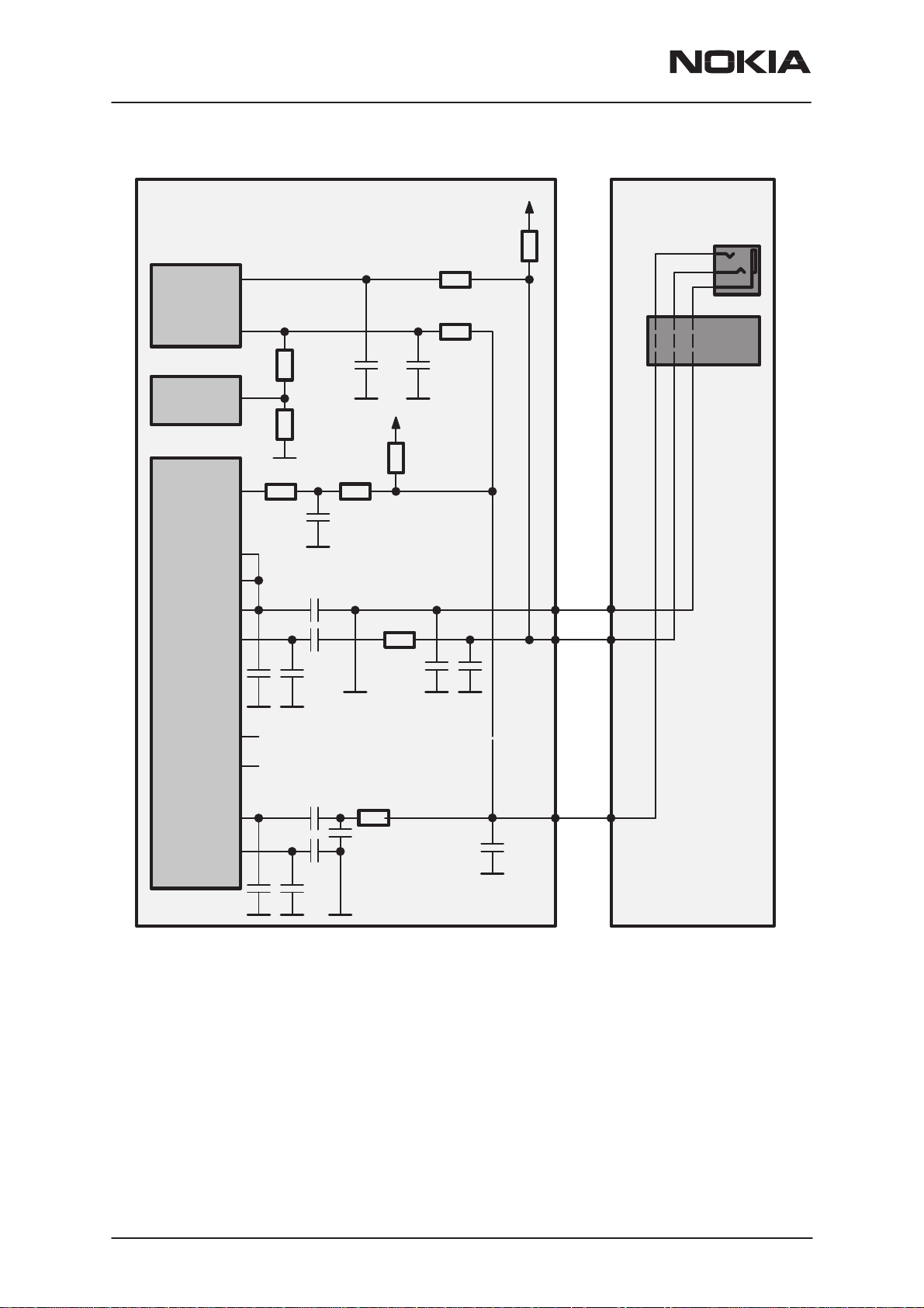
Power Distribution Diagram
The RF powering is described in the following picture. The baseband
powering concept is included in the baseband block diagram.
Issue 1 12/99
Nokia Mobile Phones Ltd.
Page 9
Page 10
Page 10
F
4.75 V ... 5.25 V FET switch
PCMCIA slot
RPM-1
System Module
VPAVcc
4*680uF+3*470uF tantalum capacitors
Nokia Mobile Phones Ltd.
CCONT
2 mA
VCTCXO
+Buffer
Issue 1 12/99
VXO
VR
1
VR
2
40 mA
SUMMA RX
VRX_2
VR
3
10 mA
Synthesizer
SUMMA:
VP1, VP2, VDD
VSYN_2
Pow.det.
VCOs
CRFU3:
Prescaler
UHF buffers
VR
4
40 mA
VSYN_1
VR
5
30 mA
CRFU3 &
SUMMA
RX
VRX_1
VR
6
12 mA
COBBA
ANAL.
VCOBBA
PAs
DCS: 1 A @ class 1 (50 Ohm Load)
GSM: 1.8 A @ class 4 (50 Ohm Load)
VR
VREF
7
< 10 uA
SUMMA
VREF
140mA
SUMMA & CHARGE
power detector OF PLL–IC
VTX
TXP
VXOENA
SYNPWR
RXPWR
TXPWR
V5V
PAMS Technical Documentation
0.2 mA (PLL locked)
PUMPsCRFU3 TX
VCP
Page 11
PAMS Technical Documentation
Connector Name Code
PCMCIA connector 5469079
SIM connector 5409063
Headset connector 5400083
Extension box subassembly (includes antenna insert and headset connector) 9477002
System Module
PCMCIA Interface
Supply voltages and all digital activity to external hosts go through the
PCMCIA interface. This interface is handled by SULO asic. In SULO asic
the PCMCIA interface section Vccs is PCMCIA connector Vcc. It is inde-
pendent from SULO core Vcc which is regulated to 2.8V from PCMCIA
connector Vcc.
The interface has two operating modes: one for PCMCIA compliant com-
puter hosts and one for non–PCMCIA (or vertical or Nokia mode) hosts.
The PCMCIA interface has two different pinouts. First is the normal
PCMCIA pinout which conforms to the PC Card’97 standard . Second
mode is the non–PCMCIA mode in which MBUS, FBUS and PCM SIO
buses are brought to the PCMCIA connector. Also flow control signals
and RESET are routed to the connector. The PCMCIA connector pinouts
and electrical characteristics are shown in the tables on the following
pages.
RPM-1
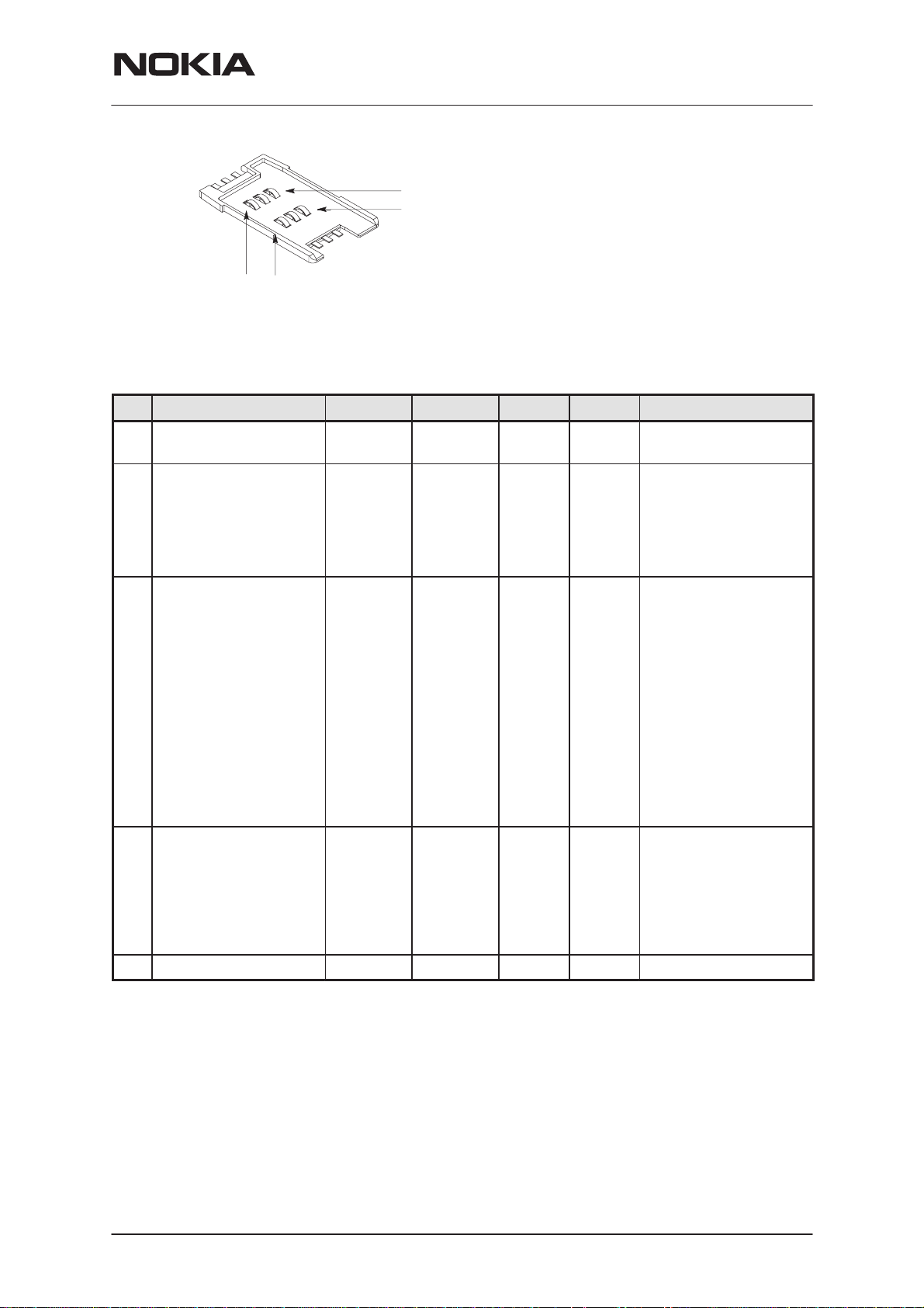
PCMCIA Connector
The 68–pin PCMCIA connector complies with the PC Card Standard
NO TAG which specifies the pinout and the functionality and electrical
characteristics of the pins. In the non–PCMCIA mode the functionality of
the pins is changed (see the following table).
No. 34
No. 68
No. 1
Issue 1 12/99
No. 35
Nokia Mobile Phones Ltd.
Page 11
Page 12
RPM-1
System Module
PAMS Technical Documentation
The pins of the PCMCIA connector are listed below:
PCMCIA mode Non–PCMCIA mode
Pin
Signal
name
1 GND Ground. Ground
2 D3 I/O Data bit 3. DSP Sleepnote OUT
3 D4 /IO Data bit 4. RIX OUT
4 D5 I/O Data bit 5. DCDX OUT
5 D6 I/O Data bit 6. CTSX OUT
6 D7 I/O Data bit 7. PCMTxDATA OUT
7 CE1X IN Card enable 1, pulled up Pulled up
8 A10 IN nc nc
9 OEX IN Output enable, pulled up pulled up.
Dir Function
Signal
name
Function Dir
10 A11 IN nc nc
11 A9 IN nc nc
12 A8 IN Address bit 8 Not used OUT
13 A13 IN nc nc
14 A14 IN nc nc
15 WEX IN Write enable, pulled up Pulled up.
READY/
16
IREQ
17 VCC Card power. Card power.
18 VPP1 nc nc
19 A16 IN nc nc
20 A15 IN nc nc
21 A12 IN nc nc
22 A7 IN Address bit 7 FBUSTxD OUT
23 A6 IN Address bit 6 FBUSRxD IN
24 A5 IN Address bit 5 DTRX IN
25 A4 IN Address bit 4 RTSX IN
26 A3 IN Address bit 3 PCM frame sync clk IN
OUT
Ready/busy, interrupt request.
Fixed 0. OUT
27 A2 IN Address bit 2 PCM data transmit clk IN
28 A1 IN Address bit 1 PCMRxDAT A IN
29 A0 IN Address bit 0
30 D0 I/O Data bit 0.
31 D1 I/O Data bit 1 DSRX OUT
32 D2 I/O Data bit 2. MCUSleepNote OUT
WP/
33
IOIS16X
Page 12
OUT
Write protect, I/O port is 16
bits wide, connected to VCC
Nokia Mobile Phones Ltd.
MBUS (Max. 2.8V),
Pulled up.
Connected to VCC
Issue 1 12/99
IN/
OUT
Page 13
PAMS Technical Documentation
Non–PCMCIA modePCMCIA mode
Pin
Pin
34 GND Ground. Ground.
35 GND Ground. Ground.
Signal
name
FunctionDir
Signal
name
RPM-1
System Module
DirFunction
36 CD1X OUT
37 D11 I/O nc nc
38 D12 I/O nc nc
39 D13 I/O nc nc
40 D14 I/O nc nc
41 D15 I/O nc nc
42 CE2X IN Card enable 2, pulled up Pulled up
43 VS1X OUT nc nc
RFU/
44
IORDX
RFU/
45
IOWRX
46 A17 IN nc nc
47 A18 IN nc nc
48 A19 IN nc nc
49 A20 IN nc nc
50 A21 IN nc nc
Card detect 1, connected to
Ground
IN I/O read strobe, pulled up Pulled up
IN I/O write strobe, pulled up Pulled up
Connected to Ground
51 VCC Card power. Card power.
52 VPP2 nc nc
53 A22 IN nc nc
54 A23 IN nc nc
55 A24 IN nc nc
56 A25 IN nc nc
57 VS2X OUT nc nc
58 RESET IN Card RESET, pulled up Card RESET, pulled up IN
59 WAITX OUT nc nc
RFU/IN-
60
PACKX
61 REGX IN
BVD2/SP
62
KRX
BVD1/STS
63
CHGX
64 D8 I/O nc nc
OUT Input port acknowledge. Fixed ’0’ OUT
Register and I/O select enable, pulled up
OUT Pulled up.
OUT
Status changed indication to
host device
Pulled up. IN
Select non–PCMCIA mode by
connecting to ground.
(pulled up)
Fixed ’1’ OUT
IN
Issue 1 12/99
Nokia Mobile Phones Ltd.
Page 13
Page 14
RPM-1
System Module
Pin
Pin
65 D9 I/O nc nc
66 D10 I/O nc nc
67 CD2X OUT Connected to ground. Connected to ground.
68 GND Ground Ground.
Signal
name
FunctionDir
PAMS Technical Documentation
Non–PCMCIA modePCMCIA mode
Signal
name
PCMCIA connector electrical specifications:
DirFunction
Pin Line
Symbol
PCMCIA-
signals
PCMCIA
signals
29 A0 Bidirectional MBUS 0V
Parameter Minimum Typical /
PCMCIA input signals, 0.0V
PCMCIA output signals 0.0V
SIM Interface
System asic MAD2WD1 controls the SIM card. All signals go through the
CCONT asic, where the level shifting of logical signals between
MAD2WD1 and SIM card are done . The CCONT contains also switched
mode supply for SIM–interface, called VSIM. MAD2WD1 controls the
VSIM voltage level (3V/5V) through control bus VSIM level is SIM car dependent..
To protect the SIM card from damage (when card is removed from
PCMCIA slot in power on state) there is a control signal, SIMCardDetx in
MAD2WD1.
2.4V
2.8V
2.1V
Nominal
LOW
HIGH
LOW
HIGH
LOW
HIGH
Maximum Notes
0.8V
VCC
+0.25V
0.5V
VCC
0.6V
2.8V
TTL or CMOS logic levels,
VCC=5V
TTL or CMOS logic levels,
VCC=5V
NOTE 2.8V is maximum in-
put voltage level. (This ap-
plies to NON–PCMCIA
only)
Active signal in that pin starts automatically the power down sequence.
The information from the removing is taken from PCMCIA RESET signal.
As power supply pins are longer, PCMCIA RESET pin is disconnected before power supply pins and internal pull up resistor activates the PCMCIA
RESET signal which activates the MAD2WD1 reset signal, MADPURX.
The MADPURX is delayed so, that there is enough time to drive SIM card
down before MAD goes to reset state.
All SIM reader signals withstand short circuit to ground without damage.
SIM Connector
SIM connector provides 6 contact pads for the SIM card according to the
GSM 11.11 standard.
Page 14
Nokia Mobile Phones Ltd.
Issue 1 12/99
Page 15
PAMS Technical Documentation
1
6
34
System Module
The pins of the SIM connector are listed below:
Pin Line Symbol Min Typ. Max. Unit Notes
RPM-1
1 SIMCLK Frequency
Trise/Tfall
2 SIMRST
5V SIM Card
3V SIM Card
Trise/Tfall
6 SIMDATA
5V SIM Card, logical
”1”
logical
”0”
3V SIM Card, logical
”1”
logical
”0”
Trise/Tfall
3,5 VSIM
5V level
Operating voltage, 3V
level
Output current
4.0
2.8
4.0
0.0
2.8
0.0
4.8
2.8
3.25
25
HIGH VSIM
100
HIGH
LOW
HIGH
LOW
5.0
3.0
VSIM
0.5
VSIM
0.5
1
5.2
3.2
MHz
ns
V
V
ns
V
V
V
V
us
V
V
SIM clock
SIM reset
SIM data
Supply voltage
Fullfill the GSM11.10
current spike requ.
30
4 GND Signal ground
Issue 1 12/99
Nokia Mobile Phones Ltd.
mA
Page 15
Page 16
RPM-1
Explanation
Explanation
System Module
PAMS Technical Documentation
The signals of the SIM interface are listed below:
SIM card CCONT
Pin name Direction Pin name Direction
VSIM VSIM SIM card operating voltage.
GND GND
SIMRST IN SIMRST_O OUT SIM RESET.
SIMCLK IN SIMCLK_O OUT SIM clock.
SIMDATA I/O DA TA_O I/O SIM data.
CCONT MAD2WD1
Pin name Direction Pin name Direction
SIMRST_A IN SIMCardRstX OUT SIM RESET from MAD2WD1
SIMCLK_A IN SIMCardClk OUT SIM clock from MAD2WD1
DATA_A I/O SIMCardData I/O SIM data to/from MAD2WD1
SIM I/O_C IN SIMCardIOC OUT
SIM_PWR IN SIMCardPwr OUT SIM power control (on/off)
SIM ground. Connected to common
ground of the phone.
SIM data direction control from
MAD2WD1. When LOW, data flow from
MAD2WD1 to CCONT.
SIM connector electrical specifications:
Conn./Pin. Name/Line Symbol Min T yp. Max. Unit Comments
X700/1
SIMCLK
X700/2
SIMRST
X700/6
SIMDATA
X700/5
VSIM
SIMCLK Frequency
Trise/Tfall
5V SIM Card
3V SIM Card
Trise/Tfall
5V SIM Card, logical ”1”
logical ”0”
3V SIM Card, logical ”1”
logical ”0”
Trise/Tfall
Operating voltage, 5V level
Operating voltage, 3V level
Output current
4.0
2.8
4.0
0.0
2.8
0.0
4.8
2.8
3.25
25
HIGH VSIM
100
HIGH
LOW
HIGH
LOW
5.0
3.0
VSIM
0.5
VSIM
0.5
1
5.2
3.2
30
MHz
ns
V
V
ns
V
V
V
V
us
V
V
mA
SIM clock
SIM reset
SIM data
Supply voltage
Fullfill the
GSM11.10 cur-
rent spike requ.
Page 16
Note that the SIM card reader (X700) pin numbers are NOT the same as
pin numbers of the SIM card.
Nokia Mobile Phones Ltd.
Issue 1 12/99
Page 17
PAMS Technical Documentation
Im edance
50ohm
tor
Antenna or RF Connector
Antenna or RF connector contacts are listed below:
RPM-1
System Module
Con-
tact
1 EXT_ANT
2 GND
Line
Symbol
Parameter Mini-
mum
p
Loss in GSM
band
Loss in PCN
band
Headset or Analog Audio Interface
The Headset or Analog audio signals to the headset connector are coming from COBBA_GJP audio codec. Audio signals from COBBA_GJP to
headset connector goes through RF block in the PCB layout, and connector is near the antenna. Because of that there must be EMI protection circuit near the headset connector and also in COBBA_GJP side.
Typical
/ Nomi-
nal
Maxi-
mum
External antenna connec0 V DC
0.6 dB
1.0 dB
Unit / Notes
,
Issue 1 12/99
Nokia Mobile Phones Ltd.
Page 17
Page 18
RPM-1
System Module
PAMS Technical Documentation
Baseband
HookDet
MAD
HeadDet
CCON
T
AUXOUT
EA
D
EAR
N
EAR
P
HFC
M
VCOBBA
RF
Headset
connector
MIC
EAR
COM
EMI protection
(low impedance
in audio freq.)
VCOBBA
SGN
D
H
F
XEAR
HSGND
HSEAR
COBBA_GJP
MIC1
N
MIC1
P
MIC3
N
MIC3
P
Headset Connector
XMI
C
HSMIC
Page 18
The headset connector is used to connect the HDC–6D headset to
RPM–1. HDC–6D has a 2.5 mm stereo plug connector.
Nokia Mobile Phones Ltd.
Issue 1 12/99
Page 19
PAMS Technical Documentation
HookD
ead e s g a
HeadDet signal
1
3
24
Electrical specifications for the Headset interface
Pin Name Function Min Typ Max Unit Description
3 HSEAR Analog audio output
Accessory detection with
et signal.
2 HSMIC Headset microphone input
Headset detection with
HeadDet signal.
Micbias on
22 Output AC impedance (ref. GND)
10 F Series output capacitance
16 150 300 Load AC impedance to GND: Headset
1.0 V
0.56 V DC Voltage (level in MAD–ASIC, ”0”<0.2*VBB).
0 0.2 V DC Voltage (ref. HSGND). Headset with closed
16 250 1500 Load DC resistance to HSGND. Headset with closed
1.96 V DC Voltage (ref. HSGND). Headset with open switch
47 k Pull–up resistor to VBB in RPM–1
2.0 2.2 k Input AC impedance (Micbias on)
2.5 k Headset source impedance
100 300 500 A Bias current (Note! Micbias 2.1 V)
200 mV
47 k Pull–up resistor to VBB in phone
1.2 1.7 V Headset connected.
2.1 V Headset not connected.
Max. output level. No load
p–p
switch
switch
Maximum signal level
p–p
RPM-1
System Module
Headset detection with
Micbias off
Micbias 2.1 V Switched on when call is on and headset is in.
1 HSGND Audio signal ground
(=AGND).
4 GND Ground 0 Ground
Issue 1 12/99
.
Nokia Mobile Phones Ltd.
0 0.1 V Headset connected.
2.5 2.9 V Headset not connected.
0 Is the same than GND in the phone, they have been
connected together by a 0 ohm resistor.
Page 19
Page 20
RPM-1
System Module
Modes of Operation
Standard PCMCIA mode
This is the standard operating mode of the RPM–1. The card is used as a
standard 8–bit PCMCIA I/O device. In this mode the card can be used in
two different sub–modes: Nokia–mode and generic mode. In generic
mode the card functions just as a normal modem card and no RPM–1–
specific SW drivers are needed in the PC. In Nokia–mode an improved
power management is offered (deep sleep), but this requires the use of
RPM–1–specific SW drivers in the PC.
The host PC automatically configures its internal memory and interrupt
mapping based on so called CIS data structure (Configuration Information
Structure, specified by the PC card standard) which is stored in the serial
EEPROM in the card and loaded into Sulo ASIC at startup. The PCMCIA
ASIC (Sulo) also contains the following standard PC card registers: Configuration Option Register (COR), Configuration and Status Register
(CSR), and Extended Status Register (ESR). See document NO TAG for
details.
PAMS Technical Documentation
PCMCIA connector signals are listed in NO TAG.
Vertical (i.e. non–PCMCIA) mode
For host devices not having a PCMCIA slot the RPM–1 has been designed to support also simple direct serial bus operation. In this mode the
PCMCIA connector signals have been redefined to support new logical
interfaces. PCMCIA connector signals in non–PCMCIA mode are listed in
NO TAG.
Typical RPM–1 host interface is RS232C. The application specific socket
for the RPM–1 is assumed to contain all 5V to RS232C buffering circuitry.
The vertical operating mode is activated by grounding pin 62
(SPKR#/BVD2) in the PCMCIA connector before card RESET is released.
Pin 62 (SPKR#/BVD2) must be kept grounded all the time when operating
in non–PCMCIA mode. The SPKR#/BVD2 pin has an internal pull–up resistor ensuring standard PCMCIA mode operation if the pin is left unconnected.
Maximum Ratings
Sym-
bol
Vcc Supply voltage –0.5 to 5.5 V
Parameter Ratings Unit Comments
VI Input voltage range –0.5 to Vcc+0.5 V
Vo Output voltage range –0.5 to Vcc+0.5 V
Page 20
Nokia Mobile Phones Ltd.
Issue 1 12/99
Page 21
PAMS Technical Documentation
bol
IIK Input clamp current
±20
RPM-1
System Module
CommentsUnitRatingsParameterSym-
mA
IOK Output clamp current
Max. operating temperature
range
±20
–10 to +55 _C
mA
DC Characteristics
Supply voltages and Power consumption
Conn./Pin. Name/Line Symbol Min T yp. Max. Unit Comments
PCMCIA/
17,51
PCMCIA/
17,51
PCMCIA/
17,51
PCMCIA/
17,51
PCMCIA connector supply
voltage Vcc
PCMCIA supply current (Vcc)
during CIS reading
PCMCIA supply current
(Vcc=5.0V)
in IDLE state
PCMCIA supply current
(Vcc=5.0V) in CALL state
(2+2, 0.8W)
4.75 5.0 5.25 V Operating voltage range
32 40 mA Absolute max.
supply current
during CIS read-
ing is 70mA.
30 40 mA 1A is absolute
max. current
from PCMCIA
connector.
480 mA Average current
when using
max. transmit
power (GSM)
and multislot
transmission
Issue 1 12/99
E Nokia Mobile Phones Ltd.
Page 21
Page 22
Page 22
RPM-1
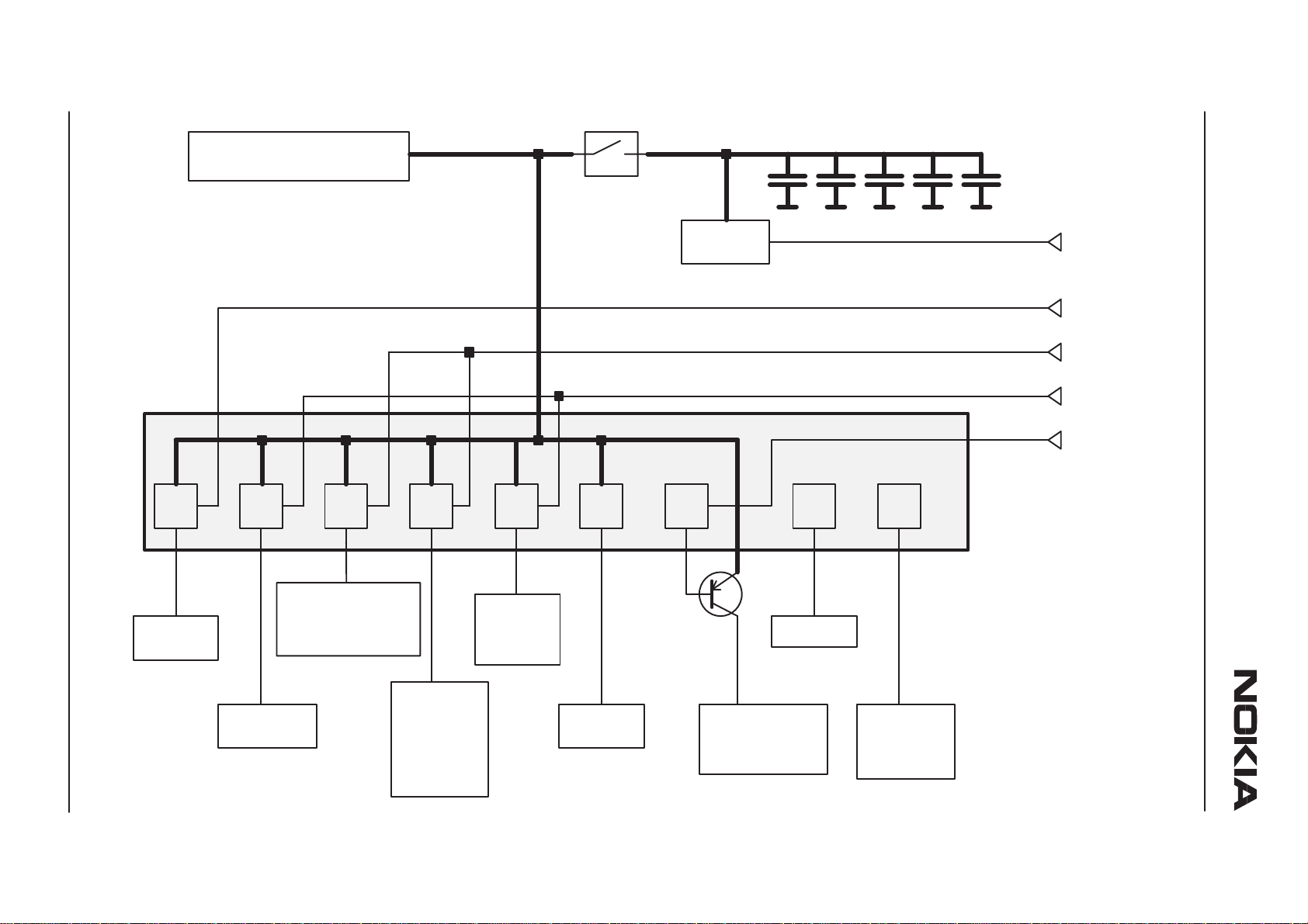
Introduction to baseband
System Module
Vcc 4.75...5.25 Vdc
Nokia Mobile Phones Ltd.
PCMCIA bus
Vcc
Lin. Reg.
2.8 Vdc
N400
PCMCIA Connector X400
Vcc
10k
BVD2/SPKR#
Vsulo
CIS
EEPROM
(Serial)
D401
Issue 1 12/99
A0
256*8
SIM
reader
X700
NTC
N701
SULO
PCMCIA
interface
ASIC
D400
V5V_2
SIM
Vref
100k
BTEMP
CCONT
Regulator
ASIC
VBAT
N700
PURx
MADPURx
Trace Bus
FBUS
PCM
Flow control
MCUSleepNote
DSPSleepNote
WakeUpInt
COBBA AudioSel
ModeStatus
FLASH Clk
MBUS SW
D402
COBBA PCM
13MHz
VBB
SleepCLK
SIMif
CNTVR
MBUS
VBB
VPA
V5V VCP
VR1
VR2
VR3
VR4
VR5
VR7
VXO
VRX_2
VSYN_2
VSYN_1
VRX_1
VTX
VR6
Vref
V2V
2.425 V
Core
MAD2WD1
VBB
IOs
VBB
COBBA_GJP
COBBA bus TX/RX signals
13MHz
RFI+
CODEC
N600 X601
Vref
Headset
HeadDet, HookDet
MCU
System logic
DSP
SRAM, ROM
Sdata/Sclk/Sena1/Sena2
13MHz
PDATA0
Band Sel
TXP
RFC
D500
VPPEN
Memory bus
VBB
FLASH SRAM
VPP SW
V703
VPP
D501 D502
128k*161M*16
RF
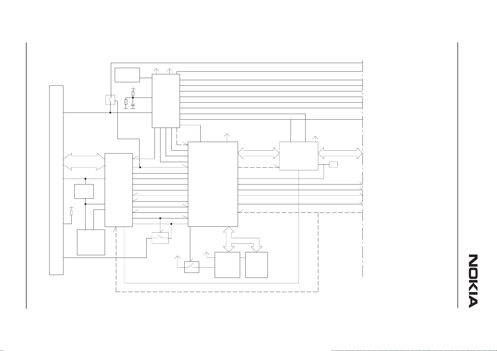
This section of the document specifies the BB section of the GX9 RF/sys-
tem module for RPM–1.
The baseband block diagram is below:
PAMS Technical Documentation
Page 23

PAMS Technical Documentation
Functional Description
Power Distribution
The supply voltage (VCC) from PCMCIA slot goes to the CCONT VBAT
pins, Sulo ASIC and Sulo core voltage regulator. Also transmit power amplifier (PA) is connected to VCC via FET switch and MBUS switch is powered from VCC rail.
The voltage to power amplifier is connected via delayed FET switch,
which is turned on slowly after the card is powered by host computer, and
CIS information has been read. The VPA line has capacitor array, and to
avoid the inrush current the FET switch is delayed so, that current spike is
under 300mA in the beginning.
Because the SULO ASIC must be powered all the time when the RPM–1
is in PCMCIA slot of the host computer, it needs own regulator for core
voltage. The SULO ASIC draws the core voltage supply from low dropout
regulator, which regulates PCMCIA voltage (Vcc) to 2.8V. The CIS EEPROM takes supply voltage from the same regulator. Secondary supply
voltage (Vcca) to SULO is taken directly from PCMCIA supply voltage
(Vcc). This voltage set the logic levels for PCMCIA interface (5V).
RPM-1
System Module
The CCONT includes all the voltage regulators and feeds the power to
the whole RF and BB system (except SULO, CIS EEPROM and TX power
amplifiers). The MAD2WD1 IOs, COBBA_GJP digital parts and memories
are powered from the same regulator which provides 2.8V baseband supply VBB. The baseband regulator is active always when the CCONT supply voltage is higher than 3.1 V. There is also a separate regulator for SIM
card. The VSIM regulator output is selectable between 3V and 5V, controlled by MAD via serial control bus. COBBA_GJP analog parts are powered from dedicated 2.8V supply, VCOBBA, by the CCONT. CCONT includes also voltage reference regulator for COBBA_GJP analog parts,
temperature measurement and RF block.
The CCONT has six additional 2.8V regulators providing power to the RF
section. These regulators can be controlled either by direct control signals
from MAD or by RF regulator control register in CCONT which MAD can
update.
The switched mode regulator, V5V, is used for SUMMA and Integral PLL
charge pump supply VCP. This voltage can be controlled on and off with
serial IO bus.
The CCONT programmable regulator, V2V, is used as a power source for
MAD2WD1 core. The V2V level in startup is set to 1.975V. The right voltage level for the MAD2WD1 C07 core is 1.75 V (1.65 ... 1.95 V). This level is set by MCU SW before DSP release and normal operation. Detailed
information about V2V setting can be found in ”CCONT V2V User’s
Manual” NO TAG.
The VPP voltage is used for FLASH memory programming, when MCU
code is downloaded to the FLASH memory and when EEPROM emula-
Issue 1 12/99
Nokia Mobile Phones Ltd.
Page 23
Page 24
RPM-1
System Module
tion blocks of FLASH memory are updated. The VPP voltage is taken
from VBB power net through a voltage switch. VPP is enabled with
MAD2WD1 general I/O pin, MCUGenIO4.
DC Characteristics of the CCONT voltage regulators are listed below:
PAMS Technical Documentation
Reg. on/off-
Control
line in
CCONT
VR1 SLEEPX Supply voltage
VR2 CNTVR2 Supply voltage
VR3 CNTVR3 Supply voltage
VR4 CNTVR4 Supply voltage
VR5 CNTVR5 Supply voltage
VR6 SLEEPX Supply voltage
VR7 TXPWR Supply voltage
VBB Supply voltage
VSIM SIMPWR Supply voltage
V5V Supply voltage
V2V Programmable,
VRef Supply voltage
Parameter Min. Typ. Max. Unit Comments
Supply current
Supply current
Supply current
Supply current
Supply current
Supply current
Supply current
Supply current (on)
(sleep)
Supply Voltage
Supply current
Supply current
Supply voltage
Supply current
Supply current
2.7 2.8 2.85
80
2.7 2.8 2.85
80
2.7 2.8 2.85
50
2.7 2.8 2.85
80
2.7 2.8 2.85
80
2.7 2.8 2.85
80
2.7 2.8 2.85
150VmA
2.7 2.8 2.85
125
1
2.8
4.8
4.8 5.0 5.2
1.3 2.65
1.478 1.5 1.523
3.0
5.0
3.2
5.2
330
30
50
200
V
VCTCXO voltage,
mA
mA
mA
mA
mAmACurrent limit 250mA
uA
mA
mA
controlled by MAD
(VCXOPwr)
VmARx part voltage, con-
trolled by MAD
(RxPwr)
V
V
VmARx part voltage, con-
V
V
V
V
V
V
VuAReference voltage to
VSYN_2 voltage,
controlled by MAD
(SynthPwr)
VSYN_1 voltage,
controlled by MAD
(SynthPwr)
trolled by MAD
(RxPwr)
VCOBBA voltage,
controlled by MAD
(VCXOPwr)
Tx voltage, con-
trolled by MAD
(TxPwr)
Current limit 5mA
Voltage (3V/5V) is
selected by MAD via
control bus
SUMMA/FPLL
charge pump volt-
age.
Initilal state 1.975V,
Is set to 1.75 V
after startup
COBBA_GJP and
SUMMA
Power up
The only way to power up RPM–1 is to insert it in to a 68 pin PCMCIA
connector. The connector may be either in a PCMCIA compliant slot, or a
Page 24
Nokia Mobile Phones Ltd.
Issue 1 12/99
Page 25
PAMS Technical Documentation
NOKIA proprietary non–PCMCIA slot. The host computer or controller
connects power to the card after it has detected the card in it’s slot.
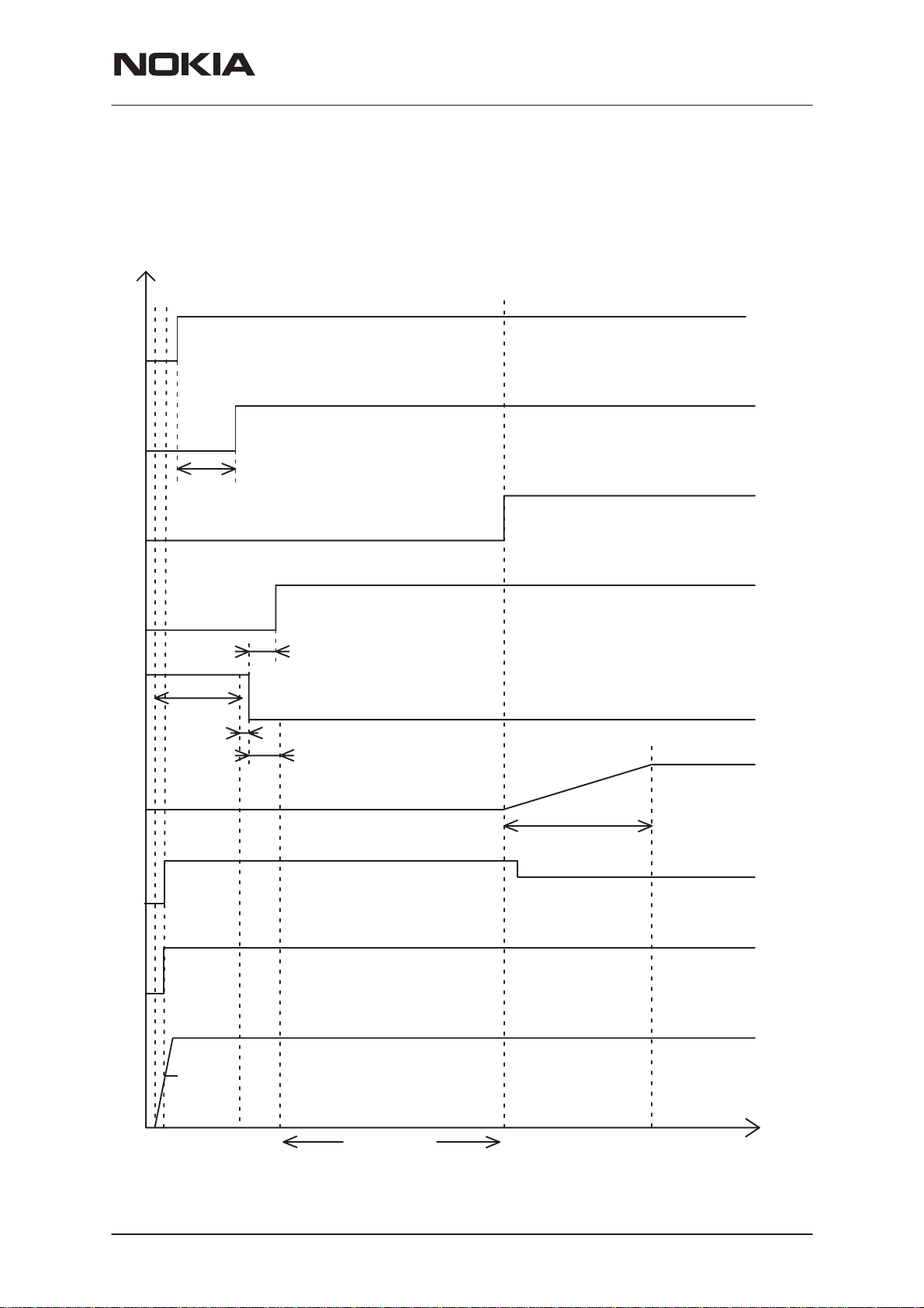
Power–Up in PCMCIA mode
RPM-1
System Module
VPA
1
SLEEPX
0
1
CCONTPURx
0
1
62ms
MADPURx
0
1
PCMCIA slot IREQx/READY
0
1
100ms
0
10us
CIS information from EEPROM to Sulo RAM
PCMCIA slot RESET
20ms
1.975V
1.75 V
2.8V
Vcc
0
Max. 500ms
V2V, MAD core voltage (C07)
Power aplifier voltage, VPA
0
Baseband voltage VBB
0
PCMCIA Vcc
3.0V
3
1
2
4
CIS READING
5
6
Power up in PCMCIA mode takes place in following steps:
Issue 1 12/99
Nokia Mobile Phones Ltd.
Page 25
Page 26

RPM-1
System Module
PAMS Technical Documentation
1 As the card is inserted into PCMCIA slot, the host computer
connects supply voltage to it. The supply voltage is 5V. RESET
signal on PCMCIA interface floats and the card pulls it up with
a pull–up resistor.
2 When the input voltage exceeds 3.0V (typ.) the VBB is turned
on. After about 50us the SLEEPX is released and VCXO is
turned on. After 62ms delay the CCONTPURX is released.
3 After at least 100ms the host controller activates the reset sig-
nal. It keeps the RESET active (high) at least 10us. It releases
the RESET signal and waits for 20ms. The SULO keep the
IREQx/READY signal in busy state (low) during the CIS automatic loading from serial EEPROM into the SULO internal
RAM
4 Then the host computer first accesses the card and reads CIS
information from the internal RAM of SULO (The CIS information is automatically loaded from serial EEPROM into SULO
asic internal RAM after power up).
5 After reading CIS host computer checks the CIS information. In
its CIS information RPM–1 tells the computer that it is an I/O
card, so the computer switches it to I/O mode. The host computer reads the initial value of COR from CIS, writes it to COR
after CIS reading and releases MADPURX.
The host computer gives control of the RPM–1 to card drivers.
The drivers take care of further handling of the RPM–1.
After MADPURX release the MCU starts, read the core voltage, set it to the correct level and wakes up DSP. After the wakeup, MCU activates the DSRX bit. RPM–1 is then ready to accept AT–commands from the host computer.
6 When the MADPURX is released the PA–voltage FET switch is
turned on slowly to avoid current spikes. It’s take max 500ms
to turn FET switch totally open.
Power–Up in non–PCMCIA mode
Power–up in non–PCMCIA mode is simpler than power–up in PCMCIA
mode because the host controller does not access any registers or CIS in
the interface.
Page 26
Nokia Mobile Phones Ltd.
Issue 1 12/99
Page 27

PAMS Technical Documentation
RPM-1
System Module
VPA
1
SLEEPX
0
50us
1
CCONTPURx
0
62ms
1
MADPURx
0
1
PCMCIA slot IREQx/READY
0
1
PCMCIA slot RESET
0
Power aplifier voltage, VPA
1.975V
1.75 V
2.8V
Vcc
0
Max. 500ms
V2V, MAD core voltage (C07)
0
Baseband voltage VBB
0
PCMCIA Vcc
3.0V
1
2
3
4
time
Issue 1 12/99
Nokia Mobile Phones Ltd.
Page 27
Page 28

RPM-1
System Module
Following is the procedure to power–up the system in non–PCMCIA
mode.
PAMS Technical Documentation
1 First the supply voltage is applied to the card.
2 When the input voltage exceeds 3.0V (typ.) the VBB is turned
on. After about 50us the SLEEPX is released and VCXO is
turned on. After 62ms delay the CCONTPURX is released
which directly releases PURX to MAD2WD1 if PCMCIA RESET
signal is inactive (low).
3 After MADPURX release the MCU starts, identifies the MAD
chip version, configures CCONT to supply correct V2V core
voltage for present MAD chip (V2V during boot is 1.975 V and
correct core voltage for MAD2WD1 V9 C07 is 1.75 V) and
wakes up DSP. After the wakeup, MCU activates the DSRX
signal to Sulo. RPM–1 is then ready to accept AT commands
from the host computer.
4 When the MADPURX is released the PA–voltage FET switch is
Note: Holding PCMCIA RESET signal active MADPURx is also active
and PA voltage switch is closed. As MAD is held in reset state it can’t configure V2V to correct level. Boot up sequence is continued after host releases PCMCIA RESET.
Power down
There are three ways to power down RPM–1, power down with software,
brutal removal of supply voltage (equivalent to battery removal of regular
phone) and one is that supply voltage drops below the lower input voltage
limit.
When power down with software, first possible ongoing calls must be terminated and SIM card must be prepared for power down. Then the software of the host controller puts the RPM–1 in reset and cuts off its power.
When the supply voltage drop below 4.5 V the MAD2WD1 close down the
network and SIM card is prepared for power down. Then the CCONTPURX is activated and after that the CCONT is turned off. SULO outputs
to MAD2WD1 and COBBA_GJP are gated low (MAD2WD1 reads the
supply voltage level from CCONT ADC register).
turned on slowly to avoid current spikes. It’s take max 500ms
to turn FET switch totally open.
Page 28
When the user takes RPM–1 out of the PCMCIA slot (brutal power down)
the PCMCIA slot RESET signal goes high state before the voltage is cut
off (power supply pins are slightly longer). The PCMCIA RESET signal
activates MADPURX signal which activate SIMCardDetX and initializes
SIM power down sequence. The reset signal to MAD is delayed so, that
there is enough time to do SIM power–down sequence.
In non–PCMCIA mode the host controller must take care of power handling. The host controller must make sure that RPM–1 has no activities
Nokia Mobile Phones Ltd.
Issue 1 12/99
Page 29

PAMS Technical Documentation
going on when powering it down. Best procedure is to first activate the
external RESET and after a short delay cut off the power.
Card Temperature Measurement
Internal temperature of the cellular card phone is measured with CCONT
AD–converter. The temperature is converted to the voltage by using
NTC–resistor.
When the temperature inside the card increase higher than 85°C (highest
working temperature of industrial specified components), the user is informed by software, the ongoing activities are shut down and card power
is cut off.
Before cutting the power, software warns about the high temperature inside the card. The limit for that will be few degree lower.
The temperature sensor is 47 kΩ ±5 % NTC–resistor with B=4050 ±3 %.
Without any alignment, with NTC resistor and 1 % pull–up resistor ±5°C
accuracy is achieved in level of cut off temperature.
RPM-1
System Module
Audio Control
The audio control and processing in RPM–1 is taken care by COBBA_GJP, which contains the audio codec, and the MAD2WD1 which contains DSP block for handling and processing the audio signals.
Analog audio
The headset (type HDC–6D) can be connected to the system via headset
connector, located in the extended part, near the antenna.
The headset connection is made following way:
In HSMIC signal there is a pull–up resistor in the RPM–1. The micro-
phone of the headset is a low resistance pull down compared to that.
When there is no call in progress, AUXUOT (=Micbias output of the COB-
BA ASIC) is in high impedance state and HSMIC is pulled up. When
headset is connected, HSMIC is pulled down. HSMIC is connected to
HeadDet–signal, which is an input to the CCONT and MAD ASICs. There
is a voltage measurement active in CCONT side and via it the presence
of the headset is noticed.
Also MAD–input of the HeadDet–signal could be used, but so far this
function has been implemented by CCONT. There is filtering between
HSMIC and HeadDet to prevent audio signal giving unwanted interrupts.
During a call there is bias voltage (2.1 V) in the AUXOUT.
The headset connection information is given also to Sulo by setting COBBAAudioSel signal. When headset is connected Sulo ASIC routes PCM
SIO bus from MAD2WD1 to COBBA_GJP.
In HSEAR signal there is also a pull–up resistor in the RPM–1. A remote
control switch of headset functions as a pull down. When remote control
Issue 1 12/99
Nokia Mobile Phones Ltd.
Page 29
Page 30

RPM-1
System Module
switch of the headset is open, there is a capacitor in series with earphone, so HSEAR (and HookDet interrupt signal to MAD2WD1) are
pulled up. When the switch is closed HookDet is pulled down by the headset.. The Truth Table is below.
PAMS Technical Documentation
No headset H H
Button HeadSet (Switch open) H
Button HeadSet (Switch closed)
Digital Control
The baseband functions are controlled by MAD2WD1 ASIC, which consists of MCU, system logic and DSP. This ASIC is part of MAD family,
specially designed for HSCSD, GSM/DCS solutions. MAD2WD1 based on
MAD2PR1, 144 pin DCT3.5 version MAD. The package of the MAD2WD1
is uBGA144.
The MAD2WD1 operates from 13MHz system clock, which is generated
from the 13MHz VCTCXO frequency. The system clock can be stopped
for a system sleep mode by disabling the VCTCXO supply power from
CCONT regulator output. The CCONT provides a 32kHz sleep clock for
internal use and the MAD2WD1. This 32kHz clock is used for a sleep
mode timing.
Memories
HookDet
L
HeadDet
L
L
FLASH Memory
The MCU program code resides in external FLASH memory, which size is
16Mbits (1M*16). FLASH memorys dedicated parameter blocks are used
instead of separate EEPROM memory to store other non–volatile data,
such as for example serial number, IMEI, tuning parameters and short
messages.
Used low voltage type FLASH memory’s access time is 110 ns and it is
CSP packaged.
SRAM Memory
The work memory is a Static RAM, and it’s size is 2Mbits (128k*16).
SRAM is powered with baseband voltage, VBB. The memory contents is
lost when the VBB voltage is switched off. All recallable data should be
stored into FLASH memory parameter blocks when the card is powered
down. SRAM access time is 70 ns and it’s package is TSOP(II)–44.
Reset
The CCONT generates the power up reset signal, CCONTPURX. This
reset signal is released after a 62ms delay from CCONT power up. This
Page 30
Nokia Mobile Phones Ltd.
Issue 1 12/99
Page 31

PAMS Technical Documentation
signal is used for making possible power on self reset in non–PCMCIA
mode. When CCONTPURX is active, all SULO outputs to MAD2WD1 and
COBBA_GJP are gated low.
The hard reset (Rst) comes from PCMCIA socket. The PCMCIA RESET
signal is pulled high (active) with an resistor and therefore the card is always in reset state after it has been inserted into a socket and before the
host drives the RESET signal.
The soft reset (SRst) is done by writing ’1’ to PCMCIA Configuration Option Register (COR) bit seven.
The MAD2WD1 reset signal (MADPURX) is active when any of following
resets is active : PCMCIA RESET, CCONTPURX or COR register bit 7 is
high.
Clocking
The system ASIC MAD2WD1 receives a 13MHz small signal clipped sine
wave from VCTCXO from RF block as a base clock. The clipped sine
wave is sliced to square wave inside MAD2WD1. The 13MHz square
clock signal is fed to COBBA_GJP. MAD2WD1 generates internally 26
MHz clock for MCU core and 78 MHz clock for DSP core from 13 MHz
base clock.
RPM-1
System Module
The PCMCIA interface ASIC Sulo receives also a 13MHz sine wave from
VCTCXO. Sulo contains a similar clock slicer block as the MAD2WD1
ASIC.
SIM card clock rates are 1.083 MHz, 1.625 MHz and 3.25 MHz. Default
clock rate is 3.25 MHz. SIM clock is generated by MAD2WD1. The level
of SIM clock can be 3 V or 5 V. This depends on the used SIM card. The
SIM card voltage level is controlled by MAD2WD1 and the voltage conversion is done in CCONT.
The CCONT ASIC generates 32.768kHz sleep clock for MAD2WD1. This
32kHz clock is used in sleep mode to keep the system synchronized with
network. In sleep mode 13MHz clock is turned off.
Sleep Mode
Sleep mode is used in idle time when there is no call going on. Between
paging blocks the system just waits for next paging block and may as well
go into sleep. The sleep mode is used for decreasing average idle current.
In RPM–1 the sleep mode can be set only in PCMCIA mode when Nokia
specific driver is used in host computer.
In the sleep mode all the regulators, except the baseband VBB, V2V and
the SIM card VSIM, regulators are off. Sleep mode is activated by the
MAD2WD1 after MCU and DSP clocks have been switched off. The voltage regulators for the RF section are switched off and the VCTCXO pow-
Issue 1 12/99
Nokia Mobile Phones Ltd.
Page 31
Page 32

RPM-1
System Module
er control, VCXOPwr is set low. In this state only the 32kHz sleep clock
oscillator in CCONT is running. The Sulo ASIC goes to sleep mode when
both DSPSleepNote and MCUSleepNote are in sleep state. The
DSPSleepNote will be set active 100ms before DSP sets ACCIf clock off.
The MCUSleepNote goes active before MCU powers down the VCTCXO.
The status of both sleepnotes is shown in a register of Sulo, where the
Nokia PC driver can check it. Before writes and reads the PC driver must
make sure that system is not sleeping NO TAG.
The wakeup from sleep mode can be done by MAD2WD1 (the expiration
of a sleep clock counter). When DSPSleepNote or MCUSleepNote are in
awake state, Sulo is waked up. The Sulo wake up does not need sleep
clock, because the VCXO is running before one of the sleep notes is set
to wake state.
The wakeup can be done also by PC. When PC founds out that DSP or
MCU is sleeping (from SULO registers) it toggles the wakeup bit (in WakeUp register). This register is asynchronous and does not require any
clocks. Sulo generates external interrupt by toggling the MAD2WD1
ROW0 signal (configured to GenDet inside MAD2WD1 flexpool) and wakeup interrupt to MCU is generated. After MCU is waked up, it sends MDI
message to DSP. The message wakes up DSP and AccIf. THe PC driver
will continue polling the sleepnote status bits and notice when system is
up and running.
PAMS Technical Documentation
Page 32
Nokia Mobile Phones Ltd.
Issue 1 12/99
Page 33

PAMS Technical Documentation
Introduction to RF Section
This section of the document specifies the RF section of the GX9 RF/system module for RPM–1.
Block Diagrams
The RF block diagram :
RPM-1
System Module
Issue 1 12/99
Nokia Mobile Phones Ltd.
Page 33
Page 34

RPM-1
System Module
RF frequency plan
PAMS Technical Documentation
935–960
MHz
1805–1880
MHz
1710–1785
MHz
890–915
MHz
CRFU_3
193MHz
120 MHz
f/2
f
73 MHz IF
1950
–2073
MHz
UHF
PLL
TX IF 240 MHz
TX IF 120 MHz
f/2
f
f/2
f/2
SUMMA
60 MHz
f
f
2nd IF 13 MHz
f
f/2f/2
f
480
MHz
VHF
PLL
13 MHz
VCTCXO
RF characteristics
GSM part
The main RF characteristics of the GSM section are listed below:
Item Values
Receive frequency range 935 ... 960 MHz
Transmit frequency range 890 ... 915 MHz
Duplex spacing 45 MHz
Channel spacing 200 kHz
Number of RF channels 124
Power class 4 (with 1 Tx slot in PCMCIA mode *
and 2 Tx slots in Vertical mode *)
5 (with 2 Tx slots in PCMCIA mode*)
Number of power levels 15 (class 4) / 13 (class 5)
Page 34
Nokia Mobile Phones Ltd.
Issue 1 12/99
Page 35

PAMS Technical Documentation
System Module
GSM transmitter characteristics
Item Values
Type Upconversion, nonlinear, FDMA/TDMA
Intermediate frequency ( phase modulated ) 120 MHz (GSM) / 240 MHz (PCN)
LO frequency range 1010 ... 1035 MHz (UHFVCO = 2020 ... 2070
MHz)
Output peak power 2 W (33 dBm) @ class 4
0.8 W (29 dBm) @ class 5
Gain control range min. 30 dB
Maximum phase error ( RMS/peak ) max 5 deg./20 deg. peak
Maximum number of time slots / frame 2
Maximum power step between 2 Tx slots 28 dB
GSM receiver characteristics
RPM-1
Item Values
Type Linear, FDMA/TDMA
IF frequencies 1st 73 MHz, 2nd 13 MHz
LO frequencies 1st LO 1010 ... 1035 MHz, 2nd LO 60 MHz
Typical 3 dB bandwidth +/– 100 kHz
Sensitivity min. – 102 dBm , S/N >8 dB
Maximum number of time slots / frame 3 Rx + 1 Mon.
Maximum receiver voltage gain ( from antenna
to RX ADC )
Maximum step between Rx slots 30 dB
Receiver output level ( RF level –95 dBm ) 50 mVpp ( typical balanced signal level of 13
Accurate AGC amplifier control range 57 dB
Typical AGC step in LNA 39 dB
Usable input dynamic range –102 ... –15 dBm
RSSI dynamic range –110 ... –48 dBm
AGC relative accuracy on channel ( accurate
range )
Compensated gain variation in receiving band +/– 1.0 dB
73 dB, typical
MHz
IF in RF BB interface = input level to
RX ADCs )
+/– 0.8 dB
DCS1800 part
The carrier frequencies (MHz) are defined by the following formulas:
Issue 1 12/99
Channel number 512n885
TX frequencies Fl(n) = 1710.2 + 0.2 * (n–512)
RX frequencies Fu(n) = Fl(n) + 95
Nokia Mobile Phones Ltd.
Page 35
Page 36

RPM-1
System Module
PAMS Technical Documentation
The main RF characteristics of the DCS1800 section are listed below:
Item Values
Receive frequency range 1805 ... 1880 MHz
Transmit frequency range 1710 ... 1785 MHz
Duplex spacing 95 MHz
Channel spacing 200 kHz
Number of RF channels 374
Power class 1 / 2 , user selectable
Number of power levels 16
DCS1800 Transmitter characteristics
Item Values
Transmit frequency range 1710 to 1785 MHz
Type Upconversion
Intermediate frequency ( GMSK modulated ) 240 MHz
LO frequency range 1950 to 2025 MHz
Power class 1 and 2
Maximum output power +30 dBm (1.0 W) @ class 1
+24dBm (0.25W) @ class 2
Maximum number of time slots / frame 2
Maximum power step between 2 Tx slots 30 dB
DCS1800 receiver characteristics
Item Values
Receive frequency range 1805 to 1880 MHz
Type Linear, 3 IF
IF frequencies 1st 193 MHz, 2nd 73 MHz, 3rd 13 MHz
LO frequencies 1st LO 1998 to 2073 MHz, 2nd LO 120 MHz,
3rd LO 60 MHz
Typical 3 dB bandwidth 100 kHz
Sensitivity min. – 102 dBm , S/N >8 dB
Maximum number of time slots / frame 3 Rx + 1 Mon
Maximum receiver voltage gain ( from antenna
to RX ADC )
Receiver output level ( RF level –95 dBm ) 50 mVpp ( typical balanced signal level of 13
Accurate AGC control range 57 dB
Typical AGC step in LNA 37 dB
Page 36
Nokia Mobile Phones Ltd.
73 dB, typical
MHz IF in RF BB interface = input level to
RX ADCs )
Issue 1 12/99
Page 37

PAMS Technical Documentation
Usable input dynamic range –100 ... –23 dBm
RSSI dynamic range –110 ... –48 dBm
RPM-1
System Module
ValuesItem
AGC relative accuracy on channel ( accurate
range )
Compensated gain variation in receiving band +/– 1.0 dB
Maximum step between Rx slots 30 dB
+/– 0.8 dB
Issue 1 12/99
Nokia Mobile Phones Ltd.
Page 37
Page 38

RPM-1
System Module
Functional descriptions
RF block diagram
RF block diagram has conventional dual conversion receiver for GSM and
triple conversion receiver for DCS1800. Both receivers use upper side LO
drive in the first RF mixer, after that lower side LO drive is used. Because
of this there is no need to change I/Q phasing in baseband when receiving band is changed between DCS and GSM. The two receiver chains
are combined in 73 MHZ IF so they use same rx–chain from that point
down to 13MHz A–D converter. In transmitter side there are two image
rejection upconversion mixers, one for GSM and one for DCS 1800, for
the final TX–frequency. Both use upper side LO drive.
Architecture contains five ICs. Most of the functions are horizontally and
vertically integrated. UHF functions except power amplifier and VCO are
integrated into CRFU3, which is a RF–IC using bipolar process
(Ft=25GHz) suitable for 2GHz LNA– and mixer–functions. CRFU3 also
includes divide–by–two prescaler for UHF–VCO. Using this divider it is
possible to use only one UHF–VCO running at 2GHz. UHF synthesizer is
an external PLL–IC which uses 2GHz LO signal for both systems. This IC
includes PLLs for both UHF and VHF synthesizers. SUMMA PLL blocks
are programmed to power_down mode.
PAMS Technical Documentation
The selection between GSM and DCS1800 operation modes in CRFU3 is
done with mode selection signal derived from MAD2WD1 IC in baseband.
This signal controls the biasing circuitries of the different RF blocks in
CRFU3 so that GSM blocks and DCS1800 blocks are not active at the
same time. This way there is no need for extra voltage regulators and the
same CCONT regulator–IC can be used as in singleband DCT3 products.
Most of the RF–functions are in SUMMA which is a BiCMOS–circuit.
SUMMA is an IF–circuit including IQ–modulator with two buffered outputs
(one for GSM Tx IF and one for DCS1800 Tx IF), RX AGC amplifier and
RX mixer for 13 MHz down conversion. It also includes two operational
amplifiers for TX power control loop. There is one common input for power detector voltage and one for TXC–control and two outputs for power
control of the PAs (one for GSM and the other for DCS1800). The selection between GSM and DCS1800 operation modes is done via serial bus
of SUMMA.
Transmitter block consist of two separate PAs, one for GSM and one for
DCS1800. Both PAs are Hitachi modules having 50 Ohm input and output. Modules contain three amplifier stages and interstage matching. Tx
gain controls are also integrated into these PA modules.
Frequency synthesizers
Page 38
In RPM–1 RF module, external dual PLL–IC (NSC LMX2331L) is used to
meet the strict settling time requirements of multislot mobile. Both UHF–
Nokia Mobile Phones Ltd.
Issue 1 12/99
Page 39

PAMS Technical Documentation
and VHF–VCO are locked with PLLs into stable reference frequency ,
which is a 13MHz VCTCXO–module (Voltage Controlled Temperature
Compensated crystal oscillator).Temperature effect is controlled by AFC
(automatic frequency control) voltage in order to maintain VCTCXO
locked into frequency of the base station. AFC signal is generated by
baseband and converted to analog by using an 11 bit DAC in COBBA–
ASIC.
UHF PLL is a channel synthesizer for both GSM and DCS and is running
at approximately 2GHz. GSM local is generated by dividing UHF VCO frequency by two while DCS local is UHF VCO frequency itself. PLL IC includes N divider (consisting of dualmodulus (64/65) prescaler followed by
programmable divider), reference divider (R), phase detector and charge
pump for the external loop filter. Output of the UHF VCO is fed to N–divider which produces 200kHz input to the phase detector. Phase detector
compares this signal to 200kHz reference signal, which is the VCTCXO
output divided by R (65). Output of the phase detector is connected to
charge pump having current output. Charge pump current pulses charge
or discharge the integrator capacitor of the loop filter depending on the
phase differences of incoming signal fronts. Loop filter smoothens the
pulses and generates the DC control voltage which sets the UHF–VCO
frequency. The loop filter defines the step response of the PLL (settling
time) and the stability of the loop. It also defines the rejection of the reference sideband spurious and the integrated phase noise (rms/peak phase
error of the synthesizer). Because the settling time requirement of the
UHF synthesizer is so strict the component tolerances of the loop filter
and all the gain elements of the PLL have to be small. For that reason
special attention was paid to charge pump current tolerance. WD1 has
specified +/– 15% tolerance for the current in all operating conditions
(temperature, voltage source, output voltage, process changes). NSC has
proposed a special ’stamp of’ procedure to guarantee that. LMX2331LTM
EILI931 is a Nokia ’stamp off’ version of the standard PLL chip
LMX2331L.
RPM-1
System Module
VHF PLL is also located inside external PLL–IC. There is N divider (including 16/17 dual modulus prescaler followed by programmable divider),
reference divider, phase detector and charge pump for the loop filter. VHF
local signal is generated by a VHF VCO running at 480MHz. VHF local is
common for both GSM and DCS1800. VHF–PLL is locked to the same
13MHz VCTCXO reference as UHF PLL .
Issue 1 12/99
Nokia Mobile Phones Ltd.
Page 39
Page 40

RPM-1
System Module
Synthesizer block diagram
R
PAMS Technical Documentation
freq.
reference
AFC–controlled VCTCXO
f
ref
f_out /
LO to DCS1800
N
PHASE
DET.
CHARGE
PUMP
Kd
LP Kvco
VCO
N
LO to GSM
Dividers and control registers of the synthesizer are controlled via serial
bus. SDATA is programming data, SCLK is serial clock and SENA1 is a
latch enable for SUMMA and SENA2 is latch enable of external PLL. The
PLL blocks in SUMMA are programmed to power–down mode. The power supply voltages of the SUMMA are connected to the ground to minimize the power consumption.
f_out
2
f_out/2
Receivers
There is a different frontend for both bands. The frontends are placed
from antenna to the 73 MHz IF. From 73 MHz IF to the baseband the RX
parts are common for both bands.
GSM frontend
GSM receiver is a dual conversion linear receiver. This frontend in
CRFU3 RF–ASIC is activated with BAND_SEL signal set to high–state.
Received RF–signal from the antenna is fed via the duplex filter to LNA
(low noise amplifier) in CRFU3. Active parts (RF–transistor and biasing
and AGC–step circuitry) are integrated into this chip. Input and output
matching networks are external. Gain selection is done with PDATA0 control. Gain step in LNA is activated when RF–level in antenna is –47 dBm.
After the LNA, amplified signal (with low noise level) is fed to bandpass
filter, which is a SAW–filter.
This bandpass filtered signal is then mixed down to 73 MHz, which is the
first GSM intermediate frequency. 1st mixer is located into CRFU3 ASIC.
Page 40
Nokia Mobile Phones Ltd.
Issue 1 12/99
Page 41

PAMS Technical Documentation
This integrated mixer is a double balanced Gilbert cell. All active parts
and biasing are integrated and matching components are external. Because this is an active mixer it also amplifies IF–frequency. Also local signal buffering is integrated. First local signal is generated with UHF–synthesizer by using upper side injection.
DCS1800 frontend
DCS receiver is a triple conversion linear receiver. This frontend in
CRFU3 is activated with BAND_SEL signal set to low–state. Received
RF–signal from the antenna is fed via the diplexer, Rx/Tx switch and frontend filter (Pre LNA filter) to LNA (low noise amplifier) in CRFU3. Active
parts (RF–transistor and biasing and AGC–step circuitry) are integrated
into this chip. Input and output matching networks are external. Gain
selection is done with PDATA0 control. Gain step in LNA is activated
when RF–level in antenna is –47 dBm. After the LNA amplified signal
(with low noise level) is fed to bandpass filters. RX frontend and RX interstage bandpass filters together defines, how good are the blocking characteristics against spurious signals outside receive band and the protection against spurious responses.
RPM-1
System Module
This bandpass filtered signal is then mixed down to 193 MHz IF, which is
first intermediate frequency of the PCN band. 1st mixer is in CRFU3
ASIC. This integrated mixer is a double balanced Gilbert cell. All active
parts and biasing are integrated, only matching components are external.
Because this is an active mixer it also amplifies IF–frequency. Also local
signal buffering is integrated and upper side injection is used. First local
signal is generated with UHF–synthesizer. There is a balanced LC–bandpass filter in the output of the first mixer which e.g. attenuates the critical
167MHz spurious and 156.5 MHz half–if frequency. It also matches impedance of 193MHz output to following stage input.
After this filter, the 193 MHz IF–signal is mixed down to 73 MHz IF, which
is second intermediate frequency of the PCN band (1’st IF of GSM). This
VHF–mixer is also double balanced Gilbert cell and is located into
CRFU3. Lower side LO signal is used. This 120MHz LO signal is got from
SUMMA–ASIC where it is derived by dividing 480MHz VHF LO signal by
four. There is an external lowpass filter for this 120MHz LO signal .
Common receiver parts for GSM and DCS 1800
After the GSM RX–mixer and DCS VHF–mixer, the RX–signal path is
common for both systems. This 73 MHz IF–signal is bandpass filtered
with a selective SAW–filter. From the mixers‘ outputs to IF–circuit input of
SUMMA–ASIC, signal path is balanced. IF–filter provides selectivity for
channels greater than +/–200 kHz. Also it attenuates image frequency of
the following mixer and intermodulating signals.
Next stage in the receiver chain is an AGC–amplifier. It is integrated into
SUMMA–ASIC. AGC gain control is analog. Control voltage for the AGC
is generated with DA–converter in COBBA–ASIC in baseband. AGC–
Issue 1 12/99
Nokia Mobile Phones Ltd.
Page 41
Page 42

RPM-1
System Module
stage provides accurate gain control range (min. 57 dB) for the receiver.
After the AGC–stage, the 73MHz IF–signal is mixed down to 13 MHz. The
needed 60 MHz LO signal is generated in SUMMA by dividing VHF–synthesizer output ( 480 MHz ) by eight.
The following IF–filter is a ceramic bandpass filter at 13 MHz. It attenuates adjacent channels, except for +/– 200 kHz there is not much attenuation. Those +/– 200 kHz interferers are filtered digitally by the baseband. Because of this RX ADCs have to be so good, that there is enough
dynamic range for the faded 200 kHz interferer. Also the whole RX has to
be able to handle signal levels in a linear way. After the 13 MHz filter
there is a buffer for the IF–signal, which also converts and amplifies
single ended signal from filter to balanced signal for the buffer and AD–
converters in COBBA. Buffer in SUMMA has voltage gain of 36 dB and
buffer gain setting in COBBA is 0 dB.
RX interstage filter
PAMS Technical Documentation
GSM RX filter is a bandpass SAW filter. It attenuates the out–of–band
blocking signals, image frequency and spurious responses derived from
blocking requirements. It has single ended input and balanced output.
The specification is in the next table.
Parameter Min. Typ. Max. Unit
Passband 935 – 960 MHz
Insertion loss 3.8 dB
Ripple in passband 1.0 dB
Attenuation DC...890 MHz 35 dB
Attenuation 890...915 MHz 15 dB
Attenuation 980...1030 MHz 15 dB
Attenuation 1070...1500 MHz 35 dB
Terminating impedance, input 50 ohm, single–ended
Terminating impedance, output 50 ohm, balanced
VSWR 2.0
Maximum drive level +10 dBm
GSM UHF–mixer in CRFU3
GSM UHF mixer is a double balanced Gillbert cell. The RF input and IF
output are differential type.
Parameter min. typ. max. unit notes
Input RF–frequency 935 960 MHz
Output IF–frequency 73 MHz
Input LO–frequency 1008 1033 MHz
Power gain
Rload = 2k
Page 42
7 8 9 dB GSM IF=73MHz,
Nokia Mobile Phones Ltd.
LO=1008 – 1033 MHz
overall gain variation
Issue 1 12/99
Page 43

PAMS Technical Documentation
RPM-1
System Module
notesunitmax.typ.min.Parameter
Relative gain variation
over temperature ran–
ge.
NF, SSB 10 12 dB
IIP3 tbd. +3 dBm
1 dB input compression
point
1/2 IF spurious re-
sponse.
Specified value is level
of interferer in mixer
input.
RF–IF isolation Not
+/–0.5 dB VRX=2.8V
–7 –5 dBm
–21 dBm Fwanted=935MHz
dB
Available
DCS1800 receiver frontend
F=942.5MHz
Pwanted=–85dBm
Finterferer=971.5MHz
These signals are fed
to mixer input. Level of
IF signal caused by interferer is adjusted to
be the same as wanted
IF signal level in mixer
output.
DCS receiver’s frontend consists of diplexer, Rx/Tx switch, Pre LNA filter,
LNA, UHF– and VHF–mixers which are in CRFU3–ASIC and RF–interstage– and 193MHz VHF– filters.
Pre LNA filter
Parameter Min. Typ. Max. Unit
Passband 1805–1880 MHz
Terminating impedance 50 ohm
VSWR 2
Insertion loss in passband 3 dB
Amplitude ripple in passband 1.5 dB dB
Attenuation DC–1630 MHz 25 dB
Attenuation 1630–1705 MHz 22 dB
Attenuation 1705–1790 MHz 10 dB
Attenuation 1898–1920 MHz 7 dB
Attenuation 1920–1980 MHz 10 dB
Attenuation 1980–2179 MHz 18 dB
Attenuation 2179–2254 MHz 40 dB
Attenuation 2254–3700 MHz 15 dB
Attenuation 3700–12000 MHz 10 dB
Maximum drive level +10 dBm
Issue 1 12/99
Nokia Mobile Phones Ltd.
Page 43
Page 44

RPM-1
System Module
PAMS Technical Documentation
The most important parameters are attenuation in 2179–2254 MHz and in
general the attenuation below 3.7 GHz.
DCS1800 LNA in CRFU3
Parameter min. typ . max. unit notes
Specified frequency 1805 1880 MHz
Gain 13.8 15 16 dB Overall gain variation
relative gain variation
over temperature range
relative gain variation
over frequency range
NF 1.6 2.0 dB
NF, when AGC=L Not
IIP3 –8 dBm
1 dB input compression
point
Absolute gain reduction 31 dB AGC=L
Relative step accuracy +/– 2 dB Over temp. range
LNA switching time 1 us
AGC settling time 1 us
AGC, SEL input H 1.9 V
AGC, SEL input L 0.8 V
AGC input current 1 uA AGC=H,L
LNA current consump-
tion
Reverse isolation 18 dB =S12 when matched.
–18 dBm AGC=H
+/–0.5 dB VDDRX=2.8V
f=1842.5MHz
+/–0.5 dB Tamb=25*C
VDDRX =2.8V
dB
Available
AGC=L
in room temperature
5 mA AGC=H
RX interstage filter
This is a SAW filter which attenuates the image and spuriouses derived
from blocking requirements. There should has balanced output or balun
between filter and RF input of the UHF mixer.
Parameter Min. Typ. Max. Unit / notes
Passband 1805 – 1880 MHz
Terminating impedance 50 ohm
Insertion loss in passband 3.5 dB
Amplitude ripple in passband 1.0 dB
VSWR in passband 2.0
Attenuation DC ... 1705 MHz 25 dB
Attenuation 1980 ... 2500 MHz 25 dB
Page 44
Nokia Mobile Phones Ltd.
Issue 1 12/99
Page 45

PAMS Technical Documentation
Attenuation 2500 ... 3700 MHz 20 dB
Attenuation 3700 ... 6000 MHz 15 dB
Maximum drive level +10 dBm
DCS1800 UHF mixer
DCS UHF mixer is a double balanced Gillbert cell. There is balanced RF
input and IF output.
Parameter min. typ. max. unit notes
Input RF–frequency 1805 1880 MHz
Output IF–frequency 187 MHz
Input LO–frequency 1998 2073 MHz
RPM-1
System Module
Unit / notesMax.Typ.Min.Parameter
Power gain
Rload = 2k
Relative gain variation
over temperature ran–
ge.
NF, SSB 11 12 dB
IIP3 –2 dBm
1 dB input compression
point
1/2 IF spurious re-
sponse.
Specified value is level
of interferer signal in
mixer input.
10 11 12 dB DCS IF=193 MHz,
+/–0.5
–10 dBm
–32 dBm Fwanted=1805MHz
dB VRX=2.8V
193 MHz filter for DCS1800 1st IF
LO=1998 – 2073 MHz
overall gain variation
F=1842.5MHz
Pwanted=–88dBm
Finterferer=1898.5MHz
These signals are fed
to mixer input. Level of
193 MHz IF signal
caused by interferer is
adjusted to be the sa–
me as wanted IF signal
level in mixer output.
This filter is part of the matching network from RX–mixer output to VHF–
mixer input. It is balanced type. It attenuates the image– and halfif–frequency of the VHF mixer and also the critical 167 MHz spurious.
Parameter Min. Typ. Max. Unit/Notes
Center frequency 193 MHz
Passband attenuation 2 2.5 3 MHz
Attenuation @ 47 MHz 35 40 dB
Attenuation @ 156,5 MHz 17 20 dB
Attenuation @ 167 MHz 13 15 dB
Input / output impedances 1st IF–filter is as a matching network
Issue 1 12/99
Nokia Mobile Phones Ltd.
Page 45
Page 46

RPM-1
System Module
PAMS Technical Documentation
DCS1800 VHF mixer
Second mixer in DCS RX chain is a double balanced Gilbert cell. The RF
drive to the mixer is differential.
Parameter min. typ. max. unit notes
Input RF–frequency 193 MHz
Output IF–frequency 73 MHz
Input LO–frequency 120 MHz
Input LO–level 200 600 mVpp
LO input impedance 200 ohm (at 120 MHz)
Input impedance
change in the LO–port,
when mixer powered
ON – OFF – ON
Power gain
Rload = 2 k
7 9 dB IF = 73 MHz
0.2 %
overall gain variation
Common parts of the receiver
From 73 MHz IF down to 13 MHz A/D converter input of COBBA–ASIC
the receiver chain is common for both systems. The outputs of GSM
UHF–mixer and DCS VHF–mixer are combined and matching to 73 MHz
IF–filter is common.
73 MHz IF–filter
Parameter min. typ. max. unit
Operating temperature range –20 +75 deg.C
Center frequency , fo 73 MHz
Maximum ins. loss at 1 dB BW 10 dB
Group delay ripple at 1 dB BW 1.3 us pp
Spurious rejection, fo +/– 26 MHz 65 dB, *
* Matching network included.
AGC–stage and 13 MHz mixer in SUMMA
Parameter Min. Typ. Max. Unit/Notes
Supply voltage 2.7 2.8 2.85 V
Current consumption 32 mA
Input frequency range 45 120 MHz
2nd IF frequency range 0.4 17 MHz
Total noise figure, SSB,
max. gain
Page 46
Nokia Mobile Phones Ltd.
15 dB,
Issue 1 12/99
Page 47

PAMS Technical Documentation
RPM-1
System Module
Unit/NotesMax.Typ.Min.Parameter
Total noise figure, SSB,
min. gain
Max. voltage gain 40 dB
Min. voltage gain –17 dB
Control voltage for min. gain 0.5 V
Control voltage for max. gain 1.4 V
Output 1 dB compression
point @ max. gain
Input 1 dB compression point
@ min. gain
IF input impedance (bal-
anced)
2nd mixer output impedance
(single output)
800 mVpp
80 mVpp
2.4 /
Not Avail-
able
3.8/2 5.6/No
65 dB,
t
Avail-
able
100 ohm
13MHz IF–filter
Parameter min. typ. max. unit
kohm/pF
Center frequency, fo 13 MHz
1 dB bandwidth, 1dBBW
( relative to 13 MHz )
Insertion loss 6.0 dB
Amplitude ripple at 1dBBW 1.0 dB
Group delay ripple at 1 dB
BW, peak to peak
Attenuations, relative to
13 MHz
fo +/– 400 kHz
fo +/– 600 kHz
fo +/– 800 kHz
Terminating impedance 330 ohm
+/– 90 kHz
1.5 us
dB
25
35
45
13 MHz buffer in SUMMA
Parameter Min. Typ. Max. Unit
Input frequency range 0.4 17 MHz
Voltage gain (single ended
input and balanced output)
1 dB output compression
point (Rload = 10 kohm balanced)
Input impedance 3.3/4 kohm/pF
34 36 38 dB
1.4 Vpp
Output impedance, balanced 300 ohm
Issue 1 12/99
Nokia Mobile Phones Ltd.
Page 47
Page 48

RPM-1
System Module
Transmitters
Transmitter chain consists of IQ–modulator which is common for both
systems, two image rejection upconversion mixers, two power amplifiers
and a power control loop.
GSM transmitter
I– and Q–signals are generated by baseband in COBBA–ASIC. After post
filtering (RC–network) they are fed into IQ–modulator in SUMMA. It generates modulated TX IF–frequency, which is VHF–synthesizer output divided by four, meaning 120 MHz. The TX–amplifier in SUMMA has two
selectable gain levels. Output is set to maximum via control register of
SUMMA. After SUMMA there is a bandpass LC–filter for noise and harmonic filtering before the signal is fed for upconversion into final TX–frequency in CRFU3.
PAMS Technical Documentation
Upconversion mixer in CRFU3 is image rejection type mixer. It is able to
attenuate unwanted sideband in the upconverter output. Mixer itself is a
double balanced Gilbert cell. Phase shifters required for image rejection
are also integrated. Local signal needed in upconversion is generated by
the UHF–synthesizer. There is also 2–divider + buffers for the local signal
were integrated in the CRFU3. Output of the upconverter is single ended
and requires external matching to TX interstage filter input impedance
level (50 ohm.). TX interstage filter attenuates unwanted signals from the
upconverter, mainly LO–leakage and image frequency from the upconverter. Also it attenuates wideband noise. This bandpass filter is a SAW–
filter.
After interstage filter, TX–signal is fed to the input of the GSM PA, which
is Hitachi’s module PF01411A. It has 50 ohm input and output. Module
contains three amplifier stages and interstage matchings. Gain control is
integrated into PA and it is controlled with a power control loop. PA has
over 35 dB power gain and it is able to produce minimum power of 3.8 W
into output with 0 dBm input level. Gain control range is over 40 dB to get
desired power levels and power ramping up and down.
Harmonics generated by the nonlinear PA (class AB) are filtered out with
the lowpass/bandstop filtering in the SAW–duplexer and diplexer. Bandstop is required because of wideband noise located on RX–band. There
is a directional coupler connected between PA output and duplex filter input. The directional coupler is used for output power measurement.
DCS1800 transmitter
I– and Q–signal routes from COBBA–ASIC, post filtering and IQ–modulator in SUMMA are common with GSM. In DCS1800, TX–IF frequency is
Page 48
Nokia Mobile Phones Ltd.
Issue 1 12/99
Page 49

PAMS Technical Documentation
generated by using VHF synthesizer frequency divided by two, meaning
240 MHz. The TX–amplifier in SUMMA has two selectable gain levels.
Output (single–ended) is set to maximum (0dB) via control register of
SUMMA. After SUMMA there is a bandpass SAW–filter for modulator’s
broadband noise and harmonic filtering. From filter output the signal is fed
to mixer for upconversion to the final TX–frequency in CRFU3. Upconversion mixer for DCS is also image rejection mixer. Local signal needed in
upconversion is generated by the UHF–synthesizer and buffers for the
mixer are integrated into CRFU3. Output of the upconverter is single ended and requires external matching to TX–filter impedance level.
TX interstage filter attenuates unwanted signals from the upconverter,
mainly LO–leakage and image frequency from the upconverter. It also attenuates wideband noise. This bandpass filter is a SAW–filter.
After interstage filter, TX–signal is fed to the input of the Tx–buffer amplifier. The buffer has been made with BFP183W NPN BJT. After the buffer
there is again TX interstage filter, because of spurious of upconverter and
buffer and also for the broadband noise. Output of the 2’nd filter is connected to the input of the PF0414A PA–module. This Hitachi’s module
contains three amplifier stages and not needs external matching circuits
(to 50 ohm). The PA has over 30 dB power gain and it is able to produce
minimum power of 2.0 W into output with 3 dBm input level. Gain control
range is over 35 dB to get desired power levels and power ramping up
and down.
RPM-1
System Module
After the PA there is a directional coupler for the power measurements,
2’nd harmonic (odd harmonics) stripline notch filter, Rx/Tx switch and finally diplexer (separates the GSM and PCN frequency bands) before the
antenna connector.
Transmitter power control for GSM and DCS1800
Power control circuitry consists of PA‘s gain control stage, power detector
in the PA output and error amplifier in SUMMA–ASIC. There is a directional coupler connected after PA output in both chains, but the power
sensing line and detector are common for both bands. The coupler takes
a sample from the forward going power with certain ratio. This signal is
rectified in a schottky–diode and it produces a DC–signal after RC–filtering. This peak–detector is linear on absolute scale, except it saturates on
very low and high power levels, so it produces a S–shape curve.
This detected voltage is compared in the error–amplifier in SUMMA to
TXC–voltage, which is generated by DA–converter in COBBA. The output
of the error amplifier is fed to the gain control stage of PAs. Because also
gain control characteristics in PA are linear in absolute scale, control loop
defines a voltage loop, when closed. Closed loop tracks the TXC–voltage.
4
– function), which reduces switching
TXC has a raised cosine form (cos
transients, when pulsing power up and down. Because dynamic range of
the detector is not wide enough to control the power (actually RF output
voltage) over the whole range, there is a control named TXP to work un-
Issue 1 12/99
Nokia Mobile Phones Ltd.
Page 49
Page 50

RPM-1
System Module
PAMS Technical Documentation
der detected levels. Burst is enabled and set to rise with TXP until the
output level is high enough for the feedback loop to work. Loop controls
the output power via the control pin in PA to the desired output level and
burst has the waveform of TXC–ramps.
TX blocks for GSM and DCS1800 in SUMMA
The I/Q modulator in SUMMA is common for both systems, the LO frequency (120MHz for GSM and 240MHz for DCS1800) and so the TX IF
frequency is changed between systems. After modulator the TX signal is
fed to amplifiers and divided to GSM path and DCS path. The selection
for LO and TX path is done via serial control bus of SUMMA, so the unused TX path is turned off during transmission.
Transmitter section in SUMMA
IQ modulator and TX amplifier specification
Parameter Min. Typ. Max. Unit
Supply voltage 2.7 2.8 2.85 V
Current consumption 28 mA
Modulator Inputs (I/Q) Minimum Typical /
Nominal
Input bias current (balanced) 100 nA
Input common mode voltage 0.8 V
Input level (balanced) 1.2 Vpp
Input frequency range 0 300 kHz
Input resistance (balanced) 200 kohms
Input capacitance (balanced) 4 pF
IQ–input phase balance
total, temperature included
IQ–input phase balance
temperature effect
IQ–input amplitude balance
total, temperature included
IQ–input amplitude balance
temperature effect
–4 4 deg.
–2 2 deg.
–0.5 0.5 dB
–0.2 0.2 dB
Maximum Unit / Notes
Modulator Output Minimum Typical /
Nominal
Output frequency 85 400 MHz
Output power*, high, into 50
ohm load (single ended) with
I/Q input level of 1.1 Vpp
Output power*, low, into 50
ohm load (single ended) with
I/Q input level of 1.1 Vpp
Page 50
–8 –6 dBm
–13 –11 dBm
Nokia Mobile Phones Ltd.
Maximum Unit / Notes
Issue 1 12/99
Page 51

PAMS Technical Documentation
RPM-1
System Module
MinimumModulator Output
Nominal
Noise level in output –145 dBm/Hz avg.
Absolute gain accuracy –2 +2 dB
Any gain step up/down set-
tling time
10 usec
Unit / NotesMaximumTypical /
GSM TX part
120 MHz LC TX IF–filter
This filter is used in the GSM TX IF output of SUMMA. It attenuates the
noise coming from SUMMA and also the 120MHz IF harmonics. It has
balanced input and output. Specification in the following table.
Parameter Min. Typ. Max. Unit
Center frequency 120 MHz
Insertion loss @ 120 MHz 2.0 3.0 dB
Relative attenuation
@ +/– 10 MHz offset
Relative attenuation
@ +/– 20 MHz offset
Relative attenuation
@ 240 MHz
Relative attenuation
@ 360MHz
Relative attenuation
@ 480 – 1000 MHz
Input impedance, balanced 100 ohm
5 dB
8 dB
15 dB
20 dB
25 dB
GSM upconversion mixer in CRFU3
This upconversion mixer is image rejection mixer. Polyphase type RC
phasing network is used for the LO and IF in order to minimize the performance degradation due to large component tolerances of the ASIC
Parameter min. typ. max. unit
Supply voltage 2.7 2.8 2.85 V
Supply current 55 mA
Input frequency 120 MHz
Output frequency 890 915 MHz
Input LO–frequency 1010 1035 MHz
Operating input level
range
Output level @ Pin =
–8 dBm
Issue 1 12/99
–11 –8 dBm
5 8
dBm
Nokia Mobile Phones Ltd.
Page 51
Page 52

RPM-1
System Module
PAMS Technical Documentation
unitmax.typ.min.Parameter
Output level variation
@ Pin = –8 dBm over
temp range
OIP3 15 dBm
NF, SSB 15 17 dB
LO–rejection 35 dBc
2*LO–rejection 20 dBc
3*LO–rejection 30 dBc
IF rejection 30 dBc
LO +/– 2*IF rejection 40 dBc
7*IF rejection 40 dBc
8*IF rejection 70 dBc
Image rejection 15 dBc
2*RF 25 dBc
3*RF 15 dBc
+/–1.0 dB
GSM TX interstage filter
The TX interstage filter is located between the CRFU3 and power amplifier. It attenuates the UHF LO leakage from CRFU, TX image and other
spurious frequencies and wideband noise outside the relevant TX band.
Parameter Min. Typ. Max. Unit
Passband 890 – 915 MHz
Insertion loss 3.5 dB
Ripple in passband 1.5 dB
Attenuation DC...813 MHz 35 dB
Attenuation 925...935 MHz 8 dB
Attenuation 935...960 MHz 15 dB
Attenuation 1006...1031 MHz 40 dB
Attenuation 1122...1147 MHz 45 dB
Attenuation 1780...1830 MHz 10 dB
Attenuation 2670...2745 MHz 10 dB
Terminating impedance 50 ohm
VSWR 2.5
Maximum drive level +10 dBm
Power amplifier module for GSM
The GSM PA amplifies the TX signal to power level of approximately 3
watts. The PA operates in Class AB. Its gain can be controlled by D.C.
voltage in the power control (Vpc) pin. Maximum ratings listed below.
Page 52
Nokia Mobile Phones Ltd.
Issue 1 12/99
Page 53

PAMS Technical Documentation
Parameter Symbol Condition Rating Unit
Supply Voltage Vdd 10* V
Supply current Idd 3 A
APC voltage Vapc 4 * V
Input Power Pin +10 dBm
Operating Case Temp. Tc (op) –30....+100 deg. C
Storage Temperature Tstg –30...+100 deg. C
Output power Pout 5 ** W
System Module
* This value is specified at no operation (Vapc = 0 V, Pin = 0 W)
** This value is specified at 50 ohm. load operation
DCS 1800 TX part
240 MHz SAW TX IF–filter
RPM-1
This filter is used in the DCS TX IF output of SUMMA. It attenuates the
wideband noise and 240 MHz TX IF harmonics. It has single ended input
and balanced output.
Parameter Min. Typ. Max. Unit / notes
Center frequency 240 MHz
Passband relative to center freq. +/– 500 kHz
Insertion loss in passband 2.0 3.0 dB
Amplitude ripple (p–p) :
231.5 ... 232.5 MHz
Group delay ripple (p–p):
231.8 ... 232.2 MHz
231.5 ... 232.5 MHz
Attenuation 137 ... 202 MHz 30 35 dB
Attenuation 252 ... 327 MHz 30 35 dB
Attenuation 464 MHz 25 30 dB
Attenuation 696 MHz 25 30 dB
Attenuation 928 MHz 25 30 dB
Input impedance (single ended) 50 Ohm
0.3 0.5 dB
25
30
40
50
ns
Output impedance (balanced) 200 Ohm
Maximum drive level 0 dBm
DCS1800 upconversion mixer in CRFU3
This upconversion mixer is image rejection mixer. Polyphase type RC
phasing network is used for the LO and IF in order to minimize the performance degradation due to large component tolerances of the ASIC. The
mixer is driven differentially.
Issue 1 12/99
Nokia Mobile Phones Ltd.
Page 53
Page 54

RPM-1
System Module
Parameter min. typ. max. unit
Supply voltage 2.7 2.8 2.85 V
Supply current 55 mA
Input frequency 240 MHz
Output frequency 1710 1785 MHz
Input LO–frequency 1950 2025 MHz
PAMS Technical Documentation
Operating input level
range
Output level @ Pin =
–8 dBm
Output level variation
@ Pin = –8 dBm over
temp range
OIP3 15 dBm
NF, SSB 15 17 dB
LO–rejection 35 dBc
2*LO–rejection 20 dBc
3*LO–rejection 30 dBc
IF rejection 30 dBc
LO +/– 2*IF rejection 40 dBc
7*IF rejection 40 dBc
8*IF rejection 70 dBc
Image rejection 15 dBc
2*RF 25 dBc
3*RF 15 dBc
–11 –8 dBm
5 tbd. 8
+/–1.0 dB
dBm
1’st DCS 1800 TX interstage filter
This filter is located between the CRFU3 and Tx buffer amplifier. It is
mainly to attenuate UHF LO leakage, image frequencies, spuriouses and
wideband noise outside the relevant Tx band.
Parameter Min. Typ. Max. Unit / notes
Passband 1710 – 1785 MHz
Output impedance 50 ohm
Insertion loss in passband 3.8 4.5 dB
Amplitude ripple in passband 1.5 2.2 dB
Attenuation DC ... 900 MHz 40 47 dB
Attenuation 900 ... 990 MHz 40 45 dB
Attenuation 990 ... 1400 MHz 40 45 dB
Attenuation 1400 ... 1600 MHz 30 37 dB
Attenuation 1805 ... 1880 MHz 9 15 dB
Attenuation 1930 ... 2010 MHz 40 43 dB
Page 54
Nokia Mobile Phones Ltd.
Issue 1 12/99
Page 55

RPM-1
PAMS Technical Documentation
Attenuation 2010 ... 2210 MHz 38 40 dB
Attenuation 2210 ... 2300 MHz 37 39 dB
Attenuation 2300 ... 4000 MHz 30 34 dB
Maximum drive level +10 * dBm
System Module
Unit / notesMax.Typ.Min.Parameter
* 10 dBm has been specified with 1/8 pulse ratio, with 1/4 Siemens can
only guarantee + 7 dBm.
Tx buffer amplifier for DCS 1800
Location of the amplifier is between PCN Tx filters.
Parameter Symbol Test condition Min Typ Max Unit
Operating freq. range Foper 1710 1785 MHz
Supply voltage Vcc 2.7 2.8 V
Supply current Icc 16 mA
Input power Pin 2 dBm
Output power Po Vcc=2.8 V 8 9 dBm
Power gain (saturated) Gp Vcc=2.8 V 6 7 dB
Input impedance Zin 50 Ohm
Output impedance Zout 50 Ohm
2’nd DCS 1800 TX interstage filter
This filter is located between the Tx buffer amplifier and PA. It is used
mainly to attenuate spuriouses and wideband noise outside the relevant
Tx band.
Parameter Min. Typ. Max. Unit / notes
Passband 1710 – 1785 MHz
Terminating impedance 50 ohm
Insertion loss in passband 3.0 4.2 dB
Amplitude ripple in passband 1.8 2.7 dB
VSWR in passband 2.5 3.0
Attenuation DC ... 1500 MHz 17 19 dB
Attenuation 1500 ... 1670 MHz 20 22 dB
Attenuation 1805 ... 1880 MHz 7 12 dB
Attenuation 1880 ... 2200 MHz 20 23 dB
Attenuation 3420 ... 3570 MHz 25 31 dB
Attenuation 5130 ... 5355 MHz 15 25 dB
Maximum drive level +13 dBm / CW
Issue 1 12/99
Nokia Mobile Phones Ltd.
Page 55
Page 56

RPM-1
System Module
Power amplifier for DCS 1800
The DCS 1800 PA amplifies the TX signal to power level of approximately
1.5 watts. The PA operates in Class AB. Its gain can be controlled by D.C.
voltage in the power control (Vpc) pin. The PA can also be turned off via
the same power control pin. When turned off, the PA does not draw any
current from the supply, so it can be connected directly to VPA terminals.
Power control parts
Directional coupler for GSM and DCS 1800
Directional coupler is placed after PAs. It has two TX main lines, one for
GSM and one for DCS. The sensing line is common for both systems to
lower the component count and to save PCB area. The coupler is discrete
component in 0805 package .
PAMS Technical Documentation
Power detector for GSM and DCS1800
Power detector is common for both systems
Parameter Min. Typ. Max. Unit/Notes
Supply voltage 2.7 2.8 2.85 V
Supply current 2.0 mA
Frequency range 890 1785 MHz
Dynamic range 45 dB
Linear range, * 35 dB
Bias current for detector
diode
Input power range, ** –12 21 dBm
Output voltage 0.1 2.2 V
Variation of the detected volt-
age over temperature range
Load resistance 10 kohm
40 uA
0.7 mV/_C
* RF input voltage versus detected output voltage
* * Directional coupler coupling factor 14 dB
Power control section in SUMMA, closed loop characteristics
Power control section in Summa consists of two parallel operational amplifiers, which has common inputs for TXC from COBBA asic and detector
voltage (DET) from power detector. There are two outputs (POG for GSM
and POP for DCS) for power control voltage to PA and one common feedback input pin (INL). Active output selection and is done via serial control
bus of SUMMA. Feedback input is connected to active output inside
SUMMA via serial switch.
Page 56
E Nokia Mobile Phones Ltd.
Issue 1 12/99
Page 57

PAMS Technical Documentation
Parameter Min. Typ. Max. Unit/Notes
Supply voltage 2.7 2.8 2.85 V
TXP input voltage, LOW 0.5 V
TXP input voltage, HIGH 2.4 V
Detector input voltage 0.1 2.2 V
TXC input voltage 0.1 2.2 V
RPM-1
System Module
TXC and TXP input resistance
TXC and TXP input capacitance
Output voltage (POP & POG) 0.5 2.2 V
POP– and POG–output im-
pedance
POP and POG –output cur-
rent driving capability
Voltage of POP/POG when
inactive (max. 3.5mA sink)
Offset of OP1 and OP2
op.amp.
Temperature coefficient of the
offset voltage
Bandwidth (OP1 & OP2), uni-
ty gain
Open loop gain 20 dB
Closed loop gain 15 dB
Closed loop –3 dB bandwidth 70 kHz
Phase margin 45 60 degrees
50 kohm
4 pF
50 ohm
+/– 4 mA
0.1 V
–40 40 mV
30 uV/deg.C
6 MHz
Gain margin 30 dB
Synthesizer blocks
VCTCXO, reference oscillator
VCTCO specification below:
Parameter Min. Typ. Max Unit/.Notes
Supply voltage, Vcc 2.70 2.80 2.90 V
Current consumption, Icc 1.5 mA
Operating temperature range –20 +75 deg. C
Nominal frequency 13 MHz
Output voltage swing
(swing of 13 MHz component, selec-
tive measurement from the spectrum)
Issue 1 12/99
Nokia Mobile Phones Ltd.
800 mVpp
Page 57
Page 58

RPM-1
System Module
PAMS Technical Documentation
Unit/.NotesMaxTyp.Min.Parameter
Load, resistance
capacitance
Nominal control voltage, Vc 1.3 V
Voltage control range 0.3 2.3 V
Vc input resistance 1 Mohm
Frequency adjustment +/–
3.0
2
10
kohm
pF
ppm with inter–
nal trimmer
VHF PLL
Same VHF VCO and also same frequency is used in both systems, so the
VHF PLL is common. The VHF synthesizer is a conventional PLL with
dual–modulus prescaler. It is located in the same IC as the UHF PLL.
Parameter Min. Typ. Max. Unit/Notes
Start up settling time 3.0 ms
Phase error 1 deg./rms
Sidebands
+/– 1 MHz
+/– 2 MHz
+/– 3 MHz
> +/– 3.0 MHz
–70
–80
–80
–90
dBc
VHF VCO
The VHF VCO operates on 480 MHz fixed frequency. It is used for generating the TX IF (120 MHz, 240 MHz) and RX IF (120 MHz, 60 MHz) local
oscillator signals by dividing the VCO’s frequency.
Parameter Min. Typ. Max. Unit/Notes
Supply voltage range 2.7 2.8 2.9 V
Current consumption 7 mA
Control voltage 0.8 4.0 V
Operation frequency 480 MHz
Output level –6 dBm
Harmonics –30 dBc, (filtered)
Phase noise,
fo +/– 600 kHz
fo +/– 1600 kHz
fo +/– 3000 kHz
Control voltage sensitivity 11.0 MHz/V
Pushing figure +/– 2 MHz/V
–123
–133
–143
dBc
Page 58
Nokia Mobile Phones Ltd.
Issue 1 12/99
Page 59

RPM-1
PAMS Technical Documentation
Frequency stability +/– 3 MHz (over tempera-
ture range –10...+75 C deg.)
Spurious content –70 dBc
System Module
Unit/NotesMax.Typ.Min.Parameter
Pulling figure (VSWR=2,any
phase)
+/– 0.5 MHz
UHF PLL section
UHF PLL is an external PLL chip NSC LMX2331L and it is common for
both systems. The 2 GHz UHF LO frequency, from UHF VCO, is used directly for DCS1800. For GSM, the 2 GHz frequency is divided by two resulting 1 GHz LO signal. The divider is inside CRFU3.
Parameter Min. Typ. Max. Unit/Notes
Start up settling time 3.0 ms
Settling time –48MHz 250 344 us, ( into +/– 20 Hz
from final frequency )
Phase error 3 deg./rms
Sidebands
+/–200 kHz
+/–400 kHz
+/–600 kHz ... +/–1400 kHz
+/–1600 kHz ... +/–2800 kHz
+/– 3.0 MHz...
–40
–63
–68
–78
–85
dBc / incl. 3dB margin due to VCO phase noise
which contributes to overall
sideband spec.
UHF VCO module
The UHF VCO module is specificed below
Parameter Conditions Rating Unit/
Supply voltage, Vcc 2.8 +/– 0.1 V
Control voltage, Vc Vcc = 2.8 V 0.8 ... 3.7 V
Oscillation frequency Vcc = 2.8 V
Vc = 0.8 V
Vc = 3.7 V
Tuning voltage in center frequency f = 2011.5 MHz 2.25 +/– 0.25 V
Tuning voltage sensitivity in operating
frequency range on each spot freq.
Output power level Vcc=2.7 V
Output impedance and VSWR f=1950... 2073
Vcc = 2.8 V
f= 1950 ... 2073
MHz
f= 1950... 2073
MHz
MHz
< 1950
> 2073
70 +/– 8 MHz/V
–5.0 min. dBm
50 ohms,VSWR
<2
Notes
MHz
MHz
Issue 1 12/99
Nokia Mobile Phones Ltd.
Page 59
Page 60

RPM-1
System Module
PAMS Technical Documentation
RatingConditionsParameter
Phase noise, fo +/– 25 kHz
fo +/– 600 kHz
fo +/– 1600 kHz
fo +/– 3000 kHz
Pulling figure VSWR = 2, any
Pushing figure Vcc= 2.8 +/– 0.1
Vcc=2.8 V
f= 1950 ... 2073
MHz
phase
V
–100
–120
–130
–140
+/– 1.0 MHz
+/– 2.0 MHz/V
UHF local signal input and divider in CRFU3
Purpose of the input is distribution of the 2 GHz UHF LO signals to the
DCS 1800 Rx and Tx mixers in CRFU3, and divide the 2 GHz signal by 2
for GSM. This divided signal is routed from DIV2_OUT_P (internally) to
the GSM UHF LO input of CRFU3.
Parameter min typ max unit notes
Input frequency Fpsi 1950 2073 MHz Fpsi = Fvco
Output frequency Fpso 975 1036.5 MHz Fpso = Fvco/2
Unit/
Notes
dBc/Hz
max.
max.
max.
Harmonic outputs –13 dBc Harmonics of Fpso
Noise floor at output –149 dBm/Hz –174 dBm/Hz at input
Input level 400 800 mVpp single ended.
Output level Ppso 250 mVpp single ended.
Load = 100 ohm
Input resistance 100 ohm
UHF LO signal input for GSM
GSM UHF LO input of CRFU3 is used for local signal routing to the TX
and RX mixers. LO signal comes from divide–by–two prescaler
(DIV2_OUT_P pin) of CRFU3.
Parameter min typ max unit notes
Input frequency 1008 1035 MHz
Input level 200 700 mVpp single ended.
Input resistance 100 ohm
Antenna
One common antenna, resonating on both bands, is used.
Antenna Connector
There is one coaxial type antenna connector. It is for RPM–1’s own antenna and also for cable of external antenna. The antenna connector con-
Page 60
Nokia Mobile Phones Ltd.
Issue 1 12/99
Page 61

PAMS Technical Documentation
SLOT (via
S
System Module
sists of two antenna clip, one makes a contact with an insert’s ground
coat and the other one makes ”hot” connection for RF–signal to the signal
wire. The insert is not a part of the GX9 module but belongs to mechanics
parts.
Parameter Min. Typ. Max. Unit/Notes
Operating frequency range 890 1880 MHz
Nominal impedance 50 ohm
RF–Baseband interface
TThe next table lists the RF/Baseband connections:
RPM-1
Signal
name
VPA PCMCIA
VXOENA MAD2WD1 CCONT
SYNPWR MAD2WD1 CCONT
RXPWR MAD2WD1 CCONT
From To Parameter Mini-
PAs
fet switch)
Typi-
mum
Voltage 4.5 5.0 5.25 V
Current 1 A
Logic high ”1” 2.0 2.85 V VR1, VR6 in CCONT
Logic low ”0” 0 0.8 V VR1, VR6 in CCONT
Current 0.1 mA
Timing inaccuracy 10 us
Logic high ”1” 2.0 2.85 V VR3, VR4 in CCONT
Logic low ”0” 0 0.8 V VR3,VR4 in CCONT
Current 0.1 mA
Logic high ”1” 2.0 2.85 V VR2, VR5 in CCONT
Logic low ”0” 0 0.8 V VR2, VR5 in CCONT
Current 0.1 mA
cal
Maxi-
mum
Unit Function
Supply voltage for PAs
ON
OFF
ON
OFF
ON
OFF
TXPWR MAD2WD1 CCONT
VREF CCONT SUMMA
PDATA0 MAD2WD1 CRFU3
Issue 1 12/99
Logic high ”1” 2.0 2.85 V VR7 in CCONT ON
Logic low ”0” 0 0.8 V VR7 in CCONT OFF
Current 0.1 mA
Voltage 1.478 1.5 1.523 V
Current 100 uA
Source resistance 10 ohm
Logic high ”1” 2.0 2.85 V Nominal gain in LNA
Logic low ”0” 0 0.8 V Reduced gain in LNA
Current 0.1 mA
Nokia Mobile Phones Ltd.
Reference voltage for
UMMA
Page 61
Page 62

RPM-1
PLL
PLL
O
VCTCXO
cuits
cuits
System Module
PAMS Technical Documentation
name
BAND
SELECT
SENA1 MAD2WD1 SUMMA
SENA2 MAD2WD1 External
SDATA MAD2WD1 SUMMA,
MAD2WD1 CRFU3
PLL
External
PLL
ParameterToFromSignal
Logic high ”1” 2.0 2.85 V GSM RX/TX ON
Logic low ”0” 0 0.8 V DCS RX/TX ON
Current 0.1 mA
Logic high ”1” 2.0 2.85 V
Logic high ”0” 0 0.8 V
Current 50 uA
Load capacitance 10 pF
Logic high ”1” 2.0 2.85 V
Logic high ”0” 0 0.8 V
Current 50 uA
Load capacitance 10 pF
Logic high ”1” 2.0 2.85 V
Logic low ”0” 0 0.8 V
Load impedance 10 kohm
Minimum
Typi-
cal
mum
FunctionUnitMaxi-
DCS OFF
GSM OFF
Chip enable
Chip enable
Synthesizer data
SCLK MAD2WD1 SUMMA,
External
PLL
AFC COBBA VCTCXO
Load capacitance 10 pF
Data rate frequen-
cy
Logic high ”1” 2.0 2.85 V
Logic low ”0” 0 0.8 V
Load impedance 10 kohm
Load capacitance 10 pF
Data rate frequen-
cy
Voltage 0.046 2.254 V
Resolution 11 bits
Load resistance
(dynamic)
Load resistance
(static)
Noise voltage 500 uVrm
Settling time 0.5 ms
10 kohm
1 Moh
3.25 MHz
3.25 MHz
m
s
Synthesizer clock
Automatic frequency
control signal for
VCTCX
10...10000Hz
RFC VCTCXO MAD2WD
1
Page 62
Nokia Mobile Phones Ltd.
Frequency 13 MHz
Signal amplitude 0.5 1.0 2.0 Vpp
Load resistance 10 kohm
Load capacitance 10 pF
Issue 1 12/99
High stability clock signal for the logic cir-
Page 63

PAMS Technical Documentation
RPM-1
System Module
name
RXIP/
RXIN
TXIP/
TXIN
SUMMA COBBA
COBBA SUMMA
ParameterToFromSignal
Output level 50 1344 mVp
Source impedance
Load resistance 1 Moh
Load capacitance pF
Differential voltage
swing
DC level 0.784 0.8 0.816 V
Differential offset
voltage (corrected)
Diff. offset voltage
temp. dependence
Source impedance
Load resistance 40 kohm
Minimum
1.022 1.1 1.18 Vpp
Typi-
cal
mum
p
300
single
–end
+/–
2.0
+/–
1.0
200 ohm
ohm
m
mV
mV
FunctionUnitMaxi-
Differential RX 13 MHz
signal to baseband
Differential in–phase
TX baseband signal
for the RF modulator
TXQP/
TXQN
Load capacitance 10 pF
COBBA SUMMA Resolution 8 bits Differential quadrature
phase TX baseband
signal for the RF modulator
DNL +/–
0.9
INL +/–1 LSB
Group delay mis-
smatch
100 ns
LSB
Differential in–phase
TX baseband signal
for the RF modulator
Issue 1 12/99
Nokia Mobile Phones Ltd.
Page 63
Page 64

RPM-1
ulator
System Module
PAMS Technical Documentation
name
TXQP/
TXQN
TXP MAD2WD1 SUMMA
COBBA SUMMA
ParameterToFromSignal
Differential voltage
swing
DC level 0.784 0.8 0.816 V
Differential offset
voltage (corrected)
Diff. offset voltage
temp. dependence
Source impedance
Load resistance 40 kohm
Load capacitance 10 pF
Resolution 8 bits
DNL +/–
INL +/–1 LSB
Group delay mis-
smatch
Logic high ”1” 2.0 2.85 V
Logic low ”0” 0 0.8 V
Minimum
1.022 1.1 1.18 Vpp
Typi-
cal
mum
+/–
2.0
+/–
1.0
200 ohm
0.9
100 ns
mV
mV
LSB
FunctionUnitMaxi-
Differential quadrature
phase TX baseband
signal for the RF mod-
Transmitter power
control enable
Load Resistance 50 kohm
Load Capacitance 10 pF
Timing inaccuracy 1 us
Page 64
Nokia Mobile Phones Ltd.
Issue 1 12/99
Page 65

PAMS Technical Documentation
RPM-1
System Module
name
TXC COBBA SUMMA
ParameterToFromSignal
Voltage Min 0.12 0.18 V
Voltage Max 2.27 2.33 V
Vout temperature
dependence
Source imped-
ance
active state
Source impedance
power down state
Input resistance 10 kohm
Input capacitance 10 pF
Settling time 10 us
Noise level 500 uVrms0...200 kHz
Resolution 10 bits
DNL +/–0.9LSB
Minimum
Typi-
cal
high Z
mum
10 LSB
200 ohm
FunctionUnitMaxi-
Transmitter power
control
RXC COBBA SUMMA
INL +/– 4 LSB
Timing inaccuracy 1 us
Voltage Min 0.12 0.18 V
Voltage Max 2.27 2.33 V
Vout temperature
dependence
Source imped-
ance
active state
Source impedance
power down state
Input resistance 1 Moh
Input capacitance 10 pF
Settling time 10 us
Noise level 500 uVrms0...200 kHz
Resolution 10 bits
DNL +/–0.9LSB
grounded
10 LSB
200 ohm
m
Receiver gain control
Issue 1 12/99
INL +/– 4 LSB
Nokia Mobile Phones Ltd.
Page 65
Page 66

RPM-1
System Module
Timings
Synthesizer control timings
Startup timing
Figure below: synthesizer startup programming
PAMS Technical Documentation
6.9 ms ( 1.5 x 4.6 ms ( frame )
RXPWR
SYNTHPWR
SENA1
SENA2
SDATA/
SCLK
100 us
min.
#bits 23 22 22 22 22
46us 46us
5.9us
5.3us
MODE IF_R IF_N RF_R RF_N
46us
46us
46us
Page 66
Nokia Mobile Phones Ltd.
Issue 1 12/99
Page 67

PAMS Technical Documentation
Band change / monitoring on different band
Figure below: synthesizer programming timing when band is changed between DCS /gsm or monitoring in another band (e.g. TCH in GSM and
Monitoring in DCS1800)
800us
RXPWR/
TXPWR
RPM-1
System Module
SYNTHPWR
SENA2
SENA1
SDATA/
SCLK
#bits 22 23
RF_N
40us5.3us
5.9us
MODE
Frequency hop between RX and TX
Synthesizer programming when the synth frequency is changed between
RX and TX slots
RXPWR/
TXPWR
800us
SYNTHPWR
SENA1
SENA2
SDATA/
SCLK
Issue 1 12/99
5.3us
RF_N
Nokia Mobile Phones Ltd.
Page 67
Page 68

RPM-1
System Module
PAMS Technical Documentation
Transmitter power switching timing diagrams
TX power switching for normal burst
542.8 us
Pout
6.5...59 us
TXC
TXP
0...58 us
TXPWR
150 us 50 us
0...58 us
Transmitter power switching for dual slot mode
Pout
TXC
542.8 us
29,5...33,2us
6.5...59 us
542.8 us
TXP
TXPWR
Page 68
0...58 us
150 us 50 us
0...58 us
Nokia Mobile Phones Ltd.
Issue 1 12/99
Page 69

PAMS Technical Documentation
DCS1800 Rx/Tx switch timing
Figure below: DCS1800 TX/RX switch control (Vc) timing (2+2slot mode)
RPM-1
System Module
TXRX
Time slots
VTX
RXPWR
BAND_SEL
Vc
The DCS1800 TX / RX switch is active during DCS 1800 TX. RX mode
has been selected when there is no control voltage in Vc pin of the Z206.
Vc is controlled with BAND_SEL and VTX using FET.
012345670
MON
RX
Issue 1 12/99
Nokia Mobile Phones Ltd.
Page 69
Page 70

RPM-1
System Module
Unconnected Pins of BB ASICs
Table below: Unconnected pins of CCONT ASIC
PAMS Technical Documentation
Pin name I/O State in
Reset
BSI I Battery Size Indicator Unused ADC input
VCXOTEMP I VCXO TEMPerature Unused ADC input
RSSI I Reseived Signal Sterngth Indi-
cator
MODE_SEL I Mode selection, float=normal, GND = RAM back up
VBACK P Back up battery power input No back up battery in RPM–1
VR1_SW O float VR1 switched output VR1 aux output, unused in
PWM_OUT O ’0’ PWM for charge controlling No chargin in RPM–1
Description Notes
Unused ADC input
RPM–1
Table below: Unconnected pins of COBBA_GJP ASIC
Pin name I/O State in
Reset
RxRef O float Rx path internal reference out-
put
MIC1N I Positive high impedance mic in-
put
MIC1P I Negative high impedance mic
input
MBIAS O float Bias output for microphone ABIAS output is used for head-
RFIDAX O ’0’ PDATA(7) General purpose digital output
Description Notes
Not used in RPM–1
RPM–1 uses MIC3 inputs for
headset
set
AuxDAC O 0 V Auxiliary TxC/AGC DAC output TxC & AGC outputs used only
TxIPhsN O float Negative in–phase PHS tx out-
put
TxIPhsP O foat Positive in–phase PHS tx out-
put
TxQPhsN O float Negative quadrature PHS tx
output
TxQPhsP O float Positive quadrature PHS tx out-
put
PDATA(4:0) O ’00000’ General purpose digital outputs
Page 70
Nokia Mobile Phones Ltd.
RPM–1 is a GSM/DCS, not a
PHS product
Issue 1 12/99
Page 71

PAMS Technical Documentation
Table below: Unconnected pins of MAD2WD1 ASIC
RPM-1
System Module
Pin name I/O State in Re-
set
Row4 I/O input, pullup Keyboard I/O No keyboard in RPM–1
Row5LCDCD I/O input, pullup Keyboard /IO / LCD R/W se-
lect
Col1 I/O input, pullup Keyboard I/O No keyboard in RPM–1
Col2 I/O input, pullup Keyboard I/O No keyboard in RPM–1
Col3 I/O input, pullup Keyboard I/O No keyboard in RPM–1
Col4 I/O input, pullup Keyboard I/O No keyboard in RPM–1
LCDCSX I/O input LCD Chip Select No LCD in RPM–1. Config-
BuzzPWM I/O ’0’, puldown Buzzer PWM control No buzzer in RPM–1
VibraPWM I/O ’0’, pulldown Wibra PWM control No vibra in RPM–1
DSPXF I/O ’1’, pullup DSP External Flag Used in diagnostic purposes,
EEPROMSelX I/O ’1’, pullup EEPROM CS / MCUGEN-
OUT
MCUAd21 I/O ’0’, pullup MCU Address bus bit 21 Used addr. bus is (0:20) wide.
Description Notes
No keyboard nor LCD in
RPM–1
ured to output in bootup.
connected to test pad
No EEPROM in RPM–1
Table below: Unconnected pins of SULO ASIC
Pin name I/O State in
Reset
There are no unconnected pins in Sulo ASIC
Description Notes
Issue 1 12/99
Nokia Mobile Phones Ltd.
Page 71
Page 72

RPM-1
System Module
PAMS Technical Documentation
Parts Lists
RF/System Module GX9 (0201215)
(EDMS V 5.0)
ITEM CODE DESCRIPTION VALUE TYPE
R100 1430728 Chip resistor 120 5 % 0.063 W 0402
R101 1430722 Chip resistor 68 5 % 0.063 W 0402
R102 1430693 Chip resistor 5.6 5 % 0.063 W 0402
R103 1430770 Chip resistor 4.7 k 5 % 0.063 W 0402
R104 1430742 Chip resistor 390 5 % 0.063 W 0402
R105 1430788 Chip resistor 22 k 5 % 0.063 W 0402
R106 1430700 Chip resistor 10 5 % 0.063 W 0402
R110 1430724 Chip resistor 82 5 % 0.063 W 0402
R112 1430760 Chip resistor 1.8 k 5 % 0.063 W 0402
R113 1430700 Chip resistor 10 5 % 0.063 W 0402
R114 1430758 Chip resistor 1.5 k 5 % 0.063 W 0402
R200 1430695 Chip resistor 6.8 5 % 0.063 W 0402
R201 1430714 Chip resistor 33 5 % 0.063 W 0402
R202 1430726 Chip resistor 100 5 % 0.063 W 0402
R203 1430752 Chip resistor 820 5 % 0.063 W 0402
R204 1430752 Chip resistor 820 5 % 0.063 W 0402
R205 1430774 Chip resistor 6.8 k 5 % 0.063 W 0402
R206 1430844 Chip resistor 3.9 k 1 % 0.063 W 0402
R207 1430740 Chip resistor 330 5 % 0.063 W 0402
R208 1430752 Chip resistor 820 5 % 0.063 W 0402
R209 1430740 Chip resistor 330 5 % 0.063 W 0402
R210 1430695 Chip resistor 6.8 5 % 0.063 W 0402
R211 1430718 Chip resistor 47 5 % 0.063 W 0402
R212 1430752 Chip resistor 820 5 % 0.063 W 0402
R213 1430752 Chip resistor 820 5 % 0.063 W 0402
R214 1430754 Chip resistor 1.0 k 5 % 0.063 W 0402
R300 1430778 Chip resistor 10 k 5 % 0.063 W 0402
R301 1430706 Chip resistor 15 5 % 0.063 W 0402
R302 1430764 Chip resistor 3.3 k 5 % 0.063 W 0402
R303 1430706 Chip resistor 15 5 % 0.063 W 0402
R304 1430115 Chip resistor 2.2 k 1 % 0.063 W 0402
R305 1430758 Chip resistor 1.5 k 5 % 0.063 W 0402
R306 1620029 Res network 0w06 2x4k7 j 0404 0404
R308 1430740 Chip resistor 330 5 % 0.063 W 0402
R309 1430732 Chip resistor 180 5 % 0.063 W 0402
R310 1430730 Chip resistor 150 5 % 0.063 W 0402
R311 1430754 Chip resistor 1.0 k 5 % 0.063 W 0402
R312 1430700 Chip resistor 10 5 % 0.063 W 0402
R313 1430778 Chip resistor 10 k 5 % 0.063 W 0402
R314 1430784 Chip resistor 15 k 5 % 0.063 W 0402
Page 72
Nokia Mobile Phones Ltd.
Issue 1 12/99
Page 73

RPM-1
PAMS Technical Documentation
R315 1620019 Res network 0w06 2x10k j 0404 0404
R318 1620019 Res network 0w06 2x10k j 0404 0404
R322 1430788 Chip resistor 22 k 5 % 0.063 W 0402
R330 1430700 Chip resistor 10 5 % 0.063 W 0402
R400 1620009 Res network 0w06 4x220r j 1206 1206
R401 1620009 Res network 0w06 4x220r j 1206 1206
R402 1620009 Res network 0w06 4x220r j 1206 1206
R403 1620009 Res network 0w06 4x220r j 1206 1206
R404 1620009 Res network 0w06 4x220r j 1206 1206
R405 1620009 Res network 0w06 4x220r j 1206 1206
R406 1620009 Res network 0w06 4x220r j 1206 1206
R407 1620015 Res network 0w06 4x10k j 1206 1206
R408 1620015 Res network 0w06 4x10k j 1206 1206
R409 1430804 Chip resistor 100 k 5 % 0.063 W 0402
R410 1825003 Chip varistor vwm5.5v vc15.5 0805 0805
R411 1430726 Chip resistor 100 5 % 0.063 W 0402
R412 1430804 Chip resistor 100 k 5 % 0.063 W 0402
R500 1430796 Chip resistor 47 k 5 % 0.063 W 0402
R502 1430778 Chip resistor 10 k 5 % 0.063 W 0402
R503 1430770 Chip resistor 4.7 k 5 % 0.063 W 0402
R504 1430778 Chip resistor 10 k 5 % 0.063 W 0402
R505 1430796 Chip resistor 47 k 5 % 0.063 W 0402
R514 1430726 Chip resistor 100 5 % 0.063 W 0402
R552 1430812 Chip resistor 220 k 5 % 0.063 W 0402
R603 1430710 Chip resistor 22 5 % 0.063 W 0402
R605 1430778 Chip resistor 10 k 5 % 0.063 W 0402
R606 1430804 Chip resistor 100 k 5 % 0.063 W 0402
R609 1620023 Res network 0w06 2x47k j 0404 0404
R610 1430788 Chip resistor 22 k 5 % 0.063 W 0402
R611 1430788 Chip resistor 22 k 5 % 0.063 W 0402
R630 1620105 Res network 0w06 2x2k2 j 0404 0404
R631 1430740 Chip resistor 330 5 % 0.063 W 0402
R700 1430804 Chip resistor 100 k 5 % 0.063 W 0402
R701 1430804 Chip resistor 100 k 5 % 0.063 W 0402
R702 1430788 Chip resistor 22 k 5 % 0.063 W 0402
R703 1430145 Chip resistor 100 k 1 % 0.063 W 0402
R706 1430853 Chip resistor 2.2 M 5 % 0.063 W 0402
R707 1430842 Chip resistor 680 k 1 % 0.063 W 0402
R708 1430796 Chip resistor 47 k 5 % 0.063 W 0402
R709 1820024 NTC resistor 47 k 5 % 0.2 W 0805
R710 1430718 Chip resistor 47 5 % 0.063 W 0402
R711 1620027 Res network 0w06 2x47r j 0404 0404
R715 1430788 Chip resistor 22 k 5 % 0.063 W 0402
R740 1430700 Chip resistor 10 5 % 0.063 W 0402
R747 1430820 Chip resistor 470 k 5 % 0.063 W 0402
R748 1430820 Chip resistor 470 k 5 % 0.063 W 0402
R800 1430693 Chip resistor 5.6 5 % 0.063 W 0402
R801 1430780 Chip resistor 12 k 5 % 0.063 W 0402
System Module
Issue 1 12/99
Nokia Mobile Phones Ltd.
Page 73
Page 74

RPM-1
System Module
R802 1430706 Chip resistor 15 5 % 0.063 W 0402
R803 1430706 Chip resistor 15 5 % 0.063 W 0402
R804 1430115 Chip resistor 2.2 k 1 % 0.063 W 0402
R805 1430706 Chip resistor 15 5 % 0.063 W 0402
R806 1430708 Chip resistor 18 5 % 0.063 W 0402
R807 1430700 Chip resistor 10 5 % 0.063 W 0402
R809 1430708 Chip resistor 18 5 % 0.063 W 0402
R810 1430764 Chip resistor 3.3 k 5 % 0.063 W 0402
R811 1430803 Chip resistor 4.7 k 1 % 0.063 W 0402
R812 1430708 Chip resistor 18 5 % 0.063 W 0402
R813 1430844 Chip resistor 3.9 k 1 % 0.063 W 0402
R814 1430700 Chip resistor 10 5 % 0.063 W 0402
R815 1430784 Chip resistor 15 k 5 % 0.063 W 0402
R816 1430758 Chip resistor 1.5 k 5 % 0.063 W 0402
R817 1430804 Chip resistor 100 k 5 % 0.063 W 0402
R818 1430115 Chip resistor 2.2 k 1 % 0.063 W 0402
R819 1430718 Chip resistor 47 5 % 0.063 W 0402
C100 2320556 Ceramic cap. 68 p 5 % 50 V 0402
C101 2320556 Ceramic cap. 68 p 5 % 50 V 0402
C102 2320604 Ceramic cap. 18 p 5 % 50 V 0402
C103 2320744 Ceramic cap. 1.0 n 10 % 50 V 0402
C104 2320560 Ceramic cap. 100 p 5 % 50 V 0402
C105 2320752 Ceramic cap. 2.2 n 10 % 50 V 0402
C106 2320550 Ceramic cap. 39 p 5 % 50 V 0402
C107 2320556 Ceramic cap. 68 p 5 % 50 V 0402
C108 2320524 Ceramic cap. 3.3 p 0.25 % 50 V 0402
C110 2320524 Ceramic cap. 3.3 p 0.25 % 50 V 0402
C111 2320556 Ceramic cap. 68 p 5 % 50 V 0402
C112 2320554 Ceramic cap. 56 p 5 % 50 V 0402
C113 2320548 Ceramic cap. 33 p 5 % 50 V 0402
C114 2320604 Ceramic cap. 18 p 5 % 50 V 0402
C115 2320915 Ceramic cap. 25 V 0402
C117 2320909 Ceramic cap. 16 V 0402
C118 2320602 Ceramic cap. 4.7 p 0.25 % 50 V 0402
C119 2320604 Ceramic cap. 18 p 5 % 50 V 0402
C120 2320548 Ceramic cap. 33 p 5 % 50 V 0402
C121 2320576 Ceramic cap. 470 p 5 % 50 V 0402
C122 2320744 Ceramic cap. 1.0 n 10 % 50 V 0402
C123 2320538 Ceramic cap. 12 p 5 % 50 V 0402
C125 2320522 Ceramic cap. 2.7 p 0.25 % 50 V 0402
C126 2320602 Ceramic cap. 4.7 p 0.25 % 50 V 0402
C129 2320604 Ceramic cap. 18 p 5 % 50 V 0402
C130 2320911 Ceramic cap. 25 V 0402
C131 2320629 Ceramic cap. 50 V 0402
C132 2320629 Ceramic cap. 50 V 0402
C133 2320604 Ceramic cap. 18 p 5 % 50 V 0402
C135 2320560 Ceramic cap. 100 p 5 % 50 V 0402
C136 2320536 Ceramic cap. 10 p 5 % 50 V 0402
PAMS Technical Documentation
Page 74
Nokia Mobile Phones Ltd.
Issue 1 12/99
Page 75

RPM-1
PAMS Technical Documentation
C137 2320744 Ceramic cap. 1.0 n 10 % 50 V 0402
C138 2320120 Ceramic cap. 22 n 10 % 25 V 0603
C139 2320544 Ceramic cap. 22 p 5 % 50 V 0402
C141 2320538 Ceramic cap. 12 p 5 % 50 V 0402
C142 2320520 Ceramic cap. 2.2 p 0.25 % 50 V 0402
C143 2320536 Ceramic cap. 10 p 5 % 50 V 0402
C144 2320931 Ceramic cap. 25 V 0402
C145 2320576 Ceramic cap. 470 p 5 % 50 V 0402
C146 2320939 Ceramic cap. 16 V 0402
C147 2320530 Ceramic cap. 5.6 p 0.25 % 50 V 0402
C148 2320532 Ceramic cap. 6.8 p 0.25 % 50 V 0402
C149 2320532 Ceramic cap. 6.8 p 0.25 % 50 V 0402
C150 2320744 Ceramic cap. 1.0 n 10 % 50 V 0402
C151 2320744 Ceramic cap. 1.0 n 10 % 50 V 0402
C200 2320483 Ceramic cap. 68 n 10 % 16 V 0603
C201 2320778 Ceramic cap. 10 n 10 % 16 V 0402
C202 2320732 Ceramic cap. 330 p 10 % 50 V 0402
C203 2320546 Ceramic cap. 27 p 5 % 50 V 0402
C204 2320546 Ceramic cap. 27 p 5 % 50 V 0402
C206 2320744 Ceramic cap. 1.0 n 10 % 50 V 0402
C207 2320536 Ceramic cap. 10 p 5 % 50 V 0402
C208 2320536 Ceramic cap. 10 p 5 % 50 V 0402
C209 2320546 Ceramic cap. 27 p 5 % 50 V 0402
C210 2320483 Ceramic cap. 68 n 10 % 16 V 0603
C211 2320536 Ceramic cap. 10 p 5 % 50 V 0402
C212 2320778 Ceramic cap. 10 n 10 % 16 V 0402
C213 2320728 Ceramic cap. 220 p 10 % 50 V 0402
C214 2610024 Tantalum cap. 2.2 u 20 % 16 V
3.2x1.6x1.6
C216 2320546 Ceramic cap. 27 p 5 % 50 V 0402
C217 2320744 Ceramic cap. 1.0 n 10 % 50 V 0402
C218 2320536 Ceramic cap. 10 p 5 % 50 V 0402
C219 2320536 Ceramic cap. 10 p 5 % 50 V 0402
C230 2320538 Ceramic cap. 12 p 5 % 50 V 0402
C300 2320602 Ceramic cap. 4.7 p 0.25 % 50 V 0402
C301 2320530 Ceramic cap. 5.6 p 0.25 % 50 V 0402
C302 2320612 Ceramic cap. 50 V 0402
C303 2320536 Ceramic cap. 10 p 5 % 50 V 0402
C304 2320602 Ceramic cap. 4.7 p 0.25 % 50 V 0402
C305 2320532 Ceramic cap. 6.8 p 0.25 % 50 V 0402
C306 2320913 Ceramic cap. 25 V 0402
C307 2320532 Ceramic cap. 6.8 p 0.25 % 50 V 0402
C308 2320913 Ceramic cap. 25 V 0402
C309 2320524 Ceramic cap. 3.3 p 0.25 % 50 V 0402
C310 2320564 Ceramic cap. 150 p 5 % 50 V 0402
C311 2320576 Ceramic cap. 470 p 5 % 50 V 0402
C312 2320744 Ceramic cap. 1.0 n 10 % 50 V 0402
C313 2320560 Ceramic cap. 100 p 5 % 50 V 0402
System Module
Issue 1 12/99
Nokia Mobile Phones Ltd.
Page 75
Page 76

RPM-1
System Module
C314 2320560 Ceramic cap. 100 p 5 % 50 V 0402
C315 2320560 Ceramic cap. 100 p 5 % 50 V 0402
C316 2320805 Ceramic cap. 100 n 10 % 10 V 0402
C317 2320744 Ceramic cap. 1.0 n 10 % 50 V 0402
C318 2320469 Ceramic cap. Y5 V 0603
C319 2320560 Ceramic cap. 100 p 5 % 50 V 0402
C320 2320560 Ceramic cap. 100 p 5 % 50 V 0402
C321 2320778 Ceramic cap. 10 n 10 % 16 V 0402
C322 2320560 Ceramic cap. 100 p 5 % 50 V 0402
C323 2320752 Ceramic cap. 2.2 n 10 % 50 V 0402
C324 2320556 Ceramic cap. 68 p 5 % 50 V 0402
C325 2320744 Ceramic cap. 1.0 n 10 % 50 V 0402
C326 2320805 Ceramic cap. 100 n 10 % 10 V 0402
C327 2320560 Ceramic cap. 100 p 5 % 50 V 0402
C328 2320560 Ceramic cap. 100 p 5 % 50 V 0402
C329 2320556 Ceramic cap. 68 p 5 % 50 V 0402
C330 2320596 Ceramic cap. 3.3 n 5 % 50 V 0402
C331 2320554 Ceramic cap. 56 p 5 % 50 V 0402
C335 2320554 Ceramic cap. 56 p 5 % 50 V 0402
C336 2320602 Ceramic cap. 4.7 p 0.25 % 50 V 0402
C337 2320554 Ceramic cap. 56 p 5 % 50 V 0402
C345 2320552 Ceramic cap. 47 p 5 % 50 V 0402
C346 2320552 Ceramic cap. 47 p 5 % 50 V 0402
C347 2320469 Ceramic cap. Y5 V 0603
C400 2320778 Ceramic cap. 10 n 10 % 16 V 0402
C401 2320805 Ceramic cap. 100 n 10 % 10 V 0402
C402 2320744 Ceramic cap. 1.0 n 10 % 50 V 0402
C403 2610003 Tantalum cap. 10 u 20 % 10 V
3.2x1.6x1.6
C404 2610003 Tantalum cap. 10 u 20 % 10 V
3.2x1.6x1.6
C406 2320778 Ceramic cap. 10 n 10 % 16 V 0402
C407 2320778 Ceramic cap. 10 n 10 % 16 V 0402
C408 2320778 Ceramic cap. 10 n 10 % 16 V 0402
C409 2320778 Ceramic cap. 10 n 10 % 16 V 0402
C410 2320805 Ceramic cap. 100 n 10 % 10 V 0402
C411 2320805 Ceramic cap. 100 n 10 % 10 V 0402
C501 2320778 Ceramic cap. 10 n 10 % 16 V 0402
C502 2320744 Ceramic cap. 1.0 n 10 % 50 V 0402
C505 2320805 Ceramic cap. 100 n 10 % 10 V 0402
C510 2320778 Ceramic cap. 10 n 10 % 16 V 0402
C511 2320778 Ceramic cap. 10 n 10 % 16 V 0402
C512 2320778 Ceramic cap. 10 n 10 % 16 V 0402
C513 2320805 Ceramic cap. 100 n 10 % 10 V 0402
C515 2320778 Ceramic cap. 10 n 10 % 16 V 0402
C516 2320805 Ceramic cap. 100 n 10 % 10 V 0402
C517 2320805 Ceramic cap. 100 n 10 % 10 V 0402
C518 2320778 Ceramic cap. 10 n 10 % 16 V 0402
PAMS Technical Documentation
Page 76
Nokia Mobile Phones Ltd.
Issue 1 12/99
Page 77

RPM-1
PAMS Technical Documentation
C520 2320781 Ceramic cap. 47 n 20 % 16 V 0603
C522 2320744 Ceramic cap. 1.0 n 10 % 50 V 0402
C530 2312227 Ceramic cap. Y5 V 0805
C550 2320805 Ceramic cap. 100 n 10 % 10 V 0402
C601 2320544 Ceramic cap. 22 p 5 % 50 V 0402
C603 2320544 Ceramic cap. 22 p 5 % 50 V 0402
C604 2312227 Ceramic cap. Y5 V 0805
C605 2320752 Ceramic cap. 2.2 n 10 % 50 V 0402
C606 2320783 Ceramic cap. 33 n 10 % 10 V 0402
C607 2320805 Ceramic cap. 100 n 10 % 10 V 0402
C608 2312401 Ceramic cap. 1.0 u 10 % 10 V 0805
C610 2320778 Ceramic cap. 10 n 10 % 16 V 0402
C611 2320805 Ceramic cap. 100 n 10 % 10 V 0402
C612 2312401 Ceramic cap. 1.0 u 10 % 10 V 0805
C614 2320787 Ceramic cap. 15 n 10 % 16 V 0402
C616 2312227 Ceramic cap. Y5 V 0805
C617 2320778 Ceramic cap. 10 n 10 % 16 V 0402
C618 2320787 Ceramic cap. 15 n 10 % 16 V 0402
C619 2312401 Ceramic cap. 1.0 u 10 % 10 V 0805
C620 2320544 Ceramic cap. 22 p 5 % 50 V 0402
C621 2320469 Ceramic cap. Y5 V 0603
C622 2320805 Ceramic cap. 100 n 10 % 10 V 0402
C623 2320544 Ceramic cap. 22 p 5 % 50 V 0402
C625 2320544 Ceramic cap. 22 p 5 % 50 V 0402
C627 2320544 Ceramic cap. 22 p 5 % 50 V 0402
C628 2320544 Ceramic cap. 22 p 5 % 50 V 0402
C630 2320744 Ceramic cap. 1.0 n 10 % 50 V 0402
C631 2320744 Ceramic cap. 1.0 n 10 % 50 V 0402
C632 2320744 Ceramic cap. 1.0 n 10 % 50 V 0402
C635 2320752 Ceramic cap. 2.2 n 10 % 50 V 0402
C636 2320752 Ceramic cap. 2.2 n 10 % 50 V 0402
C640 2320544 Ceramic cap. 22 p 5 % 50 V 0402
C641 2320544 Ceramic cap. 22 p 5 % 50 V 0402
C700 2320783 Ceramic cap. 33 n 10 % 10 V 0402
C701 2610003 Tantalum cap. 10 u 20 % 10 V
3.2x1.6x1.6
C702 2320783 Ceramic cap. 33 n 10 % 10 V 0402
C703 2320744 Ceramic cap. 1.0 n 10 % 50 V 0402
C704 2611729 Tantalum cap. 680 u 20 % 10 V
7.2x6.3x3.8
C705 2611729 Tantalum cap. 680 u 20 % 10 V
7.2x6.3x3.8
C706 2611729 Tantalum cap. 680 u 20 % 10 V
7.2x6.3x3.8
C707 2611729 Tantalum cap. 680 u 20 % 10 V
7.2x6.3x3.8
C708 2611691 Tantalum cap. 470 u 20 % 10 V
7.3x4.3x4.1
System Module
Issue 1 12/99
Nokia Mobile Phones Ltd.
Page 77
Page 78

RPM-1
System Module
C709 2320120 Ceramic cap. 22 n 10 % 25 V 0603
C710 2320805 Ceramic cap. 100 n 10 % 10 V 0402
C711 2611691 Tantalum cap. 470 u 20 % 10 V
7.3x4.3x4.1
C712 2611691 Tantalum cap. 470 u 20 % 10 V
7.3x4.3x4.1
C716 2312401 Ceramic cap. 1.0 u 10 % 10 V 0805
C717 2610003 Tantalum cap. 10 u 20 % 10 V
3.2x1.6x1.6
C724 2320469 Ceramic cap. Y5 V 0603
C725 2320778 Ceramic cap. 10 n 10 % 16 V 0402
C726 2320805 Ceramic cap. 100 n 10 % 10 V 0402
C727 2320469 Ceramic cap. Y5 V 0603
C728 2320469 Ceramic cap. Y5 V 0603
C729 2320469 Ceramic cap. Y5 V 0603
C730 2610003 Tantalum cap. 10 u 20 % 10 V
3.2x1.6x1.6
C731 2312401 Ceramic cap. 1.0 u 10 % 10 V 0805
C732 2320805 Ceramic cap. 100 n 10 % 10 V 0402
C733 2320778 Ceramic cap. 10 n 10 % 16 V 0402
C734 2320469 Ceramic cap. Y5 V 0603
C735 2320469 Ceramic cap. Y5 V 0603
C736 2610003 Tantalum cap. 10 u 20 % 10 V
3.2x1.6x1.6
C738 2610003 Tantalum cap. 10 u 20 % 10 V
3.2x1.6x1.6
C739 2312401 Ceramic cap. 1.0 u 10 % 10 V 0805
C740 2320544 Ceramic cap. 22 p 5 % 50 V 0402
C741 2320548 Ceramic cap. 33 p 5 % 50 V 0402
C742 2320560 Ceramic cap. 100 p 5 % 50 V 0402
C743 2320805 Ceramic cap. 100 n 10 % 10 V 0402
C744 2312401 Ceramic cap. 1.0 u 10 % 10 V 0805
C745 2320536 Ceramic cap. 10 p 5 % 50 V 0402
C746 2320548 Ceramic cap. 33 p 5 % 50 V 0402
C747 2320629 Ceramic cap. 50 V 0402
C748 2320469 Ceramic cap. Y5 V 0603
C749 2320805 Ceramic cap. 100 n 10 % 10 V 0402
C800 2610003 Tantalum cap. 10 u 20 % 10 V
3.2x1.6x1.6
C801 2320469 Ceramic cap. Y5 V 0603
C804 2320744 Ceramic cap. 1.0 n 10 % 50 V 0402
C805 2320538 Ceramic cap. 12 p 5 % 50 V 0402
C806 2320534 Ceramic cap. 8.2 p 0.25 % 50 V 0402
C807 2312221 Ceramic cap. 4.7 n 5 % 25 V 0805
C808 2320560 Ceramic cap. 100 p 5 % 50 V 0402
C809 2420019 Ceramic cap. 68 n 5 % 16 V 1210
C810 2320560 Ceramic cap. 100 p 5 % 50 V 0402
C813 2320744 Ceramic cap. 1.0 n 10 % 50 V 0402
PAMS Technical Documentation
Page 78
Nokia Mobile Phones Ltd.
Issue 1 12/99
Page 79

RPM-1
PAMS Technical Documentation
C814 2320744 Ceramic cap. 1.0 n 10 % 50 V 0402
C816 2320744 Ceramic cap. 1.0 n 10 % 50 V 0402
C818 2320469 Ceramic cap. Y5 V 0603
C822 2320560 Ceramic cap. 100 p 5 % 50 V 0402
C823 2320485 Ceramic cap. 470 p 5 % 50 V 0603
C824 2320560 Ceramic cap. 100 p 5 % 50 V 0402
C825 2313207 Ceramic cap. 50 V 1206
C826 2320744 Ceramic cap. 1.0 n 10 % 50 V 0402
C827 2320744 Ceramic cap. 1.0 n 10 % 50 V 0402
C831 2320469 Ceramic cap. Y5 V 0603
C833 2320778 Ceramic cap. 10 n 10 % 16 V 0402
C834 2320532 Ceramic cap. 6.8 p 0.25 % 50 V 0402
C835 2320469 Ceramic cap. Y5 V 0603
C836 2610003 Tantalum cap. 10 u 20 % 10 V
3.2x1.6x1.6
C838 2320560 Ceramic cap. 100 p 5 % 50 V 0402
C839 2320787 Ceramic cap. 15 n 10 % 16 V 0402
C850 2320560 Ceramic cap. 100 p 5 % 50 V 0402
C851 2320744 Ceramic cap. 1.0 n 10 % 50 V 0402
C852 2320805 Ceramic cap. 100 n 10 % 10 V 0402
C853 2320530 Ceramic cap. 5.6 p 0.25 % 50 V 0402
C856 2320778 Ceramic cap. 10 n 10 % 16 V 0402
L100 3645231 Chip coil 39 n 5 % Q=40/250 MHz
0603
L101 3640053 Chip coil 4 n Q=8/100 0603
L102 3645301 Chip coil 180 n 5 % Q=13/100 MHz
0603
L103 3645301 Chip coil 180 n 5 % Q=13/100 MHz
0603
L104 3645125 Chip coil 12 n 5 % Q=8/100M 0603
L107 3646003 Chip coil 2 n Q=30/800M 0402
L109 3646003 Chip coil 2 n Q=30/800M 0402
L110 3645235 Chip coil 56 n 2 % Q=38/200 MHz
0603
L111 3645235 Chip coil 56 n 2 % Q=38/200 MHz
0603
L112 3645233 Chip coil 120 n 2 % Q=32/150 MHz
0603
L113 3645233 Chip coil 120 n 2 % Q=32/150 MHz
0603
L114 3646021 Chip coil 22 n 5 % Q=7/100 MHz
0402
L115 3645233 Chip coil 120 n 2 % Q=32/150 MHz
0603
L200 4551013 Dir.coupl.897.5/1747.5mhz 2.1x1.3 2.1x1.3
L201 3203705 Ferrite bead 0.015r 42r/100m 0805 0805
L300 3645233 Chip coil 120 n 2 % Q=32/150 MHz
0603
System Module
Issue 1 12/99
Nokia Mobile Phones Ltd.
Page 79
Page 80

RPM-1
System Module
L301 3645233 Chip coil 120 n 2 % Q=32/150 MHz
0603
L302 3645301 Chip coil 180 n 5 % Q=13/100 MHz
0603
L303 3641538 Chip coil 39 n 20 % Q=40/250 MHz
0805
L306 3641300 Chip coil 330 n 5 % Q=30/25 MHz
1008
L307 3645237 Chip coil 180 n 2 % Q=25/100 MHz
0603
L308 3645237 Chip coil 180 n 2 % Q=25/100 MHz
0603
L309 3645233 Chip coil 120 n 2 % Q=32/150 MHz
0603
L700 3203701 Ferrite bead 33r/100mhz 0805 0805
L800 3645243 Chip coil 47 n 5 % Q=38/200 MHz
0603
L801 3646059 Chip coil 5 n Q=28/800M 0402
L802 3645231 Chip coil 39 n 5 % Q=40/250 MHz
0603
L803 3645241 Chip coil 12 n 5 % Q=35/250 MHz
0603
L804 3646047 Chip coil 3 n Q=28/800M 0402
L805 3646047 Chip coil 3 n Q=28/800M 0402
B700 4510219 Crystal 32.768 k +–30PPM 9PF
G801 4350147 Vco 1950–2073mhz 2.8v 10ma
G802 4510217 VCTCXO 13.000 M +–5PPM 2.8V
G803 4350201 Vco 480mhz 2.8v 7ma dcs DCS
Z100 4511051 Saw filter 902.5+/–12.5 M 3.1x3.1
Z106 4511049 Saw filter 947.5+–12.5 M 3.1x3.1
Z109 4511103 Saw filter 1842.5+–37.5 M /3DB 4X4
Z111 4511021 Saw filter 1747.5+–37.5 M 3X3
Z112 4511063 Saw filter 1747.5+–37.5 M
Z200 4512075 Dupl 890–915/935–960mhz 15.0x8.2 15.0x8.2
Z202 4550071 Dipl 890–960/1710–1880mhz 3.2x2.5 3.2x2.5
Z206 4512097 Ant.sw+filt 1747.5/1842.5 4.9x3.2 4.9x3.2
Z207 4550087 Cer.filt 1842.5+–37.5mhz 5.9x4.8 5.9x4.8
Z300 4511089 Saw filter 240+–0.5 M
Z301 4510009 Cer.filt 13+–0.09mhz 7.2x3.2 7.2x3.2
Z303 4511121 Saw filter 12.3x4.8
Z600 3640035 Filt z>450r/100m 0r7max 0.2a 0603 0603
Z601 3640035 Filt z>450r/100m 0r7max 0.2a 0603 0603
Z602 3640035 Filt z>450r/100m 0r7max 0.2a 0603 0603
T100 3640413 Transf balun 1.8ghz+/–100mhz 1206 1206
V100 4210181 Transistor BFP183W npn 20 V 20V65 mA
SOT343
V200 4211202 DM MosFet p–ch 50 V 0.13 A
SOT23
PAMS Technical Documentation
Page 80
Nokia Mobile Phones Ltd.
Issue 1 12/99
Page 81

RPM-1
PAMS Technical Documentation
V201 4110014 Sch. diode x 2 BAS70–07 70 V 15 mA SOT143
V500 4210050 Transistor DTA114EE pnp RB V EM3
V600 4113651 Trans. supr. QUAD 6 V SOT23–5
V700 4210099 Transistor SCT595
V701 4110067 Schottky diode MBR0520L 20 V 0.5 A SOD123
V703 4211391 MosFet P FDC TSOP6
V800 4210100 Transistor BC848W npn 30 V SOT323
D400 4370481 Sulo v2.0 f711610 TQFP80
D401 4340653 IC, EEPROM SO8S
D402 4340651 Nc7sz384 1–bit bus switch SOT23–5
D500 4370593 Mad2wd1 v9 f731635a c07 UBGA144
D501 4340585 IC, flash mem. UBGA48
D502 4340655 IC, SRAM TSOP44
N100 4370483 Crfu3 rf asic gsm/pcn d1 TQFP–48
N200 4350211 IC, pow.amp. 4.8 V 3.8 W E–GSM
N201 4350209 IC, pow.amp. 4.8 V 2 W
N300 4370351 Summa v2 wfd167ct48t TQFP48
N400 4340617 IC, regulator LP2985 2.8 V 150 mA SOT23–5
N600 4370643 Cobba_gjp v4.1 v257bg64t/8 BGA64
N700 4370467 Ccont2i wfd163kg64t/8 lfbga8x8
N701 4340673 Mic2505b 1x mosfet switch 2a SO8
N800 4340679 IC, 2xsynt tssop LMX2331L/EILI931 TSSOP20
X101 9510262 Antenna clip 3D25516 NHE–6
X102 9510262 Antenna clip 3D25516 NHE–6
X103 9510262 Antenna clip 3D25516 NHE–6
X200 9510499 Antenna clip dmd03811 rpm–1
X201 9510565 Antenna clip dmd04912 rpm–1
X400 5469079 SM, conn pcmcia 2x34f p1.27 90DEG
X700 5409063 SM, sim card reader 2x3pol h2.1
A101 9517035 RF shield h1 dmc01625 rpm– RPM–1
A102 9517036 RF shield h2 dmc01709 rpm– RPM–1
A103 9517037 RF shield h3 dmc01706 rpm– RPM–1
A104 9517038 RF shield h4 dmc01707 rpm– RPM–1
A201 9510495 Frame l1 dmd04200 rpm–1 RPM–1
9854403 PCB GX9 106.1X51X0.7 M6 4/PA
System Module
Issue 1 12/99
Nokia Mobile Phones Ltd.
Page 81
Page 82

RPM-1
System Module
PAMS Technical Documentation
[] 1
This page intentionally left blank.
Page 82
Nokia Mobile Phones Ltd.
Issue 1 12/99
 Loading...