

Page 1

PAMS Technical Documentation
RPE–1 Series Transceiver
Chapter 8
RPE–1
TROUBLESHOOTING
INSTRUCTIONS
Original 03/98
Copyright 1998 Nokia Mobile Phones. All rights reserved.
Page 2
RPE–1
PAMS
Troubleshooting
Amendment
Number
Technical Documentation
AMENDMENT RECORD SHEET
Date Inserted By Comments
8 – 2
Original 03/98
Page 3

After Sales
RPE–1
Technical Documentation
RPE–1 Troubleshooting Instructions
Contents
RPE–1 Troubleshooting Page 5. . . . . . . . . . . . . . . . . . . . . . . . . . . . . . . . .
Baseband troubleshooting Page 5. . . . . . . . . . . . . . . . . . . . . . . . . . . . . . .
General information Page 5. . . . . . . . . . . . . . . . . . . . . . . . . . . . . . . . . . .
Phone is totally dead Page 6. . . . . . . . . . . . . . . . . . . . . . . . . . . . . . . . . .
Phone does not register to the GSM network or phone doesn’t make a call . .
Page 15
SIM card is out of order Page 16. . . . . . . . . . . . . . . . . . . . . . . . . . . . . . .
FLASH memory programming not working Page 19. . . . . . . . . . . . . . .
RF trouble shooting principles Page 28. . . . . . . . . . . . . . . . . . . . . . . . . . . .
Quick check RX with WinTesla Page 30. . . . . . . . . . . . . . . . . . . . . . . . . . . .
Gather test equipment Page 30. . . . . . . . . . . . . . . . . . . . . . . . . . . . . . . .
Connect test equipment Page 31. . . . . . . . . . . . . . . . . . . . . . . . . . . . . . .
Settings Page 31. . . . . . . . . . . . . . . . . . . . . . . . . . . . . . . . . . . . . . . . . . . . .
Diagnostic Page 31. . . . . . . . . . . . . . . . . . . . . . . . . . . . . . . . . . . . . . . . . . .
Troubleshooting
Quick check TX with WinTesla Page 31. . . . . . . . . . . . . . . . . . . . . . . . . . . .
Gather test equipment Page 31. . . . . . . . . . . . . . . . . . . . . . . . . . . . . . . .
Connect test equipment Page 32. . . . . . . . . . . . . . . . . . . . . . . . . . . . . . .
Settings Page 32. . . . . . . . . . . . . . . . . . . . . . . . . . . . . . . . . . . . . . . . . . . . .
Diagnostic Page 32. . . . . . . . . . . . . . . . . . . . . . . . . . . . . . . . . . . . . . . . . . .
RX trouble shooting Page 33. . . . . . . . . . . . . . . . . . . . . . . . . . . . . . . . . . . . .
Test equipment Page 33. . . . . . . . . . . . . . . . . . . . . . . . . . . . . . . . . . . . . . .
Procedure Page 33. . . . . . . . . . . . . . . . . . . . . . . . . . . . . . . . . . . . . . . . . . .
Settings Page 34. . . . . . . . . . . . . . . . . . . . . . . . . . . . . . . . . . . . . . . . . . . . .
Note Page 34. . . . . . . . . . . . . . . . . . . . . . . . . . . . . . . . . . . . . . . . . . . . . . . .
Test duplexer RX side Page 35. . . . . . . . . . . . . . . . . . . . . . . . . . . . . . . . .
Test LNA Page 35. . . . . . . . . . . . . . . . . . . . . . . . . . . . . . . . . . . . . . . . . . . .
Test RX RF SAW filter Page 35. . . . . . . . . . . . . . . . . . . . . . . . . . . . . . . . .
Test RF mixer RX side Page 36. . . . . . . . . . . . . . . . . . . . . . . . . . . . . . . .
Test IF amplifier Page 36. . . . . . . . . . . . . . . . . . . . . . . . . . . . . . . . . . . . . .
Test 1st IF filter Page 36. . . . . . . . . . . . . . . . . . . . . . . . . . . . . . . . . . . . . . .
Test CRFRT RX part Page 36. . . . . . . . . . . . . . . . . . . . . . . . . . . . . . . . . .
Test 2nd IF filter Page 37. . . . . . . . . . . . . . . . . . . . . . . . . . . . . . . . . . . . . .
TX trouble shooting Page 37. . . . . . . . . . . . . . . . . . . . . . . . . . . . . . . . . . . . .
Test equipment Page 38. . . . . . . . . . . . . . . . . . . . . . . . . . . . . . . . . . . . . . .
Settings Page 39. . . . . . . . . . . . . . . . . . . . . . . . . . . . . . . . . . . . . . . . . . . . .
Test CRFRT TX part Page 39. . . . . . . . . . . . . . . . . . . . . . . . . . . . . . . . . .
Test RF mixer TX side Page 43. . . . . . . . . . . . . . . . . . . . . . . . . . . . . . . . .
Test PA–driver Page 43. . . . . . . . . . . . . . . . . . . . . . . . . . . . . . . . . . . . . . .
Original 03/98
8 – 3
Page 4

RPE–1
PAMS
Troubleshooting
Test TX RF SAW filter Page 43. . . . . . . . . . . . . . . . . . . . . . . . . . . . . . . . .
Test power control circuit Page 44. . . . . . . . . . . . . . . . . . . . . . . . . . . . . .
Test power amplifier Page 45. . . . . . . . . . . . . . . . . . . . . . . . . . . . . . . . . .
Test duplexer TX side Page 46. . . . . . . . . . . . . . . . . . . . . . . . . . . . . . . . .
Check antenna switch Page 46. . . . . . . . . . . . . . . . . . . . . . . . . . . . . . . . . . .
Synthesizer trouble shooting Page 46. . . . . . . . . . . . . . . . . . . . . . . . . . . . .
Test equipment Page 46. . . . . . . . . . . . . . . . . . . . . . . . . . . . . . . . . . . . . . .
Settings Page 47. . . . . . . . . . . . . . . . . . . . . . . . . . . . . . . . . . . . . . . . . . . . .
VCTCXO (G201) Page 47. . . . . . . . . . . . . . . . . . . . . . . . . . . . . . . . . . . . .
UHF VCO (G200) Page 48. . . . . . . . . . . . . . . . . . . . . . . . . . . . . . . . . . . .
UHF Buffer Page 49. . . . . . . . . . . . . . . . . . . . . . . . . . . . . . . . . . . . . . . . . .
VHF VCO Page 49. . . . . . . . . . . . . . . . . . . . . . . . . . . . . . . . . . . . . . . . . . .
PLL IC (N202) Page 50. . . . . . . . . . . . . . . . . . . . . . . . . . . . . . . . . . . . . . .
Repair Page 50. . . . . . . . . . . . . . . . . . . . . . . . . . . . . . . . . . . . . . . . . . . . . . . . .
Technical Documentation
8 – 4
Original 03/98
Page 5

After Sales
RPE–1
Technical Documentation
RPE–1 Troubleshooting
Baseband troubleshooting
The main target for this document is to keep repair steps as short as possible.
Error hunting is devided into the following error states:
a) the phone is totally dead, Windows UI prompts:
”There may be a problem with the card hardware. Contact your dealer.”
This may a cause of a real hardware problem, but it would be good to check
with another PC laptop, too, before proceeding further.
b) the phone does not register to the GSM network, or the phone doesn’t make
a call
c) a SIM card is out of order
d) the FLASH memory programming is not working
General information
A reference to the signal line in the GX8 schematic diagrams is marked as
’<name>’, for example ’RESET’ refers to the corresponding line in sheet number 1.
Troubleshooting
Referred test spots are in Figure 16 and Figure 17 beginning with a J letter.
Utility software are used as control or test software:
– RPE1FLA.EXE is software tool to update the FLASH memory contents. See
”Flash Update Instructions” for more information. In this context
RPE1FLA.EXE is also used for testing some hardware lines.
– WinTesla software tool runs on the top of Windows ’95. It is used to run
some MCU self–tests.
The RPE–1 specific service adapter JBT–8 and its accessory AX8 are error
hunting hardware boards.
As hunting errors an expression ’PCMCIA mode’ refers to the Cellurar Card
Phone User Interface running on the top of Windows ’95; JBT–8 has to be in
the PCMCIA mode. No RESET function has not to be generated by the user in
this mode, because a PC wakes up the system. Accordingly an expression
”non–PCMCIA mode” (=”vertical mode”) refers the phone to be controlled by
WinTesla, JBT–8 has to be in the non–PCMCIA mode. A RESET has to be generated manually with an on–board button as inserting the phone onto JBT–8.
Look at Figure 21, Figure 22 and Figure 23 for more details of JBT–8 usage
setups.
It is assumed that the covers are opened before these steps. The component
placement figures of Baseband are later on this document (in Figure 16 and
Figure 17).
Use a PC (of course, with Card Shark and its extension board) or PC laptop full
dupplex capability in order to be able to do a speech call.
Original 03/98
8 – 5
Page 6

RPE–1
PAMS
Troubleshooting
Thus to do Baseband hardware error hunting the following software and hardware are needed:
– Wintesla, Cellular Card Phone UI installed; these are running in Windows
’95.
– RPE1FLA.EXE running on the DOS mode (can be activated also from WIn-
dows ’95).
– A four–channel digital oscilloscope to capture a 13MHz signal as the fastest
signal.
– A multimeter
– JBT–8, ACH–6 (AX–8 if needed) and DAU–9P (MBUS & FBUS cable)
– A SIM card
– A failing phone with covers open
In flow charts logical signal levels are referred as follows:
HIGH stands for logic ’1’ : 0.7*Vcc..1.0*Vcc as Vcc is 3.3V±2% (3.23...3.37V) →
LOW stands for logic ’0’ = 0V...0.1*Vcc as Vcc is 3.3V ± 2% (3.23...3.37V) →
2.3...3.3V
0...0.3V
as using nominal 3.3V for Vcc
Technical Documentation
as using nominal 3.3V for Vcc
A tip: Do not always follow instructions truly but with a common sense, for example try to make a service time as low as possible by trying the phone with UI
in spite of being in the middle of some test flow.
Phone is totally dead
Error hunting in this section:
a) Any short–circuits?
b) Powering up the phone not working.
c) The phone does not communicate with the PC at all.
Short–circuits on module?
Before any tests it is good to check visually mechanical parts, and especially
PCB for short–circuits. If any short–circuited component is a part of powering
up the card it may cause booting down the PC laptop accidentially, because too
low a level of voltage on its power supply line causes it to malfunction. This is
risky, too, because an uncontrolled shut–down of the PC laptop may cause its
file system to fail.
Test equipment:
ule
Test setup:
A multimeter with a short–circuit detection and GX8 mod-
GX8 module without covers and a SIM card.
Test target:
inputs of N422 (pin no. 3 or 4) and V421 (pin no. 1, 2, 3, 6 or 7).
Test result:
8 – 6
Main power supply lines ’VCC’ and ’VCCPOWER’ on the
OK if not any short–circuits.
Original 03/98
Page 7

After Sales
RPE–1
Technical Documentation
Powering up the phone not working
Test follow–up:
”There may be a problem with the card hardware. Contact your dealer.”
Test equipment:
Test setup
needed to the GX8 module without a SIM card.
Test target:
test flow is described in Figure 1 and Figure 2.
Test results:
Troubleshooting
As inserted into the PCMCIA slot UI SW informs that
– A multimeter, a digital oscillope
– JBT–8 (and AX8), DAU–9P
– ACH–6
The external power supply ACH–6 supplies all the current
System clocks that are needed to power–up the phone. A
Look at Figure 3.
Original 03/98
8 – 7
Page 8

RPE–1
PAMS
Troubleshooting
Check X400 for opens. Any
other opens or short–circuits?
Any strange material on PCB
(from open SIM reader)?
NO
Phone totally dead
1)
in PCMCIA mode
YES
3.2...3.4V on the
2)
input of N422
(pin no. 3 or 4)
YES
2.9...3.1V on the
3)
output of N422
(pin no. 5,6 or 7)
4)
6.0...6.6V on the
output of N420
(pin no. 8)
YES
YES
NO
NO
NO
NO
Technical Documentation
Visually check and repair
Insert a SIM card,
working?
YES
NO
Goto ”A SIM card is out of order”
FINE!
Recheck X400,
especially pin no.
51 and 17. Look
at Figure 18.
Replace N422 Goto 3)
Replace N420 Goto 4)
Goto 2)
YES
5)
6.0V...6.6V on
the output of
N421 (pin no. 8)
YES
6)
3.0...3.2V on the
output of V421
(pin no. 5 or 8)
YES
13MHz system
7)
clk on J408
(look at
Figure 3)
YES
Goto ”Powering up the phone not working 2/2”
Figure 1. Powering up the phone not working 1/2
NO
NO
NO
Replace N421 Goto 5)
Replace V421 Goto 6)
Goto Section ” Synthe-
sizer trouble shooting”
8 – 8
Original 03/98
Page 9

After Sales
RPE–1
Technical Documentation
13MHz system
8)
clk on input of
D400 (pin no.
41, look at
Figure 3)
9)
32kHz sleep clk
on J407 (look at
Figure 4)
13MHz system
10)
clk on input of
D420 (pin no.
93, look at
Figure 3)
11)
Phone working
in PCMCIA
mode
YES
YES
YES
YES
NO
NO
NO
NO
Troubleshooting
Replace C400
Replace D400
Replace C427 Goto 10)
Goto ”The phone does not communicate with the PC”
Goto 8)
Goto 9)
12)
Insert a SIM card,
working?
Goto ”A SIM card is out of order”
NO
YES
FINE!
Figure 2. Powering up the phone not working 2/2
Original 03/98
8 – 9
Page 10
RPE–1
PAMS
Troubleshooting
Technical Documentation
Figure 3. 13MHz system clock
8 – 10
Figure 4. 32kHz sleep clock on J406
Original 03/98
Page 11

After Sales
RPE–1
Technical Documentation
Phone does not communicate with the PC laptop
Test follow–up:
”There may be a problem with the card hardware. Contact your dealer.”
Test equipment:
Test setup
needed to the GX8 module without a SIM card. JBT–8 switched between non–
PCMCIA and PCMCIA modes during test steps.
Test target:
scribed In Figure 5 and Figure 6.
Test results:
Troubleshooting
As inserted into the PCMCIA slot UI SW informs that
– A multimeter, a digital oscillope
– JBT–8 (and AX8), DAU–9P
– ACH–6
The external power supply ACH–6 supplies all the current
All the control lines during a wake–up, a test flow is de-
Look at Figure 7.
Original 03/98
8 – 11
Page 12

RPE–1
PAMS
Troubleshooting
Non–PCMCIA
mode active
Wintesla can be
started ?
1)
HIGH on the
output of D421
(pin. no 1)
2)
LOW on J439
(also on pin. no
95 of D420)
LOW on
3)
’MODESELX’
line (pin no. 16
of D400)
LOW on
4)
’RESET’ line
(pin no. 15 of
D400)
HIGH on J406
5)
(also on pin no
29 of D400)
YES
YES
YES
YES
YES
NO
NO
NO
NO
NO
NO
Technical Documentation
Possibility of
FLASH
CMT code
corruption or
FLASH malfunction
Replace D421 Goto 1)
Replace R434 Goto 2)
Replace R402 Goto 3)
Replace R415
and R417
Replace D400 Goto 5)
Goto ”FLASH memory
programming not working”
Goto 4)
6)
HIGH on
’MAXPURX’ line
(pin no 122 of
D400)
Goto Figure 6
8 – 12
YES
Replace R427 Goto 6)
NO
YES
Figure 5. The phone does not communicate with the PC laptop 1/2
Original 03/98
Page 13

After Sales
RPE–1
Technical Documentation
Non–PCMCIA
mode active
7)
Reset sequence
as in Figure 7
MAD2 oriented
tests begin
here.
8)
HIGH on
’SELFTEST’ line
(on pin. no 17 of
D420)
9)
LOW on
’GENSDIO’ line
(on pin. no 118
of D420)
10)
MAD2 self–test
sequence as in
Figure 8
YES
YES
NO
NO
NO
NO
Replace V425
and V424
Replace R423 Goto 8)
Replace R439 Goto 9)
Replace D420 Goto 10)
Goto 7)
Troubleshooting
11)
External SRAM
component test
with WinTesla
passed
12)
Ext. EEPROM
component test
with WinTesla
passed
13)
ROM code
check sum
passed
14)
Insert a SIM card.
working in PCMCIA
mode
15)
Synchronized
with the GSM
network?
YES
YES
YES
YES
YES
NO
NO
NO
NO
NO
Replace D461 Goto 1 1)
Replace D462 Goto 12)
Goto ”The Flash memory programming not working”
Goto ”A SIM card is out of order”
Goto ”The phone does not register to the GSM network
or does not make a call”
FINE!
Original 03/98
Figure 6. The phone does not communicate with the PC laptop 2/2
8 – 13
Page 14
RPE–1
PAMS
Troubleshooting
Technical Documentation
line on D400 pin
no. 16
line on J406
line on D400 pin
no. 15
line on J439
Figure 7. A reset sequence in the non–PCMCIA mode
PURX line on
J406
MCUADDR(0)
line on D420 pin
no. 38
FLASHPWRDNX
line on D420 pin
no. 134
8 – 14
Figure 8. MAD2 (D420) self–test sequence
Original 03/98
Page 15

After Sales
RPE–1
Technical Documentation
Troubleshooting
Phone does not register to the GSM network or phone doesn’t
make a call
Test follow–up:
doesn’t show any active operator, or it is not able to create a call.
Test equipment:
Test setup
needed to the GX8 module with a SIM card.
Test target:
Test results:
As inserted into the PCMCIA slot UI SW pops up, but it
– A multimeter
– JBT–8 (and AX8), DAU–9P
– ACH–6
The external power supply ACH–6 supplies all the current
RF/BB interface ASIC, PCMCIA ASIC during a speech call
Look at Figure 9.
Original 03/98
8 – 15
Page 16

RPE–1
PAMS
Troubleshooting
Registered to the GSM
1)
network in PCMCIA
mode
NO
Non–PCMCIA
mode active
2)
DSP alive and
Cobba parallel
passed with
Wintesla
YES
3)Speech call
succeeds in
PCMCIA mode
YES
FINE!
NO
NO
HIGH on the pin
no. 1 of N471
YES
4.4...4.6V on the
output of N471
Use rpe1flax.exe* to test hw
lines in the PCMCIA mode
*rpe1fla –en –pn –vn –taX
where
x=IRQ line no. 3, 4, 5 or 7
Any errors
informed
YES
Replace D400
NO
NO
NO
Technical Documentation
Check PCB
trace
’VXOENA’
Replace N470 Goto 2)
Goto Section
”RF
troubleshooting”
Goto
2)
Speech call
succeeds
YES
Figure 9. Phone does not register to the GSM network or phone doesn’t make a call
* rpe1fla –en –pn –vn –taX
where X is IRQ line number 3,4,5 or 7
NO
Goto Section
”RF
troubleshooting”
SIM card is out of order
Test follow–up:
card” pops up although it’s being inserted.
Test equipment:
Test setup
needed to the GX8 module with a SIM card.
Test target:
As inserted into the PCMCIA slot UI SW ”Insert a SIM
– A multimeter, a four channel digital oscillope
– JBT–8 (and AX8), DAU–9P
– ACH–6
The external power supply ACH–6 supplies all the current
A SIM card interface.
8 – 16
Original 03/98
Page 17

After Sales
RPE–1
Technical Documentation
Test results:
SIM interface
1)
working in
PCMCIA mode
NO
2)Springs of SIM
reader working,
solders ok
YES
3)
4.9...5.1V on the
output of N401
(pin no. 5)
during a
power–up
Look at Figure 10.
Replace X401 or
NO
NO
re–solder the
pads of SIM
HIGH on the pin
no. 3 of N401
Replace N401
YES
NO
Goto 3)
Goto 2)
Check PCB
trace
’SIMCARD
PWR’
Troubleshooting
Goto 2)
4)
’SIMCARDCLK’,
’SIMCARDRSTX’,
’SIMCARDIOC’,
and
’SIMCARDDATA’
rises to 2.5...3.0V
during a power–up
as in Figure 11.
5)4.5...5V on the
pins 25, 26 and 27
of D400 during a
power–up as in
Figure 12.
6)’SIMCLK’,
’SIMRST’ and
’SIMDATA’ on the
pins of SIM card
rises to 4.5...5.0V
during a power–up
as in Figure 13.
YES
YES
YES
MAD2 ASIC oriented SIM interface tests
Replace D420
NO
SMART ASIC oriented SIM interface tests
Replace D400
NO
SIM card reader X401 oriented tests
Replace R407,
NO
R406 or R414
correspondingly.
If none of
mentioned rises
replace R405.
Goto 4)
Goto 5)
Goto 6)
FINE!
Original 03/98
YES
Figure 10. A SIM card is out of order
8 – 17
Page 18

RPE–1
PAMS
Troubleshooting
Technical Documentation
SIMCARDCLK line
on D400 pin no. 21
SIMCARDDATA line
on D400 pin no. 22
SIMCARDRSTX line
on D400 pin no. 23
SIMCARDIOC line
on D400 pin no. 24
( CLK )
( I/O )
( RESET )
(controls
3V/5V voltage conversion buffer
stage )
Figure 11. SIM logic lines between D400 and D420
SIMCARD pin C1
D400 pin no. 26
D400 pin no. 27
D400 pin no. 25
( Vcc )
( CLK )
( RST )
( I/O )
8 – 18
Figure 12. Power Up Sequence on the outputs of D400 (triggered to Vcc)
Original 03/98
Page 19

After Sales
RPE–1
Technical Documentation
Troubleshooting
SIMCARD pin C1
SIMCARD pin C3
SIMCARD pin C2
SIMCARD pin C7
( Vcc )
( CLK )
( RST )
( I/O )
Figure 13. Power Up Sequence on SIM card reader (triggered to Vcc)
FLASH memory programming not working
Test follow–up:
to access the GX8 module.
Test equipment:
Test setup
needed to the GX8 module without a SIM card.
Test target:
Test results:
SW update fails, or Wintesla service program is not able
– ’RPE1FLA.EXE’ SW update tool. Look at ”Flash Update
Instructions”.
– JBT–8 + security devices, DAU–9P
– ACH–6 as an external power supply
– PC with a Card Shark PCMCIA device or PC laptop
The external power supply ACH–6 supplies all the current
To find out a faulty circuit.
Look at Figure 14 and Figure 15.
Original 03/98
8 – 19
Page 20

RPE–1
PAMS
Troubleshooting
,
An error message during FLASH
1)
programming in PCMCIA mode:
”Serial data or clock line failure”
Activate
Non–PCMCIA
mode
2)LOW on
’MODESELX’
line (on pin no.
16 of D400)
3)HIGH on pin no.
7 of D402
YES
YES
YES
NO
NO
Goto 6)
NO
Replace R401
and R402
Replace D402
Technical Documentation
Goto 2)
Goto 3)
4)HIGH on pin no.
2 and 6 of D401
YES
5)
Error in
PCMCIA mode:
”Serial data or
clock line failure”
NO
6)
Error PCMCIA
mode: ”External
RAM fault”
NO
7)
PCMCIA mode:
”Algorith file or
alias ID don’t
find or ID is
unknown fault”
NO
Goto ”FLASH memory programming not working 2/2”
Figure 14. FLASH memory programming not working 1/2
NO
YES
YES
YES
Replace R426
Replace D401
and D400.
Check X400 for
opens.
Replace D461
Replace D460
Goto 4)
Goto 5)
Goto 6)
Goto 7)
8 – 20
Original 03/98
Page 21

After Sales
RPE–1
Technical Documentation
8)
PCMCIA mode:
”MCU flash Vpp
error”
NO
PCMCIA mode:
9)
”MCU doesn’t
boot” or other
erros
NO
YES
YES
HIGH on
’ROM1WPX’
(pin no. 3 of
N423), and
2.85...3.15V on
the output of
N423 (pin no. 5)
YES
Replace D460
Goto 6)
Replace D420
NO
Replace N423.
Check pin no. 7
of D420, and
PCB trace
’ROM1WPX’
Goto 9)
Troubleshooting
Goto 8)
GREAT!!!
Figure 15. FLASH memory programming not working 2/2
Original 03/98
8 – 21
Page 22

RPE–1
PAMS
Troubleshooting
J406
J451
J451
Technical Documentation
J407
J408
Figure 16. Top side Baseband section
J410
8 – 22
Original 03/98
Page 23

After Sales
RPE–1
Technical Documentation
Troubleshooting
J461
J401
J439
J460
Figure 17. Bottom side Baseband section
Original 03/98
8 – 23
Page 24

RPE–1
PAMS
Troubleshooting
In standard
7816
C5
C6
C7
Electrical
name
Gnd
Vpp
I/O
A tip: The connector is asymmetric.
Technical Documentation
In standard
7816
C1
C2
C3
Electrical
name
Vcc
Rst
Clk
8 – 24
Figure 18. The pinout of SIM and PCMCIA connectors
Original 03/98
Page 25

After Sales
RPE–1
Technical Documentation
A0
A1
A2
GND
A3
A4
A5
A6
A7
A8
CE1X
OEX
WEX
IORDX
IOWRX
RegX
49
56
InPAck
64
1
DTRX
RIX
DSPXFX
BBVSEnX
SMARTGenIn
Vcca
RFClk
GNDa
40
8
DCDX
RTSX
CTSX
Vcc
PCMSClk
PCMTxData
PCMRxData
3348
32
17
16
24
PCMDClk
SleepClk
TestMode
PURX
Vcct
SRstOut
SClkOut
SDataS
SIOCIn
SRstInX
SDataM
SClkIn
GND
MBUS
FBUSRxD
FBUSTxD
Troubleshooting
D5D6D7
D3
D0D1D2
GND
Figure 19. The pinout of SMART ASIC
GND
D4
GND
GND
Rst
Vccs
IReqX
BVD2SPKRX
Original 03/98
8 – 25
Page 26

RPE–1
PAMS
Troubleshooting
TestMode
ExtSysReset
PCMTxData
VCC
PCMRxData
PCMDClk
PCMSClk
COBBADAX
GND
COBBAWrX
COBBARdX
COBBAClk
COBBAAd3
COBBAAd2
COBBAAd1
COBBAAd0
COBBADa11
VCC
COBBADa10
COBBADa9
COBBADa8
COBBADa7
COBBADa6
GND
COBBADa5
COBBADa4
COBBADa3
COBBADa2
COBBADa1
COBBADa0
DSPGenOut5
VCC
DSPGenOut4
DSPGenOut3
DSPGenOut2
DSPGenOut1
DSPGenOut0
MCUGenIO0
FrACtrl
GND
SynthEna
SynthClk
SynthData
TxPA
176
133
140
160
RxPwr
TxPwr
132
1
LEADVCC
SIMCardRstX
SIMCardIOC
SIMCardPwr
CCONTInt
Clk32k
VCC
SIMCardClk
SIMCardData
GND
PURX
120
LEADGND
GenSDIO
GenSClk
MCUGenIO4
MBUS
VCXOPwr
SynthPwr
GenCCONTCSX
VCC
20
HeadDet
AccRxData
GND
GenDet
VCC
HookDet
EEPROMSelX
MCUGenIO3
MCUGenIO2
AccTxData
GND
VibraPWM
100
Technical Documentation
LEADVCC
BuzzPWM
SCGND
DSPXF
SCVCC
RFClk
RFClkGnd
SIMCardDetX
40
ROM2SelX
MCUGenIO1
88
80
60
44
RAMSelX
ROM1SelX
MCUWrX
VCC
MCURdX
MCUGenIO15
MCUGenIO14
MCUGenIO13
MCUGenIO12
GND
MCUGenIO11
MCUGenIO10
MCUGenIO9
MCUGenIO8
ExtMCUDa7
VCC
ExtMCUDa6
ExtMCUDa5
ExtMCUDa4
ExtMCUDa3
ExtMCUDa2
ExtMCUDa1
GND
ExtMCUDa0
MCUAd21
MCUAd20
MCUAd19
MCUAd18
MCUAd17
VCC
MCUAd16
MCUAd15
MCUAd14
MCUAd13
MCUAd12
MCUAd11
GND
MCUAd10
MCUAd9
MCUAd8
MCUAd7
VCC
MCUAd6
MCUAd5
8 – 26
VCC
LEADGND
MCUGenOut5
MCUGenOut4
MCUGenOut3
Col4
Col3
Col2
Col1
Col0
MCUGenOut2
MCUGenOut1
MCUGenOut0
GND
LCDCSX
LEADVCC
Row5LCDCD
VCC
Row4
Row3
Row2
Row1
Row0
GND
JTDO
JTRst
Figure 20. The pinout of MAD2 ASIC
JTDI
JTClk
VCC
JTMS
CoEmu0
CoEmu1
MCUGenIO7
MCUAd0
ARMGND
LEADGND
MCUGenIO6
MCUGenIO5
MCUAd1
MCUAd2
ARMVCC
GND
MCUAd3
MCUAd4
Original 03/98
Page 27

After Sales
RPE–1
Technical Documentation
Troubleshooting
Figure 21. PCMCIA mode test setup. Jumper is open.
Original 03/98
Figure 22. NON–PCMCIA Mode Test Setup 1. Jumper is shorterd.
8 – 27
Page 28

RPE–1
PAMS
Troubleshooting
Technical Documentation
Figure 23. RPE–1 Flashing Setup
RF trouble shooting principles
The idea is to first roughly find out where the problem might be:
– RX?
– TX?
– Common parts to RX and TX, i.e. synthesizer, antenna switch, or antenna?
This is quickly found out using WinTesla, a signal generator, and a spectrum
analyzer. After the problem has been located in one of the above said ’main
blocks’ the particlular ’main block’ must be examined in more detail.
8 – 28
Original 03/98
Page 29

After Sales
RPE–1
Technical Documentation
RF part
Antenna
clip
RF
conncetor
Troubleshooting
Baseband part
RX
DuplexerSwicth Synthesizer
TX
Figure 24. RF big picture (’main blocks’)
Original 03/98
8 – 29
Page 30

RPE–1
PAMS
Troubleshooting
Quick check RX with WinTesla
Quick check TX with WinTesla
Change antenna
And antenna switch
X71
Technical Documentation
Prepare test set–up
True
False
Both RX and
TX are OK?
Both RX and
TX fail?
False
False
Only TX fails?
True
RX Trouble shooting TX Trouble shooting
Figure 25. Locating the problem roughly.
Quick check RX with WinTesla
Gather test equipment
– Service adapter JPT 8
True
Check antenna
switch X71
Synthesizer trouble shooting
8 – 30
– Charger ACH–6E
– PC with WinTesla SW
– Cable DAU–9P
– Security key PKD–1A
Original 03/98
Page 31

After Sales
RPE–1
Technical Documentation
– RF cable
– Signal generator (Up to 1 GHz) e.g. R&S SME3
Connect test equipment
Signal Generator
–50 dBm, 947 MHz
RF cable
Charger
ACH–6E
RPE1
Troubleshooting
JBT–8
cable DAU–9P
Figure 26. Quick check RX.
Settings
– Service adapter: ’vertical mode’
– Signal generator: RF power –50 dBm, frequency 947 MHz
– Wi ntesla: Testing > RF controls > Cont mode ch: 60, Op-
eration Mode: Continous > Apply > Close > Testing > RSSI
Reading
Diagnostic
If RSSI reading is –54...48 dBm, then RX is OK.
Quick check TX with WinTesla
PC
PKD–1A
Gather test equipment
– Service adapter JPT 8
– Charger ACH–6E
– PC with WinTesla SW
Original 03/98
8 – 31
Page 32

RPE–1
PAMS
Troubleshooting
– Cable DAU–9P
– Security key PKD–1A
– RF cable
– Spectrum analyzer
– Attenuator 20 dB e.g. HP8491A
Connect test equipment
Spectrum
analyzer
Technical Documentation
Charger
ACH–6E
Attenuator
20 dB
Frequency: 902 MHz
Span: 10 MHz
Amplitude: 10 dBm
Max hold, peak search
Settings
– Service adapter: ’vertical mode’
– Wintesla: Testing > RF controls > Active unit TX, Operation
mode Burst, Channel: 60, TX power level: 7 > Apply
– Spectrum analyzer: Frequency: 902 MHz, Span: 10 MHz, Amlitude: 10 dBm,
Trace > MAX HOLD, (Marker) PEAK SEARCH
RF cable
Figure 27. Quick check TX
RPE1
JBT–8
cable DAU–9P
PC
PKD–1A
Diagnostic
If output power reading is at least 6 dBm then TX is OK.
8 – 32
Original 03/98
Page 33

After Sales
RPE–1
Technical Documentation
RX trouble shooting
Test equipment
– Service adapter JPT–8
– Cable DAU–9P
– Charger ACH–6E
– PC with WinTesla SW
– Security key PKD–1A
– Spectrum analyzer up to 2 GHz e.g.
– Signal generator e.g. R&S SME 03
– HF–probe 85024A
– RF cable
– Digital multimeter (e.g. Fluke 77 series II)
Troubleshooting
Test each block separately while the phone is in local mode, RX being active.
Measure the RF and IF signal inputs and outputs using the HF–probe. Use the
10:1 adaptor (a –20 dBm attenuator). Measure the operating voltage using voltage meter and the control signals using either voltage meter or, in certain
cases, oscilloscope.
Procedure
Take off the metal covers of RPE–1 in order to be able to probe the card, i.e.
the GX8–module. Connect test equipment as in Figure 28. Make sure the
PCMCIA connector connects properly, since the covers are not forcing proper
match between the card and socket!
Original 03/98
8 – 33
Page 34

RPE–1
R
PAMS
Troubleshooting
Spectrum analyzer
Signal generator
Oscilloscope
RF cable
HF probe
GX8
Technical Documentation
Charger
ACH–6E
JBT–8
cable DAU–9P
PC
PKD–1A
Figure 28. Use HF probe for power measurements and oscilloscope for voltage measurements.
Test points are defined as componet pin numbers wherever possible. In case
the components have no pin or terminal numbering (e.g. resistors), the test
point is defined as how the terminal is physically oriented compared to the
components center as the phone is in front of the viewer
the right
You need to refer to the component assembly drawing.
.
PCMCIA connector to
Settings
– Spectrum analyzer: Center frequency depends on test, span 2 MHz,
Ampilude REF LVL +10 dBm
– WinTesla Testing > RF Controls > Active unit: RX, Opera-
tion mode Continous, Continous Mode Ch: 60, n Front End
On.
– Signal Generator Frequency 947 dBm, LEVEL –20 dBm
– Service adapter: ’vertical mode’
Note
8 – 34
Use common sense when interpreting your test results. For example, the IF
amplifier:
Original 03/98
Page 35

After Sales
RPE–1
Technical Documentation
Troubleshooting
– if signal input is OK and operating volteges are OK, but output is out of spec
then the amplifier must be fixed.
– if signal input is OK but operating voltages are not OK then a
regulator
be fixed
– if signal input is not OK then you must find the fault in the
ing
this circuit.
circuits preceed-
Test duplexer RX side
Table 1.
test point nominal tolerance notes
RF in Z106 pin 1 (ANT) –46 dBm 1 dB 947 MHz
RF out1 Z106 pin 3 (RX) –49 dBm 2 dB 947 MHz
Test LNA
must
Make sure Front End On is n–marked (Win Tesla RF Controls) .
Table 2.
test point nominal tolerance notes
RF in C113 up –45 dBm 2 dB 947 MHz
RF out V102 upper right –20 dBm 4 dB 947 MHz
on/off control V100 pin 4 2.7 V 0.2 V DC
on/off control R108 up 3.0 V 0.3 V DC
operating voltage R100 down 2.9 V 0.2 V DC
voltage drop due
to operating current
V(R100 down) –
V(R100 up)
80 mV 30 mV DC (8 mA)
Test RX RF SAW filter
Table 3.
test point nominal tolerance notes
RF in Z103 pin 2 –21 dBm 4 dB 947 MHz
RF out Z103 pin 5 –30 dBm 6 dB 947 MHz
Original 03/98
8 – 35
Page 36

RPE–1
PAMS
Troubleshooting
Technical Documentation
Test RF mixer RX side
Table 4.
test point nominal tolerance notes
RF in V104 pin 1 –29 dBm 6 dB 947.5 MHz
LO in V105 down –13 dBm 3 dBm 1018 MHz
IF out C108 left –28 dBm 7 dB 71 MHz
Test IF amplifier
Table 5.
test point nominal tolerance notes
IF in C108 left –28 7 dB 71 MHz
IF out C103 left –10 8 dB 71 MHz
operating voltage R101 right 2.9 V 0.2 V DC
voltage drop due to
operating current
V(R101 right) –
V(R101 left)
0.5 V 0.2 V DC (5 mA)
Test 1st IF filter
Table 6.
test point nominal tolerance notes
IF in Z101 pin13 (lower
left hand corner)
IF out L105 left –21 dBm 10 dB 71 MHz
–9 dBm 8 dB 71 MHz
Test CRFRT RX part
Table 7.
test point nominal tolerance notes
1st IF in (negative) CRFRT pin 1 –33 dBm 10 71 MHz
1st IF in (positive) CRFRT pin 2 –31 dBm 5 71 MHz
2nd IF out (negat.) CRFRT pin 12 –11 dBm 5 13 MHz
2nd IF out (posit.) CRFRT pin 13 –11 dBm 5 13 MHz
LO2 in C129 down –20 dBm 3 dB 232 MHz
8 – 36
Original 03/98
Page 37

After Sales
RPE–1
Technical Documentation
Table 7. (continued)
gain control (AGC) V103 pin 39 1.8 V 0.2 V Pulsed. Measure in
operating voltage CRFRT pin 6 4.7 V 0.2 V DC. Mesure in
reference voltage CRFRT pin 36 2.46 V 50 mV DC. Mesure in
Troubleshooting
notestolerancenominaltest point
Burst mode!
Continious Mode.
Continious Mode.
If output from CRFRT (2nd IF out negative. or positive.) is missing, check first
the 2nd IF filter before replacing CRFRT. See section ”Test 2nd IF filter”.
Figure 29. RX AGC in pin 39 of CRFRT (N100).
Test 2nd IF filter
Table 8.
test point nominal tolerance notes
IF in Z107 up –30 5 13 MHz
IF out Z107 down –34 5 13 MHz
TX trouble shooting
Test each block sparately while the phone is in local mode, TX being active.
Original 03/98
8 – 37
Page 38

RPE–1
PAMS
Troubleshooting
Otherwise, you can follow similar procedure as in RX rouble shooting. Connect
a 20 dB attenuator to the external–antenna–connector.
You need an oscilloscope for measuring to measure e.g. operating voltages
and control signals. The authors used a Tektronix TDS 774A ($$).
Test equipment
– Service adapter JPT–8
– Cable DAU–9P
– Charger ACH–6E
– PC with WinTesla SW
– Security key PKD–1A
– Spectrum analyzer
– HF–probe 85024A
– RF cable
– Digital multimeter (e.g. Fluke 77 series II)
Technical Documentation
– Attenuator 20 dB e.g. HP8491A
Test each block separately while the phone is in local mode, TX being active.
Measure the RF and IF signal inputs and outputs using the Hewlett Packard
HF–probe HP 85024A. Use the 10:1 adaptor (a –20 dBm attenuator). Measure
the operating voltage using voltage meter and the control signals using either
voltage meter or, in certain cases, oscilloscope.
8 – 38
Original 03/98
Page 39

After Sales
RPE–1
Technical Documentation
Spectrum
analyzer
Attenuator
20 dB
Oscilloscope
RF cable
HF probe
GX8
Charger
ACH–6E
JBT–8
PC
Troubleshooting
cable DAU–9P
PKD–1A
Figure 30. TX trouble shooting.
Settings
– WinTesla Testing > RF Controls > Active unit; TX, Opera-
tion mode Burst, Channel: 60, TX data type: Rand, TX
power level: 7.
– Service adapter: ’vertical mode’
Test CRFRT TX part
Table 9.
test point nominal tolerance notes
I & Q, (positive &
negative) in
IF (MOD0) out CRFRT pin 28 –29 dBm using
LO2 in C129 down –20 dBm 3 dB 232 MHz
CRFRT pins
21...24
see Figure 31
probe. See also oscilloscope view
Figure 32.
–
2 dB Spectrum analyzer
use oscilloscope
settings Frequency
116 MHz, Span 10
MHz, Max hold.
TX IF gain control
in (AGC)
VTX in (operating
voltage)
Original 03/98
V103 pin 4 see Figure 33 – use oscilloscope
C140 left 4.8 V (peak) 0.2 V pulsed
8 – 39
Page 40

RPE–1
PAMS
Troubleshooting
TXC in (Analogue
power control input
voltage from RFI2
to CRFRT)
TXGX in (Analogue
power control onput
voltage from
CRFRT)
Accurate reference
voltage in
Technical Documentation
Table 9. (continued)
C141 down 2.3 V
(see Figure 34)
R120 right 3.8 V
(see Figure 35)
CRFRT pin 36 2.50 V 50 mV DC
0.7 V pulsed
1 V pulsed
notestolerancenominaltest point
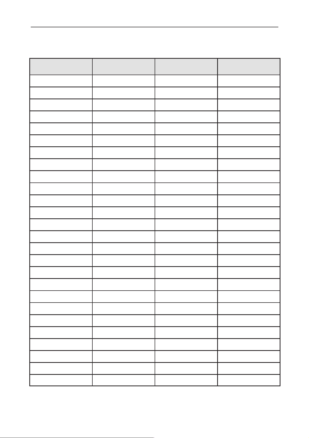
Figure 31. TX positive and negative I and Q signals signals should look like this (example is TXIN pin
21)
8 – 40
Original 03/98
Page 41

After Sales
RPE–1
Technical Documentation
Troubleshooting
Figure 32. MOD0 signal measured using Tektronix TDS 744 (pin 28).
Original 03/98
Figure 33. TX IF gain control (V103 pin 4).
8 – 41
Page 42

RPE–1
PAMS
Troubleshooting
Technical Documentation
Figure 34. TXC (for Power tuning coefficient 0.848), (C141 down).
8 – 42
Figure 35. TXGX (for tuning coefficient 0.848), (R120 right).
Original 03/98
Page 43

After Sales
RPE–1
Technical Documentation
Troubleshooting
Test RF mixer TX side
Table 10.
test point nominal tolerance notes
IF in L210 up –32 dBm 2 dB Spectrum analyzer settings:
FREQ 116 MHz, SPAN 10 MHz,
TRACE > Max hold
LO in V105 down –13 dBm 3 dB Spectrum analyzer settings:
FREQ 1018 MHz, SPAN 10 MHz,
RF out V104 pin 2
(lower right
hand corner)
–42 dBm 4 dB Spectrum analyzer settings:
FREQ 902 MHz, SPAN 10 MHz,
TRACE > Max hold
Test PA–driver
Table 11.
test point nominal tolerance notes
RF in N204 pin 1 (upper
left hand corner)
RF out N204 pin 4 (lower
right hand corner)
operating voltage 1 C249 up 2.8 V 0.2 V pulsed DC
operating voltage 2 N204 pin 6 2.8 V 0.2 V pulsed DC
–44 dBm 4 dB 902 MHz
–22 dBm 5 dB 902 MHz
Test TX RF SAW filter
Table 12.
test point nominal tolerance notes
RF in Z208 pin 2 –22 dBm 5 dB 902 MHz
RF out Z208 pin 5 –29 dBm 6 dB 902 MHz
Original 03/98
8 – 43
Page 44

RPE–1
PAMS
Troubleshooting
Test power control circuit
test point nominal tolerance notes
pwr control out
(APC)
reference in
(TXGX)
detected voltage C245 right 2.1 V
R254 up 3.1 V
see Figure 36
V201 pin 5 3.8 V
see Table 9 and
Figure 35.
see Figure 37.
Technical Documentation
Table 13.
1 V ’smooth pulse’,
duration 576 us
repetition 4.6 ms
1V ”
0.7 V ”
Figure 36. Typical APC voltage wave form to the PA at Power control level 7 (R254 up).
8 – 44
Original 03/98
Page 45

After Sales
RPE–1
Technical Documentation
Troubleshooting
Figure 37. Detected voltage from the power detector (V201 pin 5).
Test power amplifier
Table 14.
test point nominal tolerance notes
RF in C250 left –26 dBm 5 dB Spectrum analyzer settings:
FREQ 902 MHz, SPAN 10 MHz,
TRACE > Max hold
RF out C255 left +5 dBm 3 dB Spectrum analyzer settings:
FREQ 902 MHz, SPAN 10 MHz,
TRACE > Max hold, AMPLITUDE
20 dBm
operating voltage 1
operating voltage 2
C282 up 3.3 V 0.1 V DC (almost)
C208 up 3.3 V 0.1 V DC (almost)
Original 03/98
8 – 45
Page 46

RPE–1
PAMS
Troubleshooting
Technical Documentation
Test duplexer TX side
Table 15.
test point nominal tolerance notes
RF in Z106 pin 2 (TX) 4.5 dBm 2 dB Spectrum analyzer settings:
FREQ 902 MHz, SPAN 10 MHz,
TRACE > Max hold, AMPLITUDE
20 dBm
RF out Z106 pin 1
(ANT)
4.0 dBm 2 dB –”–
Check antenna switch
Make the connection and settings as on page 33.
Table 16.
test point nominal tolerance notes
RF in X71 common
port from duplexer
RF out X71 internal an-
tenna port
(spring)
3.7 dBm 2 dB Spectrum analyzer settings:
7 dBm 2 dB Spectrum analyzer settings: as
Synthesizer trouble shooting
Test equipment
– Service adapter JPT–8
– Cable DAU–9P
– Charger ACH–6E
– PC with WinTesla SW
– Security key PKD–1A
– Spectrum analyzer
FREQ 902 MHz, SPAN 10 MHz,
TRACE > Max hold, AMPLITUDE
20 dBm
above.
RF cable and attenuator removed.
8 – 46
– HF–probe 85024A
– Digital multimeter (e.g. Fluke 77 series II)
Test each block separately while the phone is in local mode, (TX active). Mea-
sure the LO and clock outputs using the Hewlett Packard HF–probe HP
85024A. Use the 10:1 adaptor (HP 11881A, which actually is a –20 dBm atten-
Original 03/98
Page 47

After Sales
RPE–1
Technical Documentation
uator). Measure the operating voltage using voltage meter and the control signals using either voltage meter or, in certain cases, oscilloscope.
Spectrum analyzer
Oscilloscope
HF probe
GX8
Charger
ACH–6E
JBT–8
PC
Troubleshooting
cable DAU–9P
PKD–1A
Figure 38. Synthesizer trouble shooting.
Settings
– WinTesla Testing > RF Controls > Active unit; TX, Opera-
tion mode Burst, Channel: 60, TX data type: Rand, TX
power level: 7.
– Service adapter: ’vertical mode’
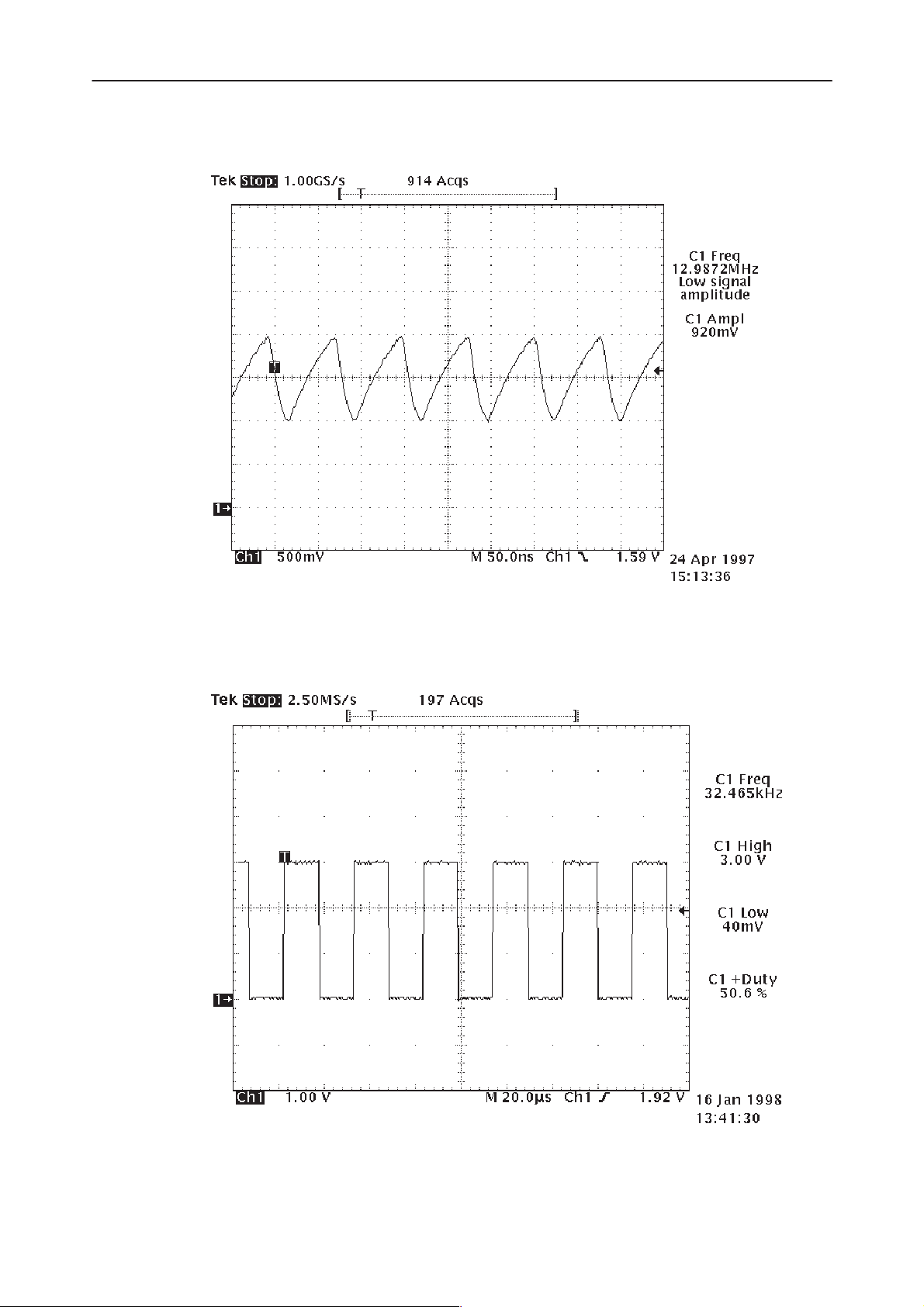
VCTCXO (G201)
Table 17.
test point nominal tolerance notes
control voltage C230 right 2.0 V 0.2 V DC
clock out R227 right 1.13 Vpp 0.3 V 13.000 MHz
operating voltage C218 left 4.5 V 0.3 V DC
voltage drop due to
operating current
V(R215 right) –
V(R215 left)
0.22 V 0.05 DC (1.2 mA)
Original 03/98
8 – 47
Page 48

RPE–1
PAMS
Troubleshooting
Technical Documentation
Figure 39. VCTCXO output at R227 right. (Toyocom)
UHF VCO (G200)
test point nominal tolerance notes
control voltage G200 pin1 (lower
right)
LO1 out G200 pin 4 (upper
left)
operating voltage G200 pin 3 (upper
right)
voltage drop due to
operating current
V(R204 right) –
V(R204 left)
Table 18.
2.2 V 0.3 V DC
–30 dBm (thru a 20
dB attenuator)
4.5 V 0.2 V DC
0.15 V 0.05 V DC (7 mA)
5 dB 1018 MHz (Easier
to measure in Con-
tinious Mode!)
8 – 48
Original 03/98
Page 49

After Sales
RPE–1
Technical Documentation
Troubleshooting
Figure 40. Control voltage of UHF VCO (pin 1 of G200)
UHF Buffer
test point nominal tolerance notes
operating voltage V105 down (collec-
tor)
voltage due to op-
erating current
RF in V105 upper right
RF out V105 down (collec-
R129 (left) –
R129(right)
(base), or R133 left
tor)
VHF VCO
test point nominal tolerance notes
Table 19.
2.9 V 0.5 V DC
1.5 V 0.3 V DC
–30.0 dBm 4 dB 1018 MHz
–11.5 dBm 4 dB 1018 MHz
Table 20.
control voltage V205 left 3.0 V 1 V DC
LO2 out C213 right –18 dBm 3 dB 232 MHz
operating voltage L200 right 4.56 V 0.2 V DC
voltage drop due to
operating current
V(R201 up) –
V(R201 down)
0.12 V 50 mV DC (5.5 mA)
Original 03/98
8 – 49
Page 50

RPE–1
PAMS
Troubleshooting
Technical Documentation
PLL IC (N202)
Table 21.
test point nominal tolerance notes
operating voltage1 C202 right 3.2 V 0.3 DC
operating voltage2 C205 right 3.3 V 0.3 DC
operating voltage of
charge pumps
data enable pin 13 see Figure 41 – pulsed
data pin 12 see Figure 41 – pulsed
data clocking pin 11 see Figure 41 – pulsed
pin 19 of N202 4.7 V 0.3 DC
Repair
SCLK
SDATA
SENA1
Figure 41.
Replace the broken component. Put on new covers. At least the extension box
should be new, because it wears out when the bottom cover is removed.
8 – 50
[]
Original 03/98
 Loading...