

Page 1

PAMS Technical Documentation
RPE–1 Series Transceiver
Chapter 3
SYSTEM MODULE
Original 02/98
Copyright 1998 Nokia Mobile Phones. All rights reserved
Page 2

RPE–1
PAMS
System Module
Amendment
Number
Technical Documentation
AMENDMENT RECORD SHEET
Date Inserted By Comments
Page 3–2
Original 02/98
Page 3

PAMS
RPE–1
Technical Documentation
CHAPTER 2 – TRANSCEIVER OVERVIEW
Contents
Introduction Page 3–6. . . . . . . . . . . . . . . . . . . . . . . . . . . . . . . . . . . . . . . . . . . .
Technical Summary Page 3–6. . . . . . . . . . . . . . . . . . . . . . . . . . . . . . . . . . .
Block Diagram of RF/System Module GX8 Page 3–6. . . . . . . . . . . . .
GSM functionality: Page 3–7. . . . . . . . . . . . . . . . . . . . . . . . . . . . . . . . . .
RF Section: Page 3–7. . . . . . . . . . . . . . . . . . . . . . . . . . . . . . . . . . . . . . .
Baseband: Page 3–7. . . . . . . . . . . . . . . . . . . . . . . . . . . . . . . . . . . . . . . .
Software Section: Page 3–8. . . . . . . . . . . . . . . . . . . . . . . . . . . . . . . . . .
Host control interface: Page 3–8. . . . . . . . . . . . . . . . . . . . . . . . . . . . . .
Audio interface: Page 3–8. . . . . . . . . . . . . . . . . . . . . . . . . . . . . . . . . . . .
Modes of Operation Page 3–8. . . . . . . . . . . . . . . . . . . . . . . . . . . . . . . . . . . . .
Standard PCMCIA mode: Page 3–8. . . . . . . . . . . . . . . . . . . . . . . . . . .
Vertical (i.e. non–PCMCIA) mode: Page 3–8. . . . . . . . . . . . . . . . . . . .
Operating Conditions Page 3–9. . . . . . . . . . . . . . . . . . . . . . . . . . . . . . .
External Signals and Connections Page 3–9. . . . . . . . . . . . . . . . . . . .
PCMCIA Connector Pinout Page 3–10. . . . . . . . . . . . . . . . . . . . . . . . . .
Antenna Connector Page 3–12. . . . . . . . . . . . . . . . . . . . . . . . . . . . . . . . .
SIM Connector Electrical Specifications Page 3–12. . . . . . . . . . . . . . .
System Module
Baseband Block Page 3–13. . . . . . . . . . . . . . . . . . . . . . . . . . . . . . . . . . . . . . . .
Introduction Page 3–13. . . . . . . . . . . . . . . . . . . . . . . . . . . . . . . . . . . . . . . . . .
Modes of Operation Page 3–13. . . . . . . . . . . . . . . . . . . . . . . . . . . . . . . .
Operating modes and interface signals of the RPE–1 Page 3–13.
Normal operation mode Page 3–14. . . . . . . . . . . . . . . . . . . . . . . . . . . . .
Flash programming mode Page 3–14. . . . . . . . . . . . . . . . . . . . . . . . . . .
Non–PCMCIA mode Page 3–14. . . . . . . . . . . . . . . . . . . . . . . . . . . . . . . .
Electrical Characteristics Page 3–15. . . . . . . . . . . . . . . . . . . . . . . . . . . . . .
Introduction Page 3–15. . . . . . . . . . . . . . . . . . . . . . . . . . . . . . . . . . . . . . .
Maximum Ratings Page 3–15. . . . . . . . . . . . . . . . . . . . . . . . . . . . . . . . . .
Supply Voltages and Power Consumption Page 3–15. . . . . . . . . . . . .
Operating Current (average values) Page 3–15. . . . . . . . . . . . . . . . . .
Block Diagram of RPE–1 Page 3–16. . . . . . . . . . . . . . . . . . . . . . . . . . . . . .
Interface specification Page 3–17. . . . . . . . . . . . . . . . . . . . . . . . . . . . . . .
RPE–1 interfaces Page 3–17. . . . . . . . . . . . . . . . . . . . . . . . . . . . . . . .
PCMCIA interface Page 3–17. . . . . . . . . . . . . . . . . . . . . . . . . . . . . . . . . .
SIM Interface Page 3–18. . . . . . . . . . . . . . . . . . . . . . . . . . . . . . . . . . . . . .
SIM Interface Signals Page 3–18. . . . . . . . . . . . . . . . . . . . . . . . . . . . .
SIM Connector Page 3–18. . . . . . . . . . . . . . . . . . . . . . . . . . . . . . . . . .
Baseband/RF interface Page 3–19. . . . . . . . . . . . . . . . . . . . . . . . . . . . .
Signals in MAD2 – RFI2 interface Page 3–19. . . . . . . . . . . . . . . . . .
SMART – MAD2 interface Page 3–20. . . . . . . . . . . . . . . . . . . . . . . . . . .
Original 02/98
Page 3–3
Page 4

RPE–1
PAMS
System Module
SMART – MAD2 Interface Signals Page 3–20. . . . . . . . . . . . . . . . .
MBUS interface Page 3–20. . . . . . . . . . . . . . . . . . . . . . . . . . . . . . . . . . . .
Memory interface Page 3–21. . . . . . . . . . . . . . . . . . . . . . . . . . . . . . . . . .
Memory Interface Signals Page 3–21. . . . . . . . . . . . . . . . . . . . . . . . .
Memory Interface Signals Page 3–22. . . . . . . . . . . . . . . . . . . . . . . . .
Functional Description Page 3–22. . . . . . . . . . . . . . . . . . . . . . . . . . . . . . . .
Power Distribution Tree Page 3–23. . . . . . . . . . . . . . . . . . . . . . . . . . .
Power Distribution Block Diagram Page 3–24. . . . . . . . . . . . . . . . . . . .
Power–up scheme Page 3–25. . . . . . . . . . . . . . . . . . . . . . . . . . . . . . . . .
Power–up sequence Page 3–25. . . . . . . . . . . . . . . . . . . . . . . . . . . . .
Power–up In PCMCIA mode Page 3–25. . . . . . . . . . . . . . . . . . . . . . . . .
Power–up In Non–PCMCIA mode Page 3–26. . . . . . . . . . . . . . . . . . . .
Power–down Scheme Page 3–26. . . . . . . . . . . . . . . . . . . . . . . . . . . . . .
Clocking Page 3–27. . . . . . . . . . . . . . . . . . . . . . . . . . . . . . . . . . . . . . . . . . . . .
Reset Page 3–28. . . . . . . . . . . . . . . . . . . . . . . . . . . . . . . . . . . . . . . . . . . . .
Sleep mode Page 3–28. . . . . . . . . . . . . . . . . . . . . . . . . . . . . . . . . . . . . . .
RF Block Page 3–29. . . . . . . . . . . . . . . . . . . . . . . . . . . . . . . . . . . . . . . . . . . . . . .
Introduction Page 3–29. . . . . . . . . . . . . . . . . . . . . . . . . . . . . . . . . . . . . . . . . .
Frequency Plan Page 3–29. . . . . . . . . . . . . . . . . . . . . . . . . . . . . . . . . . . .
Maximum Ratings Page 3–30. . . . . . . . . . . . . . . . . . . . . . . . . . . . . . . . . .
DC Characteristics Page 3–30. . . . . . . . . . . . . . . . . . . . . . . . . . . . . . . . . . . .
Power Distribution Diagram Page 3–30. . . . . . . . . . . . . . . . . . . . . . . . . .
Regulators Page 3–31. . . . . . . . . . . . . . . . . . . . . . . . . . . . . . . . . . . . . . . .
Control Signals Page 3–31. . . . . . . . . . . . . . . . . . . . . . . . . . . . . . . . . . . .
RF Characteristics Page 3–31. . . . . . . . . . . . . . . . . . . . . . . . . . . . . . . . .
TX Characteristics Page 3–31. . . . . . . . . . . . . . . . . . . . . . . . . . . . . . . . . .
Functional Description Page 3–32. . . . . . . . . . . . . . . . . . . . . . . . . . . . . . . .
Receiver Page 3–32. . . . . . . . . . . . . . . . . . . . . . . . . . . . . . . . . . . . . . . . . .
Synthesizer Page 3–33. . . . . . . . . . . . . . . . . . . . . . . . . . . . . . . . . . . . . . .
Transmitter Page 3–33. . . . . . . . . . . . . . . . . . . . . . . . . . . . . . . . . . . . . . . .
Transmitter Power Budget. From PA to Antenna Page 3–34. . . . .
Block Diagram of GX8 RF section Page 3–35. . . . . . . . . . . . . . . . . . . .
RF Characteristics Page 3–36. . . . . . . . . . . . . . . . . . . . . . . . . . . . . . . . . . . .
Receiver Page 3–36. . . . . . . . . . . . . . . . . . . . . . . . . . . . . . . . . . . . . . . . . .
Duplex filter Page 3–36. . . . . . . . . . . . . . . . . . . . . . . . . . . . . . . . . . . . . . .
Low noise amplifier Page 3–37. . . . . . . . . . . . . . . . . . . . . . . . . . . . . . . . .
RF RX Filter Page 3–37. . . . . . . . . . . . . . . . . . . . . . . . . . . . . . . . . . . . . . .
RF mixer Page 3–38. . . . . . . . . . . . . . . . . . . . . . . . . . . . . . . . . . . . . . . . . .
IF amplifier Page 3–38. . . . . . . . . . . . . . . . . . . . . . . . . . . . . . . . . . . . . . . .
1st–IF filter Page 3–38. . . . . . . . . . . . . . . . . . . . . . . . . . . . . . . . . . . . . . . .
Receiver IF circuit, RX part of CRFRT Page 3–39. . . . . . . . . . . . . . . .
2nd–IF filter Page 3–40. . . . . . . . . . . . . . . . . . . . . . . . . . . . . . . . . . . . . . .
Transmitter Page 3–40. . . . . . . . . . . . . . . . . . . . . . . . . . . . . . . . . . . . . . . . . .
Modulator circuit, TX part of the CRFRT Page 3–41. . . . . . . . . . . . . . .
Technical Documentation
Page 3–4
Original 02/98
Page 5

PAMS
RPE–1
Technical Documentation
RF TX mixer Page 3–42. . . . . . . . . . . . . . . . . . . . . . . . . . . . . . . . . . . . . . .
PA–driver amplifier Page 3–42. . . . . . . . . . . . . . . . . . . . . . . . . . . . . . . . .
RF TX filter Page 3–42. . . . . . . . . . . . . . . . . . . . . . . . . . . . . . . . . . . . . . . .
Power amplifier Page 3–43. . . . . . . . . . . . . . . . . . . . . . . . . . . . . . . . . . . .
Power control circuit Page 3–44. . . . . . . . . . . . . . . . . . . . . . . . . . . . . . . .
Synthesizer Page 3–44. . . . . . . . . . . . . . . . . . . . . . . . . . . . . . . . . . . . . . . . . .
Crystal oscillator Page 3–44. . . . . . . . . . . . . . . . . . . . . . . . . . . . . . . . . . .
VHF PLL Page 3–45. . . . . . . . . . . . . . . . . . . . . . . . . . . . . . . . . . . . . . . . . .
VHF VCO + buffer Page 3–45. . . . . . . . . . . . . . . . . . . . . . . . . . . . . . . . . .
UHF PLL Page 3–46. . . . . . . . . . . . . . . . . . . . . . . . . . . . . . . . . . . . . . . . . .
UHF VCO Page 3–46. . . . . . . . . . . . . . . . . . . . . . . . . . . . . . . . . . . . . . . . .
UHF Buffer Page 3–47. . . . . . . . . . . . . . . . . . . . . . . . . . . . . . . . . . . . . . . .
PLL Integrated Circuit Page 3–47. . . . . . . . . . . . . . . . . . . . . . . . . . . . . . .
Connections Page 3–48. . . . . . . . . . . . . . . . . . . . . . . . . . . . . . . . . . . . . . . . .
Antenna connector Page 3–48. . . . . . . . . . . . . . . . . . . . . . . . . . . . . . . . .
RF/Baseband connections Page 3–48. . . . . . . . . . . . . . . . . . . . . . . . . .
Timings Page 3–52. . . . . . . . . . . . . . . . . . . . . . . . . . . . . . . . . . . . . . . . . . . . .
Supply power control timing diagrams Page 3–52. . . . . . . . . . . . . . . . .
Synthesizer control timing diagrams Page 3–53. . . . . . . . . . . . . . . . . .
Transmitter power switching timing diagram Page 3–54. . . . . . . . . . .
System Module
Parts list of GX8 baseband and RF module Page 3–55. . . . . . . . . . . . . . . . .
Schematic Diagrams:
Block Diagram of System/RF Blocks (Version 3.0 Edit 57) 3/A3–1. . .
Circuit Diagram of System Connectors (Version 3.0 Edit 16) 3/A3–2
Circuit Diagram of ASIC and Power Handling (Version 3.0 Edit 21) 3/A3–3
Circuit Diagram of Memory Blocks (Version 2.97 Edit 16) 3/A3–4
Circuit Diagram of RFI (Version 2.97 Edit 10) 3/A3–5. . . . . . . . . . . . . .
Circuit Diagram of RF/TX Connections (Version 3.0 Edit 51) 3/A3–6
Circuit Diagram of Receiver (Version 2.97 Edit 27) 3/A3–7. . . . . . . . .
Circuit Diagram of Transceiver (Version 3.0 Edit 25) 3/A3–8. . . . . . . .
Layout Diagram of GX8 (Version 18) 3/A3–9. . . . . . . . . . . . . . . . . . . . . .
Original 02/98
Page 3–5
Page 6
RPE–1
PAMS
System Module
Introduction
The Cellular Card Phone RPE–1 is a GSM class 5 compatible cellular phone
without a battery or user interface of its own. Instead, the device is computer
controlled through the 68–pin PCMCIA connector. This connector is used to:
– 1) supply the card with all operating power it needs
– 2) transfer operating commands and their responses,
– 3) transfer digitized speech or GSM data and control messages and
– 4) during production or servicing transfer tuning parameters and FLASH
download data.
Physically the RPE–1 is compatible with the PC Card ’95 standard
(and earlier PCMCIA standard) for type II extended cards.
Technical Summary
The Nokia Cellular Card Phone RPE–1 hardware comprises four basic func-
tional blocks:
Technical Documentation
– 1) Rotatable Helix antenna
– 2) RF, a low power and low profile derivative from DCT2 (HD843)
– 3) BB, mixed DCT2 (RFI2) and DCT3 (MAD2)
– 4) Host interface/system control through RPE–1 specific ASIC ”SMART”
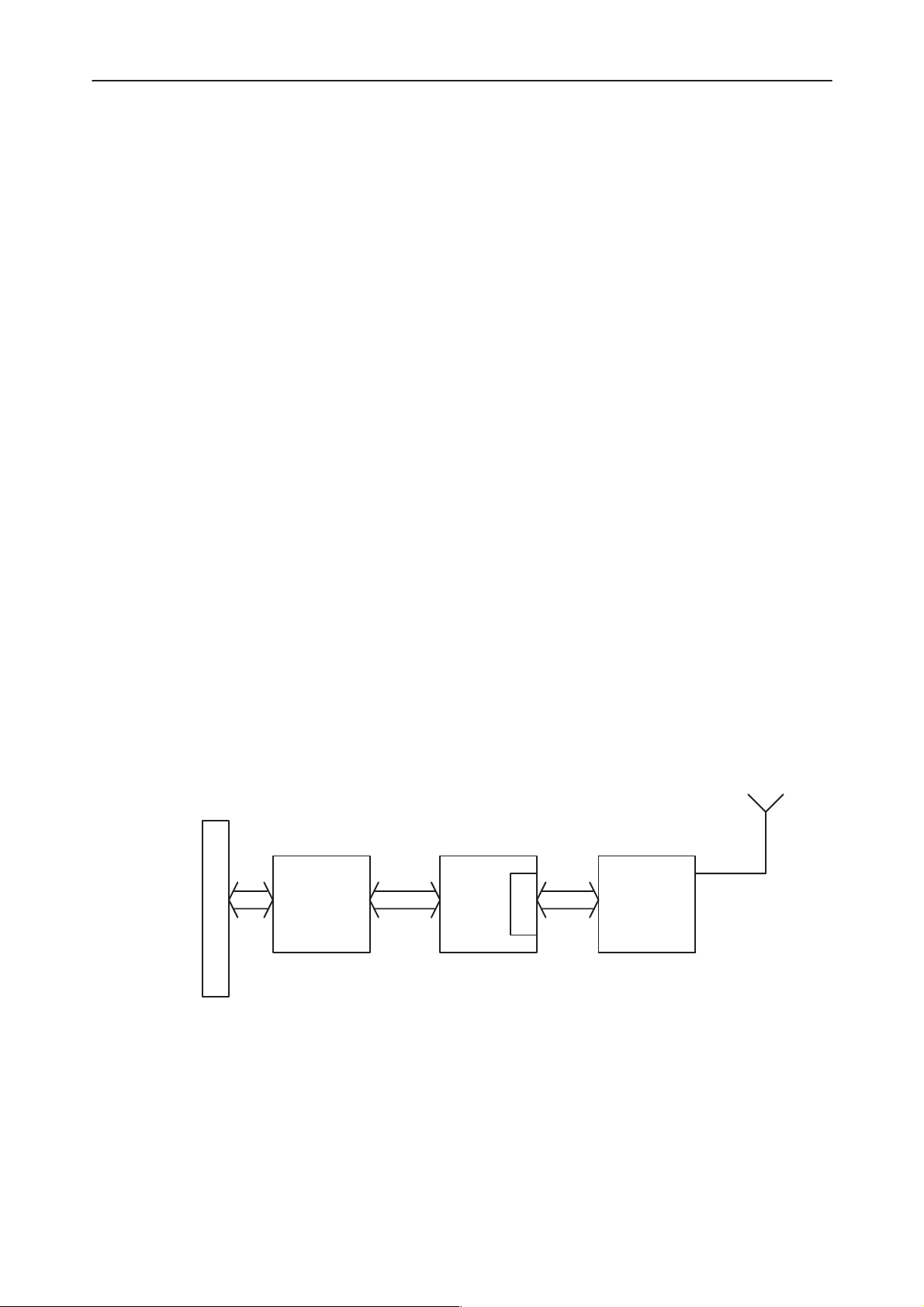
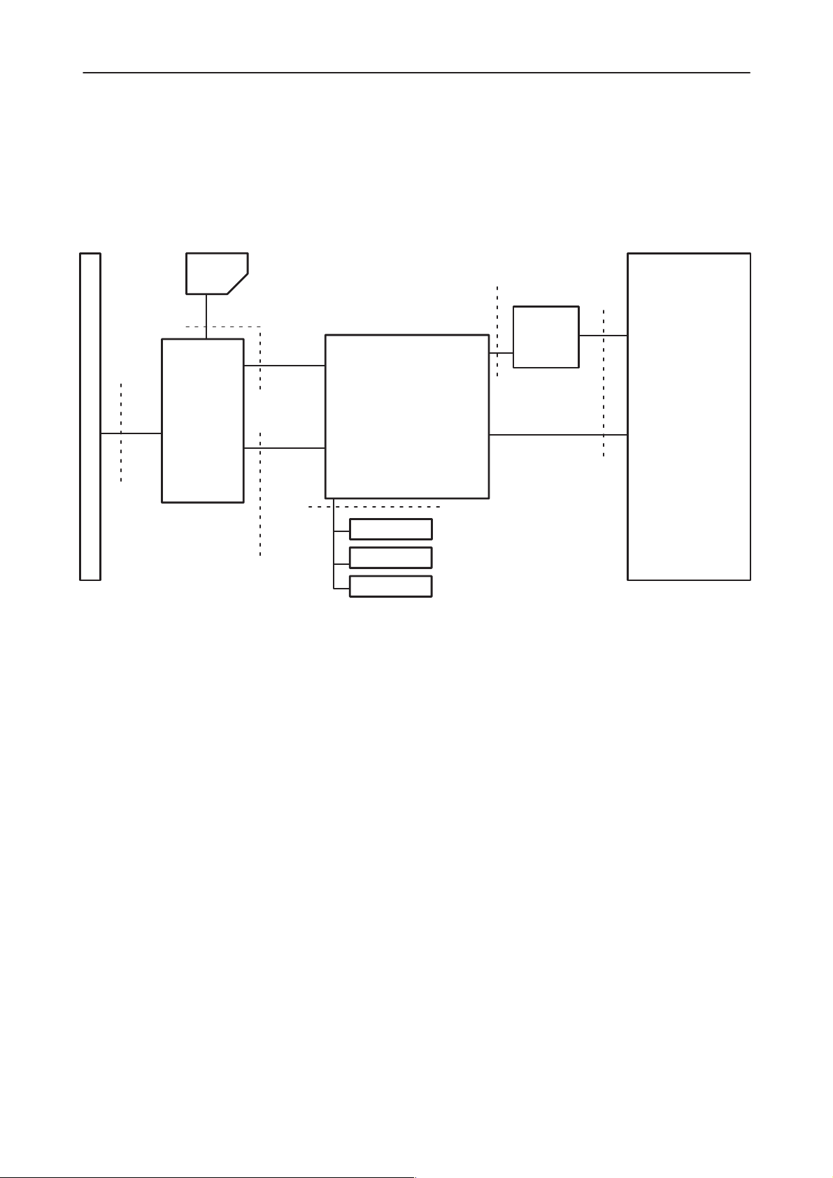
Block Diagram of RF/System Module GX8
PCMCIA CONN
SMART
ASIC
Parellel
8–bit memory
interface
FBUS
MBUS
PCM audio
I/O:s
BB RF
Antenna
RFI2
Page 3–6
Original 02/98
Page 7
PAMS
RPE–1
Technical Documentation
GSM functionality:
The RPE–1 is a GSM phase I type approved cellular telephone with maximum
output power of 0.8W (power class 5). The following GSM services are sup-
ported:
– voice,
– non–transparent and transparent data,
– fax
– SMS.
RF Section:
The RPE–1 interfaces to its surroundings through a rotatable helix antenna.
Alternatively, the helix can be removed and a plug for an external antenna in-
serted instead. Because the RPE–1 antenna connector is Nokia specific, a
dedicated external antenna cable with a standard FME–connector at the other
end must to be used.
The power amplifier is optimized for use at 3.3V supply voltage. Voltages up to
5.25V voltages are accepted, but excessive heat is generated.
System Module
Baseband:
The baseband consists of three ASICs: MAD2 system control ASIC, SMART
PCMCIA interface ASIC and DCT2 based BB/RF interface ASIC RFI2. The
baseband is basically similar as DCT3 baseband, differences are in powering
and added interface to host computer via SMART ASIC and a PCMCIA connec-
tor.
The baseband performance is optimal at 3.3V supply voltage. Higher supply
voltage up to 5.25V are usable, but excessive heat is generated.
Baseband memory mapping is shown below.
0010 0000
001F FFFF
MCUADDR
(0:19)
MCUDATA
(0:15)
SRAM
FLASH
0020 0000
005F FFFF
Original 02/98
EEPROM
DATA
Serial
EEPROMMAD2
00A0 0000
00DF FFFF
Page 3–7
Page 8

RPE–1
PAMS
System Module
Software Section:
The RPE–1 includes MCU (Main Control Unit) software and DSP (Digital Signal
Processing) Software. MAD2 ASIC contains MCU processor (ARM) and DSP
processor (LEAD). MCU and DSP softwares are based on DCT3 GSM soft-
ware packages. Internal data functionality has been added on RPE–1 soft-
ware.
Host control interface:
This interface is a standard PCMCIA card interface, which is based on PC Card
’95 release.
Audio interface:
The audio interface is handled by the host computer audio interface (voice
card, speaker/headphones and microphone). Kindly refer to the audio specifi-
cation.
Technical Documentation
Modes of Operation
Standard PCMCIA mode:
This is the standard operating mode of the RPE–1. The card is used as a stan-
dard 8–bit PCMCIA I/O device. The host PC automatically configures its inter-
nal memory and interrupt mapping based on so called CIS (Configuration In-
formation Structure, specified in PC Card ’95 standard ) memory contents
stored inside the SMART ASIC within the RPE–1 baseband.
The RPE–1 is controlled through a number of memory mapped registers. The
digital audio interface is supported through a dedicated FIFO buffered memory
locations.
Vertical (i.e. non–PCMCIA) mode:
For host devices not having a free PCMCIA slot the RPE–1 has been designed
to support also direct serial bus operation. In this mode the PCMCIA connector
is no longer literally a PCMCIA connector, but a number of connector signals
have been redefined to support new logical interfaces.
The typical RPE–1 host interface is RS232C. The application specific socket
for the Cellular Card Phone is assumed to contain all 3.3V to RS232C buffering
circuitry, a 3.3V max. 1A supply regulator and a system RESET generator.
Should also voice calls be required in the application, the related codec and
analog amplifying circuitry would become essential as well.
Page 3–8
The vertical operating mode is activated by grounding pin 62 (SPKR#/BVD2) in
the PCMCIA connector before card RESET is released. Pin 62 (SPKR#/BVD2)
must be kept grounded all the time when operating in non–PCMCIA mode.
Original 02/98
Page 9
PAMS
RPE–1
Technical Documentation
System Module
The SPKR#/BVD2 pin has an internal pull–up resistor ensuring standard
PCMCIA mode operation if the pin is left unconnected.
Operating Conditions
Symbol Parameter Min. Typical Max. Unit Comments
V
cc
I
cc
V
pp
V
pplk
I
pp
V
I
V
O
V
IH
V
IL
V
OH
V
OL
I
IL
I
IH
I
OZ
t
t
T
A
Input voltage, PCMCIA conn. 0 V
Output voltage, PCMCIA conn. 0 V
Supply voltage 3.0 3.3 5.25 V PCMCIA Vcc
Supply current 700 mA
Programming voltage 2.7 3.6 V Generated internally
Vpp lockout voltage 0 1.5 V Erase & write inhib-
ited when Vpp=Vpplk
Programming current 0.0002 0.002 40 mA Typical: Read current
when Vpp=3V
CC
CC
V
V
High level input voltage 2 V
Low level input voltage 0.8 V
High level output voltage 0.7VCC VCC V IOH=Rated (9.7 mA)
Low level output voltage 0 0.2VCC V IOL=Rated (9.7 mA)
Low level input current –1 uA VI=GND
High level input current 1 uA VI=Vcc
High impedance output curr. –10 10 uA VI=Vcc or GND
input transition (rise/fall) 0 25 ns
Operational ambient
temperature range
–20 55 C Customer informa-
tion (GSM Phase I)
External Signals and Connections
Table 1. List of Connectors
Connector Name Code Notes Specifications / Ratings
PCMCIA connector 5469079 3.3V and 5V PCMCIA slots
SIM connector 5409063 GSM Phase I SIM connector
External antenna cable con-
nector
5429009
Original 02/98
Page 3–9
Page 10

RPE–1
PAMS
System Module
Technical Documentation
PCMCIA Connector Pinout
Pin Signal/
PCMCIA
1 GND GND
2 D3 MAD VCXOEna in/out out
3 D4 RI in/out out
4 D5 DCD in/out out
5 D6 CTS in/out out
6 D7 PCMTxData in/out out
7 CE1# Unused in 10k pull up resistor in RPE–1
8 A10 Unused Not connected
9 OE# Unused in 10k pull up resistor in RPE–1
10 A11 Unused Not connected
11 A9 Unused Not connected
12 A8 SMART SleepClkEn
13 A13 Unused Not connected
Signal/NON–PCMCIA Dir/
PCMCIA
in In In NON–PCMCIA mode DO NOT
External pull down
Dir/NON–
PCMCIA
Comments
LEAVE FLOATING!
14 A14 Unused Not connected
15 WE# Unused in In 10k pull up resistor in RPE–1
16 IREQ# Unused out
17 VCC1 VCC1 in in
18 VPP1 Unused Not connected
19 A16 Unused Not connected
20 A15 Unused Not connected
21 A12 Unused Not connected
22 A7 MAD FBUSTxData in out FBUSTxD
23 A6 MAD FBUSRxData in in FBUSRxD
24 A5 DTR in in
25 A4 RTS in in
26 A3 MAD PCMSClk in in
27 A2 MAD PCMDClk in in
28 A1 MAD PCMRxData in in
29 A0 MAD MBUS
External pull up
30 D0 Logic low (not used) in/out out
in in/out DO NOT LEAVE FLOATING!
MBUS low in startup initiates flashing.
31 D1 Logic low (not used) in/out out
32 D2 Logic low (not used) in/out out
33 IOIS16# Unused out Directly connected to VCC in RPE–1
34 GND GND
Page 3–10
Original 02/98
Page 11
PAMS
RPE–1
Technical Documentation
Pin
PCMCIA
35 GND GND
36 CD1# Unused out Directly grounded in RPE–1
37 D11 Unused Not connected
38 D12 Unused Not connected
39 D13 Unused Not connected
40 D14 Unused Not connected
41 D15 Unused Not connected
42 CE2# Unused in 10k pull up resistor in RPE–1
43 VS1# Unused Not connected
44 IORD# Unused in 10k pull up resistor in RPE–1
45 IOWR# Unused in 10k pull up resistor in RPE–1
46 A17 Unused Not connected
47 A18 Unused Not connected
48 A19 Unused Not connected
Signal/NON–PCMCIASignal/
Dir/
PCMCIA
PCMCIA
CommentsDir/NON–
System Module
49 A20 Unused Not connected
50 A21 Unused Not connected
51 VCC2 VCC2 in in
52 VPP2 Unused Not connected
53 A22 Unused Not connected
54 A23 Unused Not connected
55 A24 Unused Not connected
56 A25 Unused Not connected
57 VS2# Unused Not connected
58 RESET RESET in in 100k pull up resistor in RPE–1
59 WAIT# Unused Not connected
60 INPACK# Unused out
61 REG# Unused in 10k pull up resistor in RPE–1
62 SPKR#/
BVD2
63 STSCHG# Unused Not connected
64 D8 Unused Not connected
65 D9 Unused Not connected
SMART internal
op. mode sel
in in LOW for NON–PCMCIA mode. 10k
pull up resistor in RPE–1
66 D10 Unused Not connected
67 CD2# Unused out Directly grounded in RPE–1
68 GND GND
Original 02/98
Page 3–11
Page 12
RPE–1
PAMS
System Module
Technical Documentation
Antenna Connector
Pin Line
Symbol
X71 RFOUT Impedance 50 Ω at 890...960 MHz
Parameter Mini-
mum
Typical
/ Nomi-
nal
Maxi-
mum
Unit / Notes
SIM Connector Electrical Specifications
Pin Name Parameter Min Typ Max Unit Notes
4 GND GND 0 0 V Ground
3, 5 VSIM 5V SIM Card 4.8 5.0 5.2 V Supply voltage
6 SIMDA-TA5V Vin/Vout 4.0
0
2 SIMRST 5V SIM Card 4.0 HIGH VSIM V SIM reset
HIGH
LOW
VSIM
0.5
V SIM data
Trise/Tfall max 1us
1 SIMCLK Frequency
Trise/Tfall
3.25
25
MHz
ns
SIM clock
Page 3–12
Original 02/98
Page 13
PAMS
RPE–1
Technical Documentation
Baseband Block
Introduction
This document specifies the BB section of the GX8 RF/system module for
RPE–1 Transceiver Card The BB section of the GX8 employs the MAD2 ASIC
from DCT–3, RFI2 (RF/BB interface ASIC) from DCT–2, and a new ASIC
named as SMART to interface to a PCMCIA slot, and to a GSM phase I SIM
reader. The main guideline for the baseband block is the PC Card ’95 release,
which contains considerable hardware and software enhancements compared
to the earlier versions of the PCMCIA standard. Another important set of proposals is included in the ExCA specification that provides a more narrow definition of PC Card technology for PC architecture machines. The current revision
of the ExCA standard is Release 1.50 .
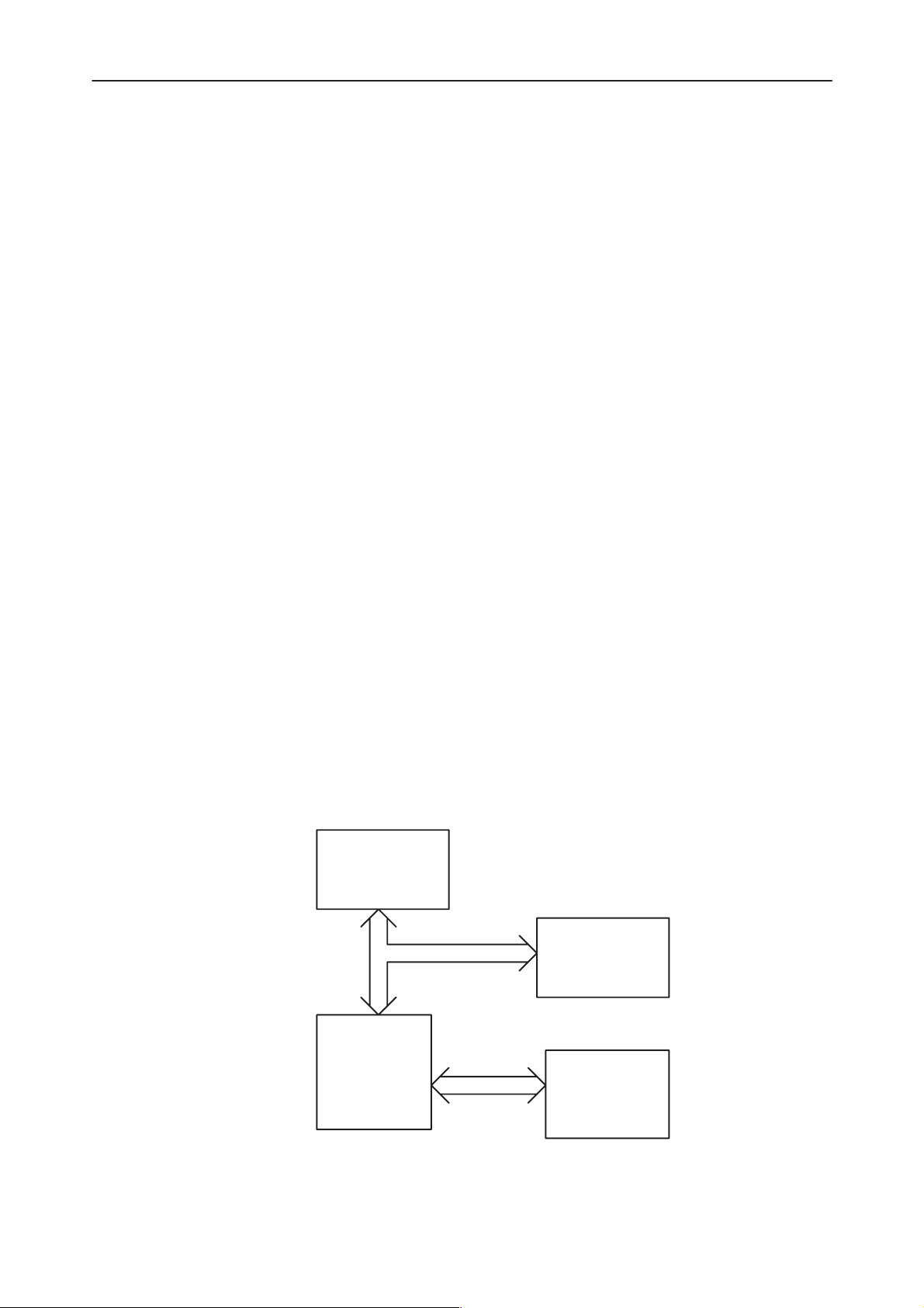
Modes of Operation
The Baseband in RPE–1 operates in one of the several operating modes. All
modes except one are normal PCMCIA modes. One mode is for use in non–
PCMCIA environments. The diagram below presents both physical operating
and logical sub operating modes.
System Module
RPE–1 can be used in systems where standard PCMCIA host controller is not
available. In non–PCMCIA mode the PCMCIA interface is bypassed inside the
interface ASIC so that the MBUS, FBUS and PCM speech data signals are
brought directly to the PCMCIA connector.
Operating modes and interface signals of the RPE–1
RPE–1
PCMCIA MODE Non–PCMCIA MODE
NORMAL MODE
–Memory mode: CIS
–I/O mode:
–PCM speech
–FBUS
FLASH PRG MODE DAI MODE
–MBUS (Flash clk)
–FBUS
–FBUS (to DAI box)
–PCM speech
NOKIA PROPRIETARY MODE
–FBUS
–PCM speech
–MBUS
–RESET
–Flow control signals
Original 02/98
Page 3–13
Page 14

RPE–1
PAMS
System Module
Normal operation mode
In the normal operating mode the RPE–1 acts as a cellular telephone without
built–in UI. After power–up the PCMCIA interface is first in memory mode, during which the host computer reads the PC CARD standard CIS information
from the RPE–1 card. The CIS is stored in the internal ROM of the SMART
interface ASIC. After reading the CIS the interface goes into I/O mode for runtime operation. One bit in the SMART operation control register determines
which mode is being used.
In normal operation the card looks like a modem card to the host computer. The
operation interface emulates a 16C550 UART. Control data for the RPE –1
goes through the UART to the internal FBUS of system ASIC MAD2. In addition there is an USRT through which speech data flows. It has its own control
and data registers in the interface ASIC. All this is implemented in the SMART
ASIC.
Flash programming mode
The Flash programming mode is used in updating the card software. The host
computer and the RPE–1 control software in it control the Flash download procedure.
Technical Documentation
During Flash programming the FBUS operates in synchronous mode with the
MBUS signal acting as a clock. The data to be downloaded to the RPE–1 goes
through the FBUS. The SMART ASIC generates the clock. The Flash mode is
selected with a bit in SMART operation mode control register.
Non–PCMCIA mode
RPE–1 can be used in applications where standard PCMCIA interface is not
available. Non–PCMCIA mode offers a simple interface for controlling it. The
controller thus does not have to be a personal computer but a simple microcontroller is enough.
Non–PCMCIA mode is activated by connecting pin ”BVD2/SPKR#” to the
ground on the host side of the PCMCIA connector. When this signal is 0 the
interface ASIC enters the non–PCMCIA mode and routes FBUS, flow control
signals and PCM speech data bus directly to the PCMCIA connector. Also A8
should be pulled down with 100k resistor to enable SMART ASIC sleep clock
feature. Internal registers of the interface ASIC are not accessible, so the ASIC
takes care of proper startup of the card. The external system must give a proper RESET signal.
In the non–PCMCIA mode MBUS is routed via a bidirectional switch directly to
the PCMCIA connector pin 29 A0. This switch is controlled by BVD2/SPKR#.
This allows user to control MAD2 with MBUS.
Page 3–14
Original 02/98
Page 15
PAMS
RPE–1
Technical Documentation
Electrical Characteristics
Introduction
The RPE–1 supply voltage must be in the range of 3.0 V to 5.25V. There is a
special undervoltage sensing supervisor circuit for stopping the Card if VCC
goes below the nominal 2.93V ( 2.92– 2.96V for the whole temperature range).
If the voltage goes below this value, SimCardDetX is driven LOW and power–
down sequence starts.
Maximum Ratings
Symbol Parameter Ratings Unit Comments
V
V
V
I
I
CC
I
o
IK
OK
Supply voltage –0.5 to 5.5 V see the next table below.
Input voltage range –0.5 to VCC+0.5 V
Output voltage range –0.5 to VCC+0.5 V
Input clamp current 20 mA
Output clamp current 20 mA
Operating temperature range –25 to +70 °C
Storage temperature range –40 to +85 °C
System Module
Supply Voltages and Power Consumption
Pin / Conn. Line Symbol Minimum Typical / Nomi-
nal
17 PCMCIA connector supply
voltage VCC
51 PCMCIA connector supply
voltage VCC
17 PCMCIA connector supply
current VCC
51 PCMCIA connector supply
current VCC
3.0V 3.3V 5.25V
3.0V 3.3V 5.25V
Operating Current (average values)
Operating voltage (V) Operating mode Total (mA)
3.3 idle 32
3.3 call 301
3.3 reset 5
Maximum
500mA
500mA
Original 02/98
Page 3–15
Page 16
RPE–1
PAMS
System Module
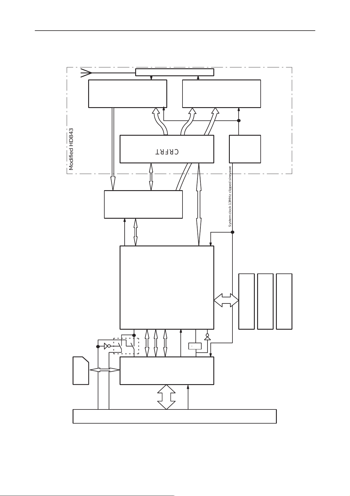
Block Diagram of RPE–1
RX
Modified HD843 RF block
RXIP, RXIN
AFC
RFI2
CRFRT
TXQP , TXQN
TXIP , TXIN,
Technical Documentation
Duplex filter
TX
VCTCXO
CRFRT cntrl
SIM
SIM data, 5V
RFI cntrl
CLK 13MHz
MBUS
SIM data
FBUS
MAD2
PCM speech
SleepCLK
SMART
PURX
Delay
SIMCardDetX
System clock 13MHz clipped sinevawe
Memory bus
SRAM
FLASH
EEPROM
Page 3–16
SPKR#/BVD2
A0 pin 29
Pin 62
PCMCIA bus
RESET
PCMCIA connector
Original 02/98
Page 17
PAMS
RPE–1
Technical Documentation
Interface specification
RPE–1 interfaces
SIM
SIM interface
PCMCIA
PCMCIA interface
PCMCIA conn. 68 pin
Interface
ASIC
SMART
MAD2–RFI2 interface
System ASIC
MAD2
System Module
RF block
RFI2
BB–RF interface
SMART–MAD2 interface
PCMCIA interface
All digital activity to external hosts go through the PCMCIA interface. This interface is handled by the SMART ASIC. In the SMART ASIC the PCMCIA interface section VCC is the PCMCIA connector VCC. The SMART ASIC uses
three independent supply voltages:
– for SIM interface VSIM supply,
– for PCMCIA interface VCC supply and
– for SMART ASIC core VCCARD supply.
The interface has two operating modes: one for PCMCIA compliant computer
hosts and one for non–PCMCIA hosts. Pin definitions depend on the mode.
The PCMCIA interface has two different pinouts. The first is the normal
PCMCIA pinout which conforms to the PC Card ’95 standard. The second
mode is the Nokia proprietary mode in which FBUS and PCM SIO buses are
connected directly to the PCMCIA connector. Also flow control signals, RESET,
and MBUS are routed to the connector. MBUS is used for synchronizing the
FBUS during data transfer in FLASH–mode. The PCMCIA connector pinouts
and corresponding electrical characteristics are listed in the next table.
Memory interface
SRAM
EEPROM
Flash
Original 02/98
Page 3–17
Page 18
RPE–1
Explanation
Explanation
PAMS
System Module
Technical Documentation
SIM Interface
The SIM card connector is located in the baseband section. The system ASIC
MAD2 controls the SIM card. All signals go through the interface ASIC SMART
for level conversion.
While the baseband block operates on 3.0 V supply, phase I SIM cards require
a 5 V operating voltage. Level conversion for the signals is done in the interface
ASIC SMART. The I/O cells of the SMART for the SIM signals have a separate
5 V power supply. SIM signals are listed in the table below. All SIM signals
must be able to withstand short circuit to ground without damage.
SIM Interface Signals
SIM card SMART
Pin name Direction Pin name Direction
VSIM VSIM SIM card operating voltage.
GND GND
SIMRST IN SRstOut OUT SIM RESET.
SIM ground. Connected to common
ground of the phone.
SIMCLK IN SClkOut OUT SIM clock.
SIMDATA I/O SDataS I/O SIM data.
SMART MAD2
Pin name Direction Pin name Direction
SRstInX IN SIMCardRstX OUT SIM RESET from MAD2
SClkin IN SIMCardClk OUT SIM clock from MAD2
SDataM I/O SIMCardData I/O SIM data to/from MAD2
SIOCIn IN SIMCardIOC OUT
SIMCardPwr OUT SIM power control.
SIM data direction control from MAD2.
When LOW data flow. MAD2 –> SMART
SIM Connector
Pin Name Parameter Min Typ Max Unit Notes
4 GND GND 0 0 V Ground
3, 5 VSIM 5V SIM Card 4.8 5.0 5.2 V Supply voltage
6 SIM
DATA
5V Vin/Vout 4.0
0
HIGH
LOW
VSIM
0.5
V SIM data
Trise/Tfall max 1us
2 SIMRST 5V SIM Card 4.0 HIGH VSIM V SIM reset
1 SIMCLK Frequency
Trise/Tfall
3.25
25
MHz
ns
SIM clock
Page 3–18
Original 02/98
Page 19
PAMS
Explanation
I/O
I/O
RFI2 data bus
OUT
IN
RFI2 address bus
RPE–1
Technical Documentation
Baseband/RF interface
Signals between the system ASIC MAD2 and RFI2 ASIC are digital signals and
thus are not in the scope of the RF specification. Signals in the MAD2–RFI2 interface are listed in the following table.
Signals in MAD2 – RFI2 interface
MAD2 RFI2
Pin name Direction Pin name Direction
COBBAClk OUT RFICLK IN System clock for RFI2.
VCXOPwr OUT
COBBADa0 RFIDA0
COBBADa1 RFIDA1
COBBADa2 RFIDA2
COBBADa3 RFIDA3
RFI2. analog power control. Connected to
RFI2 regulator.
System Module
COBBADa4 RFIDA4
COBBADa5
COBBADa6
COBBADa7 RFIDA7
COBBADa8 RFIDA8
COBBADa9 RFIDA9
COBBADa10 RFIDA10
COBBADa11 RFIDA11
COBBAAd0 RFIAD0
COBBAAd1
COBBAAd2
COBBAAd3 RFIAD3
COBBARdX OUT RFIRDX IN RFI2 read select.
COBBAWrX OUT RFIWRX IN RFI2 write select.
COBBADAX IN RFIDAX OUT RFI2 data available acknowledge.
IN RFIDAAUX OUT RFI2 auxiliary data available acknowledge.
DSPGENOUT5 OUT SYSRESETX IN RFI2 reset.
RFIDA5
.
RFIDA6
RFIAD1
.
RFIAD2
Original 02/98
Page 3–19
Page 20
RPE–1
Explanation
PAMS
System Module
Technical Documentation
SMART – MAD2 interface
The interface between the SMART and MAD2 ASICs is basically an asynchronous FBUS and a synchronous PCM bus. These serial buses are common for
all DCT3 phones. FBUS is there for transferring the control data between the
host computer and the system ASIC MAD2. The PCM bus transfers only
speech samples during a voice call. In normal phone speech samples would
go to speech codec.
The interface contains also the system RESET. The SIM interface is another
part of SMART–MAD2 interface.
SMART – MAD2 Interface Signals
SMART MAD2
Pin name Direction Pin name Direction
FBusTxD OUT AccRxData IN FBUS data from SMART to MAD2.
FBusRxD IN AccTxData OUT FBUS data from MAD2 to SMART.
CTS IN MCUGenOut3 OUT FBUS CTS (clear to send).
RTS OUT MCUGenIO0 IN FBUS RTS (ready to send).
DTR OUT MCUGenIO4 IN FBUS DTR (data terminal ready).
DCD IN MCUGenOut4 OUT FBUS DCD (carrier detect).
RI IN MCUGenOut5 OUT FBUS RI (ring indicator).
MBus OUT MBUS IN FBUS clock during Flash download.
PURX OUT PURX IN System RESET.
SleepClk OUT Clk32k IN 32 kHz sleep clock.
PCMRxData IN PCMTxData OUT PCM speech data from MAD2 to SMART.
PCMTxData OUT PCMRxData IN PCM speech data from SMART to MAD2
PCMDClk OUT PCMDClk IN PCM bit clock.
PCMSClk OUT PCMSClk IN PCM byte sync signal.
DSPXFX IN DSPXF OUT Block sync for PCM SIO bus.
SMARTGenin IN DSPGenOut0 OUT Sleep Note from MAD2 to SMAR T
MBUS interface
In PCMCIA modes the MBUS is generated by the SMART ASIC and used as
clock for FLASH downloading.
Page 3–20
In non–PCMCIA mode the MBUS is routed directly from the PCMCIA connector
pin 29 to the MAD2 MBUS pin 112 (SMART ASIC is bypassed). In this mode
the MBUS is bidirectional.
NOTE: MBUS logic levels must not exceed MAD2 VCC 3.0V.
Original 02/98
Page 21

PAMS
Explanation
RPE–1
Technical Documentation
Memory interface
The memory interface is the interface between MAD2 and all the external memories. The interface contains the control signals and addresses and data
buses of the memory devices. There are three memory devices: SRAM data
memory, Flash program memory and EEPROM parameter memory. The
SRAM and Flash share a common parallel interface. The EEPROM includes
its own serial interface. The signals on memory interface are listed below.
Memory Interface Signals
MAD2 Parallel memories
Pin name Direction Pin name Direction
ROM1SelX OUT CE# IN Flash chip select.
Flash chip write protect, this signal con-
MCUGenOut1 OUT WP# IN
RAMSelX OUT CS1# IN RAM chip select.
trols also flash programming voltage regulator. Signal name is ROM1WPX.
System Module
MCURdX OUT OE# IN Read cycle.
MCUWrX OUT WE# IN Write cycle.
ExtSysResetX OUT RP# IN Flash RESET/DEEP POWER–DOWN.
MCUAd1 A0
MCUAd2 A1
MCUAd3 A2
MCUAd4 A3
MCUAd5 A4
MCUAd6 A5
MCUAd7 A6
MCUAd8 A7
MCUAd9 A8
MCUAd10
MCUAd11 A10
MCUAd12 A11
MCUAd13 A12
MCUAd14 A13
OUT
A9
IN Parallel memory address bus.
MCUAd15 A14
MCUAd16 A15
MCUAd17 A16
MCUAd18 A17
MCUAd19 A18
Original 02/98
Page 3–21
Page 22

RPE–1
y
I/OD8I/O
Parallel memory databus. RAM uses only
Explanation
PAMS
System Module
ExtMCUDa0 D0
ExtMCUDa1 D1
ExtMCUDa2 D2
ExtMCUDa3 D3
ExtMCUDa4 D4
ExtMCUDa5 D5
ExtMCUDa6 D6
ExtMCUDa7
MCUGenIO8
MCUGenIO9 D9
MCUGenIO10 D10
MCUGenIO11 D11
MCUGenIO12 D12
D7
Technical Documentation
Parallel memoriesMAD2
DirectionPin nameDirectionPin name
Parallel memory databus. RAM uses onl
the lower 8 bits.
Explanation
Explanation
MCUGenIO13 D13
MCUGenIO14 D14
MCUGenIO15 D15
Memory Interface Signals
MAD2 EEPROM
Pin name Direction Pin name Direction
MCUGenIO1 OUT WP IN
MCUGenIO2 OUT SCL IN EEPROM Serial Clock
MCUGenIO3 I/O SDA I/O EEPROM Serial Data
EEPROM Write Protect. When high, upper
quadrant of EEPROM is write protected.
Functional Description
The RPE–1 can use either 5V or 3.3V power from the PCMCIA slot of the host
computer. The optimal performance is reached when the supply voltage is
3.3V. In 5.25V supply unnecessary heat dissipation is generated. CIS information is read in 5V voltage mode from the SMART ASIC. After CIS reading the
host computer can continue in 5V mode or change to 3.3V mode. The baseband section is powered by a 200mA regulator, which regulates the PCMCIA–
slot voltage (3.3–5.25V) to 3.0V. A 100mA dc/dc converter is used to supply
the 13MHz system oscillator and some RF parts. Another dc/dc converter supplies the SIM card, the SIM card interface section in SMART asic, the RFI2
analog supply and the RF–ASIC CRFRT.
Page 3–22
Original 02/98
Page 23

PAMS
RPE–1
Technical Documentation
In the extension part of the transceiver card there are seven 220uF capacitors.
They are used to supply burst current to the power amplifier. These capacitors
are connected to PCMCIA VCC via a FET switch, which is turned on slowly after the card is powered by the host computer. The slow opening of the FET
switch limits current inrush under 300mA.
Power Distribution Tree
Phase I SIM cards operate at 5V. SIMPOWER is supplied by a dc–dc converter from either 5V or 3.3V power of the PCMCIA slot.
VCC
3.3V/5V
LDO 3.0V N422 Power switch V421
–SMART ASIC
–MAD2
–Memories
–RFI1 digital parts
100mA DC/DC doubler N420
6.6V/10V
LDO 4.8V N201
–VCTCXO
–UHF VCO
–VHF VCO
–LO buffer
–PLL IC
System Module
LDO 5.0V N401
–SIM card
100mA N421
–RFI2 analog parts
VCCARD 3.3V/5V
6.6V/10V
LDO 3.0V N101
LDO 4.8V N103LDO 4.5V N471
–CRFRT
–Power ctrl
PADC/DC converter
–LNA
–IF amp.
–PA driver
LDO 3.0V N423
–VPP for flash
Original 02/98
Page 3–23
Page 24

RPE–1
PAMS
System Module
Power Distribution Block Diagram
PCMCIA connector
VCTCXO
5.0V to
SMART SIM
interface4.8V
VSIM
System clock 13MHz
SMART
LDO
N201
VCC
D400
–MAD2
–RFI2 digital parts
–memories
BB
doubler
dc–dc
N420
VCCARD
BBVSENX
switch control
Technical Documentation
VCC 3.0 – 5.25V
Under voltage
LDO
3.0V
N422
supervisor
D421
Switch
LDO 4.8V
–UHF VCO
–VHF VCO
–VCXO
–LO buffer
–PLL IC
VPP for flash
X401
3.0V
5.0V
Power control
RFI2
LNA
IF ampl.
PA driver
ROM1WPX
LDO
LDO SIM
N401
4.5V
N470
RF
3.0V
N423
LDO
CARDDETX
N471
CRFRT
LDO 4.8V N103
Power amplifier
N101
LDO
doubler
dc–dc
N421
V421
VCCPOWER
Page 3–24
Original 02/98
Page 25

PAMS
RPE–1
Technical Documentation
Power–up scheme
The only way to power up the PC Phone is to insert it into a 68 pin PCMCIA
connector. The connector may be either in a PCMCIA–compliant slot, or it is a
NOKIA proprietary non–PCMCIA slot for the PC Phone. The host computer or
controller connects power to the card after it has detected the card in its slot.
Diagrams in the figure below represent the power–on sequences in different
modes.
Power–up sequence
3.3–5.25V
VCC
100ms min
RESET
64 ms min
System Module
PURX
Power–up. VCC can be either 3.3V or 5V.
Power–up In PCMCIA mode
Power up in PCMCIA mode takes place in following steps.
1 As the card is inserted into a PCMCIA slot, the host computer con-
nects the supply voltage to it. At this stage, the voltage is 5V. The
RESET signal on the PCMCIA interface floats and the card pulls it up
with a pull–up resistor.
2 After at least 300ms the host controller activates the RESET signal.
It keeps the RESET active (high) for at least 10s. Then it releases
the RESET signal and waits for 20ms.
3 The host computer first accesses the card and reads the CIS in-
formation from the internal ROM of the SMART.
4 After reading the CIS the host computer checks the CIS information.
In its CIS information RPE–1 tells the computer that it is an I/O card,
so the computer switches it to I/O mode.
5 The host computer transfers the control of the card to the card driv-
ers. The drivers take care of further handling of the RPE–1 card.
6 The driver must keep the system reset bit active for at least 64ms.
7 After the 64ms guard time, the driver releases the system reset. Now
Original 02/98
This time period is required for the operating voltages to stabilize.
the MCU starts and wakes up the DSP. After the wakeup, the MCU
Page 3–25
Page 26

RPE–1
PAMS
System Module
activates the DSR bit. The RPE–1 is then ready to accept AT–commands from the host computer.
Power–up In Non–PCMCIA mode
Power–up in non–PCMCIA mode is somewhat simpler because the host does
not access any registers or CIS in the interface. It is expected that supply voltages and all voltage levels are correct. The following is the procedure to power–up the system in a non–PCMCIA slot.
1 First, 3.3 to 5.25 volt power is applied to the card. The card RESET
signal must be active.
2 As in PCMCIA mode, the RESET must be active for at least 300ms.
After that, the host controller deactivates the RESET.
3 After deactivation of the external RESET signal, the SMART ASIC
wakes up the rest of the system. The host controller must not try to
access RPE–1 during that period. There is no response to any commands.
4 SMART first keeps the internal system reset signal active (PURX
MAD2). Then it waits for at least 64ms. This time period is required
for the operating voltages to stabilize.
Technical Documentation
in
5 After the 64ms guard time, the SMART deactivates the system reset.
Now the MCU starts and wakes up DSP. After the wakeup, the
MCU activates the DSR–signal when it is ready for interaction with
the external host. The RPE–1 is then ready to accept AT–commands from the external host controller.
Power–down Scheme
Power down happens when user removes the RPE–1 card off from the
PCMCIA slot. As the card is removed from the socket, the power simply cuts
off. The better way to power off the RPE–1 is to drive it down with software.
This means that first possible ongoing calls must be terminated and SIM card
must be prepared for power–down. Then the software of the host computer
puts the RPE–1 in reset and cuts off its power.
This is the best way to power it down, but the software of RPE–1 is configured
for the chance of an eventual abrupt power loss.
There is a power–down detection feature implemented in the SMART–MAD2
interface. PURX from the SMART is delayed for a MAD2 PURX input, but it is
brought directly to the MAD2 SIMCardDetX input. When the SMART drives
PURX LOW, the SIMCardDetX goes HIGH and initiates SIM power–down sequence. After appr. 500us MAD2 goes to RESET.
Page 3–26
The power–down sequence initiates also if supply voltage goes below nominal
2.93V. In this case a special reset circuit drives SIMCardDetX HIGH and initializes SIM power–down sequence.
In non–PCMCIA mode the host controller must take care of power handling.
Host controller must make sure RPE–1 has no activities going on when power-
Original 02/98
Page 27

PAMS
RPE–1
Technical Documentation
ing it down. The best procedure is to first activate the external RESET and after that cut off the power.
Clocking
SIM
5V signals
PURX
RST
CLK
PCMCIA
Interface
PCMCIA connector 68 pins
ASIC
Flash clock
PCM bit clock
PCM frame clock
32kHz sleep clock
SIM clock
SIM reset
System ASIC
MAD2
RFI reset
System Module
RF block
RFI2
13MHz sq
13MHz sin
RESET
SRAM
SMART
EEPROM
EEPROM data clock
Flash
The system ASIC MAD2 receives a 13MHz small signal clipped sine wave from
VCTCXO from the RF block as a base clock. The clipped sine wave is sliced to
square wave inside MAD2. The 13MHz square clock is fed to RFI2.
MAD2 derives also higher–frequency clocks from the 13MHz base clock for its
MCU and DSP cores.
SIM card clock is started with 3.25 MHz but is switched to1 MHz after a while
when this clock is generated by MAD2. The level of SIM clock is raised to 5V in
the SMART ASIC.
The VCTCXO block in the RF section is always powered from the PCMCIA
connector through a dc–dc converter and a linear regulator. That means that
the 13MHz system clock is always active. The phone 13MHz clock is switched
off in sleep mode.
The PCMCIA interface ASIC SMART has a similar slicer block as the MAD2
system ASIC. The SMART uses the same clock signal as the system ASIC. As
soon as the card is powered, both the SMART and the VCTCXO get regulated
power.
The PCMCIA interface provides no clock signal. The interface ASIC uses the
system clock for synchronization of the PCMCIA interface and the FBUS inter-
Original 02/98
Page 3–27
Page 28

RPE–1
PAMS
System Module
face. The clock signal for the synchronous mode of the FBUS comes from the
SMART ASIC. It generates also 32kHz sleep clock for MAD2.
Reset
The master reset for the RPE–1 comes from the host computer or controller.
The host computer can reset RPE–1 either with external RESET –signal of the
PCMCIA interface or with software through the COR–register of the interface
ASIC SMART. One bit of the COR–register controls the PURX–output of the
SMART. PURX from the SMART is delayed by appr. 500us before entering the
MAD2 PURX input. MAD2 is in reset when PURX is LOW .
When the RPE–1 card is first inserted in a PCMCIA slot, the host computer
powers it up and after a while, releases the RESET –signal. The interface
ASIC keeps the PURX active. The host computer now reads the CIS information from the interface ASIC to determine which drivers to use to access the
card. As soon as the drivers have been found and started on the host computer, they inform the interface ASIC to wake up the system ASIC. In practice, the
interface ASIC releases the PURX –signal to 1. The system ASIC then follows
its own wake up sequence.
Technical Documentation
Sleep mode
The sleep mode is used in idle time when there is no call going on. Between
paging blocks the system just waits for next paging block and may as well go
into sleep. In the sleep mode all RF blocks except VCTXCO are powered off to
conserve power. In baseband, reduction in power consumption is achieved by
using deep–power–down mode in the Flash memory and using the 32kHz
sleep mode clock for clocking the system control ASIC.
The system control ASIC MAD2 may go into sleep mode with software control.
SMART ASIC derives a 32 kHZ sleep clock from the 13MHz system clock.
MAD2 uses this low–frequency clock in sleep mode to keep the system synchronized with network. The system clock can not be turned off because the
SMART ASIC is using it for synchronizing the PCMCIA bus. Other sections in
the RF block can be powered down. MAD2 controls the external power–down
with its VCXOPwr –pin. Furthermore it puts the Flash memory in deep–power
down mode.
Page 3–28
Original 02/98
Page 29

PAMS
RPE–1
Technical Documentation
RF Block
Introduction
As the whole GX8 module, its RF section is constructed on a 0.8–mm thick
double–sided six–layer FR4 printed circuit board (PCB). The components are
surface mounted on each side of the PCB using reflow process. The RF section
is located at the outer end of the PCB. (The word ”outer” refers to Transceiver
Card’s position in the PCMCIA slot.) Low profile components are located on
the top side of the PCB where the maximum usable height is 1.3 mm. The bottom side accommodates all the higher profile components whose maximum
height is 2.0 mm. The extension part is capable of housing components of
maximum height of 4.3 mm (charge reservoir capacitors).
The module is housed in an extended PC Card of type II that conforms to the
standard issued by PC Memory Card International Association (PCMCIA).
The metal covers of the PC Card housing isolate the module from being subject
or cause to external electromagnetic interference (EMI). Internal shields made
of conductive plastic isolate blocks that are sensitive or noisy with regard to capacitive or magnetic coupling of EMI.
System Module
There is a coaxial connector for external antenna. When there is nothing connected to this connector, a mechanical switch connects the integral antenna
(turnable helix) into use.
Frequency Plan
935–960
UHF VCO
890–915
1006–
1031
1st IF 2nd IF
71 13
58
f
f/2
to PLL to PLL
116
f/2
f
CRFRT
f
f/2
VHF
VCO
232
PLL
Original 02/98
VCTCXO 13 MHz
Page 3–29
Page 30

RPE–1
PAMS
System Module
Maximum Ratings
The maximum supply voltage (VCCPOWER) must not exceed 5.5 V. Any higher voltage may destroy the PA.
Higher than +10 dBm receiver input may destroy the LNA.
Parameter Value
VCCPOWER 5.5 V
Module operating ambient temperature range –20 ... +85 deg. C
Input RF power +10 dBm
DC Characteristics
Power Distribution Diagram
All currents in the power distribution diagram are peak currents, unless otherwise noted. Activity percentages in SPEECH/DATA mode are 22.5 % for
RXPWR, 15.8 % for TXPWR and 100 % for SYNTHPWR. In the IDLE mode,
activities are 0.36 %, 0.0 % and 1.61 %, respectively. The operation of each
block is controlled independently and, for example, TXPWR and RXPWR are
not on at the same time.
Technical Documentation
3
VCCPOWER
(MOSFET)
VCCVCXO
(DC/DC)
SYNTHPWR
(MAD)
VCTCXO
The GX8 module is powered from the host PC. The PCMCIA interface includes
two power supply pins. The voltage VCC available from these pins varies from
3.0 up to 5.25 V. The maximum current handling capability of each PCMCIA
supply pin is 0.5 A. The voltage is regulated for all parts except for the PA. The
PA supply can be cut off with a MOSFET switch on the BB side. The GX8 performance is optimized for 3.3 V operation voltage.
Power line
6...10 V
VHLO
1.5 mA
3.0 ... 5.25
Regulator
4.8 V
VPLL
38 mA
UHF VCO
UHF Buffer
VHF VCO
PLL IC
Regulator
3.0 V
+3V_RX +3V_TX
13 mA 30 mA
IF amplifier
1550 uF
PA– CRFRT
driver
950 mA (peak, max power)
150 mA (average, max power)
PA
Regulator
4.8 V
VTX
3 mA
PowerLNA
conrtol
34 mA
VRX
38 mA
6...10 V
Control line
VCC6.6
(DC/DC)
TXPWR
RXPWR
MAD
TXP
MAD
Page 3–30
Original 02/98
Page 31

PAMS
RPE–1
Technical Documentation
System Module
Regulators
There are three regulators in the RF unit. One regulates 4.8 V for the synthesizer. Another regulates 4.8 V for the CRFRT. These regulators regulate the 6
to 10–V output voltage of the DC/DC converters, located on the baseband side.
The third regulator regulates the VCCPOWER to 3.0 V (typical value) for the
LNA, IF–amplifier, and the PA–driver amplifier. One function of the regulators is
to also enhance EMI isolation between different blocks.
The receiver (RX), synthesizer, and transmitter (TX) circuits can be switched
ON and OFF separately. Switching sequence timing depends on the operation
mode of the phone.
Control Signals
VXOENA SYNTHPWR RXPWR TXPWR TXP Typical
load current / mA
L L L
H L L
H H L L L 31.5 Synthesizers active
L L 0.05 Leakage current
L L 1.5 VCTCXO running
Notes
H H H L L 95 Reception
H H L H L 95 TX active
H H L H H 1048 Transmission
RF Characteristics
Item Value
Receiver (RX) frequency band 935 ... 960 MHz. . . . . . .
Transmitter (TX) frequency band 890 ... 915 MHz. . . . . . .
Duplex spacing 45 MHz. . . . . . .
Number of RF channels 124. . . . . . .
Power class 5. . . . . . .
Maximum output power 0.8 W (29 dBm). . . . . . .
Number of power levels 9. . . . . . .
TX Characteristics
Parameter Minimum Typical /
Target
Max. output power 29 dBm
Maximum Unit / Notes
Max. output power tolerance
(power control level 7)
Output power tolerance +/– 3.0
Output power control step size 0.5 2.0 3.5 dB
+/– 2.0
+/– 2.5
+/– 4.0
dB, normal cond.
dB, extreme cond.
dB, normal cond.
dB, extreme cond.
Original 02/98
Page 3–31
Page 32

RPE–1
PAMS
System Module
Functional Description
Receiver
The antenna switch/connector connects an antenna or a cable to the PCB.
Fixed to the PC Card mechanics, the connector’s function is also to launch the
received signal from antenna to the microstrip environment on PCB. The microstrip takes the received signal first to the duplex filter, that passes the signal
to the receive (RX) arm of the transceiver. Another function of the duplex filter
is to reject the RF spectrum outside the RX band.
The signal is then amplified by a low noise preamplifier. The performance of the
amplifier determines to a large extent the sensitivity of the receiver. LNA gain is
controlled by the automatic gain control (AGC) signal PDATA0 which is received from the BB (MAD). The nominal gain of the LNA is 20 dB. The gain
can be crudely reduced by 40 dB in strong field conditions, by setting PDATA0
to logic low (zero) instead of logic high (3 V).
Proceeding the preamplification, the signal is filtered by an RF RX filter. The
filter rejects spurious signals outside the RX band that are coming from the antenna and spurious emissions coming from the receiver itself.
Technical Documentation
Next, the filtered signal is down converted by the RF mixer to the first intermediate frequency (IF) of 71 MHz. The first local oscillator (LO) sine wave is
generated in the synthesizer. The first–LO frequency alone determines which
RF carrier is selected from the RX band, down converted and passed on to the
next stages of the receiver.
The IF amplifier, which is again a discrete circuit, amplifies the down–converted
1st–IF signal by another 20 dB and passes the signal on to the 1st–IF RX filter.
This amplification is needed to compensate for the conversion loss of the RF
mixer and to drive up the signal level for the following filter and mixers stages.
The 1st–IF filter constitutes the channel selectivity element of the receiver. It
rejects adjacent channel signals (except the 2nd adjacent). It also rejects the
blocking signals and the 2nd image frequency.
After filtering, the IF signal is fed to the receiver part of the CRFRT IC. In the
CRFRT, the signal is first applied to an AGC amplifier, the gain of which is adjusted by the TXC–signal. After another fixed gain amplifier stage, the received
signal goes to the 2nd–IF mixer. A sine wave at 58 MHz for the second down
conversion is obtained by dividing the synthesizer output at 232 MHz twice in
the dividers of the CRFRT. Thus, the 2nd IF is (71 – 58) MHz = 13 MHz.
After the second down conversion, the signal is filtered by an off chip 13–MHz
filter, which constitutes the channel selectivity element of the receiver. The signal is then fed back to the CRFRT for amplification and amplified by a differential amplifier of the CRFRT.
Page 3–32
Finally, the 13–MHz signal is fed differentially through an attenuator circuit to
the baseband part of the transceiver where it is received by RFI2 (RF interface
circuit).
Original 02/98
Page 33

PAMS
RPE–1
Technical Documentation
Synthesizer
A crystal oscillator generates a highly stable 13–MHz clipped sine–wave signal
that is used as the frequency reference for the synthesizer and also as the
baseband reference clock (RFC signal). The input to the crystal oscillator is the
AFC (automatic frequency correction) signal that keeps the oscillators frequency locked to the reference frequency of cellular network. The RF section receives the AFC signal from BB (RFI2).
A UHF VCO (ultra high frequency voltage controlled oscillator) generates a
sine–wave at precise frequency that may vary from 1006.0 to 1031.0 MHz. The
output of the UHF VCO is used for the first down conversion of received signals
and for the final up conversion of transmitted signals. Once the UHF sine wave
has been generated in the UHF VCO, it is then applied to the UHF buffer. The
buffer reduces frequency pulling of the UHF VCO against changing impedances in the RF mixers LO port. It also amplifies the UHF sine wave level.
VHF VCO (very high frequency voltage controlled oscillator) generates a
232–MHz sine wave, that is used in CRFRT for the TX I/Q modulation and for
the down converting RX signals to the 2nd IF. It incorporates a buffer that reduces frequency pulling and amplifies the VHF output.
System Module
Transmitter
RFI2 feeds the differential in–phase (I) and quadrature (Q) signals to the I/
Q–modulator of the CRFRT. The I/Q modulator modulates a 116–MHz sine
wave with the I and Q signals. The 116–MHz sine wave is obtained by dividing
the synthesized 232–MHz by two. The modulated TX IF signal at 116 MHz is
amplified by an AGC amplifier which is also implemented on CRFRT. In this
application the gain of the AGC amplifier has been set to fixed maximum level,
because the power control has been implemented to the power amplifier.
The final radio transmit signal is generated by mixing the UHF VCO sine wave
and the modulated TX IF signal in the RF mixer. The input signal is a modulated 116–MHz signal coming from the quadrature modulator (part of the
CRFRT circuit). The LO is filtered from TX signal by using a microstrip trap.
After mixing, the slightly filtered TX signal is amplified in the PA–driver amplifier
to the level of +5 dBm, level required by the power amplifier.
The TX filter rejects the spurious signals generated in the up conversion mixer.
It also rejects the local and IF signal leakages as well as broad band noise.
The power amplifier (PA) amplifies the TX signal to the desired power power
level which may vary by 28 dB (GSM Phase 2). The maximum output level of
the PA is typically 31.5 dBm (1.41 W).
The power control loop controls the output level of the power amplifier. The
transmitter uses a directional coupler and a power detector for monitoring and
adjusting the TX power. The difference between the power control signal (TXC,
generated by RFI2) and the detected voltage is amplified and used as a control
voltage for the power amplifier.
Original 02/98
Page 3–33
Page 34

RPE–1
PAMS
System Module
Technical Documentation
The duplex filter forwards the transmit signal to the antenna connector and rejects amplified noise at RX band as well as harmonic products of the TX signal.
The power amplifier amplifies the TX signal level high enough so that the lossy
passive circuits that follow the PA do not attenuate signal below desired antenna power. In other words, the PA must provide enough power to compensate
for the losses in the directional coupler, duplex filter, antenna, and antenna connector. The highest available power from the antenna connector of this module, suited for GSM Class 5, is 0.8 W.
Transmitter Power Budget. From PA to Antenna
Item Normal condi-
tions
Output power of the PA 31.5 30.0 dBm
Loss of directional coupler 0.4 0.5 dB
Loss of duplex filter 1.8 2.0 dB
Loss of antenna connector 0.3 0.4 dB
Loss of antenna 0 0 dB
Extreme condi-
tions
Unit / Notes
Radiated power to free space 29.0 27.1 dBm
Page 3–34
Original 02/98
Page 35

PAMS
RPE–1
Technical Documentation
Block Diagram of GX8 RF section
RXIP
PDATA0
TXC
(AGC)
13 MHz
RFCGND
RFC
AFC
VCTCXO
13
MHz
RXIN
VHF
VREF_2.5
f / 2
f / 2
buffer
CRFRT
f / 2
TXIP
TXIN
TXQP
116 MHz
TXQN
+
System Module
TXC
TXP
–
71 MHz
IF–amplifierLNA
936...960 MHz
Integral antenna
(Turnable helix)
SENA1
SDATA
SCLK
RXPWR
SYNTHPWR
RF–mixer
TXPWR
PLL
IC
UHF
buffer
regulators
Duplex filter
VHF
UHF
VCO
VCO
RX/TX : 1006...1031 MHz 232 MHz
Directional
coupler +
power detector
o
PA driver
amplifier
Coaxial connector
890... 915 MHz
VCCARD
Power amplifier
Original 02/98
Page 3–35
Page 36

RPE–1
PAMS
System Module
Technical Documentation
RF Characteristics
Receiver
Item Values
RX frequency range 935... 960 MHz
Type Linear, two IFs
Intermediate frequencies 71 MHz, 13 MHz
3 dB bandwidth " 100 kHz
Reference noise bandwidth 270 kHz
Sensitivity –102 dBm, S/N > 8 dB, BN=135 kHz
AGC dynamic range 94 dB, typ.
Receiver gain 65 dB (voltage gain)
RF front end gain control range 40 dB
2nd–IF gain control range 57 dB
Input dynamic range –102 ... –10 dBm
Gain relative accuracy in receiving band +/– 1.5 dB
Gain relative accuracy on channel +/– 0.4 dB
Duplex filter
The duplex filter is a module that consists of hermetically packaged SAW resonators and some discrete matching components on a glass epoxy (FR4) carrier. The
module is covered by a metal lid. (part code 4510113).
Parameter Transmitter Receiver
Center frequency ft: 902.5 MHz fr: 947.5 MHz
Pass band width (BW) ft +/– 12.5 MHz fr +/– 12.5 MHz
Insertion loss at BW 1.8 dB max 3.9 dB max.
Ripple at BW 1.0 dB max. 1.3 dB max.
Terminating impedance 50 ohms 50 ohms
VSWR at BW 1.8 max. 1.8 max.
Attenuation
Freq. (MHz) Att. (dB) Freq. (MHz) Att. (dB)
935 ... 960 20 min. DC ... 800 35 min.
1780 ... 1880 30 min. 890 ... 915 25 min.
2640 ... 2745 30 min. 980 ... 1050 20 min.
3560 ... 3660 30 min. 1070 ... 1100 30 min.
Permissible input power 4.0 W max
2.0 W avg.
Terminating impedance 50 ohm
Temperature –30...+80_C
Mechanical dimensions 12.7 x 8.2 x 1.8 mm3 max
Page 3–36
1100 ... 2000 25 min.
2000 ... 3500 20 min.
Original 02/98
Page 37

PAMS
RPE–1
Technical Documentation
Low noise amplifier
The low noise amplifier consists of a low noise NPN Si bipolar junction transistor (BJT), discrete passive components, and microstrip line elements. There is
also a switch transistor pair for PDATA0 signal. (part code 4210074).
Parameter Minimum Typical /
Nominal
Frequency band 935...960 MHz
Supply voltage 2.7 3.0 3.6 V
Current consumption 8 mA
Insertion gain 18 20 dB
Noise figure 2.0 dB
Reverse isolation 15 dB
Gain reduction (PDATA0=1) 40 dB
IIP3 –10 dBm
Input VSWR (Zo=50 ohms) 2.0
Output VSWR (Zo=50 ohms) 2.0
Maximum Unit / Notes
System Module
RF RX Filter
The RF RX filter is a SAW filter. It rejects spurious and blocking signals coming
from the antenna. It also rejects the local oscillator leakage towards the antenna. (part code 4510065.)
Parameter Minimum Typical /
Nominal
Terminating impedance 50 ohms
Operating temperature range –25 +80 deg. C
Center frequency (fo) 947.5 MHz
Bandwidth (BW) +/– 12.5 MHz
Insertion loss at BW 4.0 dB
Ripple at BW 1.5 dB
Return loss at BW 10.0 dB
Attenuation DC ... 890 MHz 35.0 dB
Attenuation 890 ... 915 MHz 20.0 dB
Attenuation 980 ... 1025 MHz 15.0 dB
Attenuation 1025 ... 1500 MHz 35.0 dB
Maximum Unit / Notes
Original 02/98
Page 3–37
Page 38

RPE–1
PAMS
System Module
Technical Documentation
RF mixer
Parameter Minimum Typical /
Nominal
RX frequency range 935 960 MHz
LO frequency range 1006 1031 MHz
IF frequency 71 MHz
Conversion loss 7.0 9.0 dB
IIP3 5.0 dBm
LO – RF isolation 15.0 dB
LO power level 3.0 dBm
Maximum Unit / Notes
IF amplifier
The IF amplifier consists of a low noise NPN Si BJT and discrete passive components. (part code 4210066).
Parameter Minimum Typical /
Nominal
Operation frequency 71 MHz
Maximum Unit / Notes
Supply voltage 2.7 3.0 3.3 V
Current consumption 12.0 mA
Insertion gain 19 20 dB
Noise figure 3.0 dB
IIP3 –5.0 dBm
1st–IF filter
The 1st–IF filter is a SAW filter (material code 4511026). Input and output are
balanced. Input is, however, used as single ended. The filter is matched to the
IF amplifier and to CRFRT using discrete coils.
Parameter Minimum Typical /
Nominal
Center frequency, fo 71.0 MHz
Operating temperature range –20 ... +80 deg.C
Input impedance 3.5 kohm // 6.9 pF balanced
Output impedance 3.4 kohm // 6.7 pF balanced
Insertion loss 11.5 13.5 dB
Maximum Unit / Notes
Group delay distortion 700 1300 ns
2 dB bandwidth +/– 80 kHz
3 dB bandwidth +/– 120 kHz
5 dB bandwidth +/– 230 kHz
Page 3–38
Original 02/98
Page 39

PAMS
RPE–1
Technical Documentation
MinimumParameter
Nominal
20 dB bandwidth +/– 400 kHz
30 dB bandwidth +/– 600 kHz
35 dB bandwidth +/– 800 kHz
Spurious rejection at
fo +/– 26 MHz
60 dB
Receiver IF circuit, RX part of CRFRT
The receiver part of CRFRT consists of an AGC amplifier, a mixer and a buffer
amplifier for the second IF. The mixer circuit down converts the received signal to the 13 MHz IF frequency. After 2nd–IF filter the signal is amplified and
fed to baseband circuitry. The supply current can be switched on and off with
an external switch. (material code 4370091.)
Parameter Minimum Typical /
Nominal
Supply voltage 4.27 4.5 4.73 V
Maximum Unit / Notes
System Module
Unit / NotesMaximumTypical /
Supply current 38 mA
Input frequency range 45 87 MHz,
Max voltage gain before 2IF filt. 47 dB
Min voltage gain before 2IF filt. –10 dB
AGC gain control slope 40 84 120 dB / V
Absolute gain inaccuracy –4 4 dB over temp. range
Relative gain inaccuracy 0.8 dB over temp. range
Noise figure 15 dB, Max gain
Mixer output 1dB comp point 1.0 Vpp
Second IF range 2 17 MHz
Gain of the 2nd IF buffer 30 dB
Max output level after 2nd IF
buffer
1.6 Vpp
Original 02/98
Page 3–39
Page 40

RPE–1
PAMS
System Module
Technical Documentation
2nd–IF filter
The 2nd–IF filter is a piezoelectric ceramic filter. Input an output are single ended. (material code: 4510009.)
Parameter Minimum Typical /
Nominal
Center frequency (fo) 13.0 MHz
1 dB bandwidth (BW) +/– 90 kHz
5 dB bandwidth +/– 220 kHz
Insertion loss 6.0 dB
Group delay distortion 1500 ns at BW
Attenuation: fo +/– 400 kHz 25.0 30.0 dB
Attenuation: fo +/– 600 kHz 40.0 45.0 dB
Terminating impedance 330 ohms,
Operating temperature range –30 +85 deg. C
Maximum Unit / Notes
Transmitter
Item Values
TX frequency range 890 ... 915 MHz
Type Up conversion
Intermediate frequency 116 MHz
Maximum output power 0.8 W (29 dBm)
Power control range 16 dB
Maximum RMS phase error 5 deg.
Maximum peak phase error 20 deg.
Page 3–40
Original 02/98
Page 41

PAMS
RPE–1
Technical Documentation
System Module
Modulator circuit, TX part of the CRFRT
The modulator of the CRFRT is a quadrature modulator. The input local signal
(232 MHz) is divided by two to get accurate 90 degrees phase shifted signals
for the I/Q mixer. After mixing the signals are combined and amplified. The
output of the IC is single ended and the level is controllable. The maximum
output level is 0 dBm, typically. (part code 4370091.)
Parameter Minimum Typical /
Nominal
Supply voltage 4.27 4.73 V
Supply current 35 mA, norm. operation
Transmit Frequency Input Minimum Typical /
Nominal
LO input frequency 170 400 MHz
LO input power level –20 –10 0 dBm
LO input impedance 70 100 130 ohm
Modulator Inputs (I/Q) Minimum Typical /
Nominal
Input bias current 100 nA
Maximum Unit / Notes
Maximum Unit / Notes
Maximum Unit / Notes
External DC reference 2.1 2.6 V
Differential input swing 0.5 0.8 1.1 Vpp
Differential input offset voltage 0 1.0 3.0 mV
Input impedance 200 kohms
Gain unbalance –0.5 0.5 dB
Modulator Output Minimum Typical /
Nominal
Available RF power –45.0 0.0 dBm, ZiL= 50 ohms
Suppression of 3rd order prods –35 dB, Pout = –13 dBm
Carrier suppression 35 dB
Noise floor at saturated Pout –125 dBm/Hz
Maximum Unit / Notes
Original 02/98
Page 3–41
Page 42

RPE–1
PAMS
System Module
Technical Documentation
RF TX mixer
The mixer is a single balanced diode mixer. The mixer circuit is common with
the receiver. (part code 4110083).
Parameter Minimum Typical /
Nominal
Input frequency 116 MHz
LO frequency range 1006 1031 MHz
TX frequency range 890 915 MHz
Conversion loss 7.0 8.0 dB
IIP3 –5.0 dBm
LO – RF isolation 20.0 dB
LO power level 3.0 dBm
Maximum Unit / Notes
PA–driver amplifier
The PA–driver amplifier amplifier is a Silicon BJT MMIC. (part code 4340263)
Parameter Minimum Typical /
Nominal
Operation frequency range 890 915 MHz
Supply voltage 2.7 3.0 3.3 V
Current consumption 28.0 mA
Insertion gain 20.0 dB
Output power 5.0 13 dBm
Noise figure 4.0 dB
Input VSWR (Zo=50 ohms) 2.0
Output VSWR (Zo=50 ohms) 2.0
Maximum Unit / Notes
RF TX filter
This SAW filter is similar to the RF RX filter. (material code is 4510065).
Parameter Minimum Typical /
Nominal
Terminating impedance 50 ohms
Operating temperature range –25 +80 deg. C
Maximum Unit / Notes
Center frequency (fo) 902.5 MHz
Bandwidth (BW) +/– 12.5 MHz
Insertion loss at BW 4.0 dB
Ripple at BW 1.0 dB
Attenuation DC ... 845 MHz 30.0 dB
Page 3–42
Original 02/98
Page 43

PAMS
RPE–1
Technical Documentation
MinimumParameter
Nominal
Attenuation 845 ... 870 MHz 20.0 dB
Attenuation 935 ... 980 MHz 18.0 dB
Attenuation 980 ... 1500 MHz 30.0 dB
Attenuation 1500 ...3500 MHz 15.0 dB
Power amplifier
The power amplifier is a 2.5–stage GaAs HBT MMIC (a cascade stage + a
common emitter stage). The output of the PA is not matched to 50 ohms, therefore an external output matching circuit is required on PCB. The PA is the final
active stage in the TX chain. (part code 4340281).
Parameter Minimum Typical /
Nominal
Operating frequency range 890 915 MHz
DC supply voltage, Vdd 3.0 3.3 5.25 V
Maximum Unit / Notes
System Module
Unit / NotesMaximumTypical /
Leakage current 5 uA, Vcc=6V
Vapc=0V, no RF drive
Control current 3 mA
Control sensitivity 20 V/V (RF rms to APC)
Dynamic range 46 50 dB
Output power 1 31.5 dBm, Vcc=3.3V
T=+25_C
Output power 2 30.0 dBm, Vcc=3.0V
T=+85_C
Input power 0 3 5.0 dBm
Efficiency (Po=31.5 dBm) 50 %
Input VSWR (Zo=50 ohms) 2.0
Harmonics: 2 fo
3 fo, 4 fo, 5 fo
Noise power (in 30 kHz band,
20 MHz above fo)
Stability, Vdd < 5.5 V VSWR 20:1 No spurious signals
Operating case temp. range –20 +90 deg.C
–80 dBm
–35
dBc, Po=31.5 dBm
Pin = 10 dBm
Original 02/98
Page 3–43
Page 44

RPE–1
PAMS
System Module
Technical Documentation
Power control circuit
The power control loop consists of a power detector, a differential amplifier
(part of CRFRT) and a buffer amplifier. The power detector is a combination of
a directional coupler and a diode rectifier. The difference of the power control
signal (TXC) and the detected signal is amplified and used for the output power
control.
Parameter Minimum Typical /
Nominal
Supply voltage 4.7 V
Supply current 3 mA
Power control range 16 dB
Power control inaccuracy +/– 1.0 dB
Dynamic range 46 50 dB
Input control voltage range 0.6 3.5 V
Output control voltage range 0 4 V
Output control current 3 mA
Maximum Unit / Notes
Synthesizer
Crystal oscillator
The crystal oscillator is a VCTCXO, voltage controlled temperature compensated crystal oscillator. (part code 4510181).
Parameter Minimum Typical /
Nominal
Operating temperature range –25 +75 deg.C
Supply voltage 4.5 4.9 V
Supply current 2.0 mA
Output frequency 13.0 MHz
Duty cycle 40 – 60 %
Output level 1.0 Vpp, clipped sinewave
Harmonics –3 dBc
Load 10 // 10 kohm // pF
Frequency stability,
vs. temperature. . . . . . .
vs. supply voltage. . . . . . .
vs. load. . . . . . .
vs. aging. . . . . . .
Nominal voltage for center freq. 2.1 V
Maximum Unit / Notes
+/– 5.0
+/– 0.3
+/– 0.3
+/– 1.0
ppm, –25...+75 deg.C
ppm, 4.7 V +/– 5 %
ppm, load +/– 10 %
ppm, year
Frequency control +/– 9 +/–16 ppm, 2.1V +/–1.5V V
Control sensitivity +/–11 ppm/V
Page 3–44
Original 02/98
Page 45

PAMS
RPE–1
Technical Documentation
System Module
VHF PLL
The VHF PLL consists of the VHF VCO, PLL integrated circuit and loop filter.
Parameter Minimum Typical /
Nominal
Start up settling time 2.0 ms
Phase error 0.3 1.0 deg., rms
Sidebands +/– 1 MHz
+/– 2 MHz
+/– 3 MHz
> 4 MHz
–80 –70
Maximum Unit / Notes
dBc
–80
–80
–90
VHF VCO + buffer
The VHF VCO uses a bipolar transistor as an active element and a combination
of a chip coil and varactor diode as a resonance circuit. The buffer is combined
into the VCO circuit so that they use same chip (part code 4219903) and the
same supply current.
Parameter Minimum Typical /
Nominal
Supply voltage 4.3 4.5 4.7 V
Control voltage 0.5 2.2 4.0 V
Supply current 6.0 8.0 mA
Operation frequency 232 MHz
Output power level 0.0 3.0 dBm
Control voltage sensitivity 8.0 14.0 MHz/V average
Phase noise, fo +/– 600 kHz
fo +/– 1600 kHz
fo +/– 3000 kHz
Pulling figure +/– 1.0 MHz, VSWR<2 any
Pushing figure +/– 1.0 MHz/V
Frequency stability +/– 3.0 MHz, over temp. range
Harmonics –5 dBc
Spurious –65 dBc
<–135 –123
Maximum Unit / Notes
dBc/Hz
–133
–143
phase
–10...+75 deg.C
Original 02/98
Page 3–45
Page 46

RPE–1
PAMS
System Module
Technical Documentation
UHF PLL
The UHF PLL consists of an UHF VCO module, PLL circuit and a loop filter.
Parameter Minimum Typical /
Nominal
Start up settling time 2.0 ms
Settling time +/– 83 MHz 600 800 us
Phase error 1.5 3.0 deg./rms
Sidebands +/– 200 kHz
+/– 400 kHz
600 kHz...1.4 MHz
1.6 MHz...3.0 MHz
> 3.0 MHz
–53
–63
<–69
Maximum Unit / Notes
–40
–50
–66
–76
–86
dBc
UHF VCO
The UHF VCO is a module assembled of discrete components. (part code
4350105.)
Parameter Minimum Typical /
Nominal
Supply voltage 4.1 4.5 4.9 V
Control voltage 0.7 3.8 V
Supply current 7.5 10.0 mA
Operation frequency range 1006 1031 MHz, 0.7 < Vc < 3.8 V
Output power level –3.0 3.0 dBm
Control voltage sensitivity 10.0 13.0 16.0 MHz/V average
Phase noise, fo +/– 600 kHz
fo +/– 1600 kHz
fo +/– 3000 kHz
Pulling figure +/– 1.0 MHz, VSWR<2 any
Pushing figure +/– 1.0 MHz/V
Frequency stability +/– 3.0 MHz, over temp. range
Harmonics –15 dBc
Spurious –65 dBc
Vc input capacitance 100 pF
<–135 –120
Maximum Unit / Notes
dBc/Hz
–130
–140
phase
–10...+75 deg.C
Page 3–46
Original 02/98
Page 47

PAMS
RPE–1
Technical Documentation
UHF Buffer
The UHF buffer is a one–stage Si BJT discrete amplifier circuit. (part code
4210011.)
Parameter Minimum Typical /
Nominal
Supply voltage 4.5 V
Supply current 5.0 7.0 mA
Frequency range 1006 1031 MHz
Input power –7.0 dBm
Output power +4.0 dBm
Harmonics –10 dBc
Maximum Unit / Notes
PLL Integrated Circuit
The PLL IC is a ”dual frequency synthesizer” IC including both the UHF and
VHF prescalers, counters, phase comparators, and ”charge pumps”. (part
code is 4340147.)
System Module
Parameter Minimum Typical /
Nominal
Supply voltage 2.7 5.5 V
Supply current principal synth. 5.0 mA
Supply current auxiliary synth. 3.0 mA
Principal input frequency 100 1200 MHz
Auxiliary input frequency 50 510 MHz
Input reference frequency 40 MHz
Clocking frequency 10.0 MHz
Reference input voltage 500 mVpp
Input signal voltage principal s. –15 +4.0 dBm
Input signal voltage auxiliary s. –10 +4.0 dBm
Phase detector output current
tolerance
Phase detector output voltage 0.4 Vdd – 0.4 V
–20 +20 %, from the pro–
Maximum Unit / Notes
grammed current
Original 02/98
Page 3–47
Page 48

RPE–1
C
PAMS
System Module
Technical Documentation
Connections
Antenna connector
The RF section is designed for a 50–Ω antenna.
The antenna connector consists of an antenna clip (9510168) that makes a
contact with an ”antenna insert”. The external antenna cable makes a contact
with the antenna clip and coaxial connector. The insert (code 6340005) is not a
part of the GX8 module but belongs to mechanics parts.
Parameter Minimum Typical /
Nominal
Frequency band 935...960 MHz
Insertion loss 0.3 dB
VSWR 1.4 dB
Maximum Unit / Notes
RF/Baseband connections
Signal name From To Parameter Mini-
mum
VCCPOWER BB RF
SYNTHPWR MAD RF regu-
lator
RXPWR MAD RF regu-
lator
TXPWR MAD RF regu-
lator
VREF_2.5 RFI2 CRFRT
Voltage 3.0 3.3 5.25 V
Current 600 mA
Logic high ”1” 2.78 3.08 3.38 V RF regulators ON
Logic low ”0” 0 0.1 0.2 V RF regulators OFF
Current 1.0 mA
Logic high ”1” 2.78 3.08 3.38 V RX supply voltage ON
Logic low ”0” 0 0.1 0.2 V RX supply voltage
Current 0.5 mA
Logic high ”1” 2.78 3.08 3.38 V TX supply voltage ON
Logic low ”0” 0 0.1 0.2 V TX supply voltage
Current 0.5 mA
Voltage 2.493 V
Current 100 uA
Typi-
cal
Maxi-
mum
Unit Function
Supply voltage for RF
OFF
OFF
Reference voltage for
RFRT
PDATA0 MAD LNA
Page 3–48
Logic high ”1” 2.78 3.08 3.38 V Nominal front end gain
Logic low ”0” 0 0.1 0.2 V Reduced front end
gain
Current 0.1 mA
Original 02/98
Page 49

PAMS
O
VCTCXO
RPE–1
Technical Documentation
SENA1 MAD PLL
SDATA MAD PLL
SCLK MAD PLL
System Module
ParameterToFromSignal name
Logic high ”1” 2.78 3.08 3.38 V
Logic low ”0” 0 0.1 0.2 V
Current 50 uA
Load capacitance 10 pF
Logic high ”1” 2.78 3.08 3.38 V
Logic low ”0” 0 0.1 0.2 V
Load impedance 10 kohm
Load capacitance 10 pF
Data rate frequency 3.25 MHz
Logic high ”1” 2.78 3.08 3.38 V
Logic low ”0” 0 0.1 0.2 V
Load impedance 10 kohm
Load capacitance 10 pF
Data rate frequency 3.25 MHz
Minimum
Typi-
cal
mum
FunctionUnitMaxi-
Dual PLL enable
Synthesizer data
Synthesizer clock
AFC RFI2 VCTCXO
RFC VCTCXO MAD
RFCGND VCTCXO MAD RFC signal ground,
RXIP/RXIN CRFRT RFI2
Voltage 0.26 3.94 V
Resolution 11 bits
Load impedance
(dynamic)
Noise voltage 500 uVrms
Settling time 1 ms
Frequency 13 MHz
Signal amplitude 0.2 Vpp
Load resistance 10 kohm
Load capacitance 5 pF
Output level 25 570 mVpp
Source impedance 300 ohm
Load resistance 10 kohm
Load capacitance 5 pF
Phase imbalance 2 deg
Amplitude imbal-
ance
10 kohm
1 dB
Automatic frequency
control signal for
VCTCX
10...10000Hz
High stability clock signal for logic circuits
not used
Differential RX 13 MHz
signal to baseband
Original 02/98
Page 3–49
Page 50

RPE–1
ulator
PAMS
System Module
TXIP/TXIN RFI2 CRFRT
TXQP/TXQN RFI2 CRFRT
Technical Documentation
ParameterToFromSignal name
Differential voltage
swing
DC level 2.016 2.1 2.40 V
Differential offset
voltage
Diff. offset voltage
temp. dependence
Offset voltage " 10 mV
Source impedance 50 ohm
Load resistance 16 kohm
Load capacitance 10 pF
DNL " 0.9 LSB
INL "1 LSB
Group delay mis-
match
Differential voltage
swing
DC level 2.016 2.1 2.40 V
Minimum
2.23 2.40 2.57 Vpp
2.23 2.40 2.57 Vpp
Typi-
cal
mum
" 4.7 mV
" 2.0 mV
100 ns
FunctionUnitMaxi-
Differential in–phase
TX baseband signal
for the RF modulator
Differential quadrature
phase TX baseband
signal for the RF mod-
TXP MAD RF/TX
Differential offset
voltage
Diff. offset voltage
temp. dependence
Offset voltage "10 mV
Source impedance 50 ohm
Load resistance 16 kohm
Load capacitance 10 pF
Resolution 8 bits
DNL " 0.9 LSB
INL "1 LSB
Group delay mis-
match
Logic high ”1” 2.78 3.08 3.38 V
Logic low ”0” 0 0.1 0.2 V
Load Resistance 50 kohm
Load Capacitance 10 pF
Timing inaccuracy 1 us
"4.7 mV
"2.0 mV
100 ns
Transmitter power
control enable
Page 3–50
Original 02/98
Page 51

PAMS
ga
gain control
RPE–1
Technical Documentation
TXC RFI2 CRFRT
System Module
ParameterToFromSignal name
Voltage Min 0.26 0.34 V
Voltage Max 3.86 3.94 V
Vout temperature
dependence
Source impedance 50 ohm
Input resistance 10 kohm
Input capacitance 10 pF
Settling time 10 us
Noise level 500 uVrms 0...200 kHz
Resolution 10 bits
DNL "0.9 LSB
INL " 4 LSB
Minimum
Typi-
cal
mum
10 LSB
FunctionUnitMaxi-
Transmitter power
control / CRFRT RX
in control
Original 02/98
Page 3–51
Page 52

RPE–1
PAMS
System Module
Timings
Supply power control timing diagrams
MON
RX
SYNTHPWR
RXPWR
RX
MON
6.9225 ms 4.615 ms
150 us
50 us min
MON
RX
Technical Documentation
RX
MON
500 ... 2000 ms
TXC/PDATA0
SCLK/SDATA
SYNTHPWR
RXPWR
TXPWR
TXP
MON
6.9225 ms 4.615 ms
150 us
RX
150 us
TX
MON
RX
TX
MON
RX
TXC
SCLK/SDATA
Page 3–52
Original 02/98
Page 53

PAMS
RPE–1
Technical Documentation
Synthesizer control timing diagrams
1.0 ms
RXPWR
SYNTHPWR
SENA1
SDATA/
SCLK
#bits 22 22 22 22
50 us 50 us
2us min
IF R IF N RF R RF N
6.9 ms
50 us
50 us
System Module
50 us
time slots
SYNTHPWR
RXPWR
TXPWR
TXP
SENA1
SDATA/
SCLK
RX MON RXTX
012345670
RX TX MON RX
Original 02/98
Page 3–53
Page 54

RPE–1
PAMS
System Module
Transmitter power switching timing diagram
542.8 us
Pout
6.5...59 us
TXC
TXP
0...58 us
Technical Documentation
0...58 us
TxOn
Page 3–54
Original 02/98
Page 55

PAMS
RPE–1
Technical Documentation
Parts list of GX8 baseband and RF module
(EDMS Issue 3.7 Code: 0200830 )
Item Code Description Value Type
––––––––––––––––––––––––––––––––––––––––––––––––––––––––
R100 1430700 Chip resistor 10 5 % 0.063 W 0402
R101 1430726 Chip resistor 100 5 % 0.063 W 0402
R102 1430778 Chip resistor 10 k 5 % 0.063 W 0402
R103 1430700 Chip resistor 10 5 % 0.063 W 0402
R104 1430744 Chip resistor 470 5 % 0.063 W 0402
R105 1430778 Chip resistor 10 k 5 % 0.063 W 0402
R106 1430774 Chip resistor 6.8 k 5 % 0.063 W 0402
R107 1430740 Chip resistor 330 5 % 0.063 W 0402
R108 1430804 Chip resistor 100 k 5 % 0.063 W 0402
R109 1430726 Chip resistor 100 5 % 0.063 W 0402
R110 1430778 Chip resistor 10 k 5 % 0.063 W 0402
R111 1430710 Chip resistor 22 5 % 0.063 W 0402
R112 1430804 Chip resistor 100 k 5 % 0.063 W 0402
R113 1430788 Chip resistor 22 k 5 % 0.063 W 0402
R114 1430796 Chip resistor 47 k 5 % 0.063 W 0402
R115 1430832 Chip resistor 2.7 k 5 % 0.063 W 0402
R116 1430832 Chip resistor 2.7 k 5 % 0.063 W 0402
R117 1430754 Chip resistor 1.0 k 5 % 0.063 W 0402
R118 1430700 Chip resistor 10 5 % 0.063 W 0402
R119 1430738 Chip resistor 270 5 % 0.063 W 0402
R120 1430762 Chip resistor 2.2 k 5 % 0.063 W 0402
R121 1430740 Chip resistor 330 5 % 0.063 W 0402
R122 1430766 Chip resistor 3.9 k 5 % 0.063 W 0402
R123 1430844 Chip resistor 3.9 k 1 % 0.063 W 0402
R124 1430734 Chip resistor 220 5 % 0.063 W 0402
R125 1430754 Chip resistor 1.0 k 5 % 0.063 W 0402
R126 1430776 Chip resistor 8.2 k 5 % 0.063 W 0402
R127 1430776 Chip resistor 8.2 k 5 % 0.063 W 0402
R128 1430758 Chip resistor 1.5 k 5 % 0.063 W 0402
R129 1430726 Chip resistor 100 5 % 0.063 W 0402
R130 1430710 Chip resistor 22 5 % 0.063 W 0402
R131 1430734 Chip resistor 220 5 % 0.063 W 0402
R132 1430754 Chip resistor 1.0 k 5 % 0.063 W 0402
R133 1430770 Chip resistor 4.7 k 5 % 0.063 W 0402
R134 1430700 Chip resistor 10 5 % 0.063 W 0402
R135 1430780 Chip resistor 12 k 5 % 0.063 W 0402
R136 1430726 Chip resistor 100 5 % 0.063 W 0402
System Module
Original 02/98
Page 3–55
Page 56

RPE–1
PAMS
System Module
R137 1430776 Chip resistor 8.2 k 5 % 0.063 W 0402
R138 1430832 Chip resistor 2.7 k 5 % 0.063 W 0402
R139 1430780 Chip resistor 12 k 5 % 0.063 W 0402
R141 1430780 Chip resistor 12 k 5 % 0.063 W 0402
R142 1430776 Chip resistor 8.2 k 5 % 0.063 W 0402
R143 1430780 Chip resistor 12 k 5 % 0.063 W 0402
R144 1430804 Chip resistor 100 k 5 % 0.063 W 0402
R145 1430804 Chip resistor 100 k 5 % 0.063 W 0402
R146 1430770 Chip resistor 4.7 k 5 % 0.063 W 0402
R147 1430770 Chip resistor 4.7 k 5 % 0.063 W 0402
R148 1430792 Chip resistor 33 k 5 % 0.063 W 0402
R149 1430790 Chip resistor 27 k 5 % 0.063 W 0402
R151 1430792 Chip resistor 33 k 5 % 0.063 W 0402
R152 1430778 Chip resistor 10 k 5 % 0.063 W 0402
R153 1430788 Chip resistor 22 k 5 % 0.063 W 0402
R154 1430804 Chip resistor 100 k 5 % 0.063 W 0402
R155 1430804 Chip resistor 100 k 5 % 0.063 W 0402
R156 1430762 Chip resistor 2.2 k 5 % 0.063 W 0402
R157 1430734 Chip resistor 220 5 % 0.063 W 0402
R158 1430794 Chip resistor 39 k 5 % 0.063 W 0402
R159 1430778 Chip resistor 10 k 5 % 0.063 W 0402
R160 1430778 Chip resistor 10 k 5 % 0.063 W 0402
R161 1430770 Chip resistor 4.7 k 5 % 0.063 W 0402
R200 1430778 Chip resistor 10 k 5 % 0.063 W 0402
R201 1430710 Chip resistor 22 5 % 0.063 W 0402
R202 1430804 Chip resistor 100 k 5 % 0.063 W 0402
R203 1430760 Chip resistor 1.8 k 5 % 0.063 W 0402
R204 1430710 Chip resistor 22 5 % 0.063 W 0402
R205 1430710 Chip resistor 22 5 % 0.063 W 0402
R206 1430710 Chip resistor 22 5 % 0.063 W 0402
R207 1430804 Chip resistor 100 k 5 % 0.063 W 0402
R208 1430710 Chip resistor 22 5 % 0.063 W 0402
R210 1430778 Chip resistor 10 k 5 % 0.063 W 0402
R211 1430762 Chip resistor 2.2 k 5 % 0.063 W 0402
R212 1430770 Chip resistor 4.7 k 5 % 0.063 W 0402
R213 1430770 Chip resistor 4.7 k 5 % 0.063 W 0402
R214 1430770 Chip resistor 4.7 k 5 % 0.063 W 0402
R215 1430732 Chip resistor 180 5 % 0.063 W 0402
R216 1430754 Chip resistor 1.0 k 5 % 0.063 W 0402
R217 1430766 Chip resistor 3.9 k 5 % 0.063 W 0402
R218 1430766 Chip resistor 3.9 k 5 % 0.063 W 0402
R219 1430790 Chip resistor 27 k 5 % 0.063 W 0402
Technical Documentation
Page 3–56
Original 02/98
Page 57

PAMS
RPE–1
Technical Documentation
R220 1430770 Chip resistor 4.7 k 5 % 0.063 W 0402
R221 1430754 Chip resistor 1.0 k 5 % 0.063 W 0402
R222 1430774 Chip resistor 6.8 k 5 % 0.063 W 0402
R223 1430780 Chip resistor 12 k 5 % 0.063 W 0402
R224 1430780 Chip resistor 12 k 5 % 0.063 W 0402
R225 1430770 Chip resistor 4.7 k 5 % 0.063 W 0402
R226 1430734 Chip resistor 220 5 % 0.063 W 0402
R227 1430734 Chip resistor 220 5 % 0.063 W 0402
R230 1430796 Chip resistor 47 k 5 % 0.063 W 0402
R231 1430770 Chip resistor 4.7 k 5 % 0.063 W 0402
R233 1430758 Chip resistor 1.5 k 5 % 0.063 W 0402
R234 1430758 Chip resistor 1.5 k 5 % 0.063 W 0402
R235 1430718 Chip resistor 47 5 % 0.063 W 0402
R239 1430746 Chip resistor 560 5 % 0.063 W 0402
R240 1430800 Chip resistor 68 k 5 % 0.063 W 0402
R242 1430766 Chip resistor 3.9 k 5 % 0.063 W 0402
R243 1430758 Chip resistor 1.5 k 5 % 0.063 W 0402
R244 1430792 Chip resistor 33 k 5 % 0.063 W 0402
R245 1430762 Chip resistor 2.2 k 5 % 0.063 W 0402
R246 1430740 Chip resistor 330 5 % 0.063 W 0402
R248 1430756 Chip resistor 1.2 k 5 % 0.063 W 0402
R249 1430726 Chip resistor 100 5 % 0.063 W 0402
R250 1430710 Chip resistor 22 5 % 0.063 W 0402
R252 1430734 Chip resistor 220 5 % 0.063 W 0402
R253 1430734 Chip resistor 220 5 % 0.063 W 0402
R254 1430754 Chip resistor 1.0 k 5 % 0.063 W 0402
R255 1430778 Chip resistor 10 k 5 % 0.063 W 0402
R400 1620015 Res network 0w06 4x10k j 1206
R401 1620015 Res network 0w06 4x10k j 1206
R402 1620009 Res network 0w06 4x220r j 1206
R403 1620009 Res network 0w06 4x220r j 1206
R404 1620009 Res network 0w06 4x220r j 1206
R405 1620009 Res network 0w06 4x220r j 1206
R406 1430778 Chip resistor 10 k 5 % 0.063 W 0402
R407 1430778 Chip resistor 10 k 5 % 0.063 W 0402
R408 1620009 Res network 0w06 4x220r j 1206
R409 1620009 Res network 0w06 4x220r j 1206
R410 1620009 Res network 0w06 4x220r j 1206
R411 1825003 Chip varistor vwm5.5v vc15.5 0805
R414 1430780 Chip resistor 12 k 5 % 0.063 W 0402
R415 1620009 Res network 0w06 4x220r j 1206
R416 1825003 Chip varistor vwm5.5v vc15.5 0805
System Module
Original 02/98
Page 3–57
Page 58

RPE–1
PAMS
System Module
R417 1430804 Chip resistor 100 k 5 % 0.063 W 0402
R418 1430754 Chip resistor 1.0 k 5 % 0.063 W 0402
R420 1430718 Chip resistor 47 5 % 0.063 W 0402
R423 1430778 Chip resistor 10 k 5 % 0.063 W 0402
R426 1430778 Chip resistor 10 k 5 % 0.063 W 0402
R427 1430778 Chip resistor 10 k 5 % 0.063 W 0402
R428 1430718 Chip resistor 47 5 % 0.063 W 0402
R429 1430718 Chip resistor 47 5 % 0.063 W 0402
R430 1430718 Chip resistor 47 5 % 0.063 W 0402
R431 1430820 Chip resistor 470 k 5 % 0.063 W 0402
R432 1430718 Chip resistor 47 5 % 0.063 W 0402
R433 1430718 Chip resistor 47 5 % 0.063 W 0402
R434 1430778 Chip resistor 10 k 5 % 0.063 W 0402
R435 1430778 Chip resistor 10 k 5 % 0.063 W 0402
R436 1430778 Chip resistor 10 k 5 % 0.063 W 0402
R437 1430718 Chip resistor 47 5 % 0.063 W 0402
R438 1430718 Chip resistor 47 5 % 0.063 W 0402
R439 1430778 Chip resistor 10 k 5 % 0.063 W 0402
R440 1430718 Chip resistor 47 5 % 0.063 W 0402
R441 1430718 Chip resistor 47 5 % 0.063 W 0402
R442 1430744 Chip resistor 470 5 % 0.063 W 0402
R445 1825003 Chip varistor vwm5.5v vc15.5 0805
R446 1825003 Chip varistor vwm5.5v vc15.5 0805
R460 1430778 Chip resistor 10 k 5 % 0.063 W 0402
R470 1430778 Chip resistor 10 k 5 % 0.063 W 0402
C100 2320756 Ceramic cap. 3.3 n 10 % 50 V 0402
C101 2610100 Tantalum cap. 1 u 20 % 10 V 2.0x1.3x1.2
C102 2320546 Ceramic cap. 27 p 5 % 50 V 0402
C103 2320744 Ceramic cap. 1.0 n 10 % 50 V 0402
C104 2320560 Ceramic cap. 100 p 5 % 50 V 0402
C105 2320568 Ceramic cap. 220 p 5 % 50 V 0402
C106 2320560 Ceramic cap. 100 p 5 % 50 V 0402
C107 2320568 Ceramic cap. 220 p 5 % 50 V 0402
C108 2320546 Ceramic cap. 27 p 5 % 50 V 0402
C109 2320560 Ceramic cap. 100 p 5 % 50 V 0402
C110 2320536 Ceramic cap. 10 p 5 % 50 V 0402
C111 2320756 Ceramic cap. 3.3 n 10 % 50 V 0402
C112 2320536 Ceramic cap. 10 p 5 % 50 V 0402
C113 2320534 Ceramic cap. 8.2 p 0.25 % 50 V 0402
C114 2320508 Ceramic cap. 1.0 p 0.25 % 50 V 0402
C115 2320568 Ceramic cap. 220 p 5 % 50 V 0402
C116 2320560 Ceramic cap. 100 p 5 % 50 V 0402
Technical Documentation
Page 3–58
Original 02/98
Page 59

PAMS
RPE–1
Technical Documentation
C117 2320524 Ceramic cap. 3.3 p 0.25 % 50 V 0402
C118 2320538 Ceramic cap. 12 p 5 % 50 V 0402
C119 2320552 Ceramic cap. 47 p 5 % 50 V 0402
C120 2320752 Ceramic cap. 2.2 n 10 % 50 V 0402
C121 2320752 Ceramic cap. 2.2 n 10 % 50 V 0402
C122 2320560 Ceramic cap. 100 p 5 % 50 V 0402
C123 2320560 Ceramic cap. 100 p 5 % 50 V 0402
C124 2320552 Ceramic cap. 47 p 5 % 50 V 0402
C125 2320560 Ceramic cap. 100 p 5 % 50 V 0402
C126 2320756 Ceramic cap. 3.3 n 10 % 50 V 0402
C127 2320560 Ceramic cap. 100 p 5 % 50 V 0402
C128 2320744 Ceramic cap. 1.0 n 10 % 50 V 0402
C129 2320560 Ceramic cap. 100 p 5 % 50 V 0402
C130 2320744 Ceramic cap. 1.0 n 10 % 50 V 0402
C131 2320546 Ceramic cap. 27 p 5 % 50 V 0402
C132 2320756 Ceramic cap. 3.3 n 10 % 50 V 0402
C133 2320558 Ceramic cap. 82 p 5 % 50 V 0402
C134 2320752 Ceramic cap. 2.2 n 10 % 50 V 0402
C135 2320756 Ceramic cap. 3.3 n 10 % 50 V 0402
C136 2320558 Ceramic cap. 82 p 5 % 50 V 0402
C137 2320110 Ceramic cap. 10 n 10 % 50 V 0603
C138 2312410 Ceramic cap. 1.0 u 10 % 16 V 1206
C139 2610025 Tantalum cap. 3.3 u 20 % 16 V 3.5x2.8x1.2
C140 2320756 Ceramic cap. 3.3 n 10 % 50 V 0402
C141 2320604 Ceramic cap. 18 p 5 % 50 V 0402
C142 2320568 Ceramic cap. 220 p 5 % 50 V 0402
C146 2610025 Tantalum cap. 3.3 u 20 % 16 V 3.5x2.8x1.2
C147 2320752 Ceramic cap. 2.2 n 10 % 50 V 0402
C150 2610025 Tantalum cap. 3.3 u 20 % 16 V 3.5x2.8x1.2
C151 2610025 Tantalum cap. 3.3 u 20 % 16 V 3.5x2.8x1.2
C200 2320560 Ceramic cap. 100 p 5 % 50 V 0402
C201 2610100 Tantalum cap. 1 u 20 % 10 V 2.0x1.3x1.2
C202 2610200 Tantalum cap. 2.2 u 20 % 2.0x1.3x1.2
C203 2320756 Ceramic cap. 3.3 n 10 % 50 V 0402
C204 2320756 Ceramic cap. 3.3 n 10 % 50 V 0402
C205 2610200 Tantalum cap. 2.2 u 20 % 2.0x1.3x1.2
C206 2320756 Ceramic cap. 3.3 n 10 % 50 V 0402
C207 2320534 Ceramic cap. 8.2 p 0.25 % 50 V 0402
C208 2320592 Ceramic cap. 2.2 n 5 % 50 V 0402
C209 2320518 Ceramic cap. 1.8 p 0.25 % 50 V 0402
C210 2610100 Tantalum cap. 1 u 20 % 10 V 2.0x1.3x1.2
C211 2320752 Ceramic cap. 2.2 n 10 % 50 V 0402
System Module
Original 02/98
Page 3–59
Page 60

RPE–1
PAMS
System Module
C212 2610023 Tantalum cap. 4.7 u 20 % 10 V 3.5x2.8x1.2
C213 2320538 Ceramic cap. 12 p 5 % 50 V 0402
C214 2320546 Ceramic cap. 27 p 5 % 50 V 0402
C215 2320560 Ceramic cap. 100 p 5 % 50 V 0402
C216 2320560 Ceramic cap. 100 p 5 % 50 V 0402
C217 2320536 Ceramic cap. 10 p 5 % 50 V 0402
C218 2610100 Tantalum cap. 1 u 20 % 10 V 2.0x1.3x1.2
C219 2320744 Ceramic cap. 1.0 n 10 % 50 V 0402
C220 2310209 Ceramic cap. 2.2 n 5 % 50 V 1206
C221 2320546 Ceramic cap. 27 p 5 % 50 V 0402
C222 2320744 Ceramic cap. 1.0 n 10 % 50 V 0402
C223 2320560 Ceramic cap. 100 p 5 % 50 V 0402
C224 2320536 Ceramic cap. 10 p 5 % 50 V 0402
C225 2320546 Ceramic cap. 27 p 5 % 50 V 0402
C226 2320560 Ceramic cap. 100 p 5 % 50 V 0402
C227 2320604 Ceramic cap. 18 p 5 % 50 V 0402
C228 2320560 Ceramic cap. 100 p 5 % 50 V 0402
C230 2604079 Tantalum cap. 0.22 u 20 % 35 V 3.2x1.6x1.6
C231 2320532 Ceramic cap. 6.8 p 0.25 % 50 V 0402
C232 2320526 Ceramic cap. 3.9 p 0.25 % 50 V 0402
C233 2310248 Ceramic cap. 4.7 n 5 % 50 V 1206
C234 2320546 Ceramic cap. 27 p 5 % 50 V 0402
C235 2320744 Ceramic cap. 1.0 n 10 % 50 V 0402
C236 2610013 Tantalum cap. 220 u 10 % 10 V 7.3x4.3x4.1
C237 2610025 Tantalum cap. 3.3 u 20 % 16 V 3.5x2.8x1.2
C239 2320546 Ceramic cap. 27 p 5 % 50 V 0402
C240 2320612 Ceramic cap. 50 V 0402
C242 2320756 Ceramic cap. 3.3 n 10 % 50 V 0402
C244 2320620 Ceramic cap. 10 n 5 % 16 V 0402
C245 2320546 Ceramic cap. 27 p 5 % 50 V 0402
C246 2320546 Ceramic cap. 27 p 5 % 50 V 0402
C248 2320546 Ceramic cap. 27 p 5 % 50 V 0402
C249 2320744 Ceramic cap. 1.0 n 10 % 50 V 0402
C250 2320546 Ceramic cap. 27 p 5 % 50 V 0402
C254 2320752 Ceramic cap. 2.2 n 10 % 50 V 0402
C255 2320532 Ceramic cap. 6.8 p 0.25 % 50 V 0402
C256 2320534 Ceramic cap. 8.2 p 0.25 % 50 V 0402
C257 2320544 Ceramic cap. 22 p 5 % 50 V 0402
C258 2320546 Ceramic cap. 27 p 5 % 50 V 0402
C260 2320530 Ceramic cap. 5.6 p 0.25 % 50 V 0402
C261 2320526 Ceramic cap. 3.9 p 0.25 % 50 V 0402
C262 2320550 Ceramic cap. 39 p 5 % 50 V 0402
Technical Documentation
Page 3–60
Original 02/98
Page 61

PAMS
RPE–1
Technical Documentation
C263 2320552 Ceramic cap. 47 p 5 % 50 V 0402
C264 2320602 Ceramic cap. 4.7 p 0.25 % 50 V 0402
C267 2610013 Tantalum cap. 220 u 10 % 10 V 7.3x4.3x4.1
C268 2610013 Tantalum cap. 220 u 10 % 10 V 7.3x4.3x4.1
C269 2610013 Tantalum cap. 220 u 10 % 10 V 7.3x4.3x4.1
C270 2610013 Tantalum cap. 220 u 10 % 10 V 7.3x4.3x4.1
C271 2610013 Tantalum cap. 220 u 10 % 10 V 7.3x4.3x4.1
C272 2610013 Tantalum cap. 220 u 10 % 10 V 7.3x4.3x4.1
C280 2610023 Tantalum cap. 4.7 u 20 % 10 V 3.5x2.8x1.2
C281 2610023 Tantalum cap. 4.7 u 20 % 10 V 3.5x2.8x1.2
C282 2320508 Ceramic cap. 1.0 p 0.25 % 50 V 0402
C290 2320520 Ceramic cap. 2.2 p 0.25 % 50 V 0402
C291 2320508 Ceramic cap. 1.0 p 0.25 % 50 V 0402
C400 2320744 Ceramic cap. 1.0 n 10 % 50 V 0402
C401 2320580 Ceramic cap. 680 p 5 % 50 V 0402
C402 2320580 Ceramic cap. 680 p 5 % 50 V 0402
C403 2320580 Ceramic cap. 680 p 5 % 50 V 0402
C404 2320580 Ceramic cap. 680 p 5 % 50 V 0402
C405 2320580 Ceramic cap. 680 p 5 % 50 V 0402
C406 2320580 Ceramic cap. 680 p 5 % 50 V 0402
C407 2320580 Ceramic cap. 680 p 5 % 50 V 0402
C408 2610023 Tantalum cap. 4.7 u 20 % 10 V 3.5x2.8x1.2
C409 2320620 Ceramic cap. 10 n 5 % 16 V 0402
C420 2610025 Tantalum cap. 3.3 u 20 % 16 V 3.5x2.8x1.2
C421 2610023 Tantalum cap. 4.7 u 20 % 10 V 3.5x2.8x1.2
C422 2610023 Tantalum cap. 4.7 u 20 % 10 V 3.5x2.8x1.2
C423 2610025 Tantalum cap. 3.3 u 20 % 16 V 3.5x2.8x1.2
C424 2610023 Tantalum cap. 4.7 u 20 % 10 V 3.5x2.8x1.2
C425 2610023 Tantalum cap. 4.7 u 20 % 10 V 3.5x2.8x1.2
C426 2610023 Tantalum cap. 4.7 u 20 % 10 V 3.5x2.8x1.2
C427 2320744 Ceramic cap. 1.0 n 10 % 50 V 0402
C428 2320781 Ceramic cap. 47 n 20 % 16 V 0603
C429 2320778 Ceramic cap. 10 n 10 % 16 V 0402
C430 2320779 Ceramic cap. 100 n 10 % 16 V 0603
C431 2320580 Ceramic cap. 680 p 5 % 50 V 0402
C432 2320580 Ceramic cap. 680 p 5 % 50 V 0402
C433 2320580 Ceramic cap. 680 p 5 % 50 V 0402
C434 2320580 Ceramic cap. 680 p 5 % 50 V 0402
C435 2320580 Ceramic cap. 680 p 5 % 50 V 0402
C436 2320580 Ceramic cap. 680 p 5 % 50 V 0402
C437 2320580 Ceramic cap. 680 p 5 % 50 V 0402
C438 2320580 Ceramic cap. 680 p 5 % 50 V 0402
System Module
Original 02/98
Page 3–61
Page 62

RPE–1
PAMS
System Module
C439 2320580 Ceramic cap. 680 p 5 % 50 V 0402
C440 2320580 Ceramic cap. 680 p 5 % 50 V 0402
C441 2320580 Ceramic cap. 680 p 5 % 50 V 0402
C442 2320580 Ceramic cap. 680 p 5 % 50 V 0402
C443 2320580 Ceramic cap. 680 p 5 % 50 V 0402
C444 2320580 Ceramic cap. 680 p 5 % 50 V 0402
C445 2320580 Ceramic cap. 680 p 5 % 50 V 0402
C446 2320580 Ceramic cap. 680 p 5 % 50 V 0402
C447 2320580 Ceramic cap. 680 p 5 % 50 V 0402
C449 2320620 Ceramic cap. 10 n 5 % 16 V 0402
C450 2610023 Tantalum cap. 4.7 u 20 % 10 V 3.5x2.8x1.2
C451 2610023 Tantalum cap. 4.7 u 20 % 10 V 3.5x2.8x1.2
C452 2610023 Tantalum cap. 4.7 u 20 % 10 V 3.5x2.8x1.2
C453 2610023 Tantalum cap. 4.7 u 20 % 10 V 3.5x2.8x1.2
C460 2320580 Ceramic cap. 680 p 5 % 50 V 0402
C461 2320580 Ceramic cap. 680 p 5 % 50 V 0402
C462 2320580 Ceramic cap. 680 p 5 % 50 V 0402
C463 2320580 Ceramic cap. 680 p 5 % 50 V 0402
C470 2320779 Ceramic cap. 100 n 10 % 16 V 0603
C471 2320110 Ceramic cap. 10 n 10 % 50 V 0603
C472 2320779 Ceramic cap. 100 n 10 % 16 V 0603
C473 2320110 Ceramic cap. 10 n 10 % 50 V 0603
C474 2320091 Ceramic cap. 2.2 n 5 % 50 V 0603
C475 2610023 Tantalum cap. 4.7 u 20 % 10 V 3.5x2.8x1.2
C476 2320580 Ceramic cap. 680 p 5 % 50 V 0402
C477 2320580 Ceramic cap. 680 p 5 % 50 V 0402
C478 2320110 Ceramic cap. 10 n 10 % 50 V 0603
C479 2320580 Ceramic cap. 680 p 5 % 50 V 0402
L100 3608326 Chip coil 330 n 5 % Q=33/50 MHz 1206
L101 3643023 Chip coil 68 n 5 % Q=40/200 MHz 0805
L102 3643039 Chip coil 220 n 5 % Q=35/100 MHz 0805
L103 3643037 Chip coil 180 n 5 % Q=35/100 MHz 0805
L104 3608326 Chip coil 330 n 5 % Q=33/50 MHz 1206
L105 3643039 Chip coil 220 n 5 % Q=35/100 MHz 0805
L106 3643023 Chip coil 68 n 5 % Q=40/200 MHz 0805
L107 3643037 Chip coil 180 n 5 % Q=35/100 MHz 0805
L108 3643021 Chip coil 47 n 5 % Q=40/200 MHz 0805
L200 3643021 Chip coil 47 n 5 % Q=40/200 MHz 0805
L201 3643023 Chip coil 68 n 5 % Q=40/200 MHz 0805
L202 3203705 Ferrite bead 0.015r 42r/100m 0805
L203 3643001 Chip coil 10 n 5 % Q=30/250 MHz 0805
L204 3643023 Chip coil 68 n 5 % Q=40/200 MHz 0805
Technical Documentation
Page 3–62
Original 02/98
Page 63

PAMS
RPE–1
Technical Documentation
L205 3643027 Chip coil 82 n 5 % Q=40/150 MHz 0805
L206 3203705 Ferrite bead 0.015r 42r/100m 0805
L210 3643023 Chip coil 68 n 5 % Q=40/200 MHz 0805
G200 4350105 Vco 1006–1031mhz 4.7v 10ma
G201 4510181 VCTCXO 13.000 M +–5PPM 4.7V
Z101 4511026 Saw filter 71+–0.08 M 14.2x8.4
Z103 4510065 Saw filter 947.5+–12.5 M 4X4
Z106 4510113 Dupl 890–915/935–960mhz 12.7x8.2
Z107 4550055 Cer.filt 13+–0.09mhz 7.2x3.2
Z208 4510067 Saw filter 902.5+–12.5 M 4X4
V100 4219922 Transistor x 2 UM6
V101 4210066 Transistor BFR93AW npn 12 V 35 mA SOT323
V102 4210074 Transistor BFP420 npn 4. V SOT343
V103 4219922 Transistor x 2 UM6
V104 4110083 Schdix4 bat15–099r ring SOT143
V105 4210011 Transistor BFS505 npn 15 V 18 mA SOT323
V106 4219922 Transistor x 2 UM6
V107 4219922 Transistor x 2 UM6
V108 4210054 Transistor FMMT589 pnp 30 V 1 A SOT23
V109 4210054 Transistor FMMT589 pnp 30 V 1 A SOT23
V200 4200917 Transistor BC848B/BCW32 npn 30 V 100 mA SOT23
V201 4210054 Transistor FMMT589 pnp 30 V 1 A SOT23
V202 4200917 Transistor BC848B/BCW32 npn 30 V 100 mA SOT23
V203 4219903 Transistor x 2 BFM505 npn 20 V 20V18 mA SOT363
V205 4110018 Cap. diode BB135 30 V SOD323
V209 4210054 Transistor FMMT589 pnp 30 V 1 A SOT23
V210 4219904 Transistor x 2 UMX1 npn 40 V SOT363
V212 4110014 Sch. diode x 2 BAS70–07 70 V 15 mA SOT143
V420 4110014 Sch. diode x 2 BAS70–07 70 V 15 mA SOT143
V421 4211351 MosFet NDH831N n–ch 20 V SSOT8
V422 4210052 Transistor DTC114EE npn RB V EM3
V424 4210050 Transisto r DTA114EE pnp RB V EM3
V425 4110014 Sch. diode x 2 BAS70–07 70 V 15 mA SOT143
D400 4370089 SMart asic f312711a TQFP64
D401 4340387 IC, 2xbilateral switch TC7W66FU SSOP8
D402 4340385 IC, hs inverter 2–6v TC7S04FU SOT353
D420 4370279 Mad2 rom3 f711604 c12 TQFP176
D421 4340475 IC, MCU volt.reset SOT23–5
D460 4340261 IC flashm 512kx16 120ns Te28f800
D461 4340401 IC, SRAM TSOP32
D462 4342264 IC, EEPROM SO8S
N100 4370243 IC Crfrt_st tx.mod+rxif+pwc SQFP44
System Module
Original 02/98
Page 3–63
Page 64

RPE–1
PAMS
System Module
Technical Documentation
N101 4340071 IC, regulator LP2980 3 V 50 mA SSO5
N103 4340081 IC, regulator TK11248AM 4.8 V 180 mA SOT23L
N201 4340081 IC, regulator TK11248AM 4.8 V 180 mA SOT23L
N202 4340147 IC,2xsynth 1.2g/510mhz LMX2332 SSOP20
N203 4340281 IC, pow.amp. 3.3 V
N204 4340263 IC, RF amp. 21DB/900MHZ MM6
N401 4340113 IC, regulator LP2980IM5X–5.0 5 V 50 mA SOT23
N420 4340367 IC, vconv 1.5–5.5v 100ma so LM2660M SO8S
N421 4340367 IC, vconv 1.5–5.5v 100ma so LM2660M SO8S
N422 4340291 IC, Tps7330q reg ld 3.0v 2% SO8S
N423 4340071 IC, regulator LP2980 3 V 50 mA SSO5
N470 4370097 IC St7523 rfi2 v4.2 tdma codec QFP64
N471 4340139 IC, regulator TK11245AM 4.5 V 180 mA SOT23L
X071 5429009 Conn SM coax conn f sw 50r 890–960MHZ
X400 5469079 Conn pcmcia 2x34f p1.27 str.SM
X401 5409063 Conn sim card conn. 2x3
9854217 PCB GX8 104.1X52.0X0.8 M6 4/PA
[]
Page 3–64
Original 02/98
 Loading...