

Page 1
Service Manual Level 1&2
SERVICE MANUAL
Level 1&2
RM-645
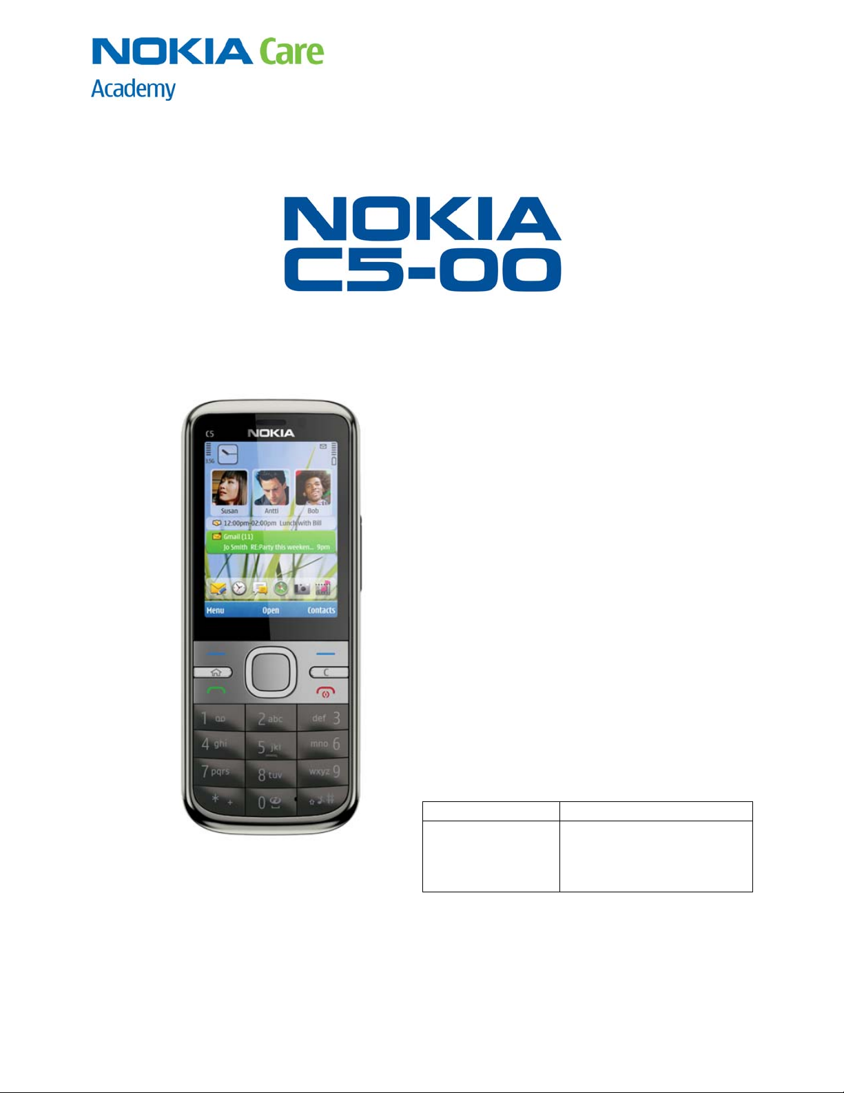
Nokia C5-00
RM-645
Transceiver characteristics
Band:
HSDPA/HSUPA, WCDMA 900/2100 + GSM/EDGE
850/900/1800/1900
Display:
QVGA (240 x 320 pixels) 2.2” screen up to 16.7 M
colors
Camera:
3.2 Mpix with Full Focus EDOF module
Operating System:
Symbian ver. 9.3
Connections:
Bluetooth wireless technology 2.1 interface
3.5 mm AV connector
Micro A/B USB 2.0 high speed
USB Charger
GPS, Maps 3.0 with Lifecaster
Transceiver with BL-5CT battery pack
Talk time Standby
GSM:
12 hours
WCDMA:
4.9 hours
GSM:
630 hours
WCDMA:
670 hours
Note: Talk times are dependant on network
parameter settings.
1
Confidential
Copyright © 2010 NOKIA All rights reserved
Version 1.0 ISSUE 1
Page 2

Nokia C5-00
RM-645
Service Manual Level 1&2
Table of Contents
Change history ......................................................................................................................................................................................... 3
1. Copyright .......................................................................................................................................................................................... 4
2. Warnings and cautions ............................................................................................................................................................... 5
2.1 Warnings ................................................................................................................................................................................ 5
2.2 Cautions .................................................................................................................................................................................. 5
3. ESD protection ................................................................................................................................................................................ 6
4. Care and maintenance ................................................................................................................................................................ 7
5. Battery information ..................................................................................................................................................................... 8
6. Exploded view ................................................................................................................................................................................ 9
7. Service devices .............................................................................................................................................................................10
8. SW-update .....................................................................................................................................................................................11
9. Disassembly instructions .........................................................................................................................................................12
10.Assembly Hints .............................................................................................................................................................................18
11.Solder Components ....................................................................................................................................................................19
2
Confidential
Copyright © 2010 NOKIA All rights reserved
Version 1.0 ISSUE 1
Page 3

Service Manual Level 1&2
CHANGE HISTORY
Status Version No. Date Comments
Approved 1.0 5.3.2010
The purpose of this document is to help NOKIA service levels 1 and 2 workshop technicians to
carry out service to NOKIA products. This Service Manual is to be used only by authorized NOKIA
service suppliers, and the content of it is confidential. Please note that NOKIA provides also other
guidance documents (e.g. Service Bulletins) for service suppliers, follow these regularly and
comply with the given instructions.
While every endeavor has been made to ensure the accuracy of this document, some errors may
exist. If you find any errors or if you have further suggestions, please notify NOKIA using the
address below:
Nokia Care Academy
mailto:Service.Manuals@nokia.com
Please keep in mind also that this documentation is continuously being updated and modified,
so watch always out for the newest version.
Nokia C5-00
RM-645
3
Confidential
Copyright © 2010 NOKIA All rights reserved
Version 1.0 ISSUE 1
Page 4

1. COPYRIGHT
Copyright © 2010 Nokia. All rights reserved.
Reproduction, transfer, distribution or storage of part or all of the contents in this document in
any form without the prior written permission of Nokia is prohibited.
Nokia, Nokia Connecting People, and Nokia X and Y are trademarks or registered trademarks of
Nokia Corporation. Other product and company names mentioned herein may be trademarks or
tradenames of their respective owners.
Nokia operates a policy of continuous development. Nokia reserves the right to make changes
and improvements to any of the products described in this document without prior notice.
Under no circumstances shall Nokia be responsible for any loss of data or income or any special,
incidental, consequential or indirect damages howsoever caused.
The contents of this document are provided “as is”. Except as required by applicable law, no
warranties of any kind, either express or implied, including, but not limited to, the implied
warranties of merchantability and fitness for a particular purpose, are made in relation to the
accuracy, reliability or contents of this document. Nokia reserves the right to revise this
document or withdraw it at any time without prior notice.
The availability of particular products may vary by region.
IMPORTANT
This document is intended for use by qualified service personnel only.
Nokia C5-00
RM-645
Service Manual Level 1&2
4
Confidential
Copyright © 2010 NOKIA All rights reserved
Version 1.0 ISSUE 1
Page 5

2. WARNINGS AND CAUTIONS
Please refer to the phone’s user guide for instructions relating to operation, care and
maintenance including important safety information. Note also the following:
2.1 Warnings
1. CARE MUST BE TAKEN ON INSTALLATION IN VEHICLES FITTED WITH ELECTRONIC ENGINE
MANAGEMENT SYSTEMS AND ANTI–SKID BRAKING SYSTEMS. UNDER CERTAIN FAULT CONDITIONS,
EMITTED RF ENERGY CAN AFFECT THEIR OPERATION. IF NECESSARY, CONSULT THE VEHICLE
DEALER/MANUFACTURER TO DETERMINE THE IMMUNITY OF VEHICLE ELECTRONIC SYSTEMS TO RF
ENERGY.
2. THE HANDPORTABLE TELEPHONE MUST NOT BE OPERATED IN AREAS LIKELY TO CONTAIN
POTENTIALLY EXPLOSIVE ATMOSPHERES, EG PETROL STATIONS (SERVICE STATIONS), BLASTING
AREAS ETC.
3. OPERATION OF ANY RADIO TRANSMITTING EQUIPMENT, INCLUDING CELLULAR TELEPHONES, MAY
INTERFERE WITH THE FUNCTIONALITY OF INADEQUATELY PROTECTED MEDICAL DEVICES. CONSULT
A PHYSICIAN OR THE MANUFACTURER OF THE MEDICAL DEVICE IF YOU HAVE ANY QUESTIONS.
OTHER ELECTRONIC EQUIPMENT MAY ALSO BE SUBJECT TO INTERFERENCE.
Nokia C5-00
RM-645
Service Manual Level 1&2
2.2 Cautions
1. Servicing and alignment must be undertaken by qualified personnel only.
2. Ensure all work is carried out at an anti–static workstation and that an anti–static wrist
3. Use only approved components as specified in the parts list.
4. Ensure all components, modules screws and insulators are correctly re–fitted after servicing
5. Ensure all cables and wires are repositioned correctly
strap is worn.
and alignment.
5
Confidential
Copyright © 2010 NOKIA All rights reserved
Version 1.0 ISSUE 1
Page 6
3. ESD PROTECTION
Nokia C5-00
RM-645
Service Manual Level 1&2
Nokia requires that service points have sufficient ESD protection (against static
electricity) when servicing the phone.
Any product of which the covers are removed must be handled with ESD
protection. The SIM card can be replaced without ESD protection if the product
is otherwise ready for use.
To replace the covers ESD protection must be applied.
All electronic parts of the product are susceptible to ESD. Resistors, too, can be
damaged by static electricity discharge.
All ESD sensitive parts must be packed in metallized protective bags during
shipping and handling outside any ESD Protected Area (EPA).
Every repair action involving opening the product or handling the product
components must be done under ESD protection.
ESD protected spare part packages MUST NOT be opened/closed out of an ESD
Protected Area.
For more information and local requirements about ESD protection and ESD
Protected Area, contact your local Nokia After Market Services representative.
6
Confidential
Copyright © 2010 NOKIA All rights reserved
Version 1.0 ISSUE 1
Page 7

4. CARE AND MAINTENANCE
This product is of superior design and craftsmanship and should be treated with care. The
suggestions below will help you to fulfil any warranty obligations and to enjoy this product for
many years.
Keep the phone and all its parts and accessories out of the reach of small children.
Keep the phone dry. Precipitation, humidity and all types of liquids or moisture can
contain minerals that will corrode electronic circuits.
Do not use or store the phone in dusty, dirty areas. Its moving parts can be
damaged.
Do not store the phone in hot areas. High temperatures can shorten the life of
electronic devices, damage batteries, and warp or melt certain plastics.
Do not store the phone in cold areas. When it warms up (to its normal temperature),
moisture can form inside, which may damage electronic circuit boards.
Nokia C5-00
RM-645
Service Manual Level 1&2
Do not drop, knock or shake the phone. Rough handling can break internal circuit
boards.
Do not use harsh chemicals, cleaning solvents, or strong detergents to clean the
phone.
Do not paint the phone. Paint can clog the moving parts and prevent proper
operation.
Use only the supplied or an approved replacement antenna. Unauthorised antennas,
modifications or attachments could damage the phone and may violate regulations
governing radio devices.
All of the above suggestions apply equally to the product, battery, charger or any accessory.
7
Confidential
Copyright © 2010 NOKIA All rights reserved
Version 1.0 ISSUE 1
Page 8

5. BATTERY INFORMATION
Note: A new battery’s full performance is achieved only after two or three complete charge and
discharge cycles! The battery can be charged and discharged hundreds of times but it will
eventually wear out.
When the operating time (talk-time and standby time) is noticeably shorter than normal, it is
time to buy a new battery. Use only batteries approved by the phone manufacturer and
recharge the battery only with the chargers approved by the manufacturer.
Unplug the charger when not in use. Do not leave the battery connected to a charger for longer
than a week, since overcharging may shorten its lifetime.
If left unused a fully charged battery will discharge itself over time Temperature extremes can
affect the ability of your battery to charge.
For good operation times with Ni-Cd/NiMh batteries, discharge the battery from time to time by
leaving the product switched on until it turns itself off (or by using the battery discharge facility
of any approved accessory available for the product).
Do not attempt to discharge the battery by any other means Use the battery only for its
intended purpose.
Never use any charger or battery which is damaged.
Do not short-circuit the battery. Accidental short-circuiting can occur when a metallic object
(coin, clip or pen) causes direct connection of the + and - terminals of the battery (metal strips
on the battery) for example when you carry a spare battery in your pocket or purse.
Shortcircuiting the terminals may damage the battery or the connecting object.
Leaving the battery in hot or cold places, such as in a closed car in summer or winter conditions,
will reduce the capacity and lifetime of the battery. Always try to keep the battery between 15°C
and 25°C (59°F and 77°F).
A phone with a hot or cold battery may temporarily not work, even when the battery is fully
charged. Batteries’ performance is particularly limited in temperatures well below freezing.
Do not dispose batteries in a fire! Dispose of batteries according to local regulations (e.g.
recycling).
Do not dispose as household waste.
Nokia C5-00
RM-645
Service Manual Level 1&2
8
Confidential
Copyright © 2010 NOKIA All rights reserved
Version 1.0 ISSUE 1
Page 9
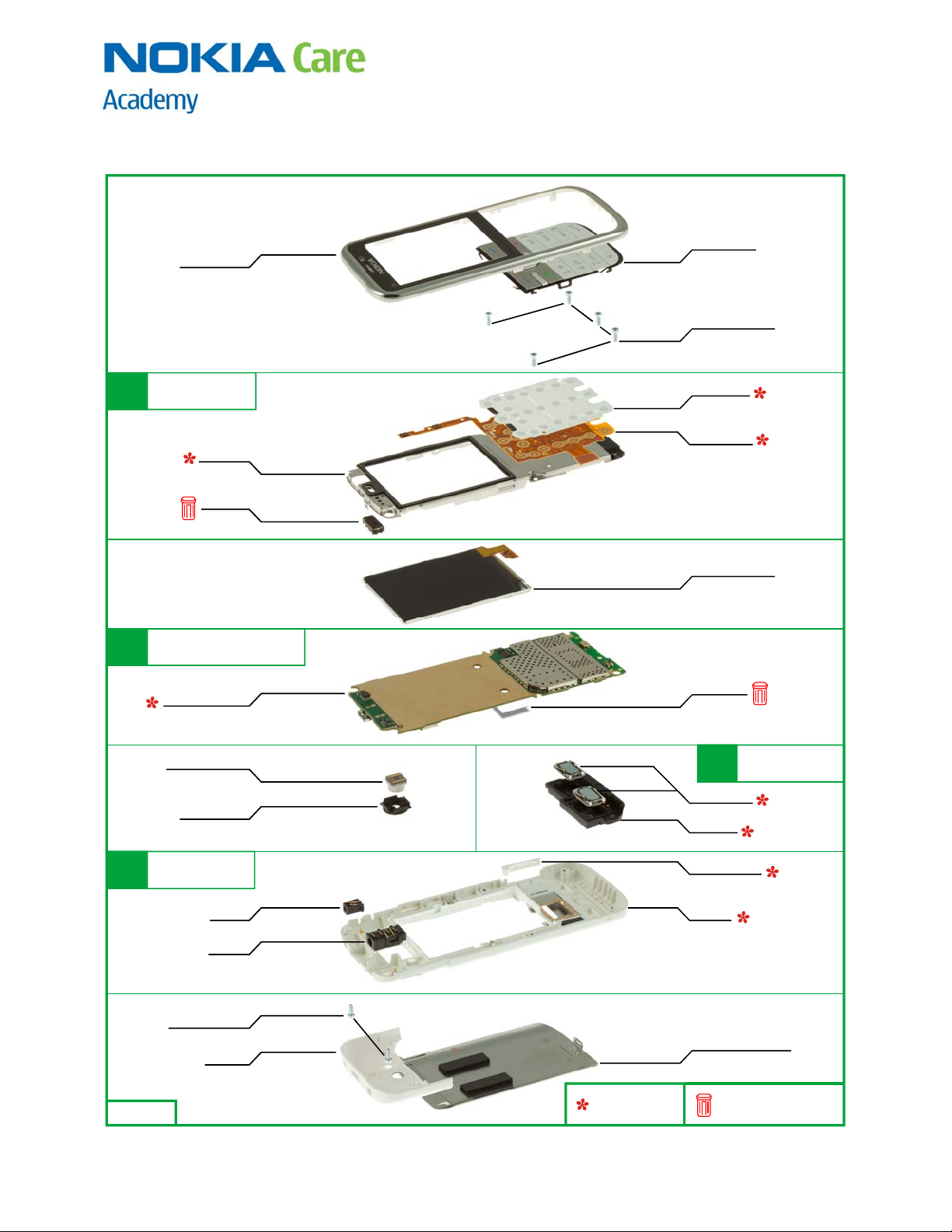
6. EXPLODED VIEW
A-COVER ASSY
I0001
Nokia C5-00
RM-645
Service Manual Level 1&2
KEYMAT ASSY
I0002
SCREWS 1.6 X 4.5
I0003
UI SHIELD ASSY
A1
(I0004 - I0007)
LIGHT SWAP PACKAGE
A2
(I0009 - I0010)
LIGHT SWAP PWB
CAMERA MODULE
CAMERA BOOT
B-COVER ASSY
A4
(I0015 - I0018)
UI SHIELD
I0006
EARPIECE
I0007
I0009
I0011
I0012
DOMESHEET
I0004
UI FLEX ASSY
I0005
DISPLAY MODULE
I0008
TYPE LABEL
I00010
ANTENNA ASSY
A3
(I0013 - I0014)
IHF SPEAKER
I0013
ANTENNA
I0014
SD CARD DOOR
I0015
DC JACK
I0016
AV JACK
I0017
SCREW 1.6 X 4.5
Ver. 1.0
9
I0019
D-COVER
I0020
Confidential
Only available as
assembly
Copyright © 2010 NOKIA All rights reserved
B-COVER
I0018
BATTERY COVER ASSY
I0021
These parts can not be
reused after removal
Version 1.0 ISSUE 1
Page 10

7. SERVICE DEVICES
Nokia C5-00
RM-645
Service Manual Level 1&2
FLS-5 Flash Device
CA-101 Service Cable
AC-3 Travel Charger
SS-88 Camera removal tool
BL-5J Battery
NMP standard toolkit (v2)
For more information, refer to the
Service Bulletin (SB-011) on NOKIA
Online. Supplier or manufacturer
contacts for tool re-order can be
found in “Recommended service
equipment” document on NOKIA
Online.
10
Confidential
Copyright © 2010 NOKIA All rights reserved
Version 1.0 ISSUE 1
Page 11

8. SW-UPDATE
Flash concept - (Point of Sales)
To use the FLS-5 Flash Dongle, follow the user guide inside the sales package.
Please check always for the latest version of flash software, wich is available on Nokia Online.
Nokia C5-00
RM-645
Service Manual Level 1&2
11
Confidential
Copyright © 2010 NOKIA All rights reserved
Version 1.0 ISSUE 1
Page 12

Nokia C5-00
RM-645
Service Manual Level 1&2
9. DISASSEMBLY INSTRUCTIONS
1) Nokia C5-00 disassembly. 2) You must use the Nokia Standard Toolkit version
2. You will also need SS-88 camera removal tool, an
AV plug and a DC plug.
3) Use the BATTERY COVER RELEASE BUTTON to open
the BATTERY COVER.
4) Place the SS-93 between the B-Cover and D-COVER
on the shown places to release the D-COVER off the
latch. Rotate the D-COVER up from the opened side.
Please note that the SS-93 tool is misplaced in the
picture. The picture will be updated in next release.
5) Remove the D-COVER. 6) Unscrew the two TORX+ size 6 screws in the order
shown.
12
Confidential
Copyright © 2010 NOKIA All rights reserved
Version 1.0 ISSUE 1
Page 13

Nokia C5-00
RM-645
Service Manual Level 1&2
7) Detach the clips holding the A-COVER ASSY by
sliding the SRT-6 in the direction shown. Do not
lever out the A-COVER as it might damage the clips
8) Continue to slide the SRT-6 along all four sides of
the device to release the remaining clips. Do not
lever out the A-COVER as it might damage the clips
9) Remove the A-COVER ASSY. 10) Protect the LCD with a protective film.
11) Press out the KEYMAT ASSY from the A-COVER
12) Remove the KEYMAT ASSY.
ASSY.
13
Confidential
Copyright © 2010 NOKIA All rights reserved
Version 1.0 ISSUE 1
Page 14

Nokia C5-00
RM-645
Service Manual Level 1&2
13) Unscrew the four TORX+ size 6 screws in the
order shown.
15) Open the second shown clip of the B-COVER
ASSY.
14) To release the engine board, open the first
shown clip holding the B-COVER ASSY with the SS-93.
16) Lift up the PWB together with UI SHIELD, LCD
and ANTENNA.
17) Remove the ANTENNA. 18) Use the SS-93 to open the UI CONNECTOR.
Be careful not to damage the connector or the
components nearby!
14
Confidential
Copyright © 2010 NOKIA All rights reserved
Version 1.0 ISSUE 1
Page 15

Nokia C5-00
RM-645
Service Manual Level 1&2
19) Remove the UI SHIELD ASSY.
20) Use the SS-93 to open the LCD CONNECTOR.
Be careful not to damage the connector!
21) Remove the LCD. 22) Use the tweezers to remove the CAMERA BOOT.
23) Use the camera removal tool SS-88, to detach
24) Lift up the SS-88 and remove the CAMERA.
the CAMERA.
15
Confidential
Copyright © 2010 NOKIA All rights reserved
Version 1.0 ISSUE 1
Page 16

Nokia C5-00
Service Manual Level 1&2
25) Use a DC plug to lift up and remove the DC JACK. 26) Use an AV plug to lift up and remove the AV
JACK.
RM-645
27) Remove the SD CARD DOOR. 28) Use the dental tool to lift up the EARPIECE.
Be aware of the sharp point of the dental tool – be
careful not to injure yourself!
29) Remove the EARPIECE using tweezers. Do not
use it again.
30) Use the dental tool to lift up one corner of the
DOMESHEET ASSY. Peel off and remove the
DOMESHEET ASSY. Do not use it again.
16
Confidential
Copyright © 2010 NOKIA All rights reserved
Version 1.0 ISSUE 1
Page 17

Nokia C5-00
RM-645
Service Manual Level 1&2
31) Use the SS-93 to release the UI FLEX ASSY from
the UI SHIELD.
32) Continue to release the UI FLEX ASSY in the
direction shown.
33) Remove the UI FLEX ASSY. Do not use it again. 34) Nokia C5-00 disassembly is now complete.
-END OF DISASSEMBLY-
17
Confidential
Copyright © 2010 NOKIA All rights reserved
Version 1.0 ISSUE 1
Page 18
Nokia C5-00
RM-645
Service Manual Level 1&2
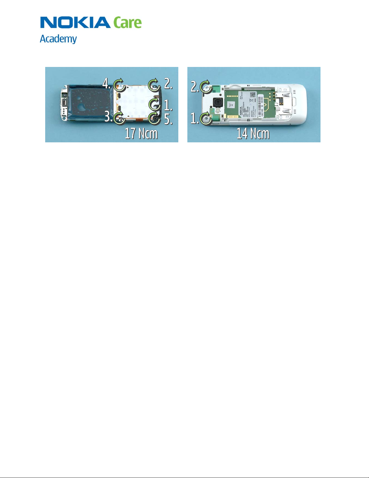
10. ASSEMBLY HINTS
1) Tighten the screw to the torque of 17 Ncm. 2) Tighten the two screws to the torque of 14 Ncm
in the order shown.
18
Confidential
Copyright © 2010 NOKIA All rights reserved
Version 1.0 ISSUE 1
Page 19

11. SOLDER COMPONENTS
Nokia C5-00
RM-645
Service Manual Level 1&2
TOP
F3300
X2450
BOTTOM
Ver. 1.0
19
F2000
Confidential
Copyright © 2010 NOKIA All rights reserved
G2200X4400
Version 1.0 ISSUE 1
Page 20

Academy
IMPORTANT
This document is intended for use by authorized Nokia
service centers only. Please use the document together
with other documents such as the Service Manual and
Service Bulletins.
Service Schematics
Version information
While every effort has been made to ensure that the document is
accurate, some errors may exist. Please always check for the latest
published version for this document.
If you find any errors in the document please send email to:
service.manuals@nokia.com
Version history
1.0 First approved version
RM-645
Table of Contents
Front page
RAPS, HS USB, Memory, Camera
GAZOO, Audio, Battery, MMC, SIM
UI, Keyboard Flex
BTH FM, GPS 5
RF Part 6
Component Finder Top 7
Component Finder Bottom 8
Component Finder Keyboard Flex 9
1
2
3
4
This material,including documentation and any related computer programs
is protected by copyright, controlled by Nokia. All rights are reserved. Copying, including reproducing, modifying, storing, adapting or translating any or
all of this material requires the prior written consent of Nokia. This material
also contains company confidential information, which may not be disclosed
to others without the prior written consent of Nokia.
Confidential Copyright © 2010 Nokia Only for training and service purposes
Page 1 (9) | Front Page | C5 RM-645 | Board: 3ft_06a | v1.0 | 03.03.2010
Page 21

Academy
CBUS(3:0)
RFCONV(20:0)
TXC(2:0)
INT_SIM(5:0)
EMINT(3:0)
DIG_AUDIO(8:0)
ACI(7:0)
INT_MMC(13:0)
LCD(99:0)
BT(23:0)
KEYB(15:0)
RFCLK(1:0)
MMC(15:0)
0
1
2
2
3
8
1
0
6
7
5
4
9
1
2
0
1
2
0
0
1 EarDataL
2 EarDataR
3 mic_data
0 audclk0
4 PMARP
5 PMARN
1
10
2
0
4
6
8
1
3
5
11
16
7
6
5
4
3
2
1
0
26
27
28
29 AC3
30 R2
0
1
3
4
5
6
7
9
10
11
11 COL4
10
9
8
7
3 ROW3
2 ROW2
0 ROW0
0
12
VCORE
C2825
C2825
1/100n
2/100n
VRFC
C2800
C2801
C2802
100n
GND GND
100n
100n
GND
GND
D2800
RAPUYAMA_V1.13_PR_RITSA_BGA401
Y15
27RR2806
100RR2803
47RR2808
ACIRx
ACITx
SD_MMCCmdDir
SD_MMCDaDir0
SD_MMCDaDir1
SD_MMCFbClk
LCD_TE
MESSI8
MESSI7
MESSI6
MESSI5
MESSI4
MESSI3
MESSI2
MESSI1
WRX
RDX
LCD_D/CX
LCD_CS
Lossi_RstX
BT_ResetX
BT_WakeUp
BTCTS
BTUARTIn
BTUARTOut
BTRTS
BTPCMClk
BTPCMOut
BTPCMIn
BTPCMSync
HostWakeUp
COL3
COL2
COL1
COL0
ROW1
ROW4
RFClkP G3
MMCCardDet
COMBO 32Mx32 DDR
C2826
C2823
18p
2u2
GND GNDGND GND GND GND
H13,H14,H15,J8,J9,J10,J11,J12,J15,J16,K8,L8,L16,M8,M9,M15,M16,N8,N15,P8,R8,R9,R11,R12,R13,R14,R15,R16,T8,T9,T10,T12,T15=VCORE
C2830
2u2
A4,A5,A7,A9,A10,A12,A15,A16,A17,A18,A21,AA1,AA15,AA23,AC5,AC6,AC7,AC8,AC13,AC15,B19,C12,C18,C23,D1,D8,D9,D12,D18,D23,E1,E3,
E23,F23,G10,H1,,H9H23,K1,L1,N2,N21,P1,T1,T2,U1,V23,Y23=VIO
A13,AA2,AA14,AA20,AA22,AB2,AB5,AB8,AB10,AB13,AC4,AC12,B3,B4,B5,B7,B8,B10,B12,B15,B18,B22,B23,C9,C10,C15,C16,C17,C19,C21,C22,D12,D14,D17,D21,D22,E2,E3,E5,
F1,F2,F3,F22,G1,G8,G16,H2,H7,H8,H9,H10,H11,H13,H16,H22,J1,J13,J14,K2,K9,K15,K16,K22,L2,L9,L15,M1,N16,P2,P9,P15,P16,P20,R10,T10,T11,T14,T16,U2,U23,Y12=GND
D3000
128Mx16 M3
C2824
1/100n
RFClkP
RFClkN
47RR2857
C2824
2/100n
AA16
AB17
G12
M20
M21
U21
D13
AB20
AC21
AB21
AB19
AC19
AC20
AA21
W20
AB4
AB7
AA9
AB3
AA7
AA5
D20
D19
D11
H17
G21
AA10
C14
L20
R23
T20
T22
P22
T21
R21
T170
Y19
U22
W4
R20
R22
M48
M7
L17
E22
L22
P23
W31
R11
H3
J3
H4
G4
F4
K4
J4
J2
K3
L3
A8
Y7
U3
U7
Y9
Y4
N9
P7
L7
R4
T3
U95 ROW5
Y84
G2RFClkN1
Y3
A1
J1
H7
F1
R8
CBusClk
CBusDa
CBusEn1X
TXQP
TXQN
IREF
TXIN
TXIP
RXQP
RXQN
RXIN
RXIP
VREFP
TxCDa
TxCDaCtrl
TxCClk
SIMClk1
SIMIOCtrl1
SIMIODa1
EMInt1
EarDataL
EarDataR
MicData
AudioClk0
PMARP
PMARN
GenIO31
GenIO32
MMCClk
MMCDa0
MMCCmd
MMCDa1
MMCDa2
MMCDa3
GenIO70
GenIO69
GenIO11
GenIO71
DISPC_DATA_LCD16
DISPC_DATA_LCD7
DISPC_DATA_LCD6
DISPC_DATA_LCD5
DISPC_DATA_LCD4
DISPC_DATA_LCD3
DISPC_DATA_LCD2
DISPC_DATA_LCD1
DISPC_DATA_LCD0
DISPC_PCLK
DISPC_HSYNC
DISPC_VSYNC
DISPC_ACBIAS
GenIO9
GenIO54
GenIO53
GenIO47
GenIO49
GenIO50
GenIO48
GenIO82
GenIO84
GenIO85
GenIO83
GenIO20
GenIO62
GenIO58
GenIO59
GenIO60
GenIO61
GenIO24
GenIO35
GenIO26
DISPC_DATA_LCD15
DISPC_DATA_LCD13
DISPC_DATA_LCD14
RFClkP
RFClkN
GenIO25
Memory
VDD
VDDATX
VDDARX
VDDA_ACS
VDDSRAMOUT
Genio28
Genio27
CCPStrbN1
CCPStrbP1
CCPDaN1
CCPDaP1
CCPStrbN0
CCPStrbP0
CCPDaN0
CCPDaP0
GenIO43
GenIO17
GenIO16
GenIO18
GenIO19
GenIO86
GenIO87
SMPSClk
SysClk384
PURX
ExtSysClkReq
SleepClk
SleepX
GenIO29
GenIO30
GenIO51
GenIO21
RFBusEn1X
TXReset
RFBusClk
RFBusDa
VDDA
SysClk192
GenIO39
GenIO72
ULPIClock
ULPIDir
ULPINxt
ULPIStp
ULPIData0
ULPIData1
ULPIData2
ULPIData3
ULPIData4
ULPIData5
ULPIData6
ULPIData7
GENIO52
GENIO04
GenIO37
I2C2SDA
I2C2SCL
GenIO23
D16
D15
Y14
Y13 1CCP1_SP
AB15 2CCP1_DN
AB14 3CCP1_DP
U13
U14 5CCP0_SP
AA14 6CCP0_DN
AA12 7CCP0_DP
U12
T7
R1
R7
AA4 20
U11
T13
E21
B6
N20
D10
D7
P21
G13
C13
G11
AC9
C7
TXA
C1
TXP
N3
A3
A20
RX1
A3
RX2
P4
N4
B3
AC16
V20
AC10
K20
K21
H21
G20
J21
J20
M22
H20
L21
F21
F20
E20
G23
B13
V21
U15
U16
Y5
VIO
R2852
R2853
3k3
3k3
FCClkN
FCClkP
FCDataN
FCDataP
MCClkN
J1402
MCDataN
MCDataP
LedFlashStrobe
FlsStrobe
FCSD
Cam2_ShutDownX
MCSD
Cam_ShutDownX
Cam_Reg_1V8
VIO
VIO
C2818
1/100n
C2820
1/100n
R2804
3k3
R2850
3k3
Cam_Reg_2V8
C2818
2/100n
C2820
2/100n
I2C2SDA
R2854
47R
R2855
47R
R2802 47R 5
R2851
3k3
47R R2856 DigiMICClk
R2805
3k3
I2C0SCL
I2C0SDA
CCP1_SN
GPSBlanking
13
12
0
4CCP0_SN
8
10
11
19
14Cam0Clk
15Cam1Clk
PURX
PURX
SleepCLK
SleepX
SleepClk
I2C1SDA
GPSResetX
C2806
1/100n
GND
C2821
1/100n
GNDGND
DigiMIC_Data
6
0
4 4 2
BT_Clk_Req
11
SleepClk
3
7
3
4I2C1SCL
1
5
2TimeStamp
6A_GPS_CLK_REQ
5
4
8
0
1
0
6
7
C2806
C2816
2/100n
1/100n
GND
C2821
C2814
2/100n
1/100n
GNDGND GND
GND
J2101
8
9
10
11
0
1
2
3
4
5
6
7
12
16
I2C2SDA
1
I2C2SCL
0
1
1
0I2C2SCL
I2C2SDA
0 I2C2SCL
PUSL(15:0)
21
GPS(15:0)
RFCTRL(11:0)
C2816
C2810
2/100n
1/100n
GND
C2841
C2814
1/100n
2/100n
1AVPAEn
4
5
2
1
0FMIRQ
D3
D2
C2
B1
A3
D3300
N3301
SCL/EN1
SDA/EN2
STROBE
SW
VIN
C1410
100n
CHRG_DET
REG1V8
RREF
VBUS
REG3V3
VBUS
VBUS
VREF
PMID
PMID
PMID
DP
DM
ID
N1400
B2=GND
C3=VIO
GND
GND
A1
A2
E3
B1
B2
B3
LED_OUT
PGND
SGND
VOUT
C1458
100n
C1454
1u
GND
D1
C1
F2
E6
C2
F4
D3
E3
C3306
100n
V3301
F3300
2.0A
L1402
L1403
X1402
X1401
GND
J3300
GND
C1408
2u2
DP_Dirty
DM_dirty
Vbus
GND
X3300
C1455
220n
GND
5
4
3
2
1
N3300
A2
A1
B1
120R/100MHz
C1453
1u
GND
C1404
1u
GND
GND
C3301
4u7
GND
K
A
GND
L7597
120R/100MHz
120R/100MHz
D1
V1413
GND
C1451
100n
C1407
2u2
C1406
10u-20u
R3300
R3302
not_assembled
STBY
VIN
12k
1k0
C3304
4u7
GND
C3312
4u7
GND
Z3301
GND
X1400
1
2
3
4
5
6
7
8
9
10
11
12
GND
N1401
GND
GND
5
A1
A2
C1
C1450
100n
GND
GND
GNDGND
GND
C3303
100n
GND
C3367
2u2
GND
C3322
4u7
GND
VCAP
VCAM_2V8
VCAM_1V8
GND
VOUT
Z3300
B2
GND
SLOWAD(6:0)
GND
C3314
GND
C1413
27p
C3300
100n
GND
CCP(20:0)
I2C_SCL
13
I2C_SDA
12
Strobe
VBAT
8
L1400
120R/100MHz
11
XSHUTDOWN
14
CAMCLK
13
I2C_SCL
I2C_SDA
12
CCP_CLKN
4
CCP_CLKP
5
CCP_DATAN
6
CCP_DATAP
7
GND
BT(23:0)
2
3
1
0
15
12
13
10
FCSD
20
Cam_Reg_2V8
Cam1V8_enable
VIO
C2810
2/100n
GND
C2841
2/100n
GND
B2100
4
VDD
3
DATA
5
GND
C2811
C2811
2/100n
1/100n
GNDGNDGND
GND
C1420
4u7
GNDGND
R2801 47R
1
L/R
2
CLK
C2116
27p
GND GND GND
C2817
1/100n
GND GND
C2817
2/100n
VDigiMic
C2115
100n
C3307
100n
GNDGND GND
19
USB(20:0)
22
16
15
14
12
9
10
11
8
0
1
2
3
4
5
6
7
16
FlsStrobe
C1411
C1405
10u
100n
GND
N1450
2
DATA-
9
DATA+
4
CLK+
5
CLK-
EXTCLK
SDA
SCL
XSHUTDOWN
1,3,6,7,12,13,19,21,23.24,25,
26,27,28,29,30,31,32=GND
N1402
C2
ON
A2
VIN
B2
VIN
C1,C2=GND
VOUT
VOUT
F3
F5
B5
C3
E5
D5
D6
A4
B1
A1
A2
A3
A5
A6
B6
C6
L1401
2u2H
20
VCAP
18
NC
10
VDIG
8
VANA
J1421
A1
B1
VCC
VCC(IO)
XTAL1
CHIP_SEL_N
DIR
NXT
STP
CLOCK
DATA0
DATA1
DATA2
DATA3
DATA4
DATA5
DATA6
DATA7
B4,C5,D2,E1,E2,E4,F1=GND
B2,B3,C4=VIO
C4
STAT
AV(5:0)
B4
I2C2(1:0)
FMRADIO(20:0)
Vchar
GND
C3365
10u
R3367
CURRENT
SENSE
2 3
1
0
L3305
4
1uH
C3316
100n
GND
C3310
10n
A4
A3
C1
C2
C3
E1
E4
E2
SDA
SCL
BOOT
SW
SW
SW
CSIN
CSOUT
AUXPWR
D1,D2,D3,D4=GND
Confidential Copyright © 2010 Nokia Only for training and service purposes
Page 2 (9) |
RAPS, HS USB, Memory, Camera | C5 RM-645 | Board: 3ft_06a | v1.0 | 03.03.2010
Page 22

Academy
GND
FMRADIO(20:0)
CBUS(3:0)
TXC(2:0)
PUSL(15:0)
GAZOOIO(3:0)
TXCCONV(4:0)
EMINT(3:0)
INT_SIM(5:0)
INT_MMC(13:0)
DIG_AUDIO(8:0)
PWRONX
X3200
1
2
3
4
5
6
7
8
SW1
VSS
SW2
GND
GND
GND
X2700
C3200
18p
N2200
GAZOO_V3.5
6
7
8
9
1
0
2
1
0
2
3
1
0
5
1
1
0
0
0
1
2
0
1
2
3
4
6
8
11
10
5
3
0
1
2
4
5
MMC(15:0)
MMCDa2
MMCDa3
MMCCmd
R3200
MMCClk
47R
MMCDa
MMCDa112
MMCDet
VIO
C2296
2u2
GND
VCORE
C2231
22u
GND
Data
C6
CLK
C1
RST
C2
VSIMGND
C3C7
R2701
0R
C2700
100n
GND
3
4
0
5
BGND GND
12
GND
C2230
22u
GND
GND
R2701
0R
2u2
GND
FM_AUDIO_PR
FM_AUDIO_NR
FM_AUDIO_PL
FM_AUDIO_NL
1
C2316
2u2
C2251
27p
R2701
0R
C2703
2u2
GND
R2200
CURRENT
SENSE
2 3
C2701C2214
27p
GND
CbusData
CbusClk
CbusSelX
J2203
J2205
SleepX
SleepClk
Purx
SIMDa
SIMIOC
SDClkA
MicData
EarDataL
EarDataR
PMARP
PMARN
C3205
100n
GND GND
0
1
2
3
4
5
4
B2200
32.768kHz
L2310
1uH
L2340
1uH
R2701
0R
G3
Mic3LP
F4
Mic3LN
G4
Mic3RP
J4
Mic3RN
N8
CBusData
N7
CBusClk
P8
CBusSelX
D3
TxCData
C2
TxCClk
B2
C2280
2u2
TxCCtrl
P2
RSTX
E3
SleepX
C4
SleepClk
A4
PURX
N11
SMPSClk
P1
GenOut1
D4
TxCOut
C3
AFCOut
A3
EMInt
C12
SIMDa
B14
SIMClk
B13
SIMIOC
E15
CMDA
M14
CMDDir
G10
Data1A
D13
Data1Dir
C14
Data2A
C13
Data3A
D14
Data4A
F13
ClkFB
E13
ClkA
D12
Data2Dir
J11
Data4Dir
E14
Data3Dir
N2
MicData
N3
AudClk
N5
EarDataL
P3
EarDataR
N1
PMARP
N4
PMARN
B10
PwrOnX
F16
VMEM
G15
CMDB
G14
Data1B
H14
Data2B
J14
Data3B
J13
Data4B
K14
ClkB
B3
SenseP
E4
SenseM
C7
VRTC
A6
CrI
B6
CrO
C15
VIOCoil
C16
VIOCoil
A13
VIO
F10
VDD18
P15
VCoreCoil
P16
VCoreCoil
T13
VCore
L16
SIMDaC
L14
SIMClkC
H11
SIMRstC
K16
VSIM
Rstx
A2,A10,B4,B5,B8,C5,C11,D6,D15,D16,E2,F1,F7,F14,G11,G16,H4,J8,K7,K8,K11,
K13,L7,L9,L15,N12,P7,P13,P14,R4,R6,R14,R15,R16,T4,T11,T14,T15,T16=GND
VCharInTest
VDDAudRx1
VDDAudRx2
VDDAudRx3
USBCharDatX
VBatChacon
VCharIn1
VCharIn2
HeadDet
HookDet
MBusTx
MBusRx
MicB2
Mic2P
Mic2N
XEarL
XEarLC
XEarR
XEarRC
VBUS
VAux1
VAux2
VOut
VRCP1
VDigiMic
VBack
VDDAudTx
VAna
BTemp
VCoreDef
VCharOut1
VCharOut1
VBatUSB
VBatVMEM
VBatVibra
VBatVibra
VBatVibra
VBatVAna
VBatVAux1
VBatVAux2
VBatVDigi
VBatVSIM
LedOut
OVVLed
OWLED
SetCurrKB
VBatLED
VBatVR1
VBatVCP
VBatIHFRN
VBatIHFRP
VBatIHFLN
VBatIHFLP
VBatVCore
VBatVCore
VBatVIO
VBatVIO
VBatVIO
VBatVIO
VBatVIO
IHFSpLP
IHFSpLN
VibraP
VibraN
IHFSpRP
IHFSpRN
EarP
EarN
VRef
VRFC
T7
R9
L8
C2012
K
A
G6
D10
B12
D11
J3
G2
F3
G1
K4
K3
K2
L3
L4
G7
A7
VBg
GND
P9
H13
G13
H8
E5
VR1
C6
A11
D8
D9
VCP
N14
F2
K1
H2
M3
B7
K9
P12
C10
BSI
M13
R8
T10
P11
N10
F15
D1
A1
B1
D7
J15
H15
F8
K15
L13
M15
H10
K10
J10
D5
B9
R7
P6
T3
P5
N16
N15
B15
A14
A15
A16
B16
P4
R3
C1
D2
R5
T6
GND
GND
HeadDet
HookDet1
MbusTx
MbusRx
L2100
1 2
3
4
C2315 C2317
2u2
2u2
GND
C2268
2u2
GND
R2071
47K
GND
R2070
GNDGND
C2227
C2314
68p
1u0
GND
C2247
C2294
2u2
2u2
GND
XEARL
XEARLC
XEARR
XEARRC
GND
C2072
27p
-t
GND
G2200
2.6V
V2300
C2253
68p
0
1
4
5
2
3
1
0
B1 B2
GND GND
4
5
6
7
VBUS
C2211
10u
GND
5
Vchar
Z2070
C2071
39p
GND
0
1
2
GND
GND
C2232
10u
C2282
2u2
V2100
VDigimic
A2A1
C2269
2u2
J2072
C2249
2u2
GND
C2326
2u2
GND
H_BRIDGE(5:0)
ACI(7:0)
XAUDIO(7:0)
C2265
SLOWAD(6:0)
X2070
VBAT
1
GND
2
BSI 3
L2300
2u2H
LED(6:0)
33nC2033
B2101
1
+
3
2
-
4
not_assembled
VRFC VAUX1VAUX2VOUT
C2266 C2267
C2222
2u2
GNDGNDGND
J2070
J2071
GND GND
BGND
GND
120R/100MHzL2202
120R/100MHzL2203
120R/100MHzL2205
120R/100MHzL2206
120R/100MHzL2207
R2044 220R
33nC2034
RFPWR(5:0)
C2271
2u22u2
2u22u2
GNDGNDGNDGND
VBAT
C2070 C2071
C2245
2u2/6V3
C2228
2u2
GND
56p150u_6V3
C2252
56p
GND
C2294
2u2
GND
GND
C2213
2u2
C2229
2u2
GND
C2281
2u2/6V3
R2037
10R
MicBias A3
Mic2P
to ASIC
C2040
2u2
GND
B3
C3
B2
C2
GND
AV(5:0)
SCL5
4
SDA
AVPaEn1 D4
5
XEARLC
4
1
3
0
XEARL
7
XEARRC
6
XEARR
C2006
2u2
GND
C2004
1/1u5
C20044
2/1u5
C2030
2/1u5
C2030
1/1u5
C2005
2u2
GND
2
3
0
1
4
5
N2037
2k0
2k2
2k2
1k0
C=1n0
N2000
D2
D3
B4
B3
C4
C3
C1
A4
B2
SCL
SDA
_SD
INL-
INL+
INR-
INR+
VDD
CPVSS
A3,C2=GND
IHFSprP
IHFSprN
IHFSpLP
IHFSpLN
VIBRAP
VIBRAN
OUTL
OUTR
CPN
CPP
25
A1
A2
A3
D3
L2107
120R/100MHz
L2108
120R/100MHz
L2101
120R/100MHz
L2104
120R/100MHz
L2105
120R/100MHz
L2106
120R/100MHz
A2 ECI
Mic2pB1
C1 Mic2n
2u2C2030
A1 A2
C1 C2
C2112
1n0
C2106
1n0
C2109
27p
C2002
27p
GND GND
Z2000
R
C
C
R
GND
GND
GND
R2010
C2113
1n0
C2107
1n0
C2110
27p
Z2001
W=0.10
FMANT
F2000
2.0A
GND
V2059
GND
120R/100MHzL2001
L2002
HS_EAR_L
21
L2003
68nH
HS_EAR_R
C2008
18p
L2109
56nH
L2110
56nH
A2
V2103
L2102
68nH
L2103
68nH
A2
V2104
C2009
18p
M2100
GND
B2103
not_assembled
B2102
not_assembled
-+
M
B2
C2117
1n0
C2118
1n0
C2108
27p
4 3
GND
A1
B1 B2
GND
A1
B1 B2
GND
E9200
E9201
HS_GND
HS_MIC
HS_EAR_R
HS_EAR_L
HS_GND
PLUG_DET
1
X2000
1
2
not_assembled
1
X2001
1
2
3
4
5
6
not_assembled
Confidential Copyright © 2010 Nokia Only for training and service purposes
Page 3 (9) |
GAZOO, Audio, Battery, MMC, SIM | C5 RM-645 | Board: 3ft_06a | v1.0 | 03.03.2010
Page 23

Academy
PWRONX
LED(6:0)
GAZOOIO(3:0)
C2500
Z4405
C2
In4
B1
In3
C1
In5
D1
X4400
1
kbc_2
2
3
kbc_3
4
VBAT
R1499
10k
R1503
R1498
0
GND
1k
V1500
2
6
2
1
27p
GND
1
R1501
100R
R1505
5
R1504
R1500
100R
47R
3
V1500
4
39R
GNDGND
V2002
V2003
R1502
LEDOUT
SetCurrKB
GND
LEDOUT
SetCurrKB
Keyboard FLEX board
5
6
7
kbr_2
8
kbr_1
9
kbc_1
10
kbr_0
11
12
kbc_4
13
14
kbr_3
15
kbr_4
16
kbc_0
17
18
kbr_5
19
20
GND
GND
X2100
1
2
3
4
5
6
7
8
9
10
11
12
13
14
15
16
17
18
19
20
21
22
GND
Row2
Row1
Row0
End_PWROn
Row3
Row4
Row5
Col2
Col3
Col1
Col4
Col0
C4401
C4402
56p
GND
56p
GND
In7
D2
In6
D1
In7
A2
In1
In4
C2
B1
In3
C1
In5
A1
In2
A1,A2,A3,A4,A5,B3,
C3,D2,D3,D5=GND
Z4404
A3,B3,C3,D3=GND
B5
Out3
C5
Out4
C4
Out5
D4
Out7
A5
Out1
A4
Out2
B5
Out3
C5
Out4
C4
Out5
D5
Out6
D4
Out7
S2019
GND
COL4
ROW3
ROW4
ROW1
ROW0
COL1
COL0
COL2
COL3
11
2
2WOR
3
4
1
5
5WOR
0
8
7
9
10
KEYB(15:0)
A A’
S2100
B B’
A A’
S2101
B
B’
C2002
56p
GND GND
S2002 S2001 S2000
C2003
S2004S2005
56p
S2006
S2003
S2007
VAUX1
GND
C2455
100n
LED(6:0)
L2451
120R/100MHz
0
1
C2457
6p8
VIO
120R/100MHz
C2454
27p
GND
C2452
100n
GND
GND
L2450
C2456
6p8
GND
VLED1+
VLED1-
C2453
27p
GND
VDDI
X2450
TE
1
2
D7
3
D5
4
5
D3
6
D1
7
D/CX
8
RDX
9
VDD
NC
10
11
12
13
14
15
16
17
WRX
18
D0
19
20
D2
21
D4
D6
22
23
CSX
24
RESX
GND
GND
C2467
C2465
C2463
C2461
C2460
33p
33p
33p
33p
GND
GND
GND
GND
C2462
33p
33p
GND
GND
Confidential Copyright © 2010 Nokia Only for training and service purposes
Page 4 (9) |
UI, Keyboard Flex | C5 RM-645 | Board: 3ft_06a | v1.0 | 03.03.2010
C2464
LCD(99:0)
LCDReset
16
7
5
3
1
28
27
26
0
2
4
6
29
30
C2000
56p
GND
C2001
56p
GND
S2012
S2017
S2021
L2000
120nH
L2003
120nH
S2008 S2010
120nH
S2013
S2018
L2001
L2004
120nH
S2014
120nH
L2002
L2005
120nH
S2009
S2015
S2011
S2016
S2020
S2025
DISPCDataLCD16
DISPCDataLCD7
DISPCDataLCD5
DISPCDataLCD3
DISPCDataLCD1
DISPCVSYNC
DISPCHSYNC
R2450
10R
C2451
C2466
33p
GND
6p8
33p
GND
GND
DISPCPCLK
DISPCDataLCD0
DISPCDataLCD2
DISPCDataLCD4
DISPCDataLCD6
DISPCACBIAS
Page 24

Academy
RFION
RFIOP
FMRF_INN
FMRF_INP
N6000
XTALP
FM_CVAR
VREGFM_DAC
VREGFM_DAC
VREGFM_DAC
VDDFM
FMVCO_LP
FMVCO_LN
VDDR5V
VDDR3V
C6008
RFCLKEXT
18
47p
C6007
10
100n
57
58
59
5
R6006
19
RES
150k
GND
8
9
1
2
L6001
56nH
C6013
1u0
GND
SYSCLK
VBAT
R3395
100R
C3393
A6
E1
L3390
470nH
C6200
33p
GND
68p
X6400
Z6000
GND
GND
1
C6016
47p
2
Bal
3
Bal
C6017
47p
6
Single
5
DC_Bias
GNDGND
C6015
1n0
Z6001
C6024
22p
L6003
47nH
L6203
1nH
GND
C6216
6p8
FMANT
Z6002
L=3.185mm
Z6003
L=2.558mm
L6002
100nH
15
14
11
12
REF_CLK
VBAT2
N6200
VDD_DIG
VDD_DIG
VDD_DIG
VCC_LNA
VCC_LNA
VCC_MIX
VCC_PLL
VCC_IF
H5
G8
B7
A1
C3
E2
A3
G2
C6207
100n
C6206
100n
C6212
100n
100n
GND
GND
GND
C6209 C6202
100n
GND GND
FMRADIO(20:0)
C6005
1
I2C_SCL
I2C_SDA2
0
FM_INTX
Mic3LP
6
Mic3RP
8
7
Mic3LN
9
Mic3RN
C6022C6023
220n
220n
GND GND
120R/100MHz
C6006
1p8
GND GND
L6000
C6004
C6010
220n
C6009
220n
1u0
J6000
39
I2C_CLK
48
I2C_DA
47
FM_IRQ_N
24
AUDIOR
22
AUDIOL
34
I2S_WS
50
VDDC
51
VDDC
52
VDDC
4
VREG_BT
13
VDDRF
17
VDDPLL
21
VDDXO
16
VDDLO
23,25,26,27,31,60,61,62,63,
64,65,66,67,68,69,70,71=GND
VDDO18
VDDO18
VDDO18
VDDO33
LPOIN
I2S/PCM_IN
I2S/PCM_OUT
I2S/PCM_SYNC
I2S/PCM_CLK
CLK_REQ
UART_WAKEUP
BT_WAKEUP
UART_CTS_N
UART_RTS_N
UART_RXD
UART_TXD
RST_N
VREG_CTL
53
54
55
56
6
46
45
42
44
28
32
35
36
43
33
30
3
1u0
GND
C6012
100n
GND
BTClkReq
R6008
2M2
C6003
1u0
GND
VIO
C6204
100n
GND
SLEEPCLK
UART_CTS
UART_RTS
UART_RX
UART_TX
21 21
8
9
10
7
2
11
1
6
3
5
4
I2S/PCM_IN
I2S/PCM_OUT
I2S/PCM_SYNC
I2S/PCM_CLK
BT_CLK_REQ
UART_WAKE
BT_WAKEUP
BT_RESETX 049
GND
C6203
100n
GND
C6205
100n
GND
BT(23:0)
H1
F4
A2
G4
G4
F5
A7
F8
G5
D7
VBAT1
VBAT1
VBAT3
SLEEPXN
SLEEPXN
I2C_UART_N
VDDS
VDDS
VDDS
RTC_CLK
GPS_EN_RESET
I2C_SDA_U1RX
I2C_SCL_U1TX
IO_TIMESTAMP_DATARDY
IO_PA_EN
AGPS_CLK_REQ
VCC_TCXO
A8,B2,B3,D2,D3,D8,E3,E4,E7,
F1,F6,F7,G1,H4,H7,H8=GND
U2TX
LNA_IN
GPS_CLK
J6200
G6
GPS(15:0)
H2
E6
B6
E8
H6
H3
L6201
D1
6n8H
F2
A4
1
3
4
2
5
6
C6201
33p
GND GND
OUT +Vcc
C6211
3p3
L6200
3n9H
G6200
16.368MHz
GND
Z6200
IN OUT
1575.42MHz
GND
GND
C6210
100n
GND
GND
X6200
IN
3
4
GND
R6215
OUT
21
X6202
0R
L6202
1n2H
Confidential Copyright © 2010 Nokia Only for training and service purposes
Page 5 (9) |
BTH FM, GPS | C5 RM-645 | Board: 3ft_06a | v1.0 | 03.03.2010
Page 25

Academy
N7560
VREF
VBB_VRX
VBB_VRX1
VB_SMPS
VB_SMPS
VB_SMPS
VB_SMPS
VB_SMPS
VB_SMPS
VB_SMPS
V8_DCDC
V8_DCDC
Test_MUX2
Test_MUX1
VRX2
CB_SMPS
IND_SMPS
IND_SMPS
IND_SMPS
IND_BOOST
IND_BOOST
IND_BOOST
IND_BOOST
G2
C7503100n
J7550
GND
C7508
10n
G1
F2
G3
C7505100n
E4
F4
F3
F1
D2
B1
A8
A9
A6
A7
C2
B7
B4
D7
B8
C7
F10
G10
K2
F11
G11
B2
A10
A11
A3
A2
A5
A4
B10
C10
E11
D11
D10
E10
C3
G9
H10
L11
J7592
J7590
141
2 OUT
C7528
2u2
L7540
33nH
C7546
10n
1 IN
3
C7545
100p
GND
Z7540
GND
X7501
Z7521
869-894/
1805-1880MHz
GND
C7535
5p6
GND
R7522 0R
L7524
15nH
GND
33
29
25
4
21
31
23
18
2
7
13
L7500
ISO 6
GND
GND
R7521
39R
C7533
10n
GND
N7540
Out1
Out2
Out3
Vbat
Vbat
Vcc2_amp2
Vcc2_amp3
Vcc1_amp3
Vcc2_amp1
Vcc1_amp1
Vcc1_amp2
5,19,27=GND
RFinRFout
GND
Icntrl1
Icntrl2
Icntrl3
C7532
18p
GND
850/900MHz
In1
In2
In3
Z7523
GND
9
11
16
6
14
20
L7521
5n6H
C7529
C7530
18p
18p
GND GND GND
T7520
C7541
1n
GND GND
GND
C7542
C7531
18p
C7580
18p
GND
C7534
100p
GND
1920-1980/1850
-1910MHz
880-915MHz
C7543
1n
L7595
3n9H
GND
C7599
1p8
GND
RFPWR(5:0)
R7560
D1
C7571
100p
GND
D2
VXO
C7573
10n
GND
H3
A3
C7572
2u2
GND
F6
F7
F8
E5
E6
E7
E8
B8
A8
H2
NC
G5
C4
A6
NC
H4
A4
NC
H5
G6
G7
G8
D5
D6
D7
D8
C5
NC
C6
NC
C7
NC
C8
NC
C7574
2u2
GND
J7538
J7536
J7537
C7567
2u2
GND
C7562
10u
GND GND GND GND GND GND
VrefRF01 4
47k
1 Vcp1
VXO
3
0 0
Vbat
C7561
10n
1uH
L7560
L7502
120R/100MHz
L7561
220R/100MHz
L7501
28R/100MHz
C7560
10u
GND GND GND
C7566
C7565
10n
10n
GND
GND
C7563
10u 1n
GND GND
C7576
2u2
C7509
2u2
C7526
8p2
GND
C7512
2u2
C7577
2u2
R7520
470R
C7527
18p
GND
C7578
5p6
N7520
26
Vsw
Icont_I
Icont_h
11
Vcc3
14
Vcc2
24
Vcc1
13
TRX1
1,8,12,15,20,22,23,25,29=GND
L7575
120R/100MHz
GND
Vgain
TX_1
TRX3
TRX2
L7541
8n2H
Ant
RX1
RX2
Vpd
VC3
VC2
VC1
TX_2
Z7542
C7520
3p3
21
18
17
28
9
2
3
5
6
7
10
27
19
16
Z7541
GND
GND
C7521
18p
GND
Z7543
GND
Z7544
GND
100n C7504
100n C7506
R7921
L7525
R7924
R7923
R7922
R7506
47R
N7500
C1PI
C1NI
C2PI
C2NI
C1PQ
C1NQ
C2PQ
C2NQ
WTRP2
WTRP1
INP_900
INM_900
INP_1800
INM_1800
DAC102
RFC6
RFC2
RFC9
RFC8
RFC7
P_OUTM
P_OUTP
RFC10
G_OUTM
G_OUTP
MUX_OUT
INP_850
INM_850
INM_2150
INP_2150
INM_1900
INP_1900
W_OUTN_H
W_OUTP_H
W_OUTP_H2
W_OUTN_H2
W_OUTN_L
W_OUTM_L
DAC203
DAC202
DAC201
VBAT_BAT
A1,B5,B6,B9,B11,C1,C6,C8,C8,C11,D1,
D9,E1,E2,F8,F9,H2,H3,H4,H7,H9,J1,J7,
K7,K10,L2,L3,L4,L6,L7,L8,L10=GND
VBEXT
VDAC
VDIG
OSCIN
REFP
REFM
REFG
DAC_REF1
RXOUT_PI
RXOUT_NI
RXOUT_PQ
RXOUT_NQ
VREF_CM
TXQ_0
TXQ_180
TXI_0
TXI_180
XRESET
XENA
SDATA
MUX_IN
VBAT_VCO
VBAT_WTX
VBAT_RX
VBAT_TX
VCP
TXC
SCLK
E3
C7500
100n
GND
K1
C7513
18p
GND
G8
K6
C7507
10n
GND
H8
C9
GND
K8
J8
L9
C7511
33p
G7500
R7510
R7500
4k7
R7505
27R
C7544
2u2
GND
R7501
10R
GND
10k
VrefRF01
4
Vcp1
1
VXO
3
C7501
10n
GND
R7502
AFC
RFClkP
RFClkN
0
TXC
1
0
1
22k
C7502
10n
GND
RFPWR(5:0)
TXCCONV(4:0)
RFCLK(1:0)
RFCLKEXT
RFCONV(20:0)
DAC_REF1
K11
K4
J4
L5
K5
J3
J11
J10
H11
J9
H6
H5
J6
J5
GND
C8
H1
E9
G4
K9
C7600
18p
L7927 15nH
L7928 15nH
C7601
18p
GND
R7504
33k
GND
C7548
18p
L7925
120R/100MHz
C7549 C7510
18p
GNDGND
18p 18p
GND
GND
RXIP
RXIN
RXQP
RXQN
VREFCM
TXQP
TXQN
TXIP30
TXIN
TXresetX
RFbusEna
RFbusDat
RFbusClk
C7547
8
4
5
6
7
9
2
1
0
8
7
6
RFCTRL(11:0)
A1
FB_DCDC
IND_DCDC
IND_DCDC
XRESET
ENABLE
DATA
SCLK
B4
NC
A7
B7
E4
F2
F1
G1
C7568
10n
L7562
3u3H
C7569
0
8
7
6
10u
GND
C7575
18p
GND
L7563
120R/100MHz
C7570
2u2
GND
RFCTRL(11:0)
A2,A5,B3,B5,B6,B7,C3,D4,E1,E2,
E3,F3,F5,G3,G4,H6,H7,H8=GND
Confidential Copyright © 2010 Nokia Only for training and service purposes
Page 6 (9) |
RF Part | C5 RM-645 | Board: 3ft_06a | v1.0 | 03.03.2010
Page 26

Academy
Top
G
D
A L
C2008 U7 C2115 A3 C2231 F8 C2271 F7 C2326 F7 C2464 H2 C2817 F3 C3303 G2 C7506 B2 C7527 C7 C7544 B2 C7567 C8 C7580 C3 L2203 E7 L7502 B7 L7925 B2 R2804 H5 R2857 H4 R7521 C3 V2300 F8 Z7543 D3
A2800 G5 C2009 U7 C2116 A4 C2232 G8 C2280 F7 C2451 H3 C2465 G2 C2818 F3 C3304 G3 C7507 C2 C7528 B5 C7545 D5 C7568 C8 C7599 A7 L2001 U7 L2204 F8 L7521 C3 L7927 B2 R1500 E8 R2805 H5 R3300 F2 R7522 D3 V3301 G2 Z7544 D3
A7500 C5 C2033 T7 C2117 H8 C2245 E7 C2281 F8 C2452 I 3 C2466 H2 C2820 E4 C3306 G2 C7508 D2 C7529 D6 C7546 B4 C
B N
C2034 T7 C2118 H7 C2247 F7 C2282 F8 C2453 H3 C2467 G1 C2821 E5 C3307 F2 C7509 B7 C7530 D6 C7547 B2 C7570 C3 C7601 C2 L2003 U7 L2206 F7 L7525 C3 R2037 U7 R2807 F6 R3395 F2 R7921 C3 X2450 H2
B2100 A3 C2040 H8 C2211 H6 C2249 H8 C2285 H7 C2454 G3 C2800 F3 C2823 E6 C3314 U2 C7510 C3 C7531 D6 C7548 B2 C7571 C7 L2100 U7 L2300 E7 L7540 D5 N1450 U3 R2044 H8 R2808 G6 R7500 B3 R7922 C3 X7501 A7
B2200 G6 C2106 H7 C2213 F8 C 2 2 5 1 F6 C2
C
C2107 H7 C2214 F7 C2252 E7 C2296 E7 C2456 H3 C2802 F3 C2825 E6 C7500 B3 C7512 B4 C7533 D6 C7560 D8 C7573 C7 D3000 G4 L2104 H7 L2340 E8 L7560 D8 N2200 G7 R2061 H6 R2851 E3 R7502 D2 R7924 D3 Z2000 T7
C1450 T2 C2108 H7 C2222 H7 C2265 F7 C2314 E8 C2457 H3 C2806 F3 C2826 E5 C7501 D2 C7513 B2 C7534 D3 C7561 C8 C7574 C8 D3300 F2 L2105 H7 L2450 I3 L7561 D7 N33
C1451 U2 C2109 I7 C2227 E8 C2266 F6 C2315 G6 C2460 H2 C2810 G6 C2830 H4 C7502 D2 C7514 C2 C7535 C3 C7562 D8 C7575 B3 L2106 H7 L2451 H3 L7562 B8 N7500 C2 R2450 H3 R2853 E5 R7505 B2 T7520 D3 Z7523 D3
C1454 U2 C2110 H7 C2228 F8 C2267 H7 C2316 H7 C2461 G2 C2811 H5 C2841 E4 C7503 B2 C7520 C7 C7541 D4 C7563 D8 C7576 D7 F3300 U2 L2107 H8 L3390 F1 L7563 B3 N7520 C6 R2801 H5 R2854 H4 R7506 D4 Z7540 C5
C1458 T2 C2112 H8 C2229 H7 C2268 F6 C2317 H7 C2462 H2 C2814 H4 C3300 F3 C 7 5 0
C2002 U7 C2113 H8 C2230 E6 C2269 H8 C2319 F7 C2463 G2 C2816 G3 C3301 F3 C7505 B3 C7526 D5 C7543 B4 C7566 C8 C7578 D7 G7500 D2 L2202 H7 L7501 D8 L7595 A7 N7560 C8 R2803 I5 R2856 I 4 R7520 D6 V2100 U7 Z7542 D5
294 H7 C2455 H3 C2801 E4 C2824 E6 C3393 F2 C7511 D3 C7532 D6 C7549 D2 C7572 D8 D2800 G4 L2101 H7 L2310 F6 L7541 B5 N2037 U7 R2060 H5 R2850 H4 R7501 D2 R7923 D3
4 B2 C7521 C5 C7542 D3 C7565 C8 C7577 D6 L2108 H8 L7500 B6 L7575 D4 N7540 C4 R2802 F6 R2855 H4 R7510 D2 V20 5 9 T7 Z75 4 1 C5
7569 B8 C7600 C2 L2002 U7 L2205 G8 L7524 D3 L7928 C2 R1501 E8 R2806 H5 R3302 G2 R7560 C7
00 T2 R2071 I6 R2852 E5 R7504 C3 Z7521 C3
F
R
X
Z
T
V
Confidential Copyright © 2010 Nokia Only for training and service purposes
Page 7 (9) |
Component Finder Top | C5 RM-645 | Board: 3ft_06a | v1.0 | 03.03.2010
Page 27

Academy
Bottom
V
F
A N
C1413 S2 C2500 G9 C4401 D7 C6016 S9 C6209 Q1 G2200 C8 L2110 B4 R1504 F7 R7928 D7 X3300 U4
A2700 D5 C1453 Q5 C2700 D7 C4402 D7 C6017 S8 C6210 R1 G6200 S2 L33 0 5 R6 N1400 S3 R1505 F8 X4400 E8
A3300 R7 C1455 S6 C2701 D7 C6003 R7 C6022 Q8 C6211 R2 L6000 Q7 N1401 Q3 R2010 U3 V1500 E7 X6200 T1
A6202 R2 C2004 U5 C3100 F4 C6004 R7 C6023 R8 C621 2 Q2 J7590 A6 L6001 R7 N1402 R4 R2070 F5 V2103 B4 X6202 T2
C2005 T6 C3200 F5 C6005 Q7 C6024 S8 C6216 S8 J 7592 A7 L6002 S8 N2000 U6 R2200 E7 V2104 B5 X6400 T8
C
C1404 R4 C2006 T6 C
C1405 S3 C2007 T6 C3310 Q7 C6007 R7 C6201 R1 E1001 L1 L1400 S4 L6200 R1 N6000 R8 R2702 D7 X1400 R5 Z3300 T3
C1406 S3 C2012 U3 C3312 R7 C6008 R8 C6202 R1 E1002 L8 L1401 T3 L6201 R1 N6200 R2 R2703 D7 X1401 R3 Z3301 T3
C1407 R3 C2030 T5 C3316 R6 C6009 R8 C6203 R1 E9200 U2 L1402 Q5 L6202 T2 R3200 F4 X1402 R3 Z4404 D7
C1408 R3 C2070 E7 C33 2 2 R7 C6010 R8 C6204 R2 E9201 U3 L1403 R4 L6203 S8 R1498 F9 R3367 R6 X2060 H1 Z4405 D7
C1409 R4 C2071 E7 C33 6 5 Q6 C6012 Q8 C6
C1410 R4 C2072 F5 C3366 R6 C6013 R8 C6206 R1 F200 0 U3 L2103 B4 R1502 F8 R6008 Q 7 X2700 D5 Z6200 S1
C1411 S3 C2253 F8 C3367 Q6 C6015 S8 C6207 R2 L2109 A4 M2100 T4 R1503 E7 R6215 T2 X3200 D2
3205 F4 C6006 R7 C6200 R2 L6003 S8 N3301 R7 R2701 D7
Confidential Copyright © 2010 Nokia Only for training and service purposes
Page 8 (9) |
Component Finder Bottom | C5 RM-645 | Board: 3ft_06a | v1.0 | 03.03.2010
J
E L
R
205 Q1 L2102 C4 L7597 R3 R1499 F9 R6006 R8 X2070 F6 Z6000 S8
M
G
X Z
Page 28

Academy
C
C2000 E2
C2001 F2
C2002 G2
C2003 H2
L
L2000 E2
L2001 H2
L2002 H2
L2003 F2
L2004 F2
L2005 H2
S
S2100 K15
S2101 K13
V
V2002 E9
V2003 H9
X
X2100 A5
TopBottom
Confidential Copyright © 2010 Nokia Only for training and service purposes
Page 9 (9) |
Component Finder Keyboard Flex | C5 RM-645 | Board: 3ft_06a | v1.0 | 03.03.2010
 Loading...