

Page 1

Nokia Customer Care
RM-8/RM-47/RM-48 Series Transceivers
6 - Troubleshooting Instructions
Issue 2 03/2005 Copyright 2005 Nokia Corporation. All rights reserved.
Page 2

RM-8/RM-47/RM-48 Company confidential
6 - Troubleshooting Instructions Nokia Customer Care
[This page left intentionally blank]
Page 2 Copyright 2005 Nokia Corporation. All rights reserved. Issue 2 03/2005
Page 3

RM-8/RM-47/RM-48
Nokia Customer Care
Table of Contents
Page No
Introduction ........................................................................................................ 1
General Failures ................................................................................................. 2
Phone is dead .................................................................................................... 2
Flash programming doesn’t work ....................................................................... 3
Charging Failure ................................................................................................ 6
Phone doesn’t stay on, or phone is jammed ...................................................... 7
Display Information: “Contact Service” .............................................................. 8
Function Failures ............................................................................................. 10
Camera Failure ................................................................................................ 10
Camera viewfinder failure ................................................................................ 11
FM-radio Failure ............................................................................................... 12
Infrared Communication Failure ....................................................................... 13
SIM Failure ....................................................................................................... 14
Display Failure ................................................................................................. 15
Main display failure ........................................................................................ 16
Mini display failure ......................................................................................... 17
Main display illumination fault ........................................................................ 18
Mini display illumination fault ......................................................................... 19
USB Data Transmission Failure ....................................................................... 20
Audio Failure .................................................................................................... 21
Uplink or downlink failure ............................................................................... 21
Uplink missing audio signal............................................................................ 22
Uplink weak audio signal ............................................................................... 23
Uplink distorted audio signal .......................................................................... 24
Uplink TDMA noise ........................................................................................ 25
Downlink missing audio signal ....................................................................... 26
Downlink weak audio signal........................................................................... 27
Downlink distorted audio signal ..................................................................... 28
Downlink noise in audio signal....................................................................... 29
Downlink TDMA noise.................................................................................... 30
Various noise problems ................................................................................. 31
Vibra errors .................................................................................................... 32
BackLight Failure ............................................................................................. 33
Key Failure ....................................................................................................... 34
Power Key Failure.......................................................................................... 34
Volume key failure ......................................................................................... 35
Keypad failure ................................................................................................ 36
RF Troubleshooting ......................................................................................... 37
RF Key Component Placement....................................................................... 38
ISSUE 2 03/2005 COMPANY CONFIDENTIAL 3
Copyright © 2005 Nokia. All Rights Reserved.
Page 4

RM-8/RM-47/RM-48
Nokia Customer Care
RF test points ................................................................................................... 39
Receiver ........................................................................................................... 40
Transmitter ....................................................................................................... 41
Synthesizer ...................................................................................................... 42
RF in General.................................................................................................... 43
RF Power Supply Configuration ..................................................................... 45
General Specifications of Transceiver........................................................... 46
Receiver Verification and Troubleshooting................................................... 48
General instructions for RX Troubleshooting ................................................... 48
Measuring RX I/Q Signals using RSSI Reading ............................................ 48
Measuring RX Performance using SNR Measurement ................................. 49
Measuring Front-End Power Levels using Spectrum Analyzer...................... 51
Measuring Analogue RX I/Q Signals using Oscilloscope .............................. 51
Fault Finding Chart of the Receiver ................................................................. 51
RX Signal Paths ............................................................................................... 56
Antenna Switch (RX/TX Switch) .................................................................... 56
RX front-end................................................................................................... 57
RX paths of RF ASIC ..................................................................................... 57
Transmitter ....................................................................................................... 58
General Instructions for Transmitter Troubleshooting ...................................... 58
Transmitter troubleshooting ............................................................................. 58
Antenna Switch (TX/RX switch) ..................................................................... 58
GSM850 Transmitter ........................................................................................ 59
General Instructions for GSM850 TX Troubleshooting .................................. 59
Fault Finding Chart for GSM850 Transmitter................................................. 62
GSM900 Transmitter ........................................................................................ 63
General Instructions for GSM TX Troubleshooting ........................................ 63
Fault Finding Chart for GSM900 Transmitter................................................. 65
GSM1800 Transmitter ...................................................................................... 68
General instructions for GSM1800 TX Troubleshooting ................................ 68
Fault finding chart for GSM1800 transmitter .................................................. 70
GSM1900 Transmitter ...................................................................................... 71
General instructions for GSM1900 TX Troubleshooting ................................ 71
Fault finding chart for GSM1900 transmitter .................................................. 73
Synthesizer ....................................................................................................... 77
Synthesizer operation check ............................................................................ 77
Reference Oscillator 26 MHz (VCTCXO) ......................................................... 79
Voltage Controlled Oscillator (VCO) ................................................................ 79
Frequencies ..................................................................................................... 81
DC Supply Current Check ............................................................................... 83
4 COMPANY CONFIDENTIAL ISSUE 2 03/2005
Copyright © 2005 Nokia. All Rights Reserved.
Page 5

RM-8/RM-47/RM-48
Nokia Customer Care
Phoenix Tuning ................................................................................................ 84
General instructions for tuning: ...................................................................... 84
RF Tuning after Repairs ................................................................................... 84
Semi-automatic Calibrations & Measurements - step by step: RX/TX and GSM-Bands
84
RX Calibration................................................................................................ 84
RX Band Filter Response Compensation ...................................................... 88
RX Channel Select Filter Calibration ............................................................. 92
TX Power Level Tuning.................................................................................. 94
TX I/Q Tuning................................................................................................. 98
Fully automatic Calibration, Tuning & Measurement by Phoenix “Auto-Tune” 104
Preparations for Phoenix ............................................................................. 104
Automatic tuning procedure ......................................................................... 107
FM-radio troubleshooting (RM-8 only) ......................................................... 109
FM-Radio Troubleshooting ............................................................................ 110
ISSUE 2 03/2005 COMPANY CONFIDENTIAL 5
Copyright © 2005 Nokia. All Rights Reserved.
Page 6

RM-8/RM-47/RM-48
Nokia Customer Care
Introduction
This document describes in overview the different hardware error possibilities for the RM-8,
RM-47 and RM-48 phone.
Not every possible hardware error is described in this document, but only those possible to correct.
Issue 2 03/2005 COMPANY CONFIDENTIAL 6
Copyright © 2005 Nokia. All Rights Reserved.
Page 7

Issue 2 03/2005
Nokia Customer Care
General Failures
■ Phone is dead
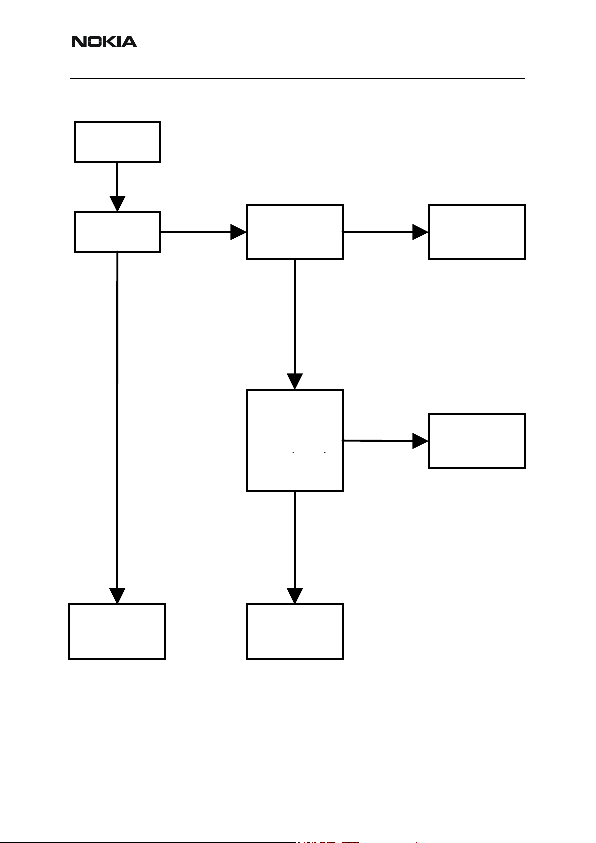
This means that the phone doesn’t use any current at all when supply is connected and/or power key is pressed. It is assumed that the voltage supplied is 3,9Vdc. UEMEK will prevent any
functionality at battery/supply levels below 2,9Vdc and the software will shut the phone down
at 3,1Vdc.
7 COMPANY CONFIDENTIAL Issue 2 03/2005
Copyright © 2005 Nokia. All Rights Reserved.
Page 8
RM-8/RM-47/RM-48
Phone is dead
Nokia Customer Care
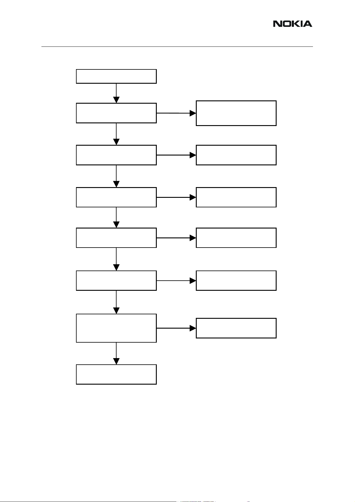
Figure 1: Phone is dead
Yes
Measure voltage on L2350, L2351,
L2352, L2353, L2354, L2355 and
L2200. Should be ~3,9V
Yes
Measure voltages on both sides of
R2407 when power key is pressed.
Should be ~0V
Yes
Sleep clock on J2800:
~32,768 kHz, 1,8Vpp
Yes
Measure voltage on PURX = 1,8Vdc
on J2802. ~1 sec after power key
is pressed.
Yes
Measure voltage on VR3=2,78 Vdc
onC2207 pin 1
No
No
No
No
No
Failure in VBATT line:
Check X2000, L2350, L2351, L2352,
L2353, L2354, L2355, L2200, C2350,
C2351, C2352 and PWB
Check:
R2407, S2401 and PWB
Check:
B2200, C2202, C2203, D2200
and PWB
Check:
D2200 and PWB
Check:
D2200, C2207 and PWB
Yes
Verify that system clock is @
~26 MHz, min 300m VACpp on
C2901 pin 2 towards D2800 (TIKU)
with regular probe C in ~10-13pF /
10M
Yes
Check:
D2800 (TIKU) and D3000 (flash)
and D3001 (SDRAM)
No
C2901, R2901, N7500 (Helgo),
Check:
G7501 (26 MHz XTAL) and PWB
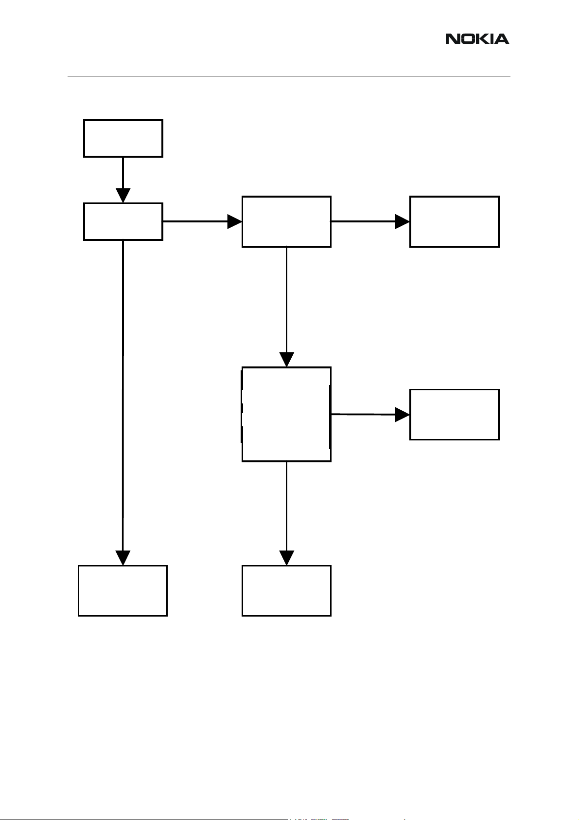
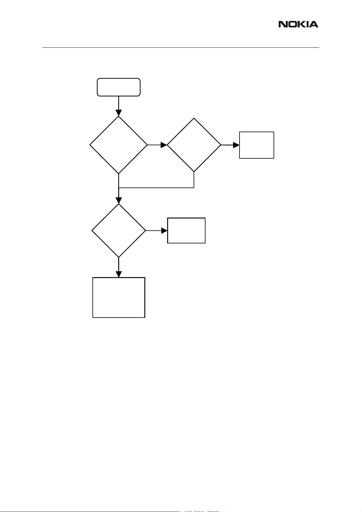
■ Flash programming doesn’t work
The flash programming on RM-8 boards is only possible via the pads on the PWB.
In case of Flash failure in production (FLALI station), problem is most likely related to SMD
problems. Possible failures could be short-circuiting of balls under µBGAs (e.g. UEMEK,
TIKUEDGE, SDRAM, FLASH), missing or misaligned components.
Issue 2 03/2005 COMPANY CONFIDENTIAL 8
Copyright © 2005 Nokia. All Rights Reserved.
Page 9
Issue 2 03/2005
Nokia Customer Care
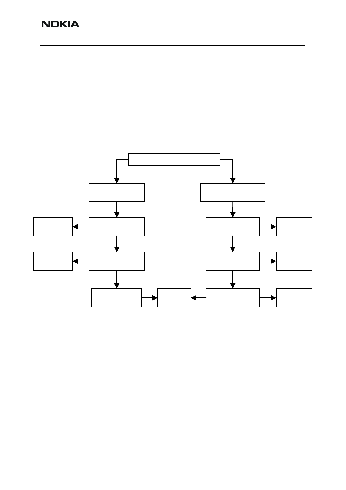
In flash programming error cases the flash prommer (via Phoenix or Darium) can give some
information about the fault. The fault information messages could be:
• Phone doesn't set Flashbus TXD line high after VCC is switch on.
• External RAM test failed.
These errors are some of the most common errors and based on this, a fault finding diagram
for flash programming is shown below. Various errors can appear from the prommer when
flashing the phone - not all of them can be directly linked to the HW or phone.
Because of the use of uBGA components, it is not possible to verify on the diagram, if there is
a short circuit in control and address/data lines on TIKUEDGE, NOR flash or SDRAM.
Figure 2: Flash programming doesn’t work
Flash programming does not work
Re-solder/Replace
component
Fix the connections
if possible. Else
scrap the phone
Prommer information is:
External RAM test failed.
(C108)
No
Check SDRAM orientation and
placement. OK?
Yes
No
Check PWB (if possible) and
power lines. Connections OK?
Yes
Replace the SDRAM Flash again
Prommer information is:
Phone does not set Flashbus TXD
line high after VCC is switched on.
Check J3401, R3400, R3403,
R3405. Connections OK?
Yes
Try reading MCU ID with
Phoenix. Reading OK?
Yes
Yes
Try reading flash ID with
Phoenix. Reading OK?
No
No
No
Re-solder/Replace
component
Replace UEMEK
or TIKU
Replace NOR
flash
9 COMPANY CONFIDENTIAL Issue 2 03/2005
Copyright © 2005 Nokia. All Rights Reserved.
Page 10
RM-8/RM-47/RM-48
Nokia Customer Care
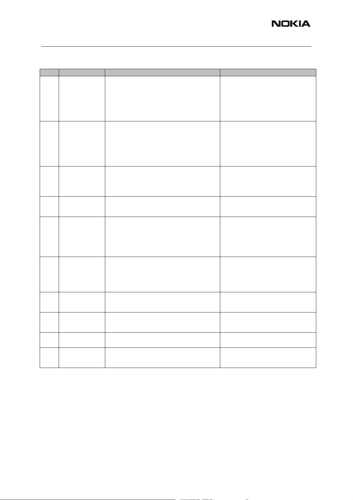
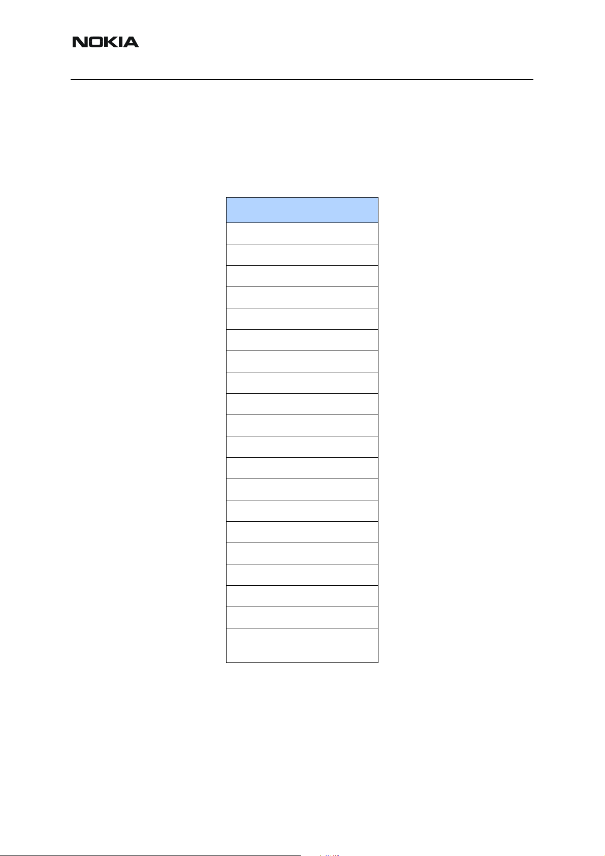
Table 1: Most common error messages
Error Description Used signals/components Points to Check
VBAT at C2228
VCORE at C2222,
VIO at C3003
VFLASH1 at R2204
FBUSRX at R3403
FBUSTX state at J2812(TIKU)-
>R3400(UEMEK)
SLEEPX at J2801
VR3 at C2227 and C7526
RFCLOCK at G7501 and R2901
MBUS pulse train at R3405
FBUSTX state at J2812(TIKU)-
>R3400(UEMEK)
MBUS pulse train at R3405
FBUSRX serial data at R3403
FBUSTX state at J2812(TIKU)-
>R3400(UEMEK)
Prommer SW
C101
C102
C103
C107
A204
A387
C583
C683
C584
C684
C585
C685
C586
C686
The Phone does not
set Flashbus TXD
line high after the
The Phone does not
set Flashbus TXD
line low after the line
has been high. The
Prommer generates
this error also when
the Phone is not
connected to the
The Phone MCU
has not received the
first dummy word
correctly from the
Prommer after the
The Phone MCU
can not start
Secondary code
manufacturer and
device IDs in the
existing Algorithm
files do not match
with the IDs
received from the
target phone.
The MCU ID in the
FIASCO_MCU_ID_I
NFO block of the
MCUSW file does
not match with the
ID received from the
target phone.
The Prommer has
not received Phone
acknowledge to the
The Phone has
generated NAK
signal during data
block transfer.
The Phone has not
acknowledged data
block correctly.
The erasing status
response from the
Phone informs about
startup.
Prommer.
startup.
correctly.
The flash
message.
fail.
VBAT, VCORE, VIO, VFLASH1
BSI and FBUSRX from Prommer to UEMEK
FBUSTX from TIKU->UEMEK->Prommer (stuck at ‘0’)
SLEEPX from UEMEK to TIKU
RFCLOCK (VCTCX->Helgo->TIKU)
MBUS From Prommer->UEMEK->TIKU(stuck at ‘1’)
FBUSTX from TIKU->UEMEK->Prommer(stuck at ‘1’)
MBUS from Prommer->UEMEK->TIKU(stuck at ‘0’)
FBUSRX from Promm er->UEMEK->TIKU
FBUSTX from TIKU->UEMEK->Prommer
Signals between TIKU and Flash
Signals between TIKU and Flash
Signals between TIKU and Flash
Signals between TIKU and Flash
PURX, VR3
TIKU
Flash
TIKU Prommer SW
Flash and TIKU
Flash and TIKU
Flash and TIKU
Flash
BSI pulse at C2003 when flashing starts
PURX state transition ‘0’ to ‘1’ at J2802
Issue 2 03/2005 COMPANY CONFIDENTIAL 10
Copyright © 2005 Nokia. All Rights Reserved.
Page 11
Nokia Customer Care
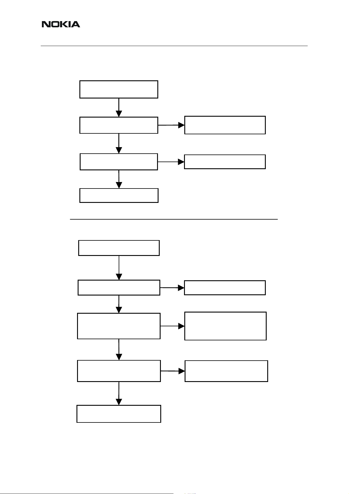
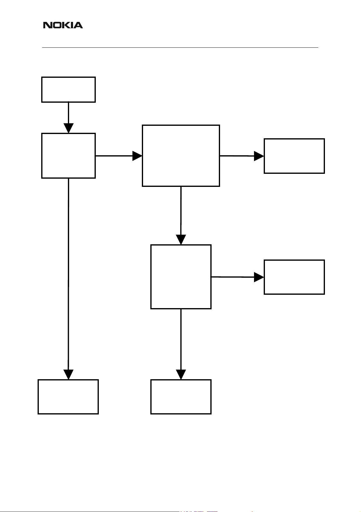
■ Charging Failure
Charging fails and no current
drawn from ‘charger’
Yes
Issue 2 03/2005
Measure Vchar voltage
on V2000. Is it > 3.0V?
Yes
Recalibrate charger circuitry
and retest. Did it work?
Yes
END
Display information when charger
connected: “Not charging”
Yes
Recalibrate charger circuitry
and retest. Did it work?
No
No
Yes
X2003, F2000, L2000, V2000,
Check:
C2005, C2006 and PWB
D2200 (UEMEK) is faulty
END
No
Verify through Phoenix that BSI=
~68k Ohm (BL-4C) and BTEMP=
~47k Ohm @ roomtemperature
(~25 C)
Yes
Measure voltage on R2200 towards
D2200. Should be the same as
Vbat voltage
Yes
Phone should work. If not,
change whole engine board
No
No
BSI: Battery (BL-4C), R2015
C2003, R2361, R2362 and PWB
BTEMP: R2000, C2004, R2360,
R2200, D2200 (UEMEK) and PWB
Check:
R2363 and PWB
Check:
11 COMPANY CONFIDENTIAL Issue 2 03/2005
Copyright © 2005 Nokia. All Rights Reserved.
Page 12
RM-8/RM-47/RM-48
Nokia Customer Care
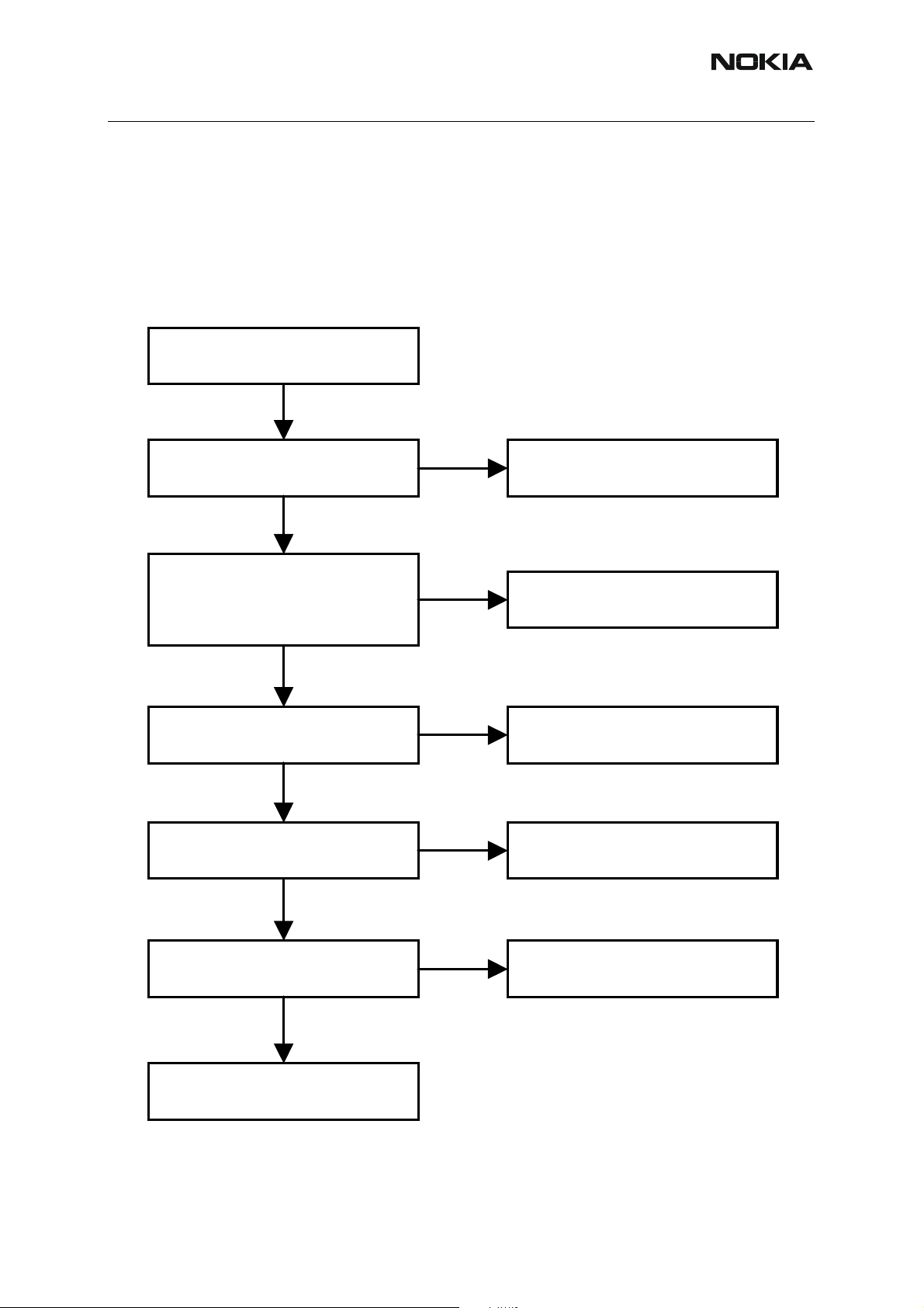
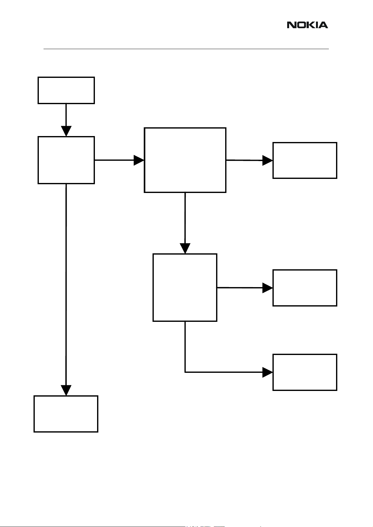
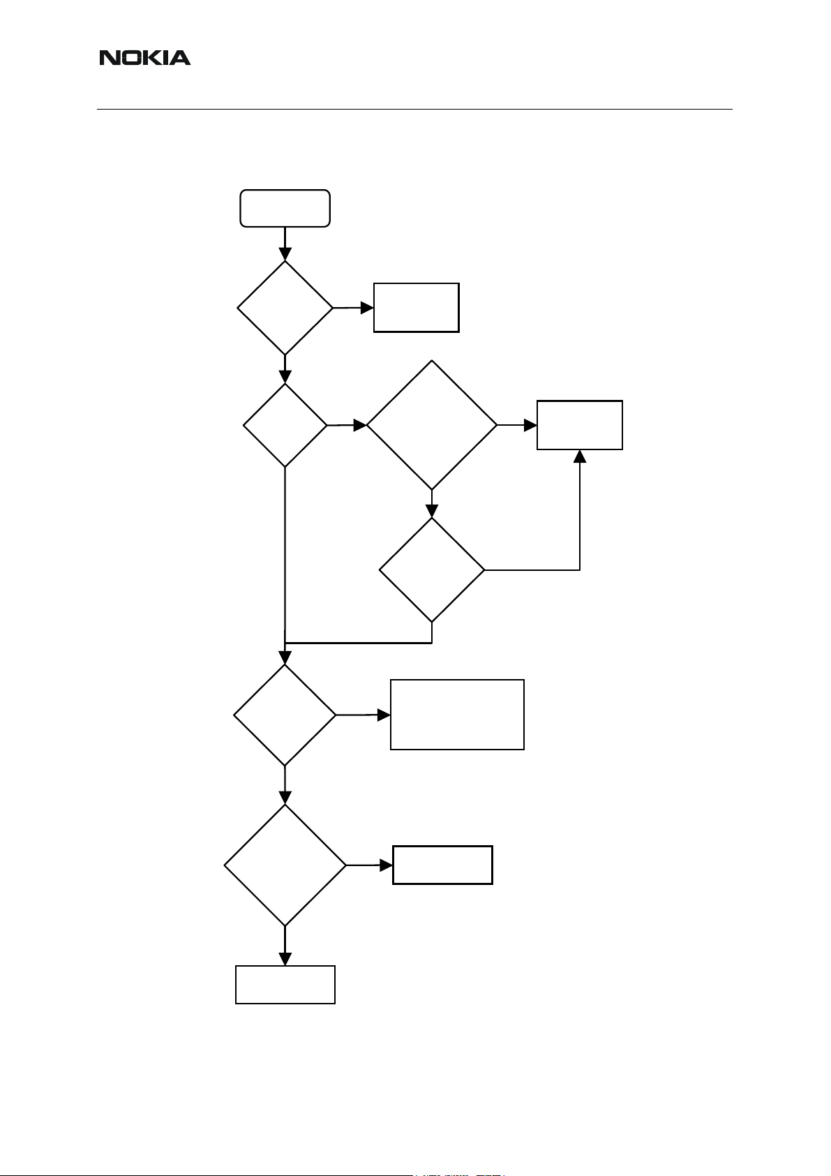
■ Phone doesn’t stay on, or phone is jammed
If this kind of a failure is presenting itself immediately after FLALI, it is most likely caused by
ASICs missing contact with PWB.
If the MCU doesn’t service the watchdog register within the UEMEK, the operations watchdog
will run out after approximately 32 seconds. It is not possible to measure this service routine.
Figure 3: Phone doesn’t stay on, or is jammed
Phone doesn’t stay on or phone is
jammed
Yes
Sleep clock on J2800
~32,768 kHz; 1,8Vpp
Yes
Verify that system clock is @
~26 MHz, min 300m VACpp on
C2901 pin2 towards D2800 (TIKU)
with regular probe Cin ~10-13pF /
10M
Yes
Measure voltage on PURX=
1,8 Vdc on J2802
~1 sec after power key is pressed
Yes
No
No
No
B2200, D2200 (UEMEK),
Check:
C2202, C2203 and PWB
Check:
C2901, R2901, N7500 (Helgo),
G7501 (26 MHz XTAL) and PWB
Check:
D2200 (UEMEK) and PWB
UI functionality and keys react to
pressure?
Yes
Is everything working until phone
shuts down after ~32 sec?
No
Retest and if phone still doesn’t work,
change whole engine board
No
D2800, D3000, D3001, Z2400, Z2401,
keymat, lightguide and PWB
Yes
Change D2200 (UEMEK)
Check:
Issue 2 03/2005 COMPANY CONFIDENTIAL 12
Copyright © 2005 Nokia. All Rights Reserved.
Page 13
Issue 2 03/2005
Nokia Customer Care
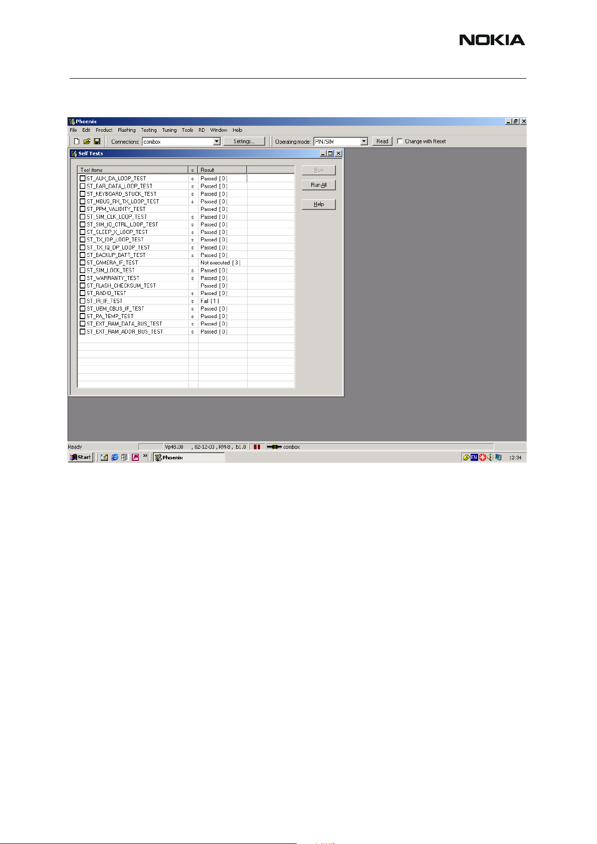
■ Display Information: “Contact Service”
When this error appears in the display it means that one or more of the internal baseband tests
has failed. The baseband tests (self tests) are performed each time the phone is powered on.
The self tests are divided into those performed while powering up (Start up tests) and the ones
that can be executed with a PC using Phoenix (Runtime tests). The following Start-up tests are
performed during power up:
AUX DA LOOP TEST
EAR DATA LOOP TEST
KEYBOARD STUCK TEST
MBUS RX TX LOOP TEST
PPM VALIDITY TEST
SIM CLK LOOP TEST
SIM IO CTRL LOOP TEST
SLEEP X LOOP TEST
TX IDP LOOP TEST
TX IQ DP LOOP TEST
BACKUP BATT TEST
CAMERA IF TEST
SIM LOCK TEST
WARRANTY TEST
FLASH CHECKSUM TEST
RADIO TEST
IR IF_TEST
UEM CBUS IF TEST
PA TEMP TEST
EXT RAM DATA BUS TEST
EXT RAM ADDR BUS
TEST
If all these self tests are passed, the phone will start up.
From Phoenix it’s possible to run all the self tests and the additional “Runtime test”. The test
cases can be seen below.
13 COMPANY CONFIDENTIAL Issue 2 03/2005
Copyright © 2005 Nokia. All Rights Reserved.
Page 14
RM-8/RM-47/RM-48
Nokia Customer Care
Figure 4:Display Information: “Contact Service”
Issue 2 03/2005 COMPANY CONFIDENTIAL 14
Copyright © 2005 Nokia. All Rights Reserved.
Page 15
Nokia Customer Care
Function Failures
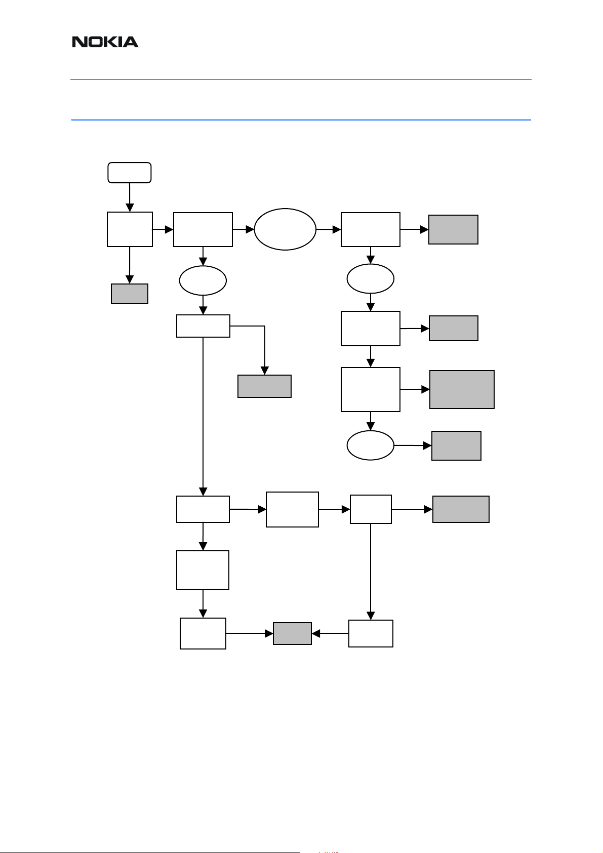
■ Camera Failure
Start
Issue 2 03/2005
Does the
viewfinder
start?
Yes
End
No
Check engine PWB
in module jig. Does
camera work?
No
Check X2400.
Failure in
Lower block
OK?
Yes
Displays
(VCORE_LIN)
working OK?
Yes
No
Change/fix
and retest
No
Failure in
Upper block OR
Hinge Flex
Check
VCORE_LIN 1.8V
from module jig.
OK?
Check Upper block
in module jig. Does
camera work?
No
Failure in
Upper block
Check Camera
positioning in
socket X3603.
Yes
Check X3602,
C3609-C3612,
Z3601,
C3624- C3625
and lines. OK?
Yes
Failure in
Camera
module
No
Check C2222
(1/2). OK?
Yes
OK?
YesYes
No
No
No
Failure in Hinge
Flex. Change
and retest.
Adjust & retest
According to repair
instructions –repair
or change Upper
block Flex As sy
Change Upper
block Flex Assy
and retest.
Change/fix
defect component
and retest
Measure
CamCtrlClk from
module jigs
test point. Is it
13 MHz?
No
Change
TIKU
(D2800)
Retest
Change UEMEK
(D2200)
15 COMPANY CONFIDENTIAL Issue 2 03/2005
Copyright © 2005 Nokia. All Rights Reserved.
Page 16
RM-8/RM-47/RM-48
■ Camera viewfinder failure
Viewfinder working but no
picture taken when pressing
select-key
Nokia Customer Care
Select key
functional ?
Yes
R3304 = 6,5 MHz
clock when
pressing select?
Yes
No
No
Check
keyboard with
Phoenix
Check for
short circuit
of R3304
Z2401 and
domesheet
OK ?
Yes
Short circuit?
Yes
No
No
Replace
Z2401 and/or
domesheet
PWB
failure
Camera
failure
Replace
component
Reflash phone
Issue 2 03/2005 COMPANY CONFIDENTIAL 16
Copyright © 2005 Nokia. All Rights Reserved.
Page 17

Nokia Customer Care
■ FM-radio Failure
The FM-radio troubleshooting guide is in the RF section.
Issue 2 03/2005
17 COMPANY CONFIDENTIAL Issue 2 03/2005
Copyright © 2005 Nokia. All Rights Reserved.
Page 18
RM-8/RM-47/RM-48
■ Infrared Communication Failure
IrDA failure
Yes
Nokia Customer Care
Measure
VBAT at C2600
= 3,7- 4,2 V?
Yes
Measure
VFLASH1 at
C2602
= 2,78 V?
Yes
Measure
VIO at
C2603
= 1,80 V?
No
No
No
Defect PWB
Replace
D2200
Replace
D2200
Yes
Measure
activity TXD
on N2600
pin3?
Yes
Replace
N2600
No
Replace
D2800
Issue 2 03/2005 COMPANY CONFIDENTIAL 18
Copyright © 2005 Nokia. All Rights Reserved.
Page 19
Issue 2 03/2005
Nokia Customer Care
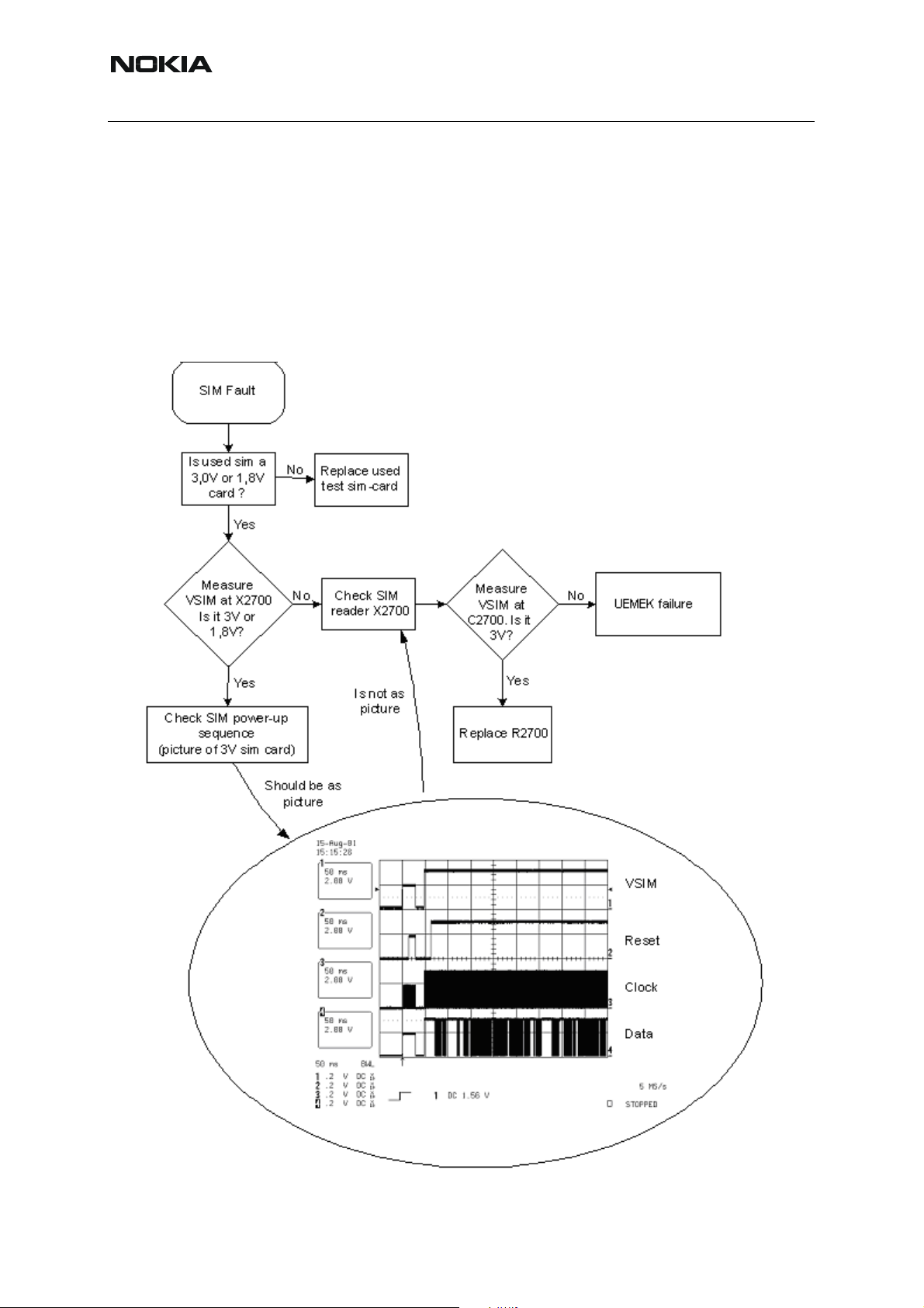
■ SIM Failure
The hardware of the SIM interface from the UEMEK (D2200) to the SIM connector (X2700) can
be tested without a SIM card. When the power is switched on, the phone first checks for a 1,8V
SIM card and then a 3V SIM card. The phone will try this four times, whereafter it will display
"Insert SIM card".
The error ”SIM card rejected” means that the ATR message received from the SIM card is corrupted, e.g. data signal levels are wrong. The first data is always ATR and it is sent from card
to phone.
Figure 5: SIM Failure
19 COMPANY CONFIDENTIAL Issue 2 03/2005
Copyright © 2005 Nokia. All Rights Reserved.
Page 20
RM-8/RM-47/RM-48
■ Display Failure
Start
Nokia Customer Care
Do
both displays
start ?
Yes
No
Both
displays
fail?
Yes
Check Hinge
flex, X2400,
X3602. OK ?
Yes
Measure VFlash1
Measure
at 1/2 of C2220
VDD (~2,8V)
and Vcore_Lin at
from C2220
1/2 of C2222.
VDDI (~1,8V)
OK?
from C2222
No
No
No
Main display
fails
Mini display
fails
Change defect
components.
OK ?
Check Hinge
flex, X2400,
X3602 and
lines. OK ?
No
No
Go to “Main display
failure”
Go to “Mini display
failure”
Change upper
block.
Change UEMEK
(D2200)
Yes
END
Measure RESX
Measure
from X2400
RESX from
(~1,8V). OK?
C2222
(~1,8V). OK ?
Yes
Are the
backlights OK ?
No
No
Check Hinge
flex, X2400,
X3602 and
lines. OK ?
No
Change TIKU
(D2800)
Go to
“Main/Mini display
illumination
fault”
Issue 2 03/2005 COMPANY CONFIDENTIAL 20
Copyright © 2005 Nokia. All Rights Reserved.
Page 21
Nokia Customer Care
Main display failure
Start
Issue 2 03/2005
Main display
fails ?
No
Yes
Check hinge flex,
X2400, X3600
and X3602. OK ?
Yes
Measure
VFlash1
VDD (~2,8V)
from C3607,
Vcore_lin (1,8V)
VDDI (~1,8V)
from C3608.
OK ?
No
No
Change defect
components.
OK ?
Change UEMEK
(D2200)
Yes
END
21 COMPANY CONFIDENTIAL Issue 2 03/2005
Copyright © 2005 Nokia. All Rights Reserved.
Change display
module
Page 22
RM-8/RM-47/RM-48
Mini display failure
Start
Nokia Customer Care
Mini display
fails ?
No
Yes
Check hinge flex,
X2400, X3601
and X3602. OK ?
Yes
Measure
VFlash1 (
VDD (~2,8V)
from C3606,
Vcore_lin (1,8V)
VDDI (~1,8V)
from C3605.
OK ?
Yes
No
No
Change defect
components.
OK ?
Change UEMEK
(D2200)
END
Issue 2 03/2005 COMPANY CONFIDENTIAL 22
Copyright © 2005 Nokia. All Rights Reserved.
Change display
module
Page 23
Nokia Customer Care
Main display illumination fault
Start
Issue 2 03/2005
Are the Main
display
backlights
OK ?
Yes
No
Check N2400, V2404,
R2403, C2411- C2413,
L2400, X2400, X3602
(Hinge flex) and
X3600. OK ?
Yes
Measure
VLED+ (~14V)
from V2404.
OK ?
No
No
Change defect
components.
Retest.
Change UEMEK
(D2200)
Yes
END
23 COMPANY CONFIDENTIAL Issue 2 03/2005
Copyright © 2005 Nokia. All Rights Reserved.
Change display
module
Page 24
RM-8/RM-47/RM-48
Mini display illumination fault
Start
Nokia Customer Care
Are the Mini
display
backlights
OK ?
Yes
No
Check D2400, R2400,
C2402, C2403,
X2400, X3602
(Hinge flex) and
X3601. OK ?
Yes
Check LED’s
V3600, V3601,
V3602 and
lines.
OK ?
No
No
Change defect
components.
Retest.
Change defect
components.
Retest.
Yes
Change UEMEK
(D2200).
END
Issue 2 03/2005 COMPANY CONFIDENTIAL 24
Copyright © 2005 Nokia. All Rights Reserved.
Page 25
Nokia Customer Care
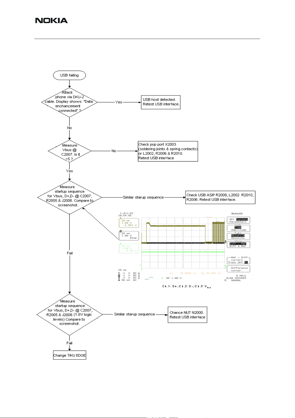
■ USB Data Transmission Failure
Issue 2 03/2005
25 COMPANY CONFIDENTIAL Issue 2 03/2005
Copyright © 2005 Nokia. All Rights Reserved.
Page 26
RM-8/RM-47/RM-48
■ Audio Failure
Uplink or downlink failure
Nokia Customer Care
Start
Uplink = outgoing
audio from e.g. microphone
Is there
an audio
signal?
Yes
Is audio
level
sufficient?
Yes
Is audio
signal
undistorted?
Yes
Is TDMA
noise
inaudible?
No
No
No
No
Uplink
Go to “Uplink
missing audio
signal”
Go to “Uplink
weak audio
signal
Go to “Uplink
distorted audio
signal”
Go to “Uplink
TDMA noise”
”
Is problem
uplink or
downlink?
Downlink = incoming
audio to e.g. earpiece
Downlink
Is there
an audio
signal?
Yes
Is audio
level
sufficient?
Yes
Is audio
signal
undistorted?
Yes
Is audio
signal free
of noise?
No
No
No
No
Go to
“Downlink
missing audio
signal”
Go to
“Downlink
weak audio
signal
”
Go to
“Downlink
distorted audio
signal”
Go to
“Downlink
audio signal
noise”
Yes
Is there no
acoustical
feedback?
Yes
No
Go to
“Acoustical
feedback”
Is TDMA
noise
inaudible?
Yes
Is there no
acoustical
feedback?
Yes
Click noise, audio
signal too loud or
bad picture/
sound
synchronization
No
No
No
Go to
“Downlink
TDMA noise ”
Go to
“Acoustical
feedback”
Software
error or bad
TIKU
Issue 2 03/2005 COMPANY CONFIDENTIAL 26
Copyright © 2005 Nokia. All Rights Reserved.
Page 27
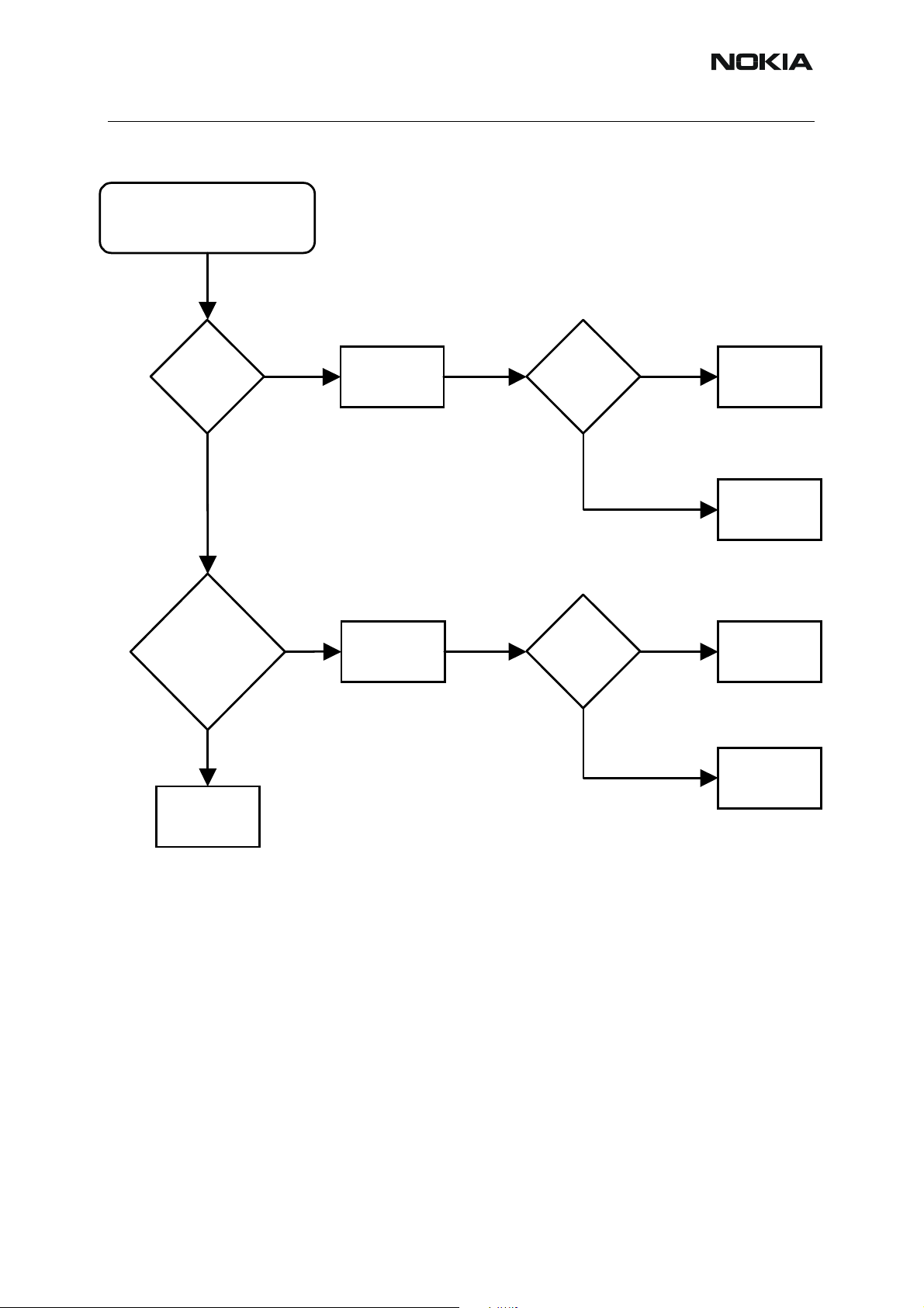
Nokia Customer Care
Uplink missing audio signal
Issue 2 03/2005
Start
Yes
Is mute
deactivated?
Yes
Is problem
present both with
hand portable
and accessory?
No
Is problem
solved when
using
accessory?
Yes
Measure
mic bias. Is it
~2.1V?
No
Deactivate mute
Yes
No
Accessory is
C2107, C2108 and R2104,
in menu
defective
Are any of
the bias components
defective? (Check R2113,
for hand portable and
R2105, C2111, C2112
and R2107 for
accessory)
Yes
NoNo
Replace
UEMEK
Are microphone
contacts and PWB
pads OK?
Yes
Are any of
the components
(L2100, C2109, R2100,
C2100 or C2101 for hand
portable and L2101, C2104
or C2103 for accessory)
missing or
damaged?
No
Replace
microphone
Yes
No
Replace
defective parts.
Is bias ~2.1V?
Yes
No
Clean contacts and pads. If
tracks are badly corroded it
may not be possible to
repair the phone
Replace
defective parts
27 COMPANY CONFIDENTIAL Issue 2 03/2005
Copyright © 2005 Nokia. All Rights Reserved.
Page 28
RM-8/RM-47/RM-48
Uplink weak audio signal
Start
Nokia Customer Care
Is
microphone
opening
clean?
Yes
Measure
bias. Is it
~2.1V?
Yes
No
No
Clean opening
Are any of the bias
components defective?
(Check R2113, C2107,
C2108 and R2104)
Yes
Replace
defective parts.
Is bias ~2.1V?
Yes
No
No
Replace
UEMEK
Are microphone
contacts and PWB
pads OK?
Yes
Are any of the
components
L2100, C2109,
R2100, C2101 or C2100
missing or
damaged?
No
Replace
microphone
No
Yes
Clean contacts and pads. If
tracks are badly corroded it
may not be possible to
repair the phone
Replace
defective parts
Issue 2 03/2005 COMPANY CONFIDENTIAL 28
Copyright © 2005 Nokia. All Rights Reserved.
Page 29
Nokia Customer Care
Uplink distorted audio signal
Start
Issue 2 03/2005
Is there
distortion when
using
accessory?
No
Measure
bias. Is it
~2.1V?
Yes
No
Yes
Defect accessory
Are any of the bias
components defective?
(Check R2113, C2107,
C2108 and R2104)
Yes
Yes
Replace
defective parts.
Is bias ~2.1V?
No
No
Replace
UEMEK
Are microphone
contacts and PWB
pads OK?
Yes
Are any of the
components
L2100,C2109, R2100,
C2100 or C2101
missing or
damaged?
No
Replace
microphone
No
Clean contacts and pads. If
tracks are badly corroded it
may not be possible to
repair the phone
Yes
Replace
defective parts
29 COMPANY CONFIDENTIAL Issue 2 03/2005
Copyright © 2005 Nokia. All Rights Reserved.
Page 30
RM-8/RM-47/RM-48
Uplink TDMA noise
Nokia Customer Care
Start
Is there TDMA
noise both in hand
portable and when
using accessory?
Yes
Replace
the microphone.
Is there still
noise?
Yes
Check for loose,
missing or damaged
shielding cans. Check
C2101, C2107 - C2109
for handportable and
C2110 - C2112 for
accessory
No
No
Is there noise
only in hand
portable mode?
Yes
Defective
microphone
No
Defective
accessory
Issue 2 03/2005 COMPANY CONFIDENTIAL 30
Copyright © 2005 Nokia. All Rights Reserved.
Page 31

Nokia Customer Care
Downlink missing audio signal
Start
Issue 2 03/2005
Is problem
present both in
hand portable mode
and when using
FM radio?
Both
Is problem
present both in
speakers
and with
accessory?
Yes
FM radio
No
Is external
antenna
(headset)
working?
Is problem
related to
earpiece, IHF or
accessory?
Yes
IHF
No
Accessory is not
detected or it is
defective
FM module is
defective
IHF is defective.
Check IHF speaker
and connections.
Check L2105, L2104,
C2114, C2116,
C2118 - C2121, N2100,
R2115 – R2117, R2119,
R2120. Check UEMEK.
Accessory
Earpiece
Accessory is
defective
Earpiece is defective.
Check earpiece speaker
and connections.
Check R2137 and
R2138. Check UEMEK.
Software or UEMEK
is defective
31 COMPANY CONFIDENTIAL Issue 2 03/2005
Copyright © 2005 Nokia. All Rights Reserved.
Page 32

RM-8/RM-47/RM-48
Downlink weak audio signal
Start
Is IHF opening
clogged?
Yes
Nokia Customer Care
Clean IHF
opening
Is problem
present both in
earpiece
and IHF?
Yes
No
Is problem
related to
earpiece or
IHF?
Earpiece
IHF
No
Is earpiece
opening
clogged?
No
IHF is defective.
Check IHF speaker
and connections.
Check L2105, L2104,
C2114, C2116,
C2118 - C2121, N2100,
R2115 – R2117, R2119,
R2120. Check UEMEK.
Yes
Clean earpiece
opening
Earpiece is defective.
Check earpiece speaker
and connections.
Check R2137 and
R2138. Check UEMEK.
Software or UEMEK
is defective
Issue 2 03/2005 COMPANY CONFIDENTIAL 32
Copyright © 2005 Nokia. All Rights Reserved.
Page 33

Nokia Customer Care
Downlink distorted audio signal
Start
Issue 2 03/2005
Is problem
present both in
earpiece and
IHF?
Yes
No
Is problem
related to earpiece
or IHF?
Earpiece
IHF
IHF is defective.
Check IHF speaker
and connections.
Check L2105, L2104,
C2114, C2116,
C2118 - C2121, N2100,
R2115 – R2117, R2119,
R2120. Check UEMEK.
Earpiece is defective.
Check earpiece speaker
and connections.
Check R2137 and R2138.
Check UEMEK
Software, FM module
or UEMEK
is defective
33 COMPANY CONFIDENTIAL Issue 2 03/2005
Copyright © 2005 Nokia. All Rights Reserved.
Page 34

RM-8/RM-47/RM-48
Downlink noise in audio signal
Start
Nokia Customer Care
Is the noise
electrical or
mechanical?
Electrical
Is the noise
associated with
earpiece/IHF
(hand portable
mode) or
FM radio?
FM radio
Is the noise
associated with
accessory?
Mechanical
Earpiece/IHF
No
Loose speaker or
other component
inside the phone
No
Does the error
occur both
in earpiece and
IHF?
Yes
Defective FM
Defective
speaker
Software error.
Defective or
badly tuned
antenna
module
Yes
Defective
accessory
Issue 2 03/2005 COMPANY CONFIDENTIAL 34
Copyright © 2005 Nokia. All Rights Reserved.
Page 35

Nokia Customer Care
Downlink TDMA noise
Start
Issue 2 03/2005
Is there TDMA
noise both in hand
portable and when
using accessory?
Yes
Replace battery.
Is there still noise?
Yes
No
No
Is there noise
only in hand
portable mode?
Yes
Defective
battery
Check for loose, missing
or damaged shielding cans.
Mistuned antenna.
Missing/bad component.
Check that the problem is
not related to uplink TDMA
noise
No
Defective
accessory
35 COMPANY CONFIDENTIAL Issue 2 03/2005
Copyright © 2005 Nokia. All Rights Reserved.
Page 36

RM-8/RM-47/RM-48
Various noise problems
Nokia Customer Care
Start
Sound level
too loud
No
Click
noise
No
Picture/sound
synchronization
Yes
Yes
Yes
Software
error
Software
error
Bad TIKU
Issue 2 03/2005 COMPANY CONFIDENTIAL 36
Copyright © 2005 Nokia. All Rights Reserved.
Page 37

Nokia Customer Care
Vibra errors
Start
Is there any
vibration?
Yes
No
Issue 2 03/2005
Wrong setting or software error.
Contact problem.
Mechanical problem
- counterweight is blocked.
Defective or missing vibra.
Defective UEMEK.
Is there any
sufficient
vibration?
Yes
Vibra is
constantly
switched on?
No
Intermittent
vibration?
No
No
Yes
Yes
Software error.
Contact problem.
Defective vibra.
Defective UEMEK.
Software error.
Defective UEMEK.
Short circuit.
Bad connection.
Defective vibra.
Defective vibra.
Mechanical problem
- counterweight hits
D-cover/PWB.
Loose parts in phone
Acoustical
noise?
Yes
37 COMPANY CONFIDENTIAL Issue 2 03/2005
Copyright © 2005 Nokia. All Rights Reserved.
Page 38

RM-8/RM-47/RM-48
■ BackLight Failure
Start
Nokia Customer Care
Are the main
display LED’s
working?
Yes
Are the mini
display LED’s
working?
Yes
Are the
keyboard LED’s
working?
No
No
No
Go to “Main display
illumination fault”
Go to “Mini display
illumination fault”
Check D2401, C2400,
C2401, R2401, V2416
and measure every
LED (~3,2V). OK?
No
Change defect
component. If it
still fails change
UEMEK (D2200).
Yes
Yes
END
Issue 2 03/2005 COMPANY CONFIDENTIAL 38
Copyright © 2005 Nokia. All Rights Reserved.
Retest
Page 39

Nokia Customer Care
■ Key Failure
Power Key Failure
Keypad fault
Issue 2 03/2005
Powerkey
OK ?
No
Measure
voltage from
S2401.
Is it high?
Yes
Measure
voltage from
S2401 when
pressed. Is
it high?
Yes
Check S2401.
Is it OK ?
No
No
No
Yes
Check R2407, C2415,
R2445, S2401 and line.
If OK, UEMEK failure
Phone is
jammed
Phone is
dead
Change S2401
39 COMPANY CONFIDENTIAL Issue 2 03/2005
Copyright © 2005 Nokia. All Rights Reserved.
Page 40

RM-8/RM-47/RM-48
Volume key failure
Nokia Customer Care
Volume Up –
key working?
No
Measure
Row4 line from
S2405. Is it
~1,8V ?
Yes
Measure
Col1 from S2405
when pressed. Is
there a 50 u
pulse ?
Yes
No
No
Check S2405 and Row4
line. If OK, change Z2400.
If it still fails, change
TIKU Edge
Check S2405 and Col1
line. If OK, change Z2400.
If it still fails, change
TIKU Edge
Change TIKU Edge
Volume Down
–key working?
No
Measure
Row4 line from
S2406. Is it
~1,8V ?
Yes
Measure
Col2 from S2406
when pressed. Is
there a 50 u
pulse ?
Yes
No
No
Check S2406 and Row4
line. If OK, change Z2400.
If it still fails, change
TIKU Edge
Check S2406 and Col2
line. If OK, change Z2400.
If it still fails, change
TIKU Edge
Change TIKU Edge
Issue 2 03/2005 COMPANY CONFIDENTIAL 40
Copyright © 2005 Nokia. All Rights Reserved.
Page 41

Nokia Customer Care
Keypad failure
Issue 2 03/2005
Keys working?
Yes
No
Check Z2400 and
Z2401 (soldering).
OK?
Yes
Measure
Row0-Row4
UP, DOWN and
SELECT lines from
Z2400 and Z2401.
Are voltage
levels ~1,8V?
Yes
No
Change Z2400
and/or Z2401
No
END
Measure
SleepX signal
(J2801), when
key is pressed.
Is voltage level
~1,8V?
Yes
When keypad is
pressed, are the
LED’s lit?
No
Illumination
fault
No
Change Z2400
and/or Z2401. If it
still fails, change
TIKU Edge
41 COMPANY CONFIDENTIAL Issue 2 03/2005
Copyright © 2005 Nokia. All Rights Reserved.
Page 42

RM-8/RM-47/RM-48
Nokia Customer Care
RF Troubleshooting
Measurements should be done using spectrum analyzer with high-frequency high-impedance
passive probe (LO-/reference frequencies and RF power levels) and oscilloscope with a 10:1
probe (DC-voltages and low frequency signals).
The RF-section is build around one RF-ASIC (HELGO N7500). For easier troubleshooting, this
RF troubleshooting document is divided into sections.
Before changing HELGO, please check following things: Supply voltages are OK and serial
communication is coming from baseband to HELGO.
Please note that the grounding of the PA module is directly below PA-module so it is difficult to
check or change. Most RF semiconductors are static discharge sensitive. So ESD protection
must be taken care of during repair (ground straps and ESD soldering irons). HELGO and PA
are moisture sensitive; so parts must be pre-baked prior to soldering.This does not apply to
parts taken directly out of a moisture barrier bag.
Apart from key components described in this document here are a lot of discrete components
(resistors, inductors and capacitors) which troubleshooting is done by checking soldering of the
component is done properly (for factory repairs checking if it is missing from PWB). Capacitors
can be checked for shortening and resistors for value by means of an ohmmeter, but be aware
in-circuit measurements should be evaluated carefully.
Please be aware that all measured voltages or RF levels in this document are rough figures.
Especially RF levels vary due to different measuring equipment or different grounding of the
used probe. When using RF probe a good way is to use metallic tweezers to connect probe
ground to PWB ground as close to measurement point as possible.
Issue 2 03/2005 COMPANY CONFIDENTIAL 42
Copyright © 2005 Nokia. All Rights Reserved.
Page 43

Nokia Customer Care
RF Key Component Placement
Figure 1:
RM-8/RM-47/RM-48
43 COMPANY CONFIDENTIAL Issue 2 03/2005
Copyright © 2005 Nokia. All Rights Reserved.
Page 44

RM-8/RM-47/RM-48
Nokia Customer Care
RF test points
The RF power supplies are generated in the UEMEK and can be measured either in the Small
Signal Chamber or in the Base Band Chamber. On the drawings below small points show the
locations of the test points.
Figure 2: Picture of the assembled PWB with chamber
Large Signal Chamber
with RF Power Amplifier (PA) and
Antenna Switch Module (ASM)
Small Signal Chamber
with RF ASIC (Helgo), reference oscillator
(VCTCXO) and VCO (separate lid)
Issue 2 03/2005 COMPANY CONFIDENTIAL 44
Copyright © 2005 Nokia. All Rights Reserved.
Page 45

Nokia Customer Care
■ Receiver
RM-8/RM-47/RM-48
Figure 3: Test points of the receiver
45 COMPANY CONFIDENTIAL Issue 2 03/2005
Copyright © 2005 Nokia. All Rights Reserved.
Page 46

RM-8/RM-47/RM-48
■ Transmitter
Nokia Customer Care
Figure 4: Test points of the transmitter
Issue 2 03/2005 COMPANY CONFIDENTIAL 46
Copyright © 2005 Nokia. All Rights Reserved.
Page 47

Nokia Customer Care
■ Synthesizer
RM-8/RM-47/RM-48
Figure 5: Test points of the synthesizer
47 COMPANY CONFIDENTIAL Issue 2 03/2005
Copyright © 2005 Nokia. All Rights Reserved.
Page 48

RM-8/RM-47/RM-48
RF in General
Nokia Customer Care
Figure 6: RF block diagram
RF block diagram consisting of:
• RF front-end module
• Power amplifier module
• RF ASIC
• VCTCXO module
• VCO module
Issue 2 03/2005 COMPANY CONFIDENTIAL 48
Copyright © 2005 Nokia. All Rights Reserved.
Page 49

RM-8/RM-47/RM-48
Nokia Customer Care
The RF front-end is a triple-band direct conversion transceiver. Using direct conversion, no intermediate frequencies are used for up- or down-conversion.
GSM: 869-894 MHz
925-960 MHz
DCS: 1805-1880 MHz
PCS: 1930-1990 MHz
DCS: 1710-1785 MHz
PCS: 1850-1910 MHz
GSM: 824-849 MHz
880-915 MHz
f/4
Helgo
I-signal
Q-signal
f/4
f
f
f/2
f
32963980
MHz
f
f/2
PLL
26 MHz
VCTCXO
Buffer
RX
AFC
VCTCXO
26 MHz
I-signal
Q-signal
TX
49 COMPANY CONFIDENTIAL Issue 2 03/2005
Copyright © 2005 Nokia. All Rights Reserved.
Page 50

RM-8/RM-47/RM-48
RF Power Supply Configuration
Figure 7:
UEM
Nokia Customer Care
VR1
VR2
VR3
VR4
VR5
VR6
4.75 V [ 4.6V ... 4.9V ]
charge pump (VCP)
2.78 V [ 2.70V ... 2.86V ]
Tx modulator (Vcc_ModOut)
TX buffer & EDGE ALCs (VRF_TX)
2.78 V [ 2.70V ... 2.86V ]
VCTCXO (+VCC)
digital interface (VDIG)
2.78 V [ 2.70V ... 2.86V ]
Rx Front End (VRF_RX)
Bias & Rx CH filters (VF_RX)
RF controls (VPAB_VLNA)
2.78 V [ 2.70V ... 2.86V ]
PLL prescaler (VPRE)
phasing dividers of Rx (VLO)
2.78 V [ 2.70V ... 2.86V ]
BB buffer (VDIG)
VR7
V
refRF01
V
refRF02
VBAT
2.78 V [ 2.70V ... 2.86V ]
16 mA [max. 20 mA]
1.35 V [ 1.32V ... 1.38V ]
100 uA
1.35 V [ 1.32V ... 1.38V ]
100 uA
3.7
2.7 V [ 2.95V ... 4.7V ]
VCO (VCC_VCO)
bias reference (VB_EXT)
bias reference
Triple band PA
(RXIINN, RXQINN)
Issue 2 03/2005 COMPANY CONFIDENTIAL 50
Copyright © 2005 Nokia. All Rights Reserved.
Page 51

Nokia Customer Care
General Specifications of Transceiver
Parameter Unit
Cellular System GSM850/900, GSM1800, GSM1900
Modulation schemes GMSK, 8-PSK
RX Frequency Band GSM850:824 … 849 MHz
GSM900:925 … 960 MHz
GSM1800:1805 ... 1880 MHz
GSM1900:1930 … 1990 MHz
TX Frequency Band GSM850:869 … 894 MHz
GSM900:880 … 915 MHz
GSM1800:1710 ... 1785 MHz
GSM1900:1850 … 1910 MHz
RM-8/RM-47/RM-48
Output Power GMSK GSM850:+5 … +33 dBm (3.2 mW … 2 W)
GSM900:+5 … +33 dBm (3.2 mW … 2 W)
GSM1800:+0 … +30 dBm (1.0 mW … 1 W)
GSM1900:+0 … +30 dBm (1.0 mW … 1 W)
Output Power 8-PSK GSM850:+5 … 27 dBm (3.2 mW … 0.5 W)
GSM900:+5 … 27 dBm (3.2 mW … 0.5 W)
GSM1800:+0 … 26 dBm (1.0 mW … 0.4 W)
GSM1900:+0 … 26 dBm (1.0 mW … 0.4 W)
Duplex Spacing GSM850:45 MHz
GSM 900:45 MHz
GSM 1800:95 MHz
GSM 1900:80 MHz
Number of RF Channels GSM 850:124
GSM 900:174
GSM 1800:374
GSM1900:299
Channel Spacing 200 kHz (each band)
Number of TX Power Levels
GMSK
EGSM:15
GSM 900:15
GSM 1800:16
GSM 1900:16
Number of TX Power Levels
8-PSK
51 COMPANY CONFIDENTIAL Issue 2 03/2005
Copyright © 2005 Nokia. All Rights Reserved.
GSM 850:12
GSM 900:12
GSM 1800:14
GSM 1900:14
Page 52

RM-8/RM-47/RM-48
Nokia Customer Care
Sensitivity, static channel
(+25°C)
Frequency Error, static channel < 0.1 ppm
RMS Phase Error < 5.0 °
Peak Phase Error < 20.0 °
EVM, 8- PSK 9 %
Peak EVM, 8- PSK 30 %
EGSM:-102 dBm
GSM 900:-102 dBm
GSM 1800:-102 dBm
GSM 1900:-102 dBm
Issue 2 03/2005 COMPANY CONFIDENTIAL 52
Copyright © 2005 Nokia. All Rights Reserved.
Page 53

RM-8/RM-47/RM-48
Nokia Customer Care
Receiver Verification and Troubleshooting
■ General instructions for RX Troubleshooting
• Connect the phone to a PC, which has Phoenix Service Software and a dongle
installed, using either Repair jig and DAU-9S cable (RS232) or DKU-2 cable (USB).
• Connect the phone to a power supply (DC voltage: 4.0V, max. current: 3A) and
an RF signal generator. Switch the phone on.
• Start Phoenix Service Software and open FBUS or USB connection. FBUS connection is available only with DAU-9S cable (contact via test pads on phone board)
and USB connection is available only with DKU-2 cable (contact via bottom connector of the phone).
• Select Scan Product (Ctrl-R)
• Wait until phone information (RM-8) is shown in the lower right corner of the
screen.
• Follow the instructions in Measuring RX I/Q Signals using RSSI Reading.
Measuring RX I/Q Signals using RSSI Reading
• Start Phoenix Service Software and open FBUS or USB connection.
•Select → Scan Product (Ctrl-R)
• Wait until phone information is shown in the lower right corner of the screen.
• Then set operating mode to local mode.
•Select → Testing → RF Controls.
•Select → Band → GSM 850 or GSM 900 or GSM 1800 or GSM 1900.
• Select Active unit → RX.
• Select Operation mode → Burst.
• Select RX/TX Channel → 190 or 37 or 700 or 661.
•Select → Testing → RSSI reading.
In the RSSI Reading window the “measuring mode” shall be set on Sum vector and the “reading mode” on Continuous.
53 COMPANY CONFIDENTIAL Issue 2 03/2005
Copyright © 2005 Nokia. All Rights Reserved.
Page 54

RM-8/RM-47/RM-48
The setup should now look like this:
Nokia Customer Care
Make the following settings on your signal generator:
• Frequency:
GSM 850: 881.66771 MHz (channel 190 + 67.710 kHz offset)
GSM 900: 942.46771 MHz (channel 37 + 67.710 kHz offset)
GSM 1800: 1842.86771 MHz (channel 700 + 67.710 kHz offset)
GSM 1900: 1960.06771 MHz (channel 661 + 67.710 kHz offset)
• RF power level: 60 dBm @ the antenna connector of the phone/ test jig (Remembering to compensate for the cable and jig attenuation).
• Click on “Start” in RSSI reading window.
The resulting RSSI level shall be – 60 dBm +/– 1 dB in each band.
Measuring RX Performance using SNR Measurement
• Start Phoenix Service Software and open FBUS or USB connection.
•Select → Scan Product (Ctrl-R)
• Wait until phone information is shown in the lower right corner of the screen.
• Set operating mode to “local mode”.
Issue 2 03/2005 COMPANY CONFIDENTIAL 54
Copyright © 2005 Nokia. All Rights Reserved.
Page 55

RM-8/RM-47/RM-48
Nokia Customer Care
•Select → Testing → RF Controls.
•Select → Band → GSM 850 or GSM 900 or GSM 1800 or GSM 1900.
• Active unit → RX.
• Operation mode →Burst.
• RX/TX Channel → 190 or 37 or 700 or 661.
•Select → Testing → SNR Measurement.
•Select → Measurement mode → Fast SNR (Radio Button).
•Press → Start.
The window “Signal Measurement” pops up informing on frequency and power level of the signal generator to be set.
The setup should now look like this:
• Set frequency and output level of the signal generator.
• Press “ok” and the window will close.
• Read the SNR results.
• Choose the remaining GSM bands and measure according to the procedure described above.
• The values shall exceed:
GSM 850: > 20 dB
GSM 900: > 20 dB
55 COMPANY CONFIDENTIAL Issue 2 03/2005
Copyright © 2005 Nokia. All Rights Reserved.
Page 56

RM-8/RM-47/RM-48
GSM 1800: > 18 dB
GSM 1900: > 18 dB
Note! SNR measurement may fail due to unwanted radio interference (blocking signals). This
can be avoided by keeping the phone in shielded case during measurement. Try also measuring
on different channels before taking any further actions.
Measuring Front-End Power Levels using Spectrum Analyzer
• Start Phoenix Service Software and open FBUS or USB connection.
•Select → Scan Product (Ctrl-R).
• Wait until phone information is shown in the lower right corner of the screen.
• Set operating mode to “local mode”.
•Select → Testing → RF Controls.
•Select → Band → GSM 850 or GSM 900 or GSM 1800 or GSM 1900.
Nokia Customer Care
• Active unit → RX.
• Operation mode → Continuous.
• RX/TX Channel → 190 or 37 or 700 or 661.
• Set the frequency and the output level of the signal generator.
Spectrum Analyzer (SA) level values depend on the probe type and shall be verified by a properly working phone sample.
Measuring Analogue RX I/Q Signals using Oscilloscope
There are no test pads for RX I/Q signals so they cannot be measured.
■ Fault Finding Chart of the Receiver
During fault finding, the RX calibration procedure is used to find out, whether all bands are affected (error in common part of the RX chain) or only one band (error in a RX part of the failed
band). The calibration procedure is explained in chapter RX calibration.
Take care not to save to phone memory calibration values that are out of limits. Find the
error first and repair it. When a defective phone has been calibrated, a possible error in RX
front-end might be masked. In that case one can get a reasonable RSSI reading, although the
front-end shows excessive losses. If it is not sure that incorrect re-calibration has been made,
following steps shall be done:
• Read the AGC calibration values from phone (don’t calibrate) and check if they
are OK.
• Check if RSSI reading is OK.
If both AGC and RSSI are ok, there are no excessive losses in RX chain. If both RX and TX
path seem to be faulty it has to be checked if the synthesizer is working.
Issue 2 03/2005 COMPANY CONFIDENTIAL 56
Copyright © 2005 Nokia. All Rights Reserved.
Page 57

Nokia Customer Care
A
A
A
Make sure that the synthesizer
is working as described in
section Synthesizer of these
as described section Synthes
troubleshooting instructions.
Phoenix:
Operating mode: local
Open
Active Unit: Rx
Op. Mode: Burst
Rx/Tx channel: default (mid)
Signal Generator:
Level: –80dBm
Frequency: RX frequency from
Phoenix + 67.71kHz
Make sure that
Synthesizer is working
Yes
All 3 bands
RF Controls
:
Figure 8: Receiver troubleshooting 1 and 2
see
No
Synthesizer Fault
Finding Tree
RM-8/RM-47/RM-48
Receiver
Fault Chart 1.
Phoenix:
RSSI reading:
Open
Check RSSI Level = -80dBm
Execute
band.
Rx Calibration
re calibration results within limits?
re all 3 bands measured?
No
No
Yes
in selected
Are all 3 bands defective?
Yes
Selected band is working and
Yes Next bandNo
Yes
No
No
calibrated.
re all 3 bands measured?
Yes
Rx chain is functional
and calibrated.
Continue with single
band fault finding.
Receiver
Fault Chart 2.
57 COMPANY CONFIDENTIAL Issue 2 03/2005
Copyright © 2005 Nokia. All Rights Reserved.
Page 58

RM-8/RM-47/RM-48
.
Figure 9: Receiver troubleshooting 3, 4, 5 and 6
Oscilloscope:
Check supply voltages of RF ASIC:
VR4 = 2.8V
Yes
No
Check supply filter
components (C2226,
C7519) and UEM
UEMEKUEMEK
Nokia Customer Care
Receiver
Fault Chart 3
Oscilloscope:
Check supply voltages of RF ASIC:
VR6 = 2.8V
Yes
Oscilloscope:
Check reference voltages of RF part:
VrefRF01 = 1.4V
1.35V
Yes
Phoenix:
Operating mode: local
RF Controls
Active Unit: Rx
Op. Mode:
Rx/Tx channel: default (mid)
AGC: 12
Signal Generator:
Level: –55dBm
Frequency: RX frequency from Phoenix
no offset
Spectrum Analyzer: 1)
Check Rx/Tx Switch
Depending on selected band, check
GSM850/900 output Rx1
GSM1800 output Rx2
GSM1900 output Rx3
Level at Z7800 output > -75dBm
:
Continuous
Yes
No
No
No
Change Z7800
Check supply filter
components (C2222,
C7521) and UEM
UEMEK
Receiver
Check supply filter
Fault Chart 4.
components (R7511,
C7524) and UEM
Note 1):
RF levels are dependent on RF probe and have to be validated
with a known good sample.
UEMEK
Receiver
Fault Chart 5.
Oscilloscope:
Check RF-BB serial interface:
No
Check
TikuEDGE D2800
Receiver
Fault Chart 6.
RFBusEna1 (J7501) ok?
Yes
Change
RF ASIC N7500
Issue 2 03/2005 COMPANY CONFIDENTIAL 58
Copyright © 2005 Nokia. All Rights Reserved.
Page 59

Nokia Customer Care
RM-8/RM-47/RM-48
Figure 10: Single band troubleshooting (receiver troubleshooting 7 and8)
Select faulty band in Phoenix and continue measurements on dedicated Rx part.
Phoenix:
SNR Measurement:
Open
Meas. Mode: Fast SNR
Start
Press
Signal Generator:
Level: –92dBm
Frequency: RX frequency from Phoenix
Phoenix:
SNR measurement ok?
.
(SNR > 18dB)
No
Single band fault finding
Front-end is ok.
Yes
Phoenix:
Operating mode: local
RF Controls
Active Unit: Rx
Op. Mode:
Rx/Tx channel: default (mid)
AGC: 12
Signal Generator:
Level: –55dBm
Frequency: RX frequency from Phoenix
no offset
Continue with Receiver Fault Chart 6.
:
Continuo us
Receiver
Fault Chart 7.
Phoenix:
Operating mode: local
RF Controls
Active Unit: Rx
Op. Mode:
Rx/Tx channel: default (mid)
AGC: 12
Signal Generator:
Level: –55dBm
Frequency: RX frequency from Phoenix
(no offset)
Spectrum Analyzer: 1)
Center Freq: RX frequency from Phoenix
RBW: 20kHz
Check Rx SAW filter of selected band:
GSM850/900 Z7803
output both lines > -80dBm
GSM1800 Z7802
output both lines > -80dBm
GSM1900 Z7801
single output > -74dBm
:
Continuous
Yes
No
Receiver
Fault Chart 8.
Change Rx SAW filter
(Z7801, Z7802, Z7803)
depending on selected band
Note 1):
RF levels are dependent on RF probe and have to be validated
with a known good sample.
59 COMPANY CONFIDENTIAL Issue 2 03/2005
Copyright © 2005 Nokia. All Rights Reserved.
Page 60

RM-8/RM-47/RM-48
1)
If selected band = GSM1900
Figure 11: Receiver troubleshooting 9
Nokia Customer Care
Receiver
Fault Chart 9.
No
Yes
Spectrum Analyzer:
Check external LNA V7800:
Output signal pin 3 > - 56dBm
Yes
Spectrum Analyzer:
Check balun T7800:
Both output signals at pin 3 & 4 > - 62dBm
Yes
RF ASIC N7500 seems to be
defective. Change N7500.
1)
Oscilloscope:
Check voltages for V7800:
No
No
Change T7800,
then V7800 if
needed.
Check supply filter
Voltage at C7802 = 2.6V
Voltage at C7800 = 0V
No
components
around V7800 and
RF ASIC N7500
Yes
Change V7800,
Check also T7800
Note 1):
RF levels are dependent on RF probe and have to be validated
with a known good sample.
Issue 2 03/2005 COMPANY CONFIDENTIAL 60
Copyright © 2005 Nokia. All Rights Reserved.
Page 61

RM-8/RM-47/RM-48
Nokia Customer Care
■ RX Signal Paths
Antenna Switch (RX/TX Switch)
RF signal is fed directly from the lower block antenna connector (X7800) to the antenna switch
(Z7800). This switch has the function of a diplexer, which consists of two combined paths (low
pass/high pass filter combination), a GSM850/900 and a GSM1800/1900 path. The GSM 850/
900 input signals pass the switch to Rx1 output. GSM 1800 input signal passes the switch to
Rx2 output and GSM 1900 to Rx3 output, depending on the control signals VANT_1, VANT_2
and VANT_3.
Signal paths from the antenna switch to the band filters:
• GSM 850/900:RX1 → GSM850 SAW filter (Z7803) → GSM900 SAW filter
(Z7803)
• GSM1800: RX2 → GSM1800 SAW filter (Z7802)
• GSM1900: RX3 → GSM1900 SAW filter (Z7801)
The antenna switch has following typical insertion losses in Rx-mode from its input to output
ports:
• GSM 850/900: 1.0 dB
• GSM 1800: 1.3 dB
• GSM 1900: 1.3 dB
Figure 12: Block diagram of antenna switch
EGSM
RX
LPF
HPF
LPF
GSM1800
GSM1900
TX
RX
LPF
Input port (antenna) is on the left side and output ports (Rx/Tx) are on the right side.
TX
61 COMPANY CONFIDENTIAL Issue 2 03/2005
Copyright © 2005 Nokia. All Rights Reserved.
Page 62

RM-8/RM-47/RM-48
Nokia Customer Care
RX front-end
The RX front-end includes three SAW filters GSM 850/900 (US/EU), GSM1800 and GSM1900
to provide the wanted out-of-band blocking immunity. GSM 850/900 and GSM 1800 filters have
unbalanced (single-ended) inputs and balanced outputs. The outputs are matched to the corresponding LNA inputs of the RF ASIC (N7500) with differential matching network (LC-type).
GSM 1900 band filter has unbalanced input and output. Output of the filter is fed to external
LNA (V7800), which improves the noise figure of the receiver. Unbalanced output signal of the
LNA is converted to balanced signal with BALUN (T7800) and the balanced signal is then
matched to RF ASIC input with a differential matching network (LC-type).
The SAW filters have approximately 2.5 to 3.2 dB insertion losses.
The LNA for the GSM 1900 band provides a gain of approximately 17 to 20 dB.
RX paths of RF ASIC
The balanced GSM 850/900 and GSM 1800 RX signals are amplified by integrated LNA’s,
there is one LNA for the lower bands and one for the higher band. The GSM 1900 signal is fed
to the pre-gain stage also used for the GSM 1800 signal. After amplification the RX signals are
down-converted.
The RX paths of the RF ASIC consist of following sub units:
• Separate LNAs for each of the bands: GSM 850/900, and GSM1800.
• Two PRE-GAIN amplifiers, one for GSM 850/900 and one for GSM1800/1900.
• Two passive I/Q mixers (MIX), one for GSM 850/900 and one for GSM1800/1900.
Issue 2 03/2005 COMPANY CONFIDENTIAL 62
Copyright © 2005 Nokia. All Rights Reserved.
Page 63

Nokia Customer Care
Transmitter
■ General Instructions for Transmitter Troubleshooting
• Connect the phone to a PC, which has Phoenix Service Software and a dongle
installed, using either Repair jig and DAU-9S (RS232) cable or DKU-2 cable (USB).
• Connect the phone to a power supply (DC voltage of 3.9V) and switch the phone
on. The value of the DC voltage of 3.9V at the phone battery connector is crucial.
• Attention: When repairing or tuning transmitter use external DC supply with at
least 3A current capability.
• Connect an RF cable between the test jig and the measurement equipment (GSM
test equipment, power meter, spectrum analyzer, or similar).
• Make use of an adequate attenuator at the input of your measurement equipment
(10dB to 20dB are recommended for a spectrum analyzer or a power meter). Additionally, a DC block is recommended. Assure not to overload or destroy the equipment.
RM-8/RM-47/RM-48
• Start Phoenix Service Software and open USB connection (FBUS if DAU 9S and
repair jig used):
•Select → Scan Product (Ctrl-R) and wait until phone information is shown in the
lower right corner of the screen.
• Follow the instructions in the chapter Transmitter troubleshooting.
■ Transmitter troubleshooting
Antenna Switch (TX/RX switch)
The antenna switch operates as a diplexer for the RX and TX signals. Moreover, it suppresses
the TX harmonics generated by the PA. The antenna switch is a controlled by the RF ASIC using the control signals VANT1, VANT2 and VANT3.
63 COMPANY CONFIDENTIAL Issue 2 03/2005
Copyright © 2005 Nokia. All Rights Reserved.
Page 64

RM-8/RM-47/RM-48
Nokia Customer Care
The table below shows the possible different switching states. To switch the TX -GSM 1800/
VANT2
VC1
[Volt]
VANT3
VC2
[Volt]
VANT1
VC3
[Volt]
Rx1
GSM
850/900
Rx
Rx2
GSM
1800
Rx
Rx3
GSM
1900
Rx
TX_IN_
EGSM
Tx1
GSM
850/900
Tx
TX_IN_
DCS
Tx2
GSM
1800/1900
Tx
0 0 0 X
0 0 0 X
0 2.7 (0,
2.7 X
850)
0 2.7 0 X
2.7 2.7 0 X
1900 path both signals VANT2 and VANT3 have to be activated. This increases the isolation
from the TX-GSM 1800/1900 path to the RX-GSM 1800 path and reduces the feed back of RFpower to the RF ASIC.
■ GSM850 Transmitter
GSM850 chapter is valid only for the RM-9. Start the preparations as described in chapter 8.1
(General instruction for the transmitter troubleshooting).
General Instructions for GSM850 TX Troubleshooting
GMSK:
First, select operating mode to local mode. Then, select → Testing → RF Controls.
In the popped up window:
•Select → Band → GSM 850.
• Active unit → TX.
• Operation mode → Burst.
• RX/TX Channel → 190.
• TX Power Level → 10.
• TX Data Type → Random.
Issue 2 03/2005 COMPANY CONFIDENTIAL 64
Copyright © 2005 Nokia. All Rights Reserved.
Page 65

Nokia Customer Care
The Phoenix window should now look like this:
RM-8/RM-47/RM-48
Now the measurement setup, which has been built according to the chapter 8.1, should detect
the following output signal of the phone.
P
= +23dBm @ 836.6 MHz
out
If this is not the case, then go to the next chapter 8.3.2.1 GMSK for the troubleshooting.
Start the preparations as described in chapter 8.1.
EDGE:
First, select operation mode to the local. Then, select → Test in g → RF control.
In the popup window these values are common:
• Active unit → TX
• Band → 850
• Operation mode → Burst
• RX/TX Channel → 190
In the popup window TX control values:
•EDGE → ON
• Tx data type → Alternate
• TX PA mode → High
• TX Power level → 10
65 COMPANY CONFIDENTIAL Issue 2 03/2005
Copyright © 2005 Nokia. All Rights Reserved.
Page 66

RM-8/RM-47/RM-48
The Phoenix window should now look like this:
Nokia Customer Care
Now the measurement equipment should detect the following output signal of the phone:
P
= +24 dBm @ 836.6 MHz
out
If this is not the case, then go to the next chapter 8.3.2.2 EDGE for the troubleshooting.
Start the preparations as described in chapter General Instructions for Transmitter Troubleshooting.
Issue 2 03/2005 COMPANY CONFIDENTIAL 66
Copyright © 2005 Nokia. All Rights Reserved.
Page 67

RM-8/RM-47/RM-48
Vdc >
Nokia Customer Care
Fault Finding Chart for GSM850 Transmitter
In following, it is assumed that the TXP signal is used as trigger-signal. For that a TXP test point is provided.
Figure 13: GSM850 troubleshooting, GMSK
Use Phoenix to select
TX_Data Type: "1" or "0"
TX Power Level: 10
Ch190
Ensure Vbatt=3.9 V
Yes
Oscilloscope
R7707
R7511
C7512
TXP testpoint J7504
C7520
C7526
Yes
Oscilloscope
C7529
C7529
C7530
C7530
Yes
Oscilloscope
C7532
C7701 VTXB_850 Vdc = 2.88 Volt No Check:
VC1 CONT1 Vdc = 0 Volt Helgo Serial Interface
VC2 CONT2 Vdc = 0 Volt Helgo
VC3
R7715 CONT3 Vdc = 2.76 Volt
C7701 VPCTRL_850 Vdc > 1.3 Volt
Yes
Spectrum analyzer No Check
Z7700 out, R7705 in RFin_850/900 P>= -3 dBm, 836.6MHz EGSM TX SAW Filter
Use Phoenix to select
TX_Data Type: Random
TX Power Level: 10
N7700RFOut_850/900)
Power = +25 dBm, 836.6MHz Check TXC
GSM850 TX
OK
Compare with good sample Helgo
Yes Synthesizer
Yes
Spectrum analyzer Check PA N7700
Z7800 TX1 (PA
Yes
Mode
VREF01
VR2
TXP
VR5
VR3
TXIOUTP
TXIOUTN
TXQOUTP
TXQOUTN
Vac = 0.4 Vpp, Vdc = 1.1 V
Vac = 0.4 Vpp, Vdc = 1.1 V
Vac = 0.4 Vpp, Vdc = 1.1 V
Vac = 0.4 Vpp, Vdc = 1.1 V
CONT3 Vdc = 2.76 Volt
VPCTRL_850
No Check Power Loop
Vdc = 0 Volt
Vdc = 1.35 Volt Check
Vdc = 2.78 Volt No Base Band
Vdc = 1.8 Volt
Vdc = 2.78 Volt
Vdc = 2.78 Volt
67kHz
67kHz
67kHz
67kHz
1.3 Volt p-p
No Check
Base Band
67 COMPANY CONFIDENTIAL Issue 2 03/2005
Copyright © 2005 Nokia. All Rights Reserved.
Page 68

RM-8/RM-47/RM-48
Nokia Customer Care
Figure 14:GSM850 troubleshooting, EDGE
Use Phoenix to select
TX_Data Type: "1" or "0"
TX Power Level: 10
Ch190
Ensure Vbatt=3.9 V
Yes
Oscilloscope
C7710
R7707
BOM1 VPCTRL_900
BOM2 VPCTRL_900
Yes
Spectrum analyzer Check PA N7700
RF-connector No Check Power Loop
Pout
= +24 dBm, 836.6MHz
Yes
GSM850 TX
OK
Ensure that the GMSK is OK!
IREF01
Mode
R7713
R7713
Vdc > 0.5 Volt Check
Vdc = 2.78 Volt No Base Band
Vdc= 0 V
Vdc= 2.7 V
■ GSM900 Transmitter
GSM900 chapter is valid for the RM-8 (EU variant).
General Instructions for GSM TX Troubleshooting
GMSK:
• Set the operating mode to the local mode.
•Select → Testing → RF Controls.
• Wait until the RF Controls window is popped up.
•Select → Band → GSM 900, Active unit → TX, Operation mode → Burst, RX/TX
Channel → 37, TX Power Level → 10 and TX Data Type → Random.
Issue 2 03/2005 COMPANY CONFIDENTIAL 68
Copyright © 2005 Nokia. All Rights Reserved.
Page 69

Nokia Customer Care
The setup should now look like this:
RM-8/RM-47/RM-48
Now the measurement equipment should detect the following output signal of the phone:
P
= +23dBm @ 897.4 MHz
out
If this is not the case, then go to the next chapter 8.4.2.1 GMSK for troubleshooting.
EDGE:
• Select operation mode to the local.
•Select → Testing → RF control.
In the popup window common values:
• Active unit → TX
• Band → 900
• Operation mode → Burst
• RX/TX Channel → 37
In the popup window TX control values:
•EDGE → ON
• Tx data type → Alternate
• TX PA mode → High
• TX Power level → 10
69 COMPANY CONFIDENTIAL Issue 2 03/2005
Copyright © 2005 Nokia. All Rights Reserved.
Page 70

RM-8/RM-47/RM-48
The setup should now look like this:
Nokia Customer Care
Now the measurement equipment should detect the following output signal of the phone:
P
= +24 dBm @ 897.4 MHz
out
If this is not the case, then go to the next chapter 8.4.2.2 EDGE for the troubleshooting.
Fault Finding Chart for GSM900 Transmitter
In following, it is assumed that the TXP signal is used as trigger-signal. For that a TXP test
point is provided.
Issue 2 03/2005 COMPANY CONFIDENTIAL 70
Copyright © 2005 Nokia. All Rights Reserved.
Page 71

RM-8/RM-47/RM-48
Nokia Customer Care
Figure 15:GSM900 troubleshooting, GMSK
Use Phoenix to select
TX_Data Type: "1" or "0"
TX Power Level: 10
Ch37
Ensure Vbatt=3.9 V
Yes
Oscilloscope
R7707
R7511
C7512
TXP testpoint J7504
C7520
C7526
Yes
Oscilloscope
C7529
C7529
C7530
C7530
Yes
Oscilloscope
C7701
VC1
VC2
VC3
R7715
Yes
Spectrum analyzer No Check
Z7700 out, R7705 in RFin_850/
Compare with good
Yes Synthesizer
Use Phoenix to select
TX_Data Type: Random
TX Power Level: 10
Yes
Spectrum analyzer Check PA N7700
Z7800TX1 (PA N7700 No Check Power Loop
Mode
VREFRF01
VR2
TXP
VR5
VR3
TXIOUTP
Vdc = 1.35 Volt Check
Vdc = 2.78 Volt No Base Band
Vdc = 1.8 Volt
Vdc = 2.78 Volt
Vdc = 2.78 Volt
Vdc = 0 Volt
67kHz
No Check
Vac = 0.4 Vpp, Vdc =
1.1 V
TXIOUTN
67kHz
Base Band
Vac = 0.4 Vpp, Vdc =
1.1 V
TXQOUTP
67kHz
Vac = 0.4 Vpp, Vdc =
1.1 V
TXQOUTN
67kHz
Vac = 0.4 Vpp, Vdc =
1.1 V
VTXB_900
VANT_2
VANT_3
VANT_1
VPCTRL_90
0
Vdc = 2.78 Volt No Check:
Vdc = 0 Volt Helgo Serial Interface
Vdc = 2.7 Volt Helgo
Vdc = 2.7 Volt
Vdc > 1 Volt
P>= -3 dBm, 897.4MHz EGSM TX SAW Filter
900
Helgo
sample
71 COMPANY CONFIDENTIAL Issue 2 03/2005
Copyright © 2005 Nokia. All Rights Reserved.
Page 72

RM-8/RM-47/RM-48
Spectrum analyzer Check PA N7700
Z7800TX1 (PA N7700
RFOut_850/900)
Power = +25 dBm, 897.4
MHz
Yes
Spectrum analyzer Check
RF-connector No
Pout
= +23 dBm, 897.4 MHz
Yes
GSM900 TX
OK
Nokia Customer Care
No Check Power Loop
Check TXC
Antenna Switch (Z7800)
EDGE:
Figure 16: GSM900 troubleshooting, EDGE
Use Phoenix to select
TX_Data Type: "1" or "0"
TX Power Level: 10
Ch37
Ensure Vbatt=3.9 V
Yes
Oscilloscope
C7710
R7707
BOM1 VPCTRL_900
BOM2 VPCTRL_900
Yes
Spectrum analyzer Check PA N7700
RF-connector No Check Power Loop
Pout
= +24 dBm, 897.4MHz
Yes
GSM900 TX
OK
Iref_1800_1
900
Mode
R7713
R7713
Ensure that the GMSK is OK!
Vdc > 0.5 Volt Check
Vdc = 2.78 Volt No Base Band
Vdc= 0 V
Vdc= 2.7 V
Issue 2 03/2005 COMPANY CONFIDENTIAL 72
Copyright © 2005 Nokia. All Rights Reserved.
Page 73

RM-8/RM-47/RM-48
Nokia Customer Care
■ GSM1800 Transmitter
General instructions for GSM1800 TX Troubleshooting
Start the preparations as described in chapter “General Instructions for Transmitter Troubleshooting”.
GMSK:
• Set the operating mode to local mode.
•Select → Testing → RF Controls and wait until the RF Controls window is popped
up.
•Select → Band → GSM 1800, Active unit → TX, Operation mode → Burst, RX/TX
Channel → 700, TX Power Level → 5 and TX Data Type → Random.
The setup should now look like this:
Now the measurement equipment should detect the following output signal of the phone:
P
= +23dBm @ 1747.8 MHz
out
If this is not the case, then go to the chapter Fault finding for GSM1800 transmitter and GMSK
for troubleshooting.
EDGE:
• Select operation mode to the local.
•Select → Testing → RF control.
In the popup window common values:
• Active unit → TX
• Band → 1800
73 COMPANY CONFIDENTIAL Issue 2 03/2005
Copyright © 2005 Nokia. All Rights Reserved.
Page 74

RM-8/RM-47/RM-48
• Operation mode → Burst
• RX/TX Channel → 700
In the popup window TX control values:
•EDGE → ON
• Tx data type → Alternate
• TX PA mode → High
• TX Power level → 5
The setup should now look like this:
Nokia Customer Care
Now the measurement equipment should detect the following output signal of the phone:
P
= +21 dBm @ 1747.8 MHz
out
If this is not the case, then go to the next chapter 8.5.2.2 for Troubleshooting.
Issue 2 03/2005 COMPANY CONFIDENTIAL 74
Copyright © 2005 Nokia. All Rights Reserved.
Page 75

RM-8/RM-47/RM-48
Nokia Customer Care
Fault finding chart for GSM1800 transmitter
It is assumed that the TXP signal is used as a trigger-signal and a TXP test point is provided in
the following chart.
Figure 17: GSM1800 transmitter troubleshooting, GMSK
TX_Data Type: "1" or "0"
TX Power Level: 5
Ch700
Ensure Vbatt=3.9V
Yes
Oscilloscope
R7707
R7511
C7512
TXP testpoint J7504
C7520
C7526
Yes
Oscilloscope
C7529
C7529
C7530
C7530
Yes
Oscilloscope
C709
C7531
VC1
VC2
VC3
R7715
Yes
Spectrum analyzer No Check
T7700 out, R7708 RFin_180
Compare with good
Yes Synthesizer
Use Phoenix to select
TX_Data Type: Random
TX Power Level: 5
Yes
Spectrum analyzer Check PA N7700
Spectrum analyzer Check PA N7700
Z7800 TX2 (PA N7700
Z7800 TX2 (PA N7700
RFOut_1800/1900)
RFOut_1800/1900)
Power = +22 dBm, 1747.8
= +20 dBm, 1747.8 MHz
MHz
Yes
Spectrum analyzer Check
RF-connector No
Pout
Yes
GSM 1800 TX
OK
Mode
VREFRF01
VR2
TXP
VR5
VR3
TXIOUTP
TXIOUTN
TXQOUTP
TXQOUTN
VTXB_1800
_1900
VANT_2
VANT_3
VANT_1
VPCTRL_18
00_1900
0/1900
No Check Power Loop
No Check Power Loop
Check TXC
Antenna Switch (Z7800)
Vdc = 1.35 Volt Check
Vdc = 2.78 Volt No Base Band
Vdc = 2.78 Volt
Vdc = 2.78 Volt
Vac = 0.4 Vpp, Vdc =
Vac = 0.4 Vpp, Vdc =
Vac = 0.4 Vpp, Vdc =
Vac = 0.4 Vpp, Vdc =
P>= -3 dBm, 1747.8MHz T7700 Balun
Vdc = 0 Volt
Vdc = 1.8 Volt
67kHz
1.1 V
67kHz
1.1 V
67kHz
1.1 V
67kHz
1.1 V
Vdc = 2.78 Volt No Check:
Vdc = 2.7 Volt Helgo Serial Interface
Vdc = 2.7 Volt Helgo
Vdc = 0 Volt
Vdc > 1 Volt
sample
No Check
Base Band
Helgo
75 COMPANY CONFIDENTIAL Issue 2 03/2005
Copyright © 2005 Nokia. All Rights Reserved.
Page 76

RM-8/RM-47/RM-48
Nokia Customer Care
Figure 18: GSM1800 transmitter troubleshooting, EDGE
Use Phoenix to select
TX_Data Type: "1" or "0"
TX Power Level: 5
Ch700
Ensure Vbatt=3.9V
Yes
Oscilloscope
C7710
C7707
BOM1 VPCTRL_1800
BOM2 VPCTRL_1800
Yes
Spectrum analyzer Check PA N7700
RF-connector No Check Power Loop
Pout
= +21 dBm, 1747.8 MHz
Yes
GSM 1800 TX
OK
IREF_1800_
1900
Mode
R7715
R7715
Ensure that GMSK is OK!
Vdc > 0.5 Volt Check
Vdc = 2.78 Volt No Base Band
Vdc= 0 V
Vdc= 2.7 V
■ GSM1900 Transmitter
General instructions for GSM1900 TX Troubleshooting
GMSK:
• Set the operating mode to local mode.
•Select → Testing → RF Controls
• Wait until the RF Controls window is popped up
•Select → Band → GSM 1900, Active unit → TX, Operation mode → Burst, RX/TX
Channel → 661, TX Power Level → 5, TX Data Type → Random.
Issue 2 03/2005 COMPANY CONFIDENTIAL 76
Copyright © 2005 Nokia. All Rights Reserved.
Page 77

Nokia Customer Care
The setup should now look like this:
RM-8/RM-47/RM-48
Now the measurement equipment should detect the following output signal of the phone:
P
= +23dBm @ 1880 MHz
out
If this is not the case, then go to the chapter Fault finding chart for GSM1900 transmitter, GMSK
troubleshooting.
EDGE:
• Select operation mode to the local.
•Select → Testing → RF control
In the popup window common values:
• Active unit → TX
• Band → 1900
• Operation mode → Burst
• RX/TX Channel → 661
In the popup window TX control values:
•EDGE → ON
• Tx data type → Alternate
• TX PA mode → High
• TX Power level → 5
77 COMPANY CONFIDENTIAL Issue 2 03/2005
Copyright © 2005 Nokia. All Rights Reserved.
Page 78

RM-8/RM-47/RM-48
The setup should now look like this:
Nokia Customer Care
Now the measurement equipment should detect the following output signal of the phone:
= +21 dBm @ 1880 MHz
P
out
If this is not the case, then go to the next chapter 8.6.2.2 EDGE for the troubleshooting.
Fault finding chart for GSM1900 transmitter
In the following, it is assumed that the TXP signal is used as trigger-signal. For that a TXP test
point is provided.
Issue 2 03/2005 COMPANY CONFIDENTIAL 78
Copyright © 2005 Nokia. All Rights Reserved.
Page 79

Nokia Customer Care
Figure 19: GSM1900 transmitter troubleshooting, GMSK
Use Phoenix to select
TX_Data Type: "1" or "0"
TX Power Level: 5
Ch661
Ensure Vbatt=3.9 V
Yes
Oscilloscope
R7707
R7511
C7512
TXP testpoint J7504
C7520
C7526
Yes
Oscilloscope
C7529
C7529
C7530
C7530
Yes
Oscilloscope
C709
C7531
VC1
VC2
VC3
R7715
Yes
Spectrum analyzer No Check
T7700 out, R7708 RFin_180
Compare with good
Yes Synthesizer
Use Phoenix to select
TX_Data Type: Random
TX Power Level: 5
Yes
Spectrum analyzer Check PA N7700
Z7800 TX2 (PA N7700
RFOut_1800/1900)
Power = +22 dBm, 1880
MHz
Yes
Spectrum analyzer Check
RF-connector No
Pout
= +20 dBm, 1880 MHz
Yes
GSM 1800 TX
OK
RM-8/RM-47/RM-48
Mode
VREFRF01
VR2
TXP
VR5
VR3
TXIOUTP
Vdc = 1.35 Volt Check
Vdc = 2.78 Volt No Base Band
Vdc = 2.78 Volt
Vdc = 2.78 Volt
Vac = 0.4 Vpp, Vdc =
TXIOUTN
Vac = 0.4 Vpp, Vdc =
TXQOUTP
Vac = 0.4 Vpp, Vdc =
TXQOUTN
Vac = 0.4 Vpp, Vdc =
VTXB_1800
_1900
VANT_2
VANT_3
VANT_1
VPCTRL_18
00_1900
P>= -3 dBm, 1880 MHz T7700 Balun
0/1900
No Check Power Loop
Check TXC
Antenna Switch (Z7800)
Vdc = 0 Volt
Vdc = 1.8 Volt
67kHz
No Check
1.1 V
67kHz
Base Band
1.1 V
67kHz
1.1 V
67kHz
1.1 V
Vdc = 2.78 Volt No Check:
Vdc = 2.7 Volt Helgo Serial Interface
Vdc = 2.7 Volt Helgo
Vdc = 0 Volt
Vdc > 1 Volt
Helgo
sample
79 COMPANY CONFIDENTIAL Issue 2 03/2005
Copyright © 2005 Nokia. All Rights Reserved.
Page 80

RM-8/RM-47/RM-48
Figure 20: GSM1900 transmitter troubleshooting, EDGE
Use Phoenix to select
TX_Data Type: "1" or "0"
TX Power Level: 5
Ch661
Ensure Vbatt=3.9 V
Yes
Oscilloscope
C7710
R7707
BOM1 VPCTRL_1900
BOM2 VPCTRL_1900
IREF_1800_
1900
Mode
R7715
R7715
Yes
Spectrum analyzer Check PA N7700
RF-connector No Check Power Loop
Pout
= +21 dBm, 1880 MHz
Yes
GSM 1900 TX
OK
Ensure that the GMSK is OK!
Vdc > 0.5 Volt Check
Vdc = 2.78 Volt No Base Band
Vdc= 0 V
Vdc= 2.7 V
Nokia Customer Care
Issue 2 03/2005 COMPANY CONFIDENTIAL 80
Copyright © 2005 Nokia. All Rights Reserved.
Page 81

Nokia Customer Care
RM-8/RM-47/RM-48
81 COMPANY CONFIDENTIAL Issue 2 03/2005
Copyright © 2005 Nokia. All Rights Reserved.
Page 82

RM-8/RM-47/RM-48
Synthesizer
■ Synthesizer operation check
• Start Phoenix Service Software and open FBUS or USB connection. FBUS connection is available only with DAU-9S cable (contact via test pads on phone board)
and USB connection is available only with DKU-2 cable (contact via bottom connector of the phone).
• Select “Scan Product” (Ctrl-R or in menu File - Scan Product).
• Wait until phone information is shown in the lower right corner of the screen.
• Set operating mode to local.
• Open window “RF Controls” (menu Testing - RF Controls)
Set the synthesizer to the following mode:
•Select → Band → GSM 1800
Nokia Customer Care
• Active unit → Rx
• Operation mode → Continuous
• Rx/Tx Channel → 700
The setup should now look like this:
To measure the supply voltage VR7, the tuning voltage Vc and the output frequency f
VCO;
see
Figure: Test points of the synthesizer.
The VCO frequency is twice the Rx frequency in the GSM1800 band:
f
= 2 * fRX = 2 * 1842.8 MHz = 3685.6 MHz. The VCO frequency shall be measured at VCO
VCO
output, before or after the 2 dB resistor net attenuator (R7503).
The tuning voltage should be 2.1V
Issue 2 03/2005 COMPANY CONFIDENTIAL 82
Copyright © 2005 Nokia. All Rights Reserved.
.. 2.6VDC at f
DC
= 3685.6MHz.
VCO
Page 83

RM-8/RM-47/RM-48
Nokia Customer Care
The tuning sensitivity of the VCO is typically 250MHz/V. The typical relation of VCO frequency
and tuning voltage is shown in the following diagram:
Figure 1: Typical frequency tuning curve for the Matsushita VCO
Temperature: +25°C
4500
4000
Frequency [MHz]
3500
3000
00.511.522.533.544.555.56
VCTRL [V]
2.55V @ 24.4 .. 25.4°C 2.7V @ 24.4 .. 25.4°C 2.85V @ 24.4 .. 25.4°C
High limit Low limit
If the frequency or the tuning voltage have other values than given in Figure: Typical
frequency tuning curve for the Matsushita VCO, then go to chapter ..
83 COMPANY CONFIDENTIAL Issue 2 03/2005
Copyright © 2005 Nokia. All Rights Reserved.
Page 84

RM-8/RM-47/RM-48
Nokia Customer Care
■ Reference Oscillator 26 MHz (VCTCXO)
The reference oscillator is implemented as Voltage Controlled Temperature Compensated
Crystal Oscillator (VCTCXO) module. The component (G7501) is located in the Small Signal
chamber.
The reference oscillator has two functions:
• 26 MHz Reference frequency for the PLL synthesizer.
• 13 MHz System clock for BB (26 MHz VCTCXO signal is divided by 2 in Helgo RF
ASIC N7500, 13 MHz output named REFOUT).
For an error free initial synchronization, the 26MHz frequency of the reference oscillator must
be accurate enough. Therefore, an analog voltage with signal name AFC tunes the oscillator.
The AFC voltage is calculated using the values “AFC value” and “AFC slope”, which are determined during Rx calibration of the low band.
■ Voltage Controlled Oscillator (VCO)
The VCO is able to generate frequencies in the range of 3296MHz to 3980MHz when the PLL
is working properly. The frequency of the VCO is divided by 2 for GSM1800 and GSM1900 operation and by 4 for GSM850 and GSM900 operation. The division is done in RF ASIC and it
allows the generation of all the frequencies in the GSM850, GSM900, GSM1800 and
GSM1900 bands, both RX and TX range.
The output frequency of the VCO is controlled by a DC voltage (Vc) of the PLL loop filter. The
valid range of Vc is 0.7V– 3.8V when the PLL is in steady state. The typical tuning sensitivity
is 250MHz/V.
Even if the PLL is not working properly (Vc outside the valid range), a frequency at the output
of the VCO can be detected between 3 GHz and 4.4 GHz (if the VCO itself is ok and the supply
voltage VR7 = 2.78V is available).
The VCO (G7500) is located under a separate fixed shield in Small Signal chamber.
Issue 2 03/2005 COMPANY CONFIDENTIAL 84
Copyright © 2005 Nokia. All Rights Reserved.
Page 85

Nokia Customer Care
)
r
A
Figure 2: Troubleshooting the PLL Synthesizer
Setup with Phoenix:
Band: GSM 1800
Mode: RX Continuous
Channel: 700
BB not working because 26MHz missing.
For a failure free working of BB the 26MHz clock is necessary!
If the 26MHz clock is not working please check first the
necessary voltage VR3. This can be checked after power on for
a time of about
. After that time the voltage is going down.
32sec
RM-8/RM-47/RM-48
PLL Synthesize
Fault Finding T
Spectrum analyzer
VCO out (G7500
f
= 3685.6 MHz
VCO
U
=2.1..2.6V
tune
Yes
PLL Block is functional
Oscilloscope
VCTCXO Supply
No
VR3=2.78V)
(
Yes
Oscilloscope
VCTCXO output at G7501
26MHz,app.0.8Vpp
Yes
Oscilloscope
REFCLK output of N7500: Signal
VCTCXO=RFCLK_I at R2901.
13MHz,app.0.8Vpp
Yes
Oscilloscope
VCO supply
(VR7 = 2.78V, VR5=2.78V)
VR1=4.7V
Yes
No
No
No
No
Check supply filter components:
C7526, C2227.
Check BB and SW.
G7501 defective or shortcircuit to GND.
Check supply filter components:
C7522, VDIG at N7500.
Check R2901, C2901 and N7500.
Check UEM and Software.
Check supply filter components:
R7500, C7500, C7539, C7518,
C7520, C7516.
Check UEM and Software.
Spectrum analyzer
Yes
No
Change VCO
VCO out (G7500)
ny signal, freq 3 - 4.4 GHz
Check loop filter components:
C7504, R7502, C7503, R7501, C7502
Wrong writing on RFBus (see BB part)
If ok change RF ASIC N7500
It is important to note that the power supply VR3 of the VCTCXO is only switched off in the socalled ‘Deep Sleep Mode’ and the power supply VR7 of the VCO is switched off in so-called
‘Sleep Mode’.
85 COMPANY CONFIDENTIAL Issue 2 03/2005
Copyright © 2005 Nokia. All Rights Reserved.
Page 86

RM-8/RM-47/RM-48
Figure 3: VCO output, 1800 band, RX on, continuous output
Nokia Customer Care
■ Frequencies
Table 1: TX, RX and VCO frequency ranges
Band Carrier Frequency Divider used VCO Frequency
GSM 850 Tx 824.2 - 848.8 MHz 4 3296.8 – 3395.2 MHz
Rx 869.2 – 893.8 MHz 4 3476.8 – 3575.2 MHz
EGSM900
DCS 1800 Tx 1710.2 – 1784.8 MHz 2 3420.4 – 3569.6 MHz
PCS 1900 Tx 1850.2 – 1909.8 MHz 2 3700.4 – 3819.6 MHz
Tx 880.2 – 914.8 MHz 4 3520.8 – 3659.2 MHz
Rx 925.2 – 959.8 MHz 4 3700.2 – 3839.2 MHz
Rx 1805.2 – 1879.8 MHz 2 3610.4 – 3759.6 MHz
Rx 1930.2 – 1989.8 MHz 2 3860.4 – 3979.6 MHz
Issue 2 03/2005 COMPANY CONFIDENTIAL 86
Copyright © 2005 Nokia. All Rights Reserved.
Page 87

RM-8/RM-47/RM-48
Nokia Customer Care
TX, RX and VCO frequencies for particular channel can be calculated from equations in these
tables:
System
GSM850 128 ≤ n ≤ 251 f = 824.2 + 0.2*(n-128) f = 869.2 + 0.2*(n-128) MHz
E-GSM
900
DCS1800 512 ≤ n ≤ 885 f = 1710.2 + 0.2*(n-512) f = 1805.2 + 0.2*(n-512) MHz
PCS1900 512 ≤ n ≤ 810 f = 1850.2 + 0.2*(n-512) f = 1930.2 + 0.2*(n-512) MHz
System
GSM850 128 ≤ n ≤ 251 f = [824.2 + 0.2*(n-128)]*4 f = [869.2 + 0.2*(n-
E-GSM
900
Channel
number
0 ≤ n ≤ 124 f = 890 + 0.2*n f = 935 + 0.2*n MHz
975 ≤ n
≤1023
Channel
number
0 ≤ n ≤ 124 f = (890 + 0.2*n)*4 f = (935 + 0.2*n)*4 MH
TX frequency RX frequency Unit
f = 890 + 0.2*(n-1024) f = 935 + 0.2*(n-1024) MHz
VCO frequency on TX VCO frequency on RX
128)]*4
Uni
t
MH
z
z
975 ≤ n
≤1023
DCS1800 512 ≤ n ≤ 885 f = [1710.2 + 0.2*(n-
PCS1900 512 ≤ n ≤ 810 f = [1850.2 + 0.2*(n-
f = [890 + 0.2*(n-1024)]*4 f = [935 + 0.2*(n-1024)]*4 MH
512)]*2
512)]*2
f = [1805.2 + 0.2*(n-
512)]*2
f = [1930.2 + 0.2*(n-
512)]*2
z
MH
z
MH
z
87 COMPANY CONFIDENTIAL Issue 2 03/2005
Copyright © 2005 Nokia. All Rights Reserved.
Page 88

RM-8/RM-47/RM-48
Nokia Customer Care
DC Supply Current Check
For a quick check of DC power supplies refer to the diagram below. Voltage drops are measured at the respective resistors pads. Note, that not all currents can be checked in such a way,
see the marking “na” (not applicable) in the diagram.
Figure 4: Checking the DC supply current
UEM
VR1
VR2
VR3
VR4
VR5
VR6
4.78 V [ 4.6V ... 4.9V ]
2.81 V [ 2.70V ... 2.86V ]
2.81 V [ 2.70V ... 2.86V ]
2.81 V [ 2.70V ... 2.86V ]
2.81 V [ 2.70V ... 2.86V ]
2.81 V [ 2.70V ... 2.86V ]
charge pump (VCP)
Tx modulator (Vcc_ModOut)
TX buffer & EDGE ALCs (VRF_TX)
VCTCXO (+VCC)
digital interface (VDIG)
Rx Front End (VRF_RX)
Bias & Rx CH filters (VF_RX)
RF controls (VPAB_VLNA)
PLL prescaler (VPRE)
phasing dividers of Rx (VLO)
BB buffer (VDIG)
< na >
< na >
< na >
< na >
R511( =0R )
0 mV/ <4 mA
< na >
< na >
< na >
< na >
< na >
< na >
VR7
V
refRF01
V
refRF02
2.81 V [ 2.70V ... 2.86V ]
16 mA [max. 20 mA]
1.36 V [ 1.32V ... 1.38V ]
100 uA
VCO (VCC_VCO)
bias reference (VB_EXT)
< na >
R500 ( =5.6R )
90 mV/ 16 mA
R525 =4.7k )
x mV/ y mA
VBAT
Issue 2 03/2005 COMPANY CONFIDENTIAL 88
4.1 V [ 2.95V ... 4.7V ]
Triple band PA
Copyright © 2005 Nokia. All Rights Reserved.
< na >
Page 89

Nokia Customer Care
Phoenix Tuning
General instructions for tuning:
• Connect the phone to a PC, which has Phoenix Service Software and a dongle
installed, using either Repair jig and DAU-9S (RS232) cable or DAU-9T cable
(RS232) or DKU-5 cable (USB).
• Connect the phone to a power supply (DC voltage of 4.0V, min. current of 3A) and
switch the phone on.
• Start Phoenix Service Software and open FBUS connection.
RM-8/RM-47/RM-48
•Select
• Wait until phone information is shown in the lower right corner of the screen.
• Set operating mode to “Local”.
→ Scan Product (Ctrl-R)
■ RF Tuning after Repairs
The following tunings have to be performed after repairs:
• Repairs in the TX part will require "TX Power Level Tuning".
• When component replacements around the modulator area (RF path from UEMK
via RF ASIC to RF PA) have been done, "TX IQ Tuning" is additionally required.
• In general repairs in the RX front-end always require "RX Calibration" and “Rx
Band Filter Calibration” for all three bands.
• Repairs in the PLL circuit always require "RX Calibration" of the low band.
If the RF ASIC was replaced all calibrations mentioned above have to be done.
■ Semi-automatic Calibrations & Measurements - step by step: RX/TX and GSM-
Bands
RX Calibration
The RX Calibration has to be performed to determine gains at different gain settings in the RF
ASIC. The calibration must be done in all three bands: GSM 850/900, GSM 1800, GSM 1900.
RX Calibration requires an external RF signal generator. Most of the radio communication testers like CMD 55 or CMU 200 can be used also as RF signal generators, generating continuous
RF signals (CW signal) with defined levels and frequencies.
Rx Calibration GSM850 or GSM900
• RM-8 (EU- variant) has to be calibrated on GSM 900.
• RM-9 (US- variant) has to be calibrated on GSM 850.
Open the window “Rx Calibration” in Phoenix Service Software as follows:
•Select
•Select
The necessary band selection is made by Phoenix automatically in the low band.
89 COMPANY CONFIDENTIAL Issue 2 03/2005
→ Tuning (Alt-U)
→ Rx calibration (Alt-C)
Copyright © 2005 Nokia. All Rights Reserved.
Page 90

RM-8/RM-47/RM-48
Nokia Customer Care
The following power levels shall be displayed in the headline:
• Automatic Calibration mode -60 [dBm]
• 1st Manual Calibration mode -50 [dBm]
• 2nd Manual Calibration mode -85 [dBm]
First, connect an RF signal generator to the antenna port of the test jig. Second, select “Calibration mode” to Automatic.
The setup should now look like this:
Press Start: The current calibration values are loaded from the phone memory and displayed
in the window as “PM values”.
Press the Calibrate button and a window pops up, instructing you to set the frequency and output power of the RF signal generator:
• Power Level: -60 dBm
• Frequency: 881.667110 MHz (GSM 850) or 942.467110 MHz (GSM 900)
• Compensate for external RF cable and test jig losses.
If a radio communication tester (CMD 55, CMU 200, HP 8960, MT 8801) is used, assure that
“continuous mode” is switched on and “modulation” switched off.
Press OK and the calibration will be executed.
Issue 2 03/2005 COMPANY CONFIDENTIAL 90
Copyright © 2005 Nokia. All Rights Reserved.
Page 91

Nokia Customer Care
Typical calibration values will look like this:
RM-8/RM-47/RM-48
The results shall be in following limits:
Calibration value / Test case Typical Low limit High limit
AFC value / check AFC_VALUE [DAC] 53 -350 +350
AFC Slope / check AFC_SLOPE [DAC] 128 90 165
Rssi 0 / Check RX GSM xxx Gain A 1
[dB]
Rssi 2 / Check RX GSM xxx Gain A 3
[dB]
GSM xxx
means the selected band: GSM 850 / 900 / 1800 / 1900
65 59 71
77 71 83
Rx Calibration GSM1800 and GSM1900
Both bands are available in all variants of the triple band phones described herein. Thus, the
calibration must always be done for both bands, GSM1800 and GSM1900.
Open the window “Rx Calibration” in Phoenix Service Software as follows:
•Select
•Select
→ Tuning (Alt-U)
→ Rx calibration (Alt-C)
91 COMPANY CONFIDENTIAL Issue 2 03/2005
Copyright © 2005 Nokia. All Rights Reserved.
Page 92

RM-8/RM-47/RM-48
•Select → Band → GSM 1800 or GSM 1900
The following power levels shall be displayed in the headline:
• Automatic Calibration mode -60 [dBm]
• 1st Manual Calibration mode -50 [dBm]
• 2nd Manual Calibration mode -85 [dBm]
Connect an RF signal generator to the antenna port of the test jig.
Select “Calibration mode” to Automatic.
The setup should now look like this:
Nokia Customer Care
Press the Calibrate button and a window pops up, instructing you to set the frequency and output power of the RF signal generator:
• Power Level: -60 dBm
• Frequency: 1842.867110 MHz (GSM 1800) or 1960.067110 MHz (GSM1 900)
Compensate for external RF cable and test jig losses. If a radio communication tester (CMD55,
CMU200, HP 8960, MT8801) is used, assure that “continuous mode” is switched on and “modulation” switched off.
Press OK and the calibration will be executed.
Issue 2 03/2005 COMPANY CONFIDENTIAL 92
Copyright © 2005 Nokia. All Rights Reserved.
Page 93

Nokia Customer Care
A typical result will look like this:
RM-8/RM-47/RM-48
The results shall be in these limits:
Calibration value / Test case Ty p ic al Low limit High limit
Rssi 0 / Check RX GSM xxx Gain A 1 [dB] 65 59 71
Rssi 2 / Check RX GSM xxx Gain A 3 [dB] 77 71 83
GSM xxx
means the selected band: GSM 850 / 900 / 1800 / 1900.
RX Band Filter Response Compensation
This alignment is necessary to compensate the frequency response of the RX band filters. Rx
Band Filter Response Calibration has to be done for all bands. Tuning procedure is identical
for all bands; GSM 900 band filter tuning is shown here. The limits are valid for all GSM bands.
Manual Tuning
Open the window “Rx Band Filter Response Compensation” in Phoenix Service Software as
follows:
•Select
•Select
→ Tuning (Alt-U)
→ Rx Band Filter Response Compensation (Alt-C)
93 COMPANY CONFIDENTIAL Issue 2 03/2005
Copyright © 2005 Nokia. All Rights Reserved.
Page 94

RM-8/RM-47/RM-48
Nokia Customer Care
The necessary band selection is made by Phoenix automatically in the low band.
Press Start and the current “Level Differences (dB)” are loaded from the phone memory and
displayed on the “Rx Band Filter Response Compensation” window.
The setup should now look like this:
Connect an RF signal generator to the antenna port of the test jig.
If a radio communication tester (CMD 55, CMU 200, HP 8960, MT 8801) is used, assure that
"continuous mode” is switched on and “modulation” switched off.
Compensate for external RF cable and test jig losses.
•Press Tune in Phoenix.
• Adjust the “Input signal Level (dBm)” field to -60 [dBm] on the “Rx Band Filter Response Compensation” window.
Set the RF source as indicated in the pop- up window
:
• Power Level: -60 dBm
• Frequency: 923.267710 MHz
•Press OK.
Issue 2 03/2005 COMPANY CONFIDENTIAL 94
Copyright © 2005 Nokia. All Rights Reserved.
Page 95

Nokia Customer Care
The setup should now look like this:
RM-8/RM-47/RM-48
• Follow the instructions for power level and signal frequency input for the remaining “Manual Tuning” stages 2 to 9 as indicated on the pop-up window.
•Press OK after each step.
•Press Stop to finalize the tuning.
Auto Tuning
A faster and more comfortable method for Band Filter Calibration is automatic tuning. This requires an RF signal generator that can be:
• Internally programmed for sweeping or
• Externally controlled by a PC and a SW-program, e.g. HP Vee:
Rx_AGC+Bandfilter_Cal.vee.
Open the window “Rx Band Filter Response Compensation” in Phoenix Service Software as
follows:
•Select
•Select
The necessary band selection is made by Phoenix automatically in the low band.
→ Tuning (Alt-U)
→ Rx Band Filter Response Compensation (Alt-C)
95 COMPANY CONFIDENTIAL Issue 2 03/2005
Copyright © 2005 Nokia. All Rights Reserved.
Page 96

RM-8/RM-47/RM-48
•Select automatic in the “Tuning mode” in the “Rx Band Filter Response Compen-
sation” window.
•Press Start and the current “Level Differences (dB)” are loaded from the phone
memory and displayed on the “Rx Band Filter Response Compensation” window.
The setup should now look like this:
Nokia Customer Care
• Adjust the “Input signal Level (dBm)” field on the “Rx Band Filter Response Compensation” window to -60 [dBm].
•Press Tune in Phoenix.
• Set the RF signal generator to -60 dBm and program it according to the list of frequencies that is shown in the pop- up window “ Rx Band Filter Response Compensation for GSM 900”.
• Connect the RF signal generator to the antenna port of the test jig respectively the
phone.
• Compensate for external RF cable and test jig losses.
•Press OK.
•Press Stop to finish.
Issue 2 03/2005 COMPANY CONFIDENTIAL 96
Copyright © 2005 Nokia. All Rights Reserved.
Page 97

RM-8/RM-47/RM-48
Nokia Customer Care
Limits
The typical value of the “Measured Level Difference (dB)” on channel 37 (middle of band) shall
be approximately 0 dB.
RX Channel Select Filter Calibration
Rx Channel Select Filter is a base band filter inside RF ASIC. There is an internal calibration
routine for calibrating the channel filter and it is done without external RF signal. The Channel
select filter is common part for all bands and it shall be calibrated only in one band.
• Set operating mode to local mode.
•Select
•Select
97 COMPANY CONFIDENTIAL Issue 2 03/2005
→ Tuning (Alt-U)
→ Rx Channel Select Filter Calibration (Alt-H)
Copyright © 2005 Nokia. All Rights Reserved.
Page 98

RM-8/RM-47/RM-48
The setup should now look like this:
Nokia Customer Care
Select Auto in the “Tuning mode” in the “Rx Channel Select Filter Calibration” window.
Press Tune and the optimal values are found.
Press Stop, the values are saved to the phone and the calibration has finished.
The results shall be in following limits:
Calibration value / Test case Typical Low limit High limit
DTOS I Address Rc / check rx baseband filter
DTOS_I [DAC]
21 -6 +37
DTOS Q Address Rc / check rx baseband filter
DTOS_Q [DAC]
21 -6 +37
BBF I Address BIQUAD I R / check rx baseband filter BIQUAD_IR [DAC]
21 -6 +37
BBF I Address BIQUAD I C / check rx baseband filter BIQUAD_IC [DAC]
21 -6 +37
BBF Q Address BIQUAD Q R / check rx baseband
filter BIQUAD_QR [DAC]
21 -6 +37
BBF Q Address BIQUAD Q C / check rx baseband
filter BIQUAD_QC [DAC]
21 -6 +37
Notch / check rx baseband filter NOTCH [DAC]
21 -6 +37
Issue 2 03/2005 COMPANY CONFIDENTIAL 98
Copyright © 2005 Nokia. All Rights Reserved.
Page 99

RM-8/RM-47/RM-48
Nokia Customer Care
TX Power Level Tuning
RM-8 and RM-9 supports GMSK and EDGE mode for the Power amplifier.
Therefore the Power level tuning must be carried out for both modes in each band.It is strongly
recommended to use Phoenix Autotune capability.
The functionality of Phoenix Autotune is described in 11.3 Fully automatic Calibration, Tuning
& Measurement by Phoenix. Nevertheless manual tuning is described below.
This tuning must be done in all three bands. Note: TX Power Tuning must be done with a peak
power meter, e.g. Anritsu model ML2408A with Anritsu Peak Power Sensor MA2442A and a
suitable attenuator.
The use of the built-in power meter of GSM testers is likely to cause larger errors than the use
of a dedicated power meter and might cause miss tuning so that the phone might be not compliant with the GSM specifications.
Set power supply voltage Vcc=3.9V!
Tx Power Level Tuning GSM850, GSM900, GSM 1800 and GSM 1900 in GMSK
mode
Tuning of GSM850, GSM900, GSM 1800 and GSM 1900 work in the same manner, only the
band settings are different.
• Start Phoenix Service Software and open USB (FBUS) connection.
•Select
• Wait until phone information is shown in the lower right corner of the screen.
• Set operating mode to local mode.
•Select
• Wait until the TX Power Level Tuning window is popped up.
• Connect a calibrated power meter to the RF connector of the phone.
•Select
•Select
•Set Edge Off.
→ Scan Product (Ctrl-R)
→ Tuning → TX Power Level Tuning
→Load from → Permanent memory
→ Band → For example GSM900
99 COMPANY CONFIDENTIAL Issue 2 03/2005
Copyright © 2005 Nokia. All Rights Reserved.
Page 100

RM-8/RM-47/RM-48
Press Start and a window pops up:
Nokia Customer Care
•Select
•Select
→ TX Data Type → Random
→ TX PA Mode → High
Adjust DAC Values in TX PA mode ‘High’ for bold power levels according to target values:
Table 2: GSM850, GSM900
Power level Target power Power level Targ e t p o we r
5 32.5 dBm 13 17 dBm
6 31 dBm 14 15 dBm
7 29 dBm 15 13 dBm
8 27 dBm 16 11 dBm
9 25 dBm 17 9 dBm
10 23 dBm 18 7 dBm
11 21 dBm 19 5 dBm
12 19 dBm Base -27 dBm
Issue 2 03/2005 COMPANY CONFIDENTIAL 100
Copyright © 2005 Nokia. All Rights Reserved.
 Loading...