

Page 1

Programmes After Market Services
NSB-5 Series Transceivers
T roubleshooting Instructions
Issue 1 03/01 Nokia Mobile Phones Ltd.
Page 2
NSB-5
Troubleshooting Instructions PAMS Technical Documentation
Page 2 Nokia Mobile Phones Ltd. Issue 1 03/01
Page 3

NSB-5
PAMS Technical Documentation Troubleshooting Instructions
Contents
Page No
Troubleshooting............................................................................................................. 5
Phone is Totally Dead ..................................................................................................5
Flash Programming Doesn’t Work ..............................................................................6
Power Doesn’t Stay on or Phone is Jammed .............................................................11
Display Information: Contact Service .......................................................................12
Phone Doesn’t Register to the Network or Phone Doesn’t Make a Call ...................13
SIM Card is Out of Order ..........................................................................................17
Audio failure: Uplink (microphone) and downlink (earphone) are broken ............ 20
Audio failure: Uplink (microphone) is broken........................................................ 21
Audio failure: Downlink (earphone) is broken ....................................................... 22
Charger Failure........................................................................................................ 23
Issue 1 03/01 Nokia Mobile Phones Ltd. Page 3
Page 4

NSB-5
Troubleshooting Instructions PAMS Technical Documentation
List of Figures
Page No
Figure 1:
Figure 2:
Figure 3:
Figure 4:
Figure 5:
Figure 6:
Figure 7:
Figure 8:
Figure 9:
Figure 10:
Figure 11:
Figure 12:
Figure 13:
Figure 14:
Figure 15:
Figure 16:
Figure 17:
Figure 18:
Fault Finding for Totally Dead Phone
Fault Finding for Flash Programming Errors
Fault Finding for Flash Programming Errors (Cont’d)
Fault Finding for Flash Programming Errors (Cont’d)
Power Won’t Stay on or Jammed Phone
The states of DSP (MAD2) after power on
The states of DSP after power on
The states of DSP after power on
The states of DSP after power on
Fault Finding for Network Registration or Call Problems
Fault Finding for Network Registration or Call Problems (Cont’d)
Fault Finding for “Insert SIM Card” Error
Fault Finding for Rejected SIM Card
Fault Finding for Broken Uplink and Downlink Audio
Fault Finding for Broken Uplink Audio with Working Downlink
Fault Finding for Broken Downlink with Working Uplink
Fault Finding for Charger Failure
Fault Finding for Charger Failure (Cont’d)
............................................................... 6
...................................................... 8
.......................................... 9
........................................ 10
...........................................................12
........................................................ 13
................................................................... 14
................................................................... 14
................................................................... 14
................................. 15
.................... 16
..................................................... 18
............................................................ 19
...................................... 20
....................... 21
................................ 22
................................................................. 23
.................................................... 24
Page 4 Nokia Mobile Phones Ltd. Issue 1 03/01
Page 5

NSB-5
PAMS Technical Documentation Troubleshooting Instructions
Troubleshooting
The following hints should facilitate finding the cause of the problem when the circuitry
seems to be faulty. This troubleshooting instruction guide is divided into the following
sections:
1 Phone is totally dead
2 Flash programming doesn’t work
3 Power doesn’t stay on or the phone is jammed
4 Display information: Contact Service
5 Phone doesn’t register to the network or phone doesn’t make a call
6 Plug in SIM card is out of order (insert SIM card or card rejected)
7 Audio fault
8 Charging fault
The first step to do is to carry out a thorough visual check of the module. Ensure in particular that:
• there are not any mechanical dama ges, and
• solder joints are okay.
Phone is Totally Dead
This means that the phone doesn’t take current at all when the power switch is pressed
(X400 pin 7) or when the watchdog disable pin is grounded. Used battery voltage must
be higher than 3.1V. Otherwise, the hardware of CCONT (N100) totally prevents power
from switching on.
Issue 1 03/01 Nokia Mobile Phones Ltd. Page 5
Page 6

NSB-5
Troubleshooting Instructions PAMS Technical Documentation
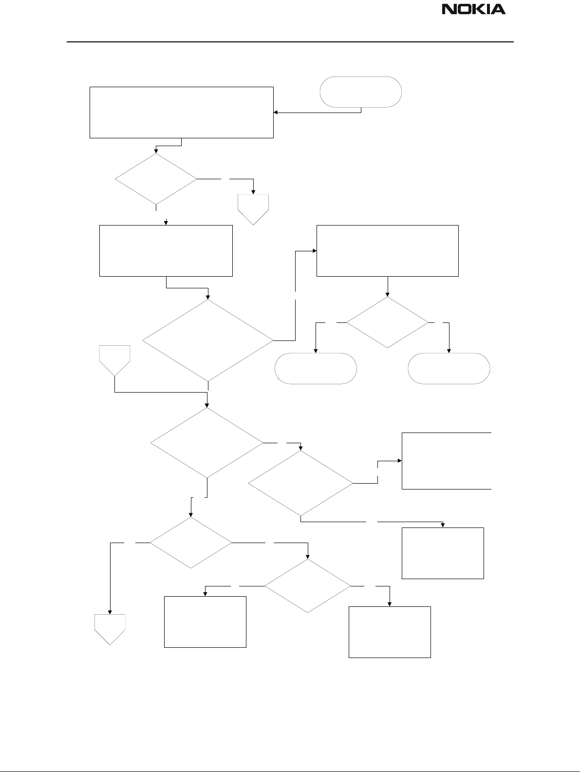
Phone is totally dead.
Measure voltage at N101
pin 5 (VBAT)
3.6V
No
Failure in VBAT.
Check X101, X102, L710
Voltages OK?
Yes
Yes
Measure voltage at V109 pin 4 (Vbb)
2.8V
C112 (VXO) 2.8V
When PWR switch is pressed or
WDOGDISABLE is grounded.
No
Measure voltage at V103
pin 1
3.6V
No
Faulty PCB
Measure voltage at R413 (end
towards CCONT) when pwr-switch
(X400 pin 7) is pressed or
WDOGDISABLE (X201 pin 11) is
grounded.
Yes
Power doesn't stay on.
Faulty PCB
Figure 1: Fault Finding for Totally Dead Phone
Flash Programming Doesn’t Work
The flash programming can be done via panel connector X201 or via system connector
X200.
In production, the first programming is done via panel conne ctor X201. After this, the
panel connector is cut away, thus other flash programming must be done via system
connector X200.
Yes
(Will be low only during power-
0V
up of CCONT if power switch is
pressed.)
No
Check R413, V410
Check LCD-module
Check WDOGDISABLE line
Page 6 Nokia Mobile Phones Ltd. Issue 1 03/01
Page 7

NSB-5
PAMS Technical Documentation Troubleshooting Instructions
The main differences between these are:
• FLASH programming voltage (Vpp) is produced a different way, and
• Signal routings are different.
The fault-finding diagrams for flash programming are shown in Figure 2, Figure 3, and
Figure 4.
In cases of flash programming errors, the flash prommer can provide some information
about a fault. The fault information messages could be:
• MCU doesn’t boot
• Serial clock line failure
• Serial data line failure
• External RAM fault
• Algorithm file or alias ID don’t find
• MCU flash Vpp error
Issue 1 03/01 Nokia Mobile Phones Ltd. Page 7
Page 8
NSB-5
Troubleshooting Instructions PAMS Technical Documentation
FLASH Programming
Check if fault information from Prommer is one of the
following:
a) MCU doesn't boot
b) serial dataline failure
c) serial clock line failure
doesn't work.
failure is one of the
above mentioned?
Yes
Connect watchdog disable (WDDIS R413
end towards N100) to GND.
C308 end away from B400 buzzer
C112 end towards N100 is 2.8V
and
C
Yes
Master RESET PURX (R129)
is "1" (2.8V) after ca. 60ms
Yes
No
A
X201 pin 11 -> R413 end towards N100
No
See section "Phone is
totally dead".
No
Check sleep clock
(C150 end towards D300 or
probe test point J301)
32kHz square wave
Check WDDIS line:
R413 other end -> X400 pin 7
and
Line OK?
No
Check sleep clock circuit.
R117, R118, R126, C103,
C104, C150 and B100
NoYes
Faulty PCB
Yes
Yes
B
13MHz clock
R835 (end away from
D350) 500mVpp min.
Check C760, R706, R707,
V702, R717, C722, L701,
G701
No
No Yes
13MHz clock C300
(end away from D350)
800mV min.
Check R835, C820
Faulty N100 or overloaded
PURX line
Figure 2: Fault Finding for Flash Programming Errors
Page 8 Nokia Mobile Phones Ltd. Issue 1 03/01
Page 9

NSB-5
PAMS Technical Documentation Troubleshooting Instructions
B
FCLK (MBUS) line: X200 pin 11, X201 pin 3 -> V102 pin 5
FTX (fbus_tx) line: X200 pin 13, X201 pin 1 -> V101 pin 5
FRX (fbus_rx) line: X200 pin 12, X201 pin 2 -> V101 pin 4
Check also pull-up and -down resistors: R106, R306, R307
Check that the following lines are OK:
GND: X200 pin 14, X201 pin 7 -> GND
OK? Repair or defective PCB
Yes
MAD or FLASH faulty.
No
Figure 3: Fault Finding for Flash Programming Errors (Cont’d)
Issue 1 03/01 Nokia Mobile Phones Ltd. Page 9
Page 10

NSB-5
Troubleshooting Instructions PAMS Technical Documentation
A
External RAM fault?
Yes
Check pins of SRAM (D302)
Check control lines of SRAM: RAMselX ...
No
Unknown fault.
Try phone totally dead.
No
ID problem?
NO
MCU FLASH Vpp
Error
Yes
Check type of FLASH
Check soldering of FLASH
(Both FLASHES)
Yes
Flashing from X201?
YesNo
Check R302 and R303 in
both ends.
Voltage higher than
1.7V during flashing?
Yes
Defect FLASH or flashing-
SW has wrong version.
No
Defective MAD
MCUGENIO03 or flashing-
SW has wrong version.
Figure 4: Fault Finding for Flash Programming Errors (Cont’d)
Check Vpp: X201 pin 10
to R303 (end towards
D301). Check Vpp_GND
from X201 pin 7 to R303
(other end). Check D100
Page 10 Nokia Mobile Phones Ltd. Issue 1 03/01
Page 11

NSB-5
PAMS Technical Documentation Troubleshooting Instructions
Power Doesn’t Stay on or Phone is Jammed
If this kind of fault occurs after flash programming, th ere may be open pins on ICs or
other discrete components. Solder joints on discrete c apacitors and resistors and open
joints on components with pins, such as D302 (SRAM), should be checked first. The soldered joints of ICs D300 (MAD2WD1), D301 and D303 (FLASH), N200 (COBBA_GJP), and
N100 (CCONT) are difficult to visually inspect since these components are CSP or uBGA
style packages.
A quick and easy way to test the solder joints on CSPs is to apply a small amount of pressure to the top of the package while powering-up the phone. If the phone powers-up
while applying pressure to a specific component (e.g., MAD), then it can be assumed that
that component has faulty solder joints.
Normally, the power will be switched off by CCONT (N100) after 30 seconds if the
watchdog of the CCONT cannot be served by software. In order to verify if watchdog is
updated, verify that X400 pin-2 is high and at the same time X400 pin-13 toggles. In
normal cases, there is a short burst of pulses every 8 seconds.
The power-off function of CCONT can be prevented by connecting a short circuit wire
from R413 (end towards N100) to ground.
Issue 1 03/01 Nokia Mobile Phones Ltd. Page 11
Page 12

NSB-5
Troubleshooting Instructions PAMS Technical Documentation
Power doesn't stay on or
phone is jammed
Check X400 pin 13 while
X400 pin 2 is high
Software is able to run in phone. Check
pin 13 pulsing?
No
Yes
If power is switched off in a few seconds,
check BSI and BTEMP lines.
UI-module.
Connect R413 (end
towards N100) to GND
C308 (end away from B400
buzzer) = 2.8V
and C112 (end towards N100) =
2.8V
Yes
C
No
Vbatt is correct 3.6V
Yes
N100 is faulty.
Figure 5: Power Won’t Stay on or Jammed Phone
The label “C” refers to Figure 2.
Display Information: Contact Service
This fault means that software is able to run and thus, the watchdog of CCONT (N100)
can be served.
Self-test functions are run when power is swit ched on and software has started to execute from flash. If any of the self-tests fail, contact service information will be shown on
Page 12 Nokia Mobile Phones Ltd. Issue 1 03/01
Page 13

NSB-5
PAMS Technical Documentation Troubleshooting Instructions
the display. This may indicate open solder joints on components, faulty PCB, or other
damage to the phone has occurred.
“Contact Service” may also indicate that the flash software has become corrupted. The
phone may then require either a simple re-flash or, in some cases, a total erase and
re-flash.
Phone Doesn’t Register to the Network or Phone Doesn’t Make a Call
If the phone doesn’t register to the network or the phone doesn’t make a call, the reason
could be either a baseband or RF part.
Wintesla service software can be used to set the required mode and determine if the
fault is in the RF or baseband sections (RF interface measurements).
The control lines for the RF section supply both the System ASIC (MAD2;D300) and the
RFI (Cobba_GJP; N200). MAD2WD1 handles digital control lines (synthena, TxP, etc.) and
Cobba handles analog control lines (AFC, TxC, etc.)
The DSP software is constructed so that operation states of DSP (MAD2WD1) can be seen
in external flag (DSPXF) output pin J314.
After power-up, DSP signals all completed functions by changing the state of the XF pin
(see Figure 6, Figure 7, Figure 8, and Figure 9).
1. DSP initialization
2.Synchronization to
network done
3. Registrarition to
network done.
1 2 3
MAD2WD1 pin D8
(DSPXF)
J314
Figure 6: The states of DSP (MAD2) after power on
Issue 1 03/01 Nokia Mobile Phones Ltd. Page 13
Page 14

NSB-5
Troubleshooting Instructions PAMS Technical Documentation
init
initialize
channel
scan starts
1
patch code
download
dsp
constants
download
initializatio
done
Figure 7: The states of DSP after power on
2
PSW
search last PSW
OK
synchronizatio
OK
MAD2WD1 pin D8
(DSPXF)
J314
MAD2WD1 pin D8
(DSPXF)
send RACH
RACH OK
Figure 8: The states of DSP after power on
3
go SDCCH
imediate
OK
J314
MAD2WD1 pin D8
(DSPXF)
J314
Figure 9: The states of DSP after power on
Page 14 Nokia Mobile Phones Ltd. Issue 1 03/01
Page 15

NSB-5
PAMS Technical Documentation Troubleshooting Instructions
Phone doesn't register to the network
phone doesn't make a call
Analog supply voltage to
Check:
Supply voltage Vcp (C126) > 4.8V
Supply voltage VRX_1 (C108) > 2.7V
Supply voltage VRX_2 (C137) > 2.7V
Supply voltage VSYN_2 (C136) > 2.7V
during the receiving slot
Supply voltage VTX (C141) > 2.7V
during the transmitting slot
or
COBBA is > 2.7V?
(C201)
Yes
Analog reference to
COBBA is 1.5V?
(C200)
Yes
No
Check N100
No
Check R200, C140, C167
All OK?
Yes
No
Check N100, D300
D
Figure 10: Fault Finding for Network Registration or Call Problems
Issue 1 03/01 Nokia Mobile Phones Ltd. Page 15
Page 16

NSB-5
Troubleshooting Instructions PAMS Technical Documentation
D
RF control lines:
AGC (R610) 0->2.3Vmax during receiving slot
AFC (C720) 0- 1.2V typ. during receiving slot
OK?
Yes
Analog data signals:
RxIP & RxIN (C640, C641) 0->1.5V DC during
receiving slot
Recieved signal is biased to DC, amplitude 50mVpp
nominal and frequency 13MHz
OK?
Yes
RF control line:
TxC (C524) 0->2.3Vmax during transmit slot
OK?
No
Check N200
No
Check N200 if DC fail
or
RF part
Yes
Analog data signals:
TxIN & TxIP (C525) 0->0.8V DC during transmit slot
No
Check N200 if TxC fail
else
Check D300
Check RF part Check N200
TxQN & TxQP (C526) 0->0.8V DC during transmit slot
Transmit signal is biased to DC, amplitude 300mVpp and
frequency 64kHz
OK?
NoYes
Figure 11: Fault Finding for Network Registration or Call Problems (Cont’d)
Page 16 Nokia Mobile Phones Ltd. Issue 1 03/01
Page 17

NSB-5
PAMS Technical Documentation Troubleshooting Instructions
SIM Card is Out of Order
The hardware for the SIM interface from MAD2WD1 (D300) to the SIM connector (X100)
can be tested without a SIM card.
When the power is switched on and if the BSI line (X102;1) is grounded by a resistor, all
of the used lines (VSIM, RST, CLK, DATA) rise up to 5V four times. Thus, “Insert SIM card”
faults can be found without a SIM card.
The fault information “Card rejected” means that the ATR message (the first message is
always sent from card to phone) is sent from the card to the phone, but the message is
somehow corrupted, data signal levels are wrong, etc., or factory set values stored to the
EEPROM are not correct.
Issue 1 03/01 Nokia Mobile Phones Ltd. Page 17
Page 18

NSB-5
Troubleshooting Instructions PAMS Technical Documentation
Insert SIM card fault
Voltage < 1.5V on top of
R123 when BSI resistor is
connected
No
VSIM (C143), DATAO (C131),
SIMRSTO (C130) and SIMCLKO
(C129) lines rise up to 5V after power
on
No
SIMPWR (J318), DATAA (J303),
SIMRSTA (J315), SIMCLK (J316),
SIMIOC (J317) rise to 2.8V after power
on
Yes
Check X102, R115, R123,
C119
Yes
Check X100, R120
Yes
Faulty PCB, N100
No
Faulty D300
Figure 12: Fault Finding for “Insert SIM Card” Error
Page 18 Nokia Mobile Phones Ltd. Issue 1 03/01
Page 19

NSB-5
PAMS Technical Documentation Troubleshooting Instructions
Card rejected fault
VSIM according to spec.
2.8Vmin (3V card)
4.5Vmin (5V card)
Yes
ATR data can be seen
at C131
Yes
ATR data can be seen
SIM_IOControl line (J317) is
"1" during ATR message
at J303
Yes
Yes
No
Faulty PCB, N100
No
Check X100, R120
No
Check N100
No
Check D300
Check D300
Figure 13: Fault Finding for Rejected SIM Card
Issue 1 03/01 Nokia Mobile Phones Ltd. Page 19
Page 20

NSB-5
Troubleshooting Instructions PAMS Technical Documentation
Audio failure: Uplink (microphone) and downlink (earphone) are broken
Uplink and downlink are
broken
Voltage over C113
(HOOKDET) is 2.8V without
external audio devices
Yes
Voltage over C110
(HEADDET) is 2.8V without
external audio devices
Yes
No
Check R113, R112, C113,
C176
No
Check R110, R109, R108,
C110
Frequency at E501 (PCMSclk)
is 8kHz square wave logical
level during call
Yes
Check for uplink and for
downlink broken
Figure 14: Fault Finding for Broken Uplink and Downlink Audio
No
Check N200
Page 20 Nokia Mobile Phones Ltd. Issue 1 03/01
Page 21

NSB-5
PAMS Technical Documentation Troubleshooting Instructions
Audio failure: Uplink (microphone) is broken
Uplink is broken
Voltage at E101 is 1.8V
Voltage at E100 is 0.3V
during call
Yes
Voltage on COBBA side of
C117 & C121 is 1.4V during call
Yes
Audio voltage (few
millivolts) on COBBA side of
C117 & C121 during call
No
Check:
microphone connections (through slide)
micbias components (V111, R148, R116,
R119, V100)
Micbias control line (one side of R149)
during call
No
Check N200 COBBA
No
Check C117, C121 and
PCB
Yes
Check N200
Figure 15: Fault Finding for Broken Uplink Audio with Working Downlink
Issue 1 03/01 Nokia Mobile Phones Ltd. Page 21
Page 22

NSB-5
Troubleshooting Instructions PAMS Technical Documentation
Audio failure: Downlink (earphone) is broken
Downlink broken
Voltage on C203 & C204 is
1.4VDC
during call
Yes
No
Check R202, C203, C204,
C404, C405, X400 and
N200
Audio signal on C203 & C204
during call when speaker should
emit sound
Yes
Is connector on
Display assy OK?
Yes
Check display module and
speaker
Figure 16: Fault Finding for Broken Downlink with Working Uplink
No
Check N200 & D300
No
Repair or new module
Page 22 Nokia Mobile Phones Ltd. Issue 1 03/01
Page 23

NSB-5
PAMS Technical Documentation Troubleshooting Instructions
Charger Failure
Nothing happens when
charger is connected
Voltage level at R104 is higher
than 0.4V when charger is
connected
Yes
No
Check X200, F100, R101,
L100, C111, C101, R103,
R104
Check N100
Figure 17: Fault Finding for Charger Failure
Issue 1 03/01 Nokia Mobile Phones Ltd. Page 23
Page 24

NSB-5
Troubleshooting Instructions PAMS Technical Documentation
Display information:
Not charging
Voltage at C119 is about
0.8V, power on, BSI
value 39k
Yes
Voltage at C120 is about
0.5V, power on, BTEMP
value 47k
Yes
32Hz (fast charger) or 1Hz
(slow charger) at N101
(CHAPS) pin 7
Yes
No
Check X102, R115,
R123, C119
No
Check X101, R105,
V105, R124, C105,
R115, R123, C120
No
Check R100, N100
N101 pin 5 & 12
same voltage as
No
Vbatt
Yes
Check R102, N101
voltage at N101 pin 5 &
12 rises when charger is
No
connected
Check N101
Yes
Check PCB
Figure 18: Fault Finding for Charger Failure (Cont’d)
Page 24 Nokia Mobile Phones Ltd. Issue 1 03/01
 Loading...