

Page 1

Programmes After Market Services
NSB-5 Series Transceivers
System Module
Issue 1 03/01 Nokia Mobile Phones Ltd.
Page 2

NSB-5
System Module PAMS Technical Documentation
Page 2 Nokia Mobile Phones Ltd. Issue 1 03/01
Page 3

NSB-5
PAMS Technical Documentation System Module
Contents
Page No
System Connector ........................................................................................................ 7
DC Connector ............................................................................................................. 9
Slide Microphone ........................................................................................................ 9
Slide Connector ...........................................................................................................9
Roller Interface ........................................................................................................... 9
Keys and Keymatrix ................................................................................................... 9
Headset Connector ...................................................................................................... 9
Battery Connector ......................................................................................................15
Vibra Alerting Device............................................................................................. 16
SIM Card Connector ..................................................................................................16
Infrared Transceiver Module .................................................................................... 17
Real Time Clock ....................................................................................................... 18
Baseband Module....................................................................................................... 18
Technical Summary .................................................................................................. 18
Power Distribution .................................................................................................... 20
Power Up .................................................................................................................. 22
Power up with a charger.......................................................................................... 22
Power Up With the Power Switch (PWRONX)...................................................... 22
Power Up by RTC....................................................................................................23
Power Up by IBI ..................................................................................................... 23
Acting Dead............................................................................................................. 23
Active Mode............................................................................................................ 23
Sleep Mode.............................................................................................................. 23
Battery charging...................................................................................................... 24
Startup Charging ..................................................................................................... 25
Battery Overvoltage Protection.............................................................................. 25
Battery Removal During Charging ......................................................................... 26
Different PWM Frequencies (1Hz and 32 Hz)........................................................ 27
Battery Identification............................................................................................... 28
Battery Temperature................................................................................................ 29
Supply Voltage Regulators...................................................................................... 29
Audio Control ........................................................................................................... 30
Internal Microphone and Earpiece......................................................................... 31
External Audio Connections .................................................................................. 32
Analog Audio Accessory Detection....................................................................... 32
Internal Audio Connections ................................................................................... 33
4–wire PCM Serial Interface................................................................................... 33
Speech Processing.................................................................................................. 34
Alert Signal Generation........................................................................................... 34
Digital Control ...........................................................................................................34
MAD2WD1............................................................................................................. 34
MAD2PR1 pinout .................................................................................................. 35
Memories .................................................................................................................. 46
Program Memory 32MBit Flash............................................................................. 47
SRAM Memory...................................................................................................... 47
EEPROM Emulated in FLASH Memory............................................................... 47
MCU Memory Requirements ................................................................................... 47
Issue 1 03/01 Nokia Mobile Phones Ltd. Page 3
Page 4

NSB-5
System Module PAMS Technical Documentation
Flash Programming ................................................................................................... 47
IBI Accessories ......................................................................................................... 48
Phone Power–on by IBI ......................................................................................... 48
IBI power–on by phone.......................................................................................... 49
RF Module.................................................................................................................. 50
RF Frequency Plan ................................................................................................... 50
DC Characteristics ................................................................................................... 50
Power Distribution Diagram ..................................................................................... 50
Control Signals ...................................................................................................... 53
Regulator Specifications ........................................................................................... 53
Functional Description ............................................................................................. 54
RF Block Diagram .................................................................................................... 54
Receiver .................................................................................................................... 55
Transmitter ................................................................................................................ 56
Power Detection Circuit ........................................................................................... 57
Frequency Synthesizers ............................................................................................ 60
AGC .......................................................................................................................... 61
AFC ........................................................................................................................... 62
Software Compensations .......................................................................................... 62
Power Levels (TXC) vs. Channel .......................................................................... 62
Modulator Output Level ........................................................................................... 62
Power Levels vs temperature .................................................................................... 62
RSSI .......................................................................................................................... 62
TX power range ........................................................................................................ 62
PA select function ..................................................................................................... 63
RF Block Specifications............................................................................................ 63
GSM1900 Duplex Filter ........................................................................................... 64
Receiver Blocks ......................................................................................................... 65
LNA in CRFU_2a ..................................................................................................... 65
GSM1900 Receive Interstage Filter ......................................................................... 65
First Mixer (UHF) in CRFU_2a ............................................................................... 66
First IF Filter.............................................................................................................. 67
Second Mixer (VHF) in CRFU_2a ........................................................................... 67
Second IF Filter ........................................................................................................ 68
AGC and Third Mixer in SUMMA .......................................................................... 69
Third IF Filter ........................................................................................................... 70
Third IF Buffer in SUMMA ..................................................................................... 70
Transmitter Block..................................................................................................... 70
IQ Modulator and TX AGC in SUMMA ................................................................. 70
Upconversion Mixer and Buffer in CRFU_2a .......................................................... 72
GSM1900 TX SAW Filter ........................................................................................ 73
TX Buffer............................................................................................................... 73
GSM1900 TX Ceramic Filter................................................................................. 73
Power Amplifier MMIC ............................................................................................74
Directional Coupler................................................................................................ 76
Power Detector ......................................................................................................... 76
Power Control Section in SUMMA, Closed Loop Characteristics .......................... 76
Synthesizer Blocks .................................................................................................... 77
Page 4 Nokia Mobile Phones Ltd. Issue 1 03/01
Page 5

NSB-5
PAMS Technical Documentation System Module
VC(TC)XO, Reference Oscillator.......................................................................... 77
VHF PLL in SUMMA .............................................................................................. 78
VHF VCO and Lowpass Filter............................................................................... 79
UHF PLL .................................................................................................................. 80
GSM1900 UHF VCO module .................................................................................. 81
UHF LO signal into CRFU_2a ................................................................................. 82
Data Interface and Timing .........................................................................................83
Synthesizer Timing Control ...................................................................................... 84
Transmit Power Timing ............................................................................................ 86
Interfacing ................................................................................................................. 86
User Interface............................................................................................................. 87
LEDs ......................................................................................................................... 87
Plastic Window ......................................................................................................... 88
Dust Seal ................................................................................................................... 88
LCD Adhesive .......................................................................................................... 88
Reflector ................................................................................................................... 88
Connector .................................................................................................................. 88
Light Guide ............................................................................................................... 88
UI Module Connection to Main PCB ....................................................................... 90
Parts Lists .................................................................................................................. 92
System Module (0201192) ...................................................................................... 92
Issue 1 03/01 Nokia Mobile Phones Ltd. Page 5
Page 6

NSB-5
System Module PAMS Technical Documentation
List of Figures
Page No
Figure 1: System Connector - module .......................................................................7
Figure 2: System Connector - detailed ..................................................................... 8
Figure 3: Combined headset, system connector audio signals ............................... 15
Figure 4: Battery connector locations .................................................................... 16
Figure 5: SIM Card Reader Ultra phone .................................................................16
Figure 6: IR tramsmission frame - example ........................................................... 18
Figure 7: Block Diagram .........................................................................................19
Figure 8: Baseband power distribution .................................................................. 20
Figure 9: Battery Charging ......................................................................................24
Figure 10: Battery Identification ............................................................................ 28
Figure 11: Battery Temperature ............................................................................. 29
Figure 12: Audio Control ....................................................................................... 31
Figure 13: Combined headset and system connector audio signal ......................... 32
Figure 14: IBI power on ..........................................................................................49
Figure 15: RF frequency plan ................................................................................. 50
Figure 16: RF power distribution: maximum currents ........................................... 51
Figure 17: RF power distribution: typical currents ................................................ 52
FIGURE 18: Power Control Loop ......................................................................... 60
FIGURE 19: Phase Control Loop .......................................................................... 61
Figure 20: UI module assembled ........................................................................... 87
Figure 21: Mounting of LEDs for backlight (seen from underside) ...................... 88
Figure 22: Light guide ............................................................................................ 89
Figure 23: Marking specification for the light guide ............................................. 89
Page 6 Nokia Mobile Phones Ltd. Issue 1 03/01
Page 7
NSB-5
PAMS Technical Documentation System Module
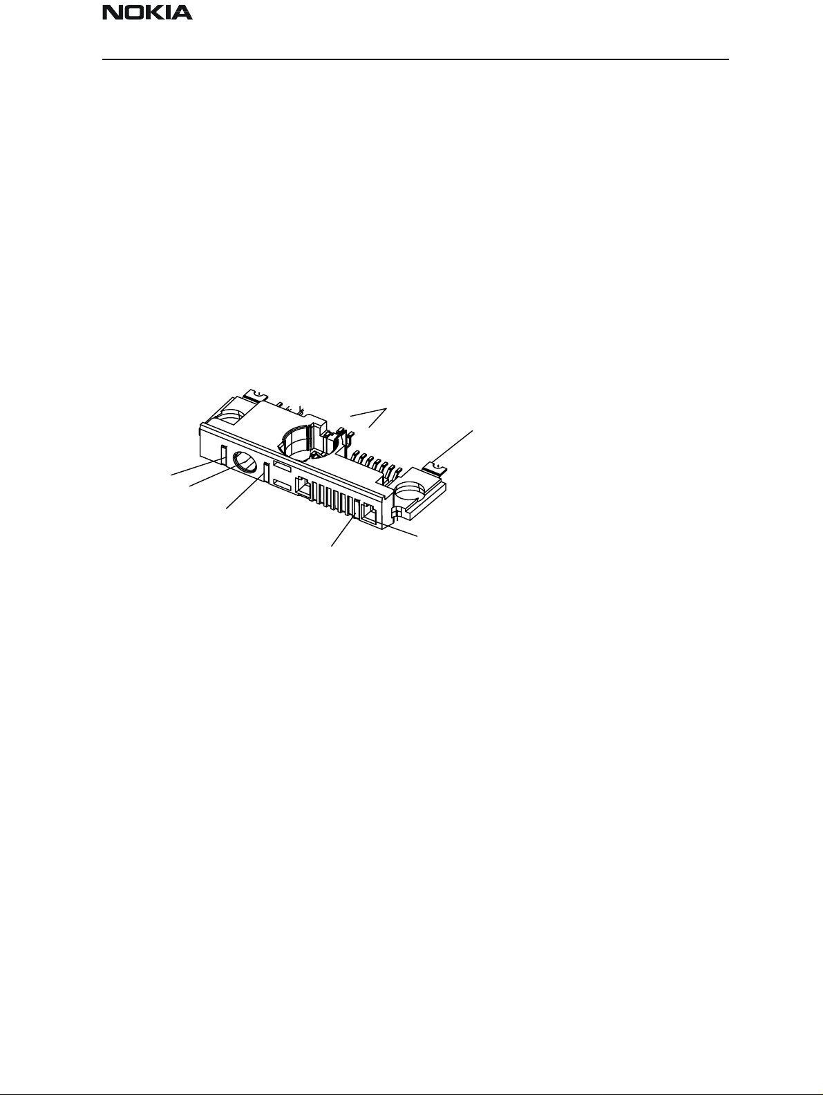
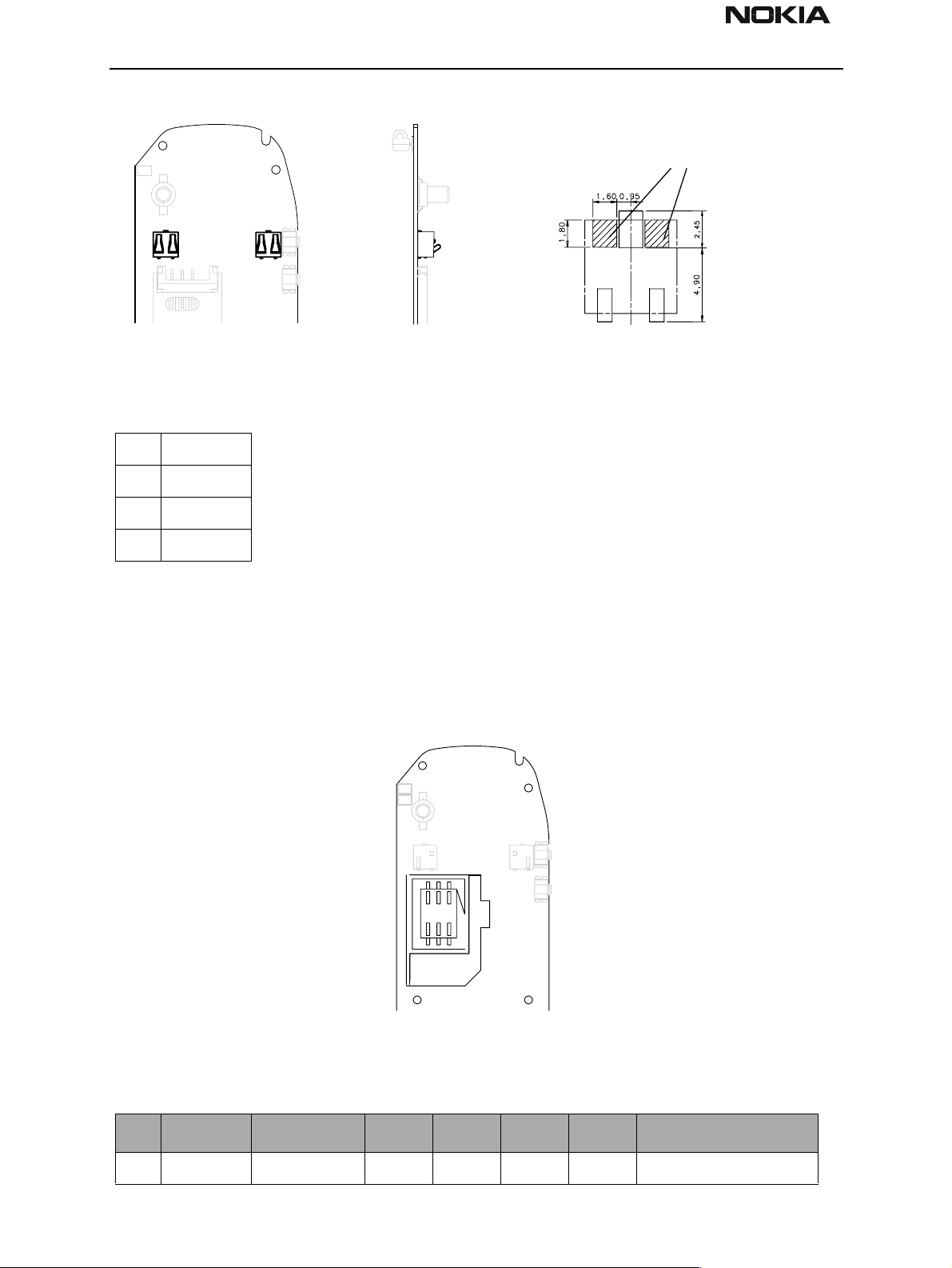
System Connector
This section describes the elect rical connection and interface levels between the baseband, RF and UI parts. The electrical interface specifications are collected into tables that
cover a connector or a defined int erface.
The system connector includes the following parts:
– DC connector for external plug–in charger and a desktop charger
– System connector for accessories and intelligent battery packs
The System connector is used to connect the transceiver to accessories.
System connector pins can be used to connect intelligent battery packs to the trans-
ceiver.
Contact 1
DC–jack
2,3,4
Contact 5
2
3
Slide Detect
4
Contacts
8...13
6
7
8
13
Contact 14
Figure 1: System connector module
Solderable element,
14
Cable/Cradle connector
guiding/fixing hole, 2 pcs
2 pcs
Issue 1 03/01 Nokia Mobile Phones Ltd. Page 7
Page 8
NSB-5
System Module PAMS Technical Documentation
IBI connector
(6 pads)
B side view
14
8
Fixing pads (2 pcs)
1
7
PCB
DC Jack
Microphone
acoustic ports BB
Bottom
connector (6 pads)
A
B
Charger pads (3 pcs)
A side view
Cable locking holes (3 pcs)
Figure 2: System Connector - detailed
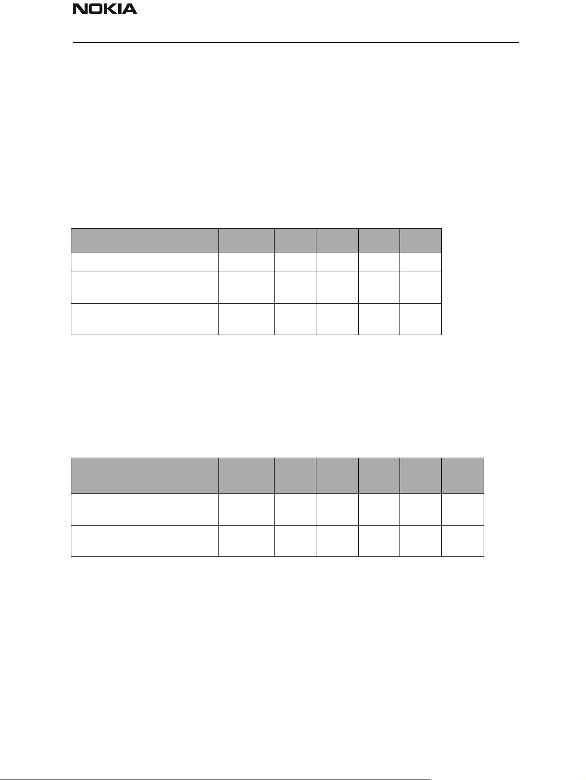
Table 1: System connector signals
Pin Name Function Description
1 V_IN Bottom charger contacts Charging voltage
2 L_GND DC Jack Logic and charging ground
3 V_IN DC Jack Charging voltage
4CHRG_CTRLDC Jack Charger control
5CHRG_CTRLBottom charger contacts Charger control
6 MIC-P Slide Detect Holder Slide Detect
7 MIC-N Slide Detect Holder Gnd
8 XMIC Bottom & IBI connectors Analog audio input
9 SGND Bottom & IBI connectors Audio signal ground
10 XEAR Bottom & IBI connectors Analog audio output
11 MBUS Bottom & IBI connectors Bidirectional serial bus
12 FBUS_RX Bottom & IBI connectors Serial data in
13 FBUS_TX Bottom & IBI connectors Serial data out
14 L_GND Bottom charger contacts Logic and charging ground
Page 8 Nokia Mobile Phones Ltd. Issue 1 03/01
Page 9
NSB-5
PAMS Technical Documentation System Module
DC Connector
The electrical specifications in Table 3 shows the idle voltage produced by the acceptable
chargers at the DC connector input. The absolute maximum input voltage is 18V due to
the transient suppressor that is protecting the charger input.
Slide Microphone
The microphone is connected to the slide by means of springs it has a microphone input
level specified in Table 2. The microphone requires bias current to operate which is generated by the COBBA_GJP ASIC.
Slide Connector
An Interrupt signal to MAD2WD1 determines whether the slide is in an open or closed
position.
Roller Interface
A mechanical solution is implemented and thre e interrupts are fed to the MAD2WD1.
Keys and Keymatrix
0–9, *, #, send, end, soft_1, soft_2, power_on_off, rolle r_push,
Headset Connector
The external headset device is connected to the system connector, from which the signals are routed to COBBA_GJP microphone inputs and earphone outputs.
NA MICN mounted in
slide
NA MICP mounted in
slide
Table 2: Mic signals of the system connector
0 2 12.5 mV Connected to COBBA_GJP MIC2N input. The
maximum value corresponds to 1 kHz, 0 dBmO
network level with input amplifier gain set to
32 dB, typical value is maximum value - 16 dB.
0 2 12.5 mV Connected to COBBA_GJP MIC2P input. The
maximum value corresponds to 1 kHz, 0 dBmO
network level with input amplifier gain set to
32 dB, typical value is maximum value - 16 dB.
Issue 1 03/01 Nokia Mobile Phones Ltd. Page 9
Page 10
NSB-5
System Module PAMS Technical Documentation
Table 3: System/IBI connector
IB-
Pin
NAME Function Min Typ Max Unit Description
pin
10 Yes XEAR Analog
audio output (from
phone to
accessory)
Accessory
detection
(from
accessory
to phone)
16
4.7
0
47
10
10
1.0
100
0.5
6.8
300
0.2
V
Ω
Output AC impedance (ref GND)
resistor tol. is 5%
uF
Series output capacitance
Load AC impedance to GND: Head-
Ω
set
Load AC impedance to SGND:
kΩ
External accessory
Max. output level. No load
p-p
Resistance to accessory ground (in
kΩ
accessory)
V
DC voltage (ref. SNGD). External
accessory
Load DC resistance to SGND. Exter-
kΩ
nal accessory
DC voltage (ref SGND). Headset
V
with closed switch
16
2.8
47
1500
Load DC resistance to SNGD. Head-
Ω
set with closed switch
DC voltage (ref SGND). No acces-
V
sory or headset with open switch
Pull-up resistor to VBB in phone
kΩ
Page 10 Nokia Mobile Phones Ltd. Issue 1 03/01
Page 11
NSB-5
PAMS Technical Documentation System Module
Table 3: System/IBI connector
IB-
Pin
NAME Function Min Typ Max Unit Description
pin
8 Yes XMIC Analog
audio input
(from
accessory
to phone)
Headset
microphone
input (from
accessory
to phone)
Accessory
mute. Voltage compared to
SGND.
(from
phone to
accessory)
Headset
detection
(from
accessory
to phone)
(NO TAG)
2.0
100
2.0
2.5
100
2.5
0
1.6 2.0
1.47
0
49
2.2
1
2.2
600
200
2.9
1.55
2.4
2.9
1.33VV
kΩ
Ω
V
kΩ
kΩ
µA
mV
p-p
V
V
V
kΩ
Input AC impedance
Accessory source AC impedance
Maximum signal level
p-p
Input AC impedance
Headset source AC impedance
Bias current
Maximum signal level
Not muted
Muted, without headset
Comparator reference in accessory
No headset (ref SGND)
Headset connected (ref SGND)
Pull-up resistor to VBB in phone
Function
DLR-3
Datacable
Detection
9 Yes SGND Audio sig-
nal ground.
Separated
from
phone GND
(from
phone to
accessory)
440 733 mV DLR-3 detected (ref SGND)
Output AC impedance (ref GND)
Series output capacitance
Resistance to phone ground (DC)
(in phone)
Resistance to accessory ground (in
accessory)
DC voltage compared to phone
GND
DC voltage compared to accessory
GND
-0.2
-5
47
10
380
100
+0.2
+5
Ω
µF
Ω
kΩ
V
V
Issue 1 03/01 Nokia Mobile Phones Ltd. Page 11
Page 12

NSB-5
System Module PAMS Technical Documentation
Table 3: System/IBI connector
IB-
Pin
NAME Function Min Typ Max Unit Description
pin
13 Yes FBUS_TXSerial data
out (from
phone to
accessory)
12 Yes FBUS_RXSerial data
in (from
accessory
to phone)
0.1
1.7
0
2.0
47
220
47
220
47
0.8
2.8
100
150
1
0.8
2.8
V
V
kΩ
kΩ
Ω
pF
µs
V
V
kΩ
kΩ
Output low voltage @ I
GND)
Output high voltage @ I
(ref GND)
Pull-up resistor in phone
Pull-down resistor in accessory
Serial (EMI filtering) resistor in
phone
Cable capacitance
Rise/fall time
Input low voltage (ref GND)
Input high voltage (ref GND)
Pull-down resistor in phone
Pull-up resistor in accessory
<mA (ref
OL
<4mA
OH
2.2
150
2
1
kΩ
pF
µs
µs
Serial (EMI filtering) resistor in
accessory
Cable capacitance
Rise/fall time @ 115kbits/s
Rise/fall time @ 230kbits/s
Page 12 Nokia Mobile Phones Ltd. Issue 1 03/01
Page 13
NSB-5
PAMS Technical Documentation System Module
Table 3: System/IBI connector
IB-
Pin
NAME Function Min Typ Max Unit Description
pin
11 Yes MBUS
FLASH_
CLK
2,
- L_GND Logic and
14
Bidirectional
serial bus
charging
ground
(separated
from
phone GND
by EMI
components)
0
2.0
0
0.8
2.8
0.8
V
V
V
Input low voltage (ref GND)
Input high voltage (ref GND)
Output low voltage @ I
(ref GND)
2.1
2.9
V
Output high voltage @ I
µA (ref GND)
4.7
220
100
kΩ
kΩ
Ω
Pull-up resistor in phone
Pull-down resistor in accessory
Serial (EMI filtering) resistor in
phone
200
5
pF
µs
Cable capacitance
Rise/fall time @ 9600 bits/s
0 1.0 A Ground current
<4mA
OL
OH
<100
4,5 - CHRG_
CTRL
Charger
control
(from
phone to
accessory)
0
1.7
1
32
20
30
0.8
2.9
37
99
V
V
Hz
%
kΩ
kΩ
Output low voltage @ I
Output high voltage @ I
<20 µA
OL
<20 µA
OH
PWM frequency
PWM duty cycle
Serial (EMI filtering) resistor in
phone
Pull-down resistor in phone
Issue 1 03/01 Nokia Mobile Phones Ltd. Page 13
Page 14
NSB-5
System Module PAMS Technical Documentation
Table 3: System/IBI connector
IB-
Pin
NAME Function Min Typ Max Unit Description
pin
1,3 - VIN Fast
charger
(from
accessory
to phone)
Slow
charger
(from
accessory
to phone)00
0
0
8.5
0.85
100
100
100
200
15
V
A
mV
p-p
mV
p-p
mV
p-p
mV
p-p
V
peak
Charging voltage
Charging current
Ripple voltage @ f = 20...200Hz,
load = 3 & 10 Ω
Ripple voltage @ 4 = 0.2...30kHz,
load = 3 & 10 Ω
Ripple voltage @ f > 30kHz, load =
3 & 10 Ω
Total ripple voltage @ f > 20Hz,
load = 3 & 10 Ω
Charging voltage (max . =
unloaded, +20% overvoltage in
mains)
1.0
A
Charging current (max. = shorted,
peak
+20% overvoltage in mains)
Page 14 Nokia Mobile Phones Ltd. Issue 1 03/01
Page 15
NSB-5
PAMS Technical Documentation System Module
Baseband
HOOKDET
MAD
HEADDET
CCONT
EAD
HF
COBBA
–GJP
AUX
OUT
PD2
AGND
10m
10k
100n
AGND
10u
27p
100n
1u
220k
220k
VBB VBB
2k2 47k
2k2
VBB
47k
100MHz
33R
AGND
47R
XEAR
LGND
PC–Board
R01
SW01
+
+
+
C01
C03
C02
HFCM
MIC1N
MIC1P
MIC3N
MIC3P
AGND
Note 1: Grey resistor are in the border of ”EMI clean” and ”dirty” areas.
Note 2: AGND is connected directly to the GND on PCB close to HF parts.
Note 3: ESD protection diodes are not shown.
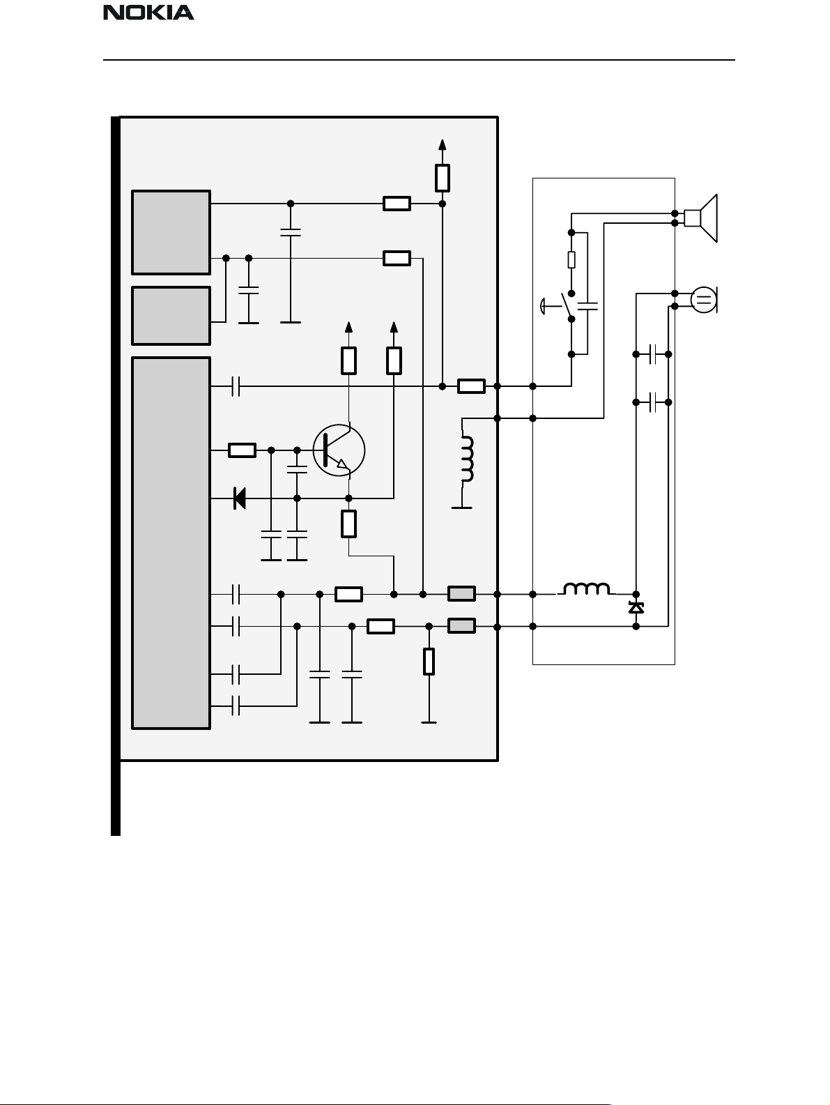
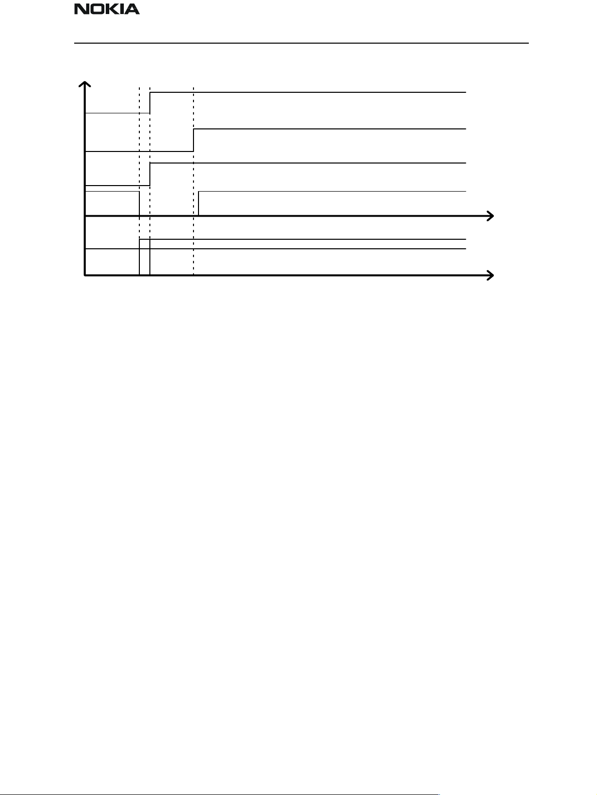
Battery Connector
The BSI contact on the battery co nnector is used to detect when thebattery is removed
with power switched on enabling the SIM card operation to shut down first. The BSI contact in the battery pack should be shorter than the supply power contacts to give enough
time for the SIM shut down.
AGND
27p
2k2
27p
100n
100n
100n
100n
AGND AGND AGND
2k2
100R
100R
330R
XMIC
SGND
R01= 100R
C01=33uF
C02=1000pF
C03=22pF
L01=MMZ2012Y6
01BT/TDK
Figure 3: Combined headset, system connector audio signals
L01
Z01
Issue 1 03/01 Nokia Mobile Phones Ltd. Page 15
Page 16
NSB-5
System Module PAMS Technical Documentation
No metal in these areas!
old connector type
12
B side view.
phone
1+VBATT
2BSI
3BTEMP
4-VBATT
34
Vibra Alerting Device
A special battery pack contains a vibra motor. The vibra is controlled with one PWM signal by the MAD2WD1 via the BTEMP battery terminal.
Figure 4: Battery connector locations
SIM Card Connector
The SIM card connector is located on the PCB. Only small SIM cards are supported.
321
456
Figure 5: SIM Card Reader Ultra phone
Table 4: SIM Connector Electrical Specifications
Pin Name Parameter Min Typ Max Unit Notes
1GND GND 0 0 V Ground
Page 16 Nokia Mobile Phones Ltd. Issue 1 03/01
Page 17
NSB-5
PAMS Technical Documentation System Module
Table 4: SIM Connector Electrical Specifications
Pin Name Parameter Min Typ Max Unit Notes
2 VSIM 5V SIM Card
3V SIM Card
3DATA5V Vin/Vout
3V Vin/Vo ut
4 SIMRST 5V SIM Card
3V SIM Card
5SIMCLK Frequency
Trise/Tfall
6 VPP 5V SIM Card
3V SIM Card
VSIM supply voltages are specified to meet type approval requirements regardless of the
tolerances in components.
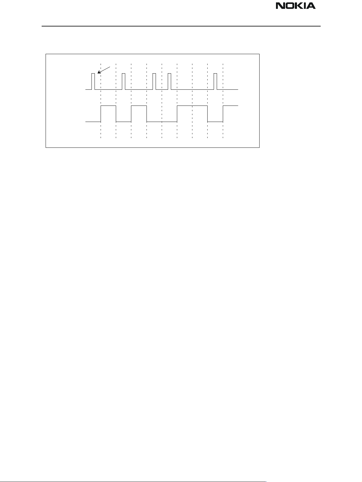
Infrared Transceiver Module
An infrared transceiver module is designed as a substitute for hardwired connections
between the phone and a PC. The infrared transceiver module is a stand alone component. In DCT3 the module is located inside and at the top of the phone.
4.8
2.8
4.0
0
2.8
0
4.0
2.8
4.8
2.8
5.0
3.0
“1”
“0”
“1”
“0”
“1”
“1”
3.25
5.0
3.0
5.2
3.2
VSIM
0.5
VSIM
0.5
VSIM
VSIM
25
5.2
3.2
V Supply voltage
V SIM data
Trise/Tfall max 1 us
V SIM reset
MHz
ns
V Programming voltage
SIM clock
pin6 and pin2 tied
together
The Rx and Tx is connected to the FBUS via a dual bus buffer. The module and buffer is
activated from the MAD2 with a pull up on IRON. The Accif in MAD2 performs pulse
encoding and shaping for transmitted data pulses and detection and decoding for
received data pulses.
The data is transferred over the IR link using serial FBUS data at speeds 9.6, 19.2, 38.4,
57.6 or 115.2 kbits/s, which leads to maximum throughput of 92.160 kbits/s. The used IR
module complies with the IrDA SIR specification (Infra Red Data Association), which is
based on the HP SIR (Hewlett–Packard‘s Serial Infra Red) concept.
Issue 1 03/01 Nokia Mobile Phones Ltd. Page 17
Page 18
NSB-5
System Module PAMS Technical Documentation
The following figure gives an example of IR transmission pulses. In IR transmission, a
light pulse corresponds to 0–bit and a ”dark pulse” corresponds to 1–bit.
constant pulse
IR TX
UART TX
startbit stopbit
The FBUS cannot be used for external accessory communication, when the infrared mode
is selected. Infrared communication reserves the FBUS completely.
Real Time Clock
Requirements for a real time clock implementation are a basic clock (hours and minutes),
a calender and a timer with alarm and power on/off –function and miscellaneous calls.
The RTC will contain only the time base and the alarm timer but all other functions (e.g.
calendar) will be implemented with the MCU software. The RTC needs a power backup to
keep the clock running when the phone battery is disconnected. The backup power is
supplied from a rechargable polyacene battery that can keep the clock running for
approximately ten minutes. If the backup has expired, the RTC clock restarts after the
main battery is connected. The CCONT resets the MCU in approx 62ms and the 32kHz
source is settled (after approx. 1s).
The CCONT is an ideal place for an integrated real time clock as the asic already contains
the power up/down functions and a sleep control with the 32kHz sleep clock, which is
always running when the phone battery is connected. This sleep clock is used for a time
source to a RTC block.
1
0100110
Figure 6: IR tramsmission frame - example
Baseband Module
Technical Summary
The baseband architecture is basically similar to DCT3 GSM phones. DCT3.5 differs from
DCT3 in the single PCB concept and the serial interface between MAD2WD1 and
COBBA_GJP and MAD2WD1 and CCONT. In DCT3.5 the MCU, the system-specific ASIC
and the DSP are intergrated into one ASIC, called the MAD2WD1 chip, which takes care
of all the signal processing and operation controlling tasks of the phone.
The baseband architecture supports a power saving function called ”sleep mode”. This
sleep mode shuts off the VCTCXO, which is used as system clock source for both RF and
baseband. During the sleep mode the system runs from a 32 kHz crystal. The phone is
wakened up by a timer running from this 32 kHz clock supply. The sleeping time is deter-
Page 18 Nokia Mobile Phones Ltd. Issue 1 03/01
Page 19
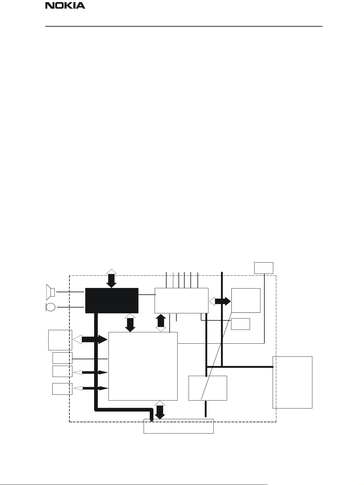
NSB-5
PAMS Technical Documentation System Module
mined by some network parameters. When the sleep mode is entered both the MCU and
the DSP are in standby mode and the normal VCTCXO clock has been switched off.
The battery voltage range in DCT3 family is 3.0V to 4.5V depending on the battery charge
and used cell type (Li–Ion or NiMH). Because of the lower battery voltage the baseband
supply voltage is lowered to a nominal of 2.8V.
The baseband is running from a 2.8V power rail which is supplied by a power controlling
asic (CCONT). In the CCONT there are seven individually controlled regulator outputs for
the RF section, one 2.8V output for the baseband plus a core voltage for MAD2WD1.
However this is not used in NSB–5 because the chipset support s 2.8 Volts. In addition
there is one +5V power supply output(V5V). TheCCONTalso contains a SIM interface
which supports both 3V and 5V SIM cards. A real time clock function is integrated into
the CCONT which utilizes the same 32KHz clock supply as the sleep clock. A backup
power supply is provided for the RTC, which keeps the real time clock running when the
main battery is removed. The backup power supply is a rechargeable polyacene battery
with a backup time of ten minutes.
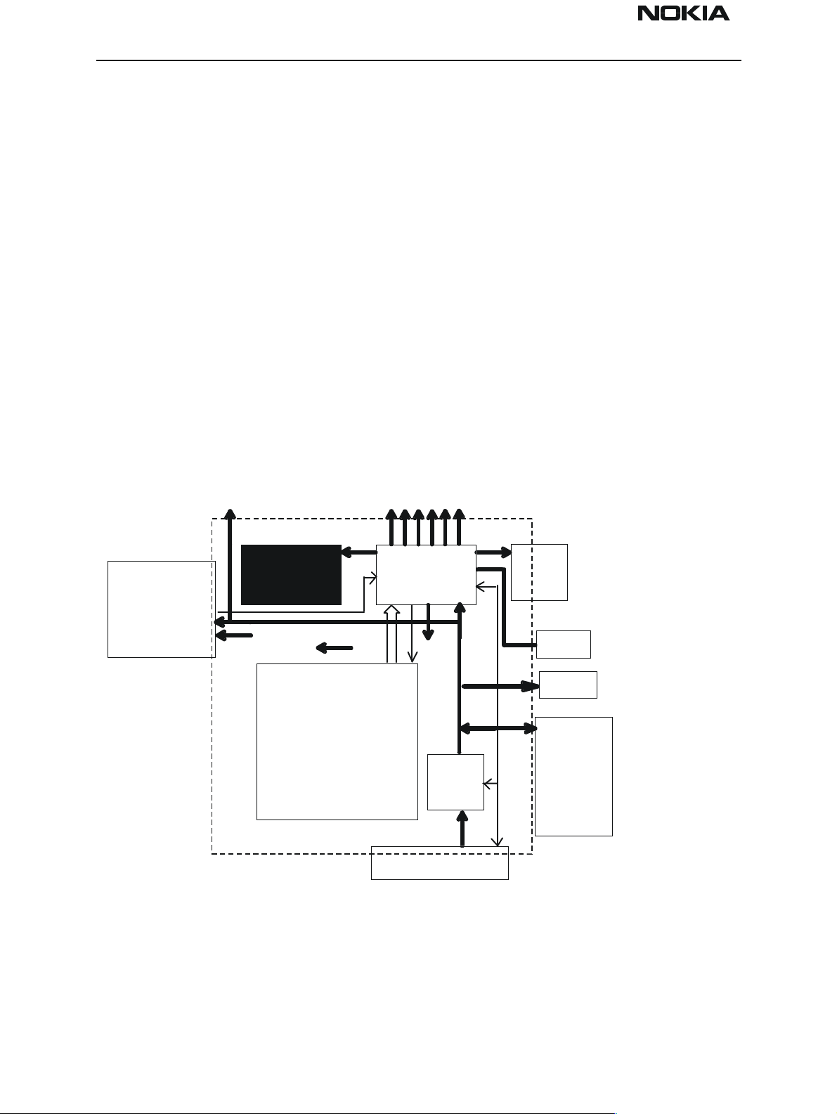
The interface between the baseband and the RF section is handled by a specific asic. The
COBBA_GJP asic provides A/D and D/A conversion of the in–phase and quadrature
receive and transmit signal paths and also A/D and D/A conversions of received and
transmitted audio signals to and from the UI parts. Data transmission between the
COBBA_GJP and the MAD2WD1 is implemented using serial connections. Digital speech
processing is handled by the MAD2WD1 asic. The COBBA_GJP asic is a dual supply voltage circuit, the digital parts are running from the baseband supply VBB and the analog
parts are running from the analog supply VCOBBA (VR6).
LCD
vibra
motor
IR
roller
TX/RX SIGNALS
COBBA SUPPLY
COBBA_GJP
MAD2WD1
+
MEMORIES
RF SUPPLIES
CCONT
BB SUPPLY
core voltage
CHAPS
PA SUPPLY
SIM
32kHz
CLK
SLEEP CLOCK
VBAT
13MHz
CLK
SYSTEM CLOCK
BATTERY
NiMH LiIon
AUDIOLINES
BASEBAND
SYSCON
Figure 7: Block Diagram
Issue 1 03/01 Nokia Mobile Phones Ltd. Page 19
Page 20
NSB-5
System Module PAMS Technical Documentation
Power Distribution
In normal operation the baseband is powered from th e phone‘s battery. The battery consists of one Lithium–Ion cell. There is also a possibility to use batteries consisting of
three Nickel Metal Hydride cells or one solid state cell. An external charger can be used
for recharging the battery and supplying power to the phone. The charger can be either
so called fast charger, which can deliver supply current up to 1600 mA or a standard
charger that can deliver approx 300 mA.
The CCONT provides voltage to th e circuitry excluding the RF PA, LCD, and IrDa, which
are supplied via a continuous power rail direct from the battery. The RF PA module has a
cutoff voltage of 3.1V. The batter y(see note) feeds power directly to several parts of the
system: CCONT, PA, and UI circuitry (display lights, buzzer). The four dedicated control
lines, RxPwr, TxPwr, SIMCardPwr, and SynthPwr from MAD2 to CCONT have changed to a
serial control signal between MAD2WD1 and CCONT. Figure 8 shows a simplified block
diagram of the power distribution.
Note : In battery terms there is VBATT and VB, the difference is a filter (coil and capacitors).
The power management circuitry provides protection against overvoltages, charger failures, and pirate chargers, etc., that could cause damage to the phone.
PA SUPPLY
VCOBBA
COBBA_GJP
LCD
MODULE
VBAT
VBB
MAD2WD1
+
MEMORIES
BASEBAND
RF SUPPLIES
CCONT
PWRONX
CNTVR
VBB
core volta ge
PURX
POWER
MGMT
VIN
VSIM
VBAT
PWM
SIM
RTC
BACKUP
BATTERY
sram
CONNECTOR
Figure 8: Baseband power distribution
The heart of the power distribution is the CCONT. It includes all the voltage regulators
and feeds the power to most of the system. The whol e baseband is powered from the
same regulator which provides 2.8V baseband supply VBB. The baseband regulator is
active always when the phone is powered on. The core baseband regulator feeds,
amongst others, MAD2WD1 and memories, COBBA_GJP digital parts and the LCD driver
in the UI section. COBBA_GJP analog parts are powered from a dedicated 2.8V supply
Page 20 Nokia Mobile Phones Ltd. Issue 1 03/01
Page 21
NSB-5
PAMS Technical Documentation System Module
VCOBBA by the CCONT. There is a separate regulator for a SIM card which is selectable
between 3V and 5V and controlled by the SIMPwr line from MAD2WD1 to CCONT.
The CCONT contains a real time clock function, which is powered from a RTC backup
when the main battery is disconnected. The RTC backup is rechargable polyacene battery.
CCONT includes also six additional 2.8V regulators providing power to the RF section.
These regulators can be controlled by the seriel interface from MAD2WD1; i.e., RF regulator control register in CCONT which MAD2WD1 can update.
CCONT supplies a core voltage to the MAD2WD1. The core voltage is by default 1.975V,
but can be set lower, depending on the MAD2 silicon technology.
RAM_BCK is not used.
CCONT generates also a 1.5 V reference voltage VREF to COBBA_GJP, SUMMA. The VREF
voltage is also used as a reference to some of the CCONT A/D converters and as a reference for al the other regulators.
In addition to the above-mentioned signals, MAD2WD1 includes also TXP control signal
which goes to SUMMA power control block and to the power amplifier. The transmitter
power control TXC is led from COBBA_GJP to SUMMA.
Table 5: CCONT current output capability/nominal voltage
Regulator
VR1 25 mA 2.8 V VCTCXO
VR2 25 mA 2.8 V CRFU Rx
VR3/switch 50 mA 2.8 V PLL VSYN
VR4 90 mA 2.8 V VCO VSYN
VR5 80 mA 2.8 V SUMMA Rx
VR6 100 mA 2.8 V COBBA_GJP
VR7 150 mA 2.8 V SUMMA+CRFU Tx
VBB ON
VBB SLEEP
VSIM 30 mA 3.0/
Maximum
current
125
1
Unit Vout Unit Notes
mA
mA
2.8
2.8
5.0
V
V
V
V
current limit 250mA
current limit 5mA
VSIM
outout voltage selectable
V_core 50 mA 1.975 V programmable core supply for CPU/
DSP/SYS ASIC dV=225V
V_RAM_bck/VR3 50 mA 2.8 V n ormal mode 2.8V. 2.0V for data
retention. (not used)
VSIM must fulfill the GSM11.10 current spike requirements.
Issue 1 03/01 Nokia Mobile Phones Ltd. Page 21
Page 22

NSB-5
System Module PAMS Technical Documentation
VSIM and V5V can give a total of 30 mA.
Power Up
The baseband is powered up by:
1 Pressing the power key, that generates a PWRONX interrupt signal from the
power key to the CCONT, which starts the power up procedure.
2 Connecting a charger to the phone. The CCONT recognizes the charger from the
VCHAR voltage and starts the power up procedure.
3 A RTC interrupt. If the real time clock is set to alarm and the phone is switched
off, the RTC generates an interrupt signal, when the alarm is gone off. The RTC
interrupt signal is con-nected to the PWRONX line to give a power on signal to
the CCONT just like the power key.
4 A battery interrupt. Intelligent battery packs have a possibility to power up the
phone. When the battery gives a short (10ms) voltage pulse through the BTEMP
pin, the CCONT wakes up and starts the power on procedure.
Power up with a charger
When the charger is connected, CCONT will switch on the CCONT digital voltage as soon
as the battery voltage exeeds 3.0V. The reset for CCONT’s digital parts is released when
the operating voltage is stabilized ( 50 us from switching on the voltages). Operating
voltage for VCXO is also switched on. The counter in CCONT digital section will keep
MAD in reset for 62 ms (PURX) to make sure that the clock provided by VCXO is stable.
After this delay, MAD reset is released, and VCXO–control (SLEEPX) is given to MAD. The
diagram assumes empty battery, but the situation would be the same with full battery:
When the phone is powered up with an empty batter y pack using the standard charger,
the charger may not supply enough current for standard power-up procedure and the
powerup must be delayed.
Power Up With the Power Switch (PWRONX)
When the power on switch is pressed the PWRONX signal will go low. CCONT will switch
on the CCONT digital section and VCXO as was the case with the charger-driven power
up. If PWRONX is low when the 64 ms delay expires, PURX is released and SLEEPX control
goes to MAD. If PWRONX is not low when 64 ms expires, PURX will not be released, and
CCONT will go to power off ( digital section will send power off signal to analog parts)
.
Page 22 Nokia Mobile Phones Ltd. Issue 1 03/01
Page 23
NSB-5
PAMS Technical Documentation System Module
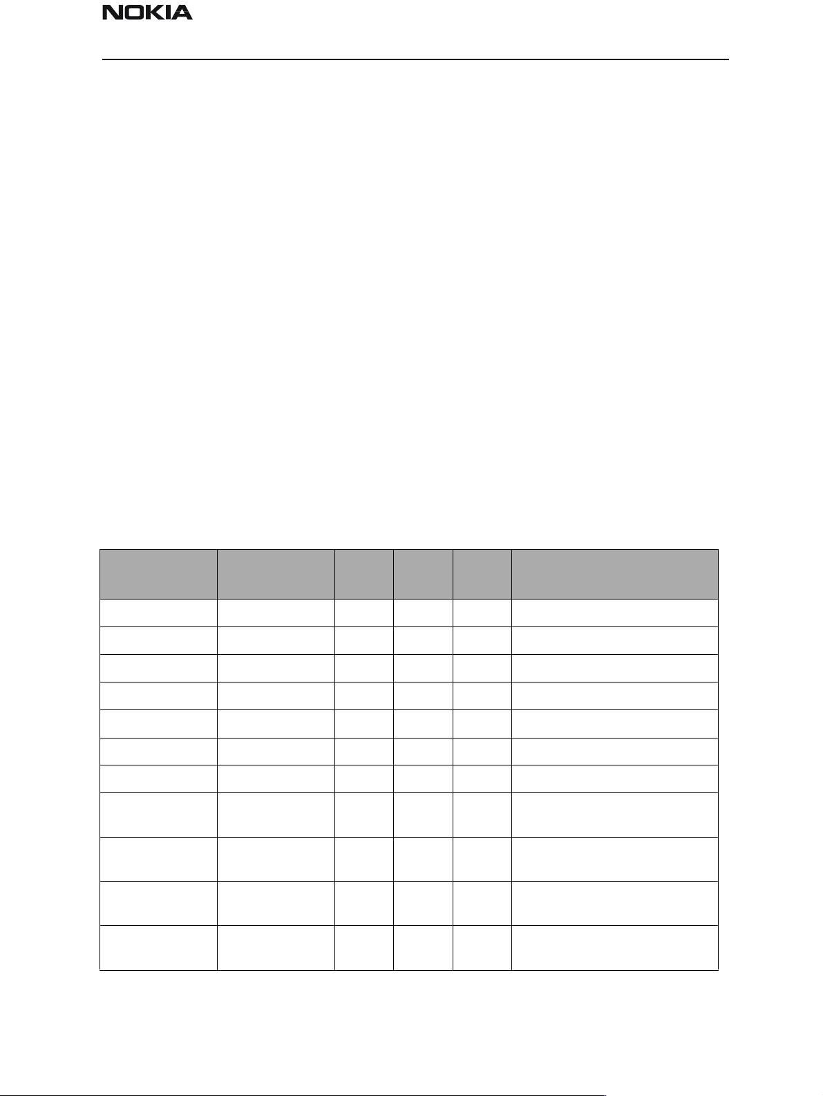
SLEEPX
PURX
CCPURX
PWRONX
VR1,VR6
VBB (2.8V)
Vchar
12 3
1: Power switch pressed ==> Digital voltages on in CCONT (VBB).
2: CCONT digital reset released. VCXO turned on.
3: 62 ms delay to see if power switch is still pressed.
Po wer Up by RTC
RTC ( internal in CCONT) can power the phone up by changing RTCPwr to logical ”1”.
RTCPwr is an internal signal from the CCONT digital section.
Po wer Up by IBI
IBI can power CCONT up by sending a short pulse to logical ”1”. RTCPwr is an internal
signal from the CCONT digital section.
Acting Dead
If the phone is off when the charger is connected, the phone is powered on but enters a
state called ”acting dead”. To the user the phone acts as if it was switched off. A battery
charging alert is given and/or a battery charging indication on the display is shown to
acknowledge the user that the battery is being charged.
Active Mode
In the active mode the phone is in normal operation, scanning for channels, listening to
a base station, transmitting and processing information. All the CCONT regulators are
operating. There are several substates in the active mode depending on if the phone is in
burst reception, burst transmission, if DSP is working etc.
Sleep Mode
In the sleep mode all the regulators except the baseband VBB, Vcore, and the SIM card
VSIM regulators are off. Sleep mode is activated by the MAD2WD1 after MCU and DSP
clocks have been switched off. The voltage regulators for the RF section are switched off
Issue 1 03/01 Nokia Mobile Phones Ltd. Page 23
Page 24
NSB-5
System Module PAMS Technical Documentation
and the VCXO power control, VCXOPwr is set low. In this state only the 32 kHz sleep
clock oscillator in CCONT is running. The flash memory power down input is connected to
the VCXO power control, so that the flash is deep powered down during sleep mode. During sleep mode, the phone wakes up periodically to page the base station for incoming
calls, location update, etc. The paging rate is a parameter set by the BS.
The sleep mode is exited either by the expiration of a sleep clock counter in the
MAD2WD1 or by some external interrupt, gener ated by a charger connection, key press,
headset connection, etc. The MAD2WD1 starts the wake up sequence and sets the VCXOPwr control high. After VCXO settling time other regulators and clocks are enabled for
active mode.
If the battery pack is disconnect during the sleep mode, the CCONT shall power down the
SIM in the sleep mode as there is no time to wake up the MCU.
Battery charging
The electrical specifications give the idle voltages produced by the acceptable chargers
at the DC connector input. The absolute maximum input voltage is 30V due to the transient suppressor that is protecting the charger input. At phone end there is no difference
between a plug–in charger or a desktop charger. The DC–jack pins and bottom connector
charging pads are connected together inside the phone.
MAD
MAD
VBAT
CCONTINT
CCONT
0R22
PWM_OUT
GND
ICHAR
VCHAR
LIM
VOUT
CHAPS
RSENSE
PWM
22k
VCH
GND
1n
27pf
Figure 9: Battery Charging
TRANSCEIVER
33R/100MHz
1u
47k
47k
30V
1.5A
EMI
VIN
CHRG_CTRL
L_GND
CHARGER
NOT IN
ACP–7/8
Page 24 Nokia Mobile Phones Ltd. Issue 1 03/01
Page 25
NSB-5
PAMS Technical Documentation System Module
Startup Charging
When a charger is connected, the CHAPS is supplying a startup current minimum of
130mA to the phone. The startup current provides initial charging to a phone with an
empty battery. Startup circuit charges the battery until the battery voltage level reaches
3.0V (+/– 0.1V) and the CCONT releases the PURX reset signal and program execution
starts. Charging mode is changed from startup charging to PWM charging that is controlled by the MCU software. If the battery voltage reaches 3.55V (3.75V maximum)
before the program has taken control over the charging, the startup current is switched
off. The startup current is switched on again when the battery voltage is sunken
100mV (nominal).
Table 6: Startup Charging Parameters
Parameter Symbol Min Typ Max Unit
VOUT start-up mode cutoff limit Vstart 3.45 3.55 3.75 V
VOUT start-up mode hysteresis
Note: COUT = 4.7µF
Start-up regulator output current
VOUT = 0V ... Vstart
Battery Overvoltage Protection
Output overvoltage protection is used to protect phone from damage. This function is
also used to define the protection cutoff voltage for different battery types (Li or Ni). The
power switch is immediately turned OFF if th e voltage in VOUT rises above the selected
limit VLIM1 or VLIM2.
Table 7: Battery O v ervoltage Protection
Parameter Symbol
Output voltage cutoff limit (during
transmission or Li-battery)
Output voltage cutoff limit (no
transmission or Ni-battery)F
Vstarthys 80 100 200 mV
Istart 130 165 200 mA
LIM
input
VLIM1 LOW 4.4 4.6 4.8 V
VLIM2 HIGH 4.8 5.0 5.2 V
Min Typ Max Unit
The voltage limit (VLIM1 or VLIM2) is selected by logic LOW or logic HIGH on the CHAPS
(N101) LIM– input pin. Default value is lower limit VLIM1.
Issue 1 03/01 Nokia Mobile Phones Ltd. Page 25
Page 26
NSB-5
System Module PAMS Technical Documentation
When the switch in output overvoltage situation has once turned OFF, it stays OFF until
the the battery voltage falls below VLIM1 (or VLIM2) and PWM = LOW is detected. The
switch can be turned on again by setting PWM = HIGH.
VCH
VCH<VOUT
t
VOUT
VLIM1 or VLIM2
t
SWITCH
PWM (32Hz)
ON OFF
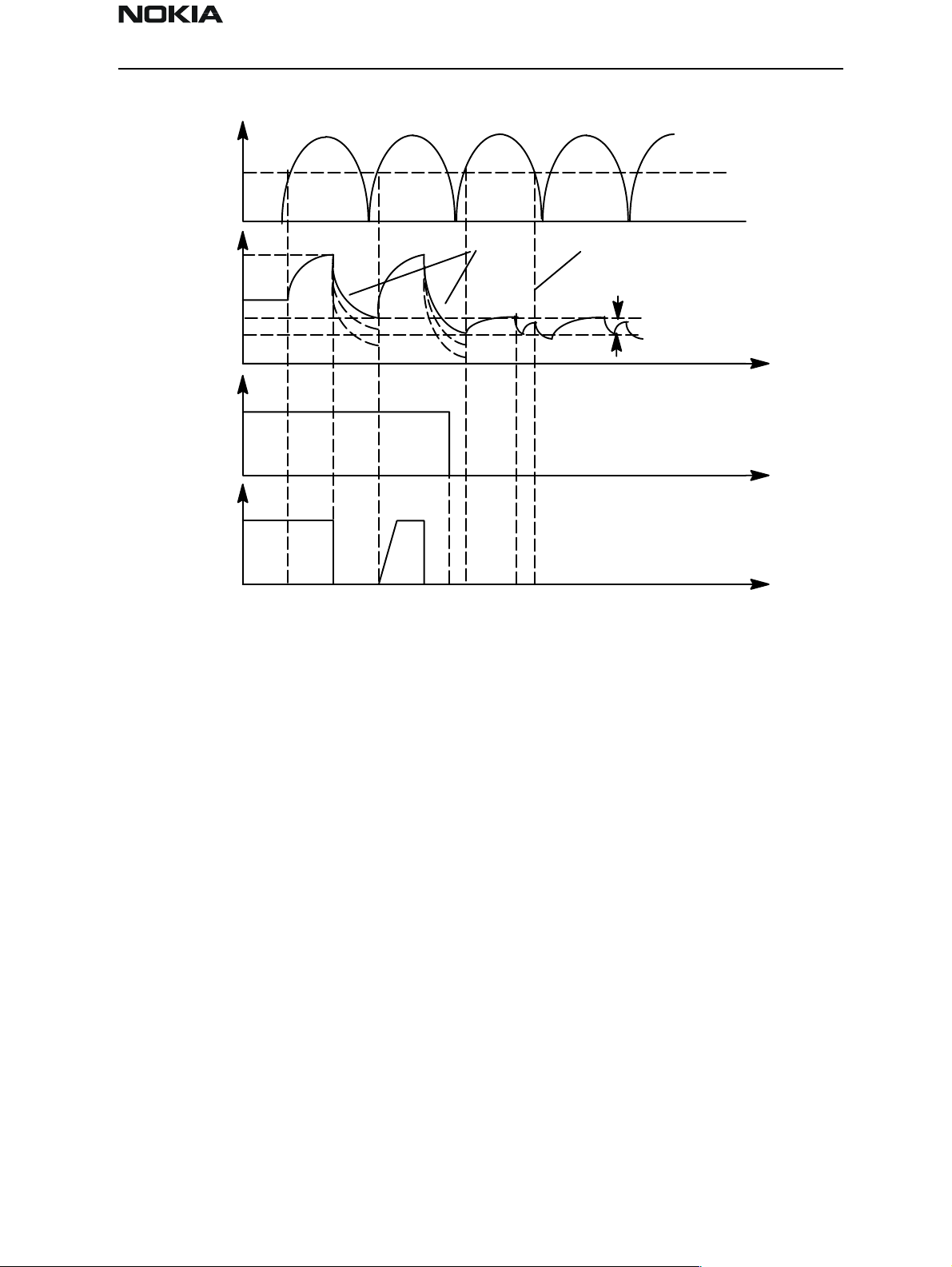
Battery Removal During Cha r g i n g
Output overvoltage protection is also needed in case the main battery is removed when
charger connected or charger is connected before the battery is connected to the phone.
With a charger connected, if VOUT exceeds VLIM1 (or VLIM2), CHAPS turns switch OFF
until the charger input has sunken below Vpor (nominal 3.0V, maximum 3.4V). MCU software will stop the charging (turn off PWM) when it detects that battery has been
removed. The CHAPS remains in protection state as long as PWM stays HIGH after the
output overvoltage situation has occurred.
ON
Page 26 Nokia Mobile Phones Ltd. Issue 1 03/01
Page 27
NSB-5
PAMS Technical Documentation System Module
VCH
(Standard
Charger)
VOUT
PWM
SWITCH
Vpor
VLIM
4V
Vstart
”1”
”0”
ON
OFF
Droop depends on load
& C in phone
2134
Istart off due to VCH<Vpor
Vstarthys
t
t
5
67
t
1 Battery removed, (standard) charger connected, VOUT rises (follows charger volt-
age)
2 VOUT exceeds limit VLIM(X), switch is turned immediately OFF
3 VOUT falls (because no battery), also VCH<Vpor (standard chargers full–rectified
output). When VCH > Vpor and VOUT < VLIM(X) –> switch turned on again (also
PWM is still HIGH) and VOUT again exceeds VLIM(X).
4 Software sets PWM = LOW –> CHAPS does not enter PWM mode
5 PWM low –> Startup mode, startup current flows until Vstart limit reached
6 VOUT exceeds limit Vstart, Istart is turned off
7 VCH falls below Vpor
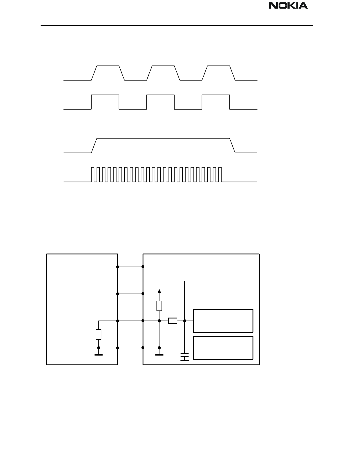
Different PWM Frequencies (1Hz and 32 Hz)
When a travel charger (2–wire charger ) is used, the power switch is turned ON and OFF
by the PWM input when the PWM rate is 1Hz. When PWM is HIGH, the switch is ON and
the output current Iout = charger current – CHAPS supply current. When PWM is LOW,
the switch is OFF and the output current Iout = 0. To prevent the switching transients
inducing noise in audio circuitry of the phone soft switching is used.
Issue 1 03/01 Nokia Mobile Phones Ltd. Page 27
Page 28
NSB-5
System Module PAMS Technical Documentation
The performance travel charger (3– wire charger) is controlled with PWM at a frequency
of 32Hz. When the PWM rate is 32Hz CHAPS keeps the power switch continuously in the
ON state.
SWITCH
PWM (1Hz)
SWITCH
PWM (32Hz)
Battery Identification
Different battery types are identified by a pulldown resistor inside the battery pack. The
BSI line inside transceiver has a 100k pullup to VBB.
The MCU can identify the battery by reading the BSI line DC–voltage level with a CCONT
(N100) A/D–converter.
ON ONON OFF OFF
ON
BVOLT
BATTERY
BTEMP
BSI
R
s
BGND
Figure 10: Battery Identification
Vbb
Vibra Schematic
100k
10k
10n
BSI
SIMCardDetX
TRANSCEIVER
CCONT
MAD
The battery identification line is used also for battery removal detection. The BSI line is
connected to a SIMCardDetX line of MAD2 (D300). SIMCardDetX is a threshold detector
with a nominal input switching level 0.85xVcc for a rising edge and 0.55xVcc for a falling
edge. The battery removal detection is used as a trigger to power down the SIM card
before the power is lost. The BSI contact in the battery pack is made 0.7mm shorter than
the supply voltage contacts so that there is a delay between battery removal detection
Page 28 Nokia Mobile Phones Ltd. Issue 1 03/01
Page 29
NSB-5
PAMS Technical Documentation System Module
and supply power off.
Vcc
0.850.05 Vcc
0.550.05 Vcc
SIMCARDDETX
S
GND
IGOUT
Battery Temperature
The battery temperature is measured with a NTC inside the battery pack. The BTEMP line
inside transceiver has a 100k pullup to VREF. The MCU can calculate the battery temperature by reading the BTEMP line DC–voltage level with a CCONT (N100) A/D–converter.
BVOLT
BATTERY
NTC
Supply Voltage Regulators
The heart of the power distrubution is the CCONT. It includes all the voltage regulators
and feeds the power to the whole system. The baseband digital parts are powered from
the VBB regulator which provides 2.8V baseband supply. The baseband regulator is active
always when the phone is powered on. The VBB baseband regulator feeds M AD and
memories, COBBA digital parts and the LCD driv er in the UI section. There is a separate
regulator for a SIM card. The regulator is selectable between 3V and 5V and controlled by
the SIMPwr line from MAD to CCONT. The COBBA analog parts are powered from a dedicated 2.8V supply VCOBBA. The CCONT also supplies 5V for RF. The CC ONT contains a real
time clock function, which is powered from a RTC backup when the main battery is disconnected.
TRANSCEIVER
BSI
BTEMP
R
T
BGND
1k
VREF
100k
2k2
10k
10n
BTEMP
VibraPWM
MCUGenIO4
CCONT
MAD
Figure 11: Battery Temperature
The RTC backup is rechargable polyacene battery, which has a capacity of 50uAh (@3V/
2V) The battery is charged from the main battery v o ltage by the CHAPS when the main
battery voltage is over 3.2V. The charging current is 200uA (nominal).
Issue 1 03/01 Nokia Mobile Phones Ltd. Page 29
Page 30
NSB-5
System Module PAMS Technical Documentation
Table 8: Regulator States for Different Modes of Oper atio n
Operating mode Vref RF REG VCOBBA VBB VSIM SIMIF
Pow er o ff
Pow er o n
Reset
Sleep
Off
On
On
Off
Note: CCONT includes five additional 2.8V regulators providing power to the RF section. These regulators can be controlled either by the direct control signals from MAD or by the RF r egulator control
register in CCONT which MAD can update. Below are the listed the MAD control lines and the regulators they control:
- TxPwr controls VTX regulator (VR7)
- RxPwr controls VRX regulators (VR2 and VR5)
- SynthPwr controls VSYN_1 and VSYN_2 regulators (VR1_SW and VR4)
VCXOPwr controls VXO regulator (VR1)
Off Off Off Off Pull down
On/Off On On On On/off
Off
VR1 On
Off Off On On On/off
On On On Pull down
CCONT generates also a 1.5 V reference voltage VREF to COBBA, SUMMA, and CRFU. The
VREF voltage is also used as a reference to some of the CCONT A/D converters.
In addition to the above-mentioned signals, MAD includes TXP control signal, which goes
to SUMMA power control block and to the power amplifier. The transmitter power control TXC is led from COBBA to SUMMA.
Audio Control
The audio control and processing is handled by the COBBA–GJP, which contains the
audio and RF codecs, and the MAD2, which contains the MCU, ASIC, and DSP blocks
handling and processing the audio signals.
Page 30 Nokia Mobile Phones Ltd. Issue 1 03/01
Page 31

NSB-5
PAMS Technical Documentation System Module
Slide
System
EMI
Connect or
Display
XMIC
SGND
XEAR
EMI
Bias +
EMI+ACC
Interf.
EMI
AuxOut
MIC2
MIC1
MIC3
HF
EAR
Preamp
Amp
Multipl.Premult.
Multipl.
COBBA
Pre
& LP
LP
A
D
D
A
DSP
MAD
MCU
Buzzer
Driver
Circuit
Buzzer
Figure 12: Audio Control
The baseband supports three microphone inputs and two earphone outputs. The inputs
can be taken from an internal microphone, a headset mic rophone or from an external
microphone signal source. The microphone signals from different sources are connected
to separate inputs at the COBBA–GJP asic. Inputs for the microphone signals are differential type.
The MIC1 inputs are used for a headset microphone that can be connected directly to the
system connector. The internal microphone is connected to MIC2 inputs and an external
pre–amplified microphone (handset/handfree) signal is connected to the MIC3 inputs. In
COBBA there are also three audio signal outputs of which dual ended EAR lines are used
for internal earpiece and HF line for accessory audio output. The third audio output AUXOUT is used only for bias supply to the headset microphone. As a difference to DCT2 generation the SGND does not supply audio signal (only common mode). Therefore there are
no electrical loopback echo from downlink to uplink.
The output for the internal earphone is a dual ended type output capable of driving a
dynamic type speaker. The output for the external accessory and the headset is single
ended with a dedicated signal ground SGND. Input and output signal source selection
and gain control is performed inside the COBBA–GJP asic according to control messages
from the MAD2. Keypad tones, DTMF, and other audio tones are generated and encoded
by the MAD2 and transmitted to the COBBA–GJP for decoding.
Internal Microphone and Earpiece
The baseband supports three microphone inputs and two earphone outputs. The inputs
can be taken from an internal microphone, a headset mic rophone, or from an external
microphone signal source. The microphone signals from different sources are connected
to separate inputs to the COBBA_GJP asic. Inputs for the microphone signals are of a differential type.
Issue 1 03/01 Nokia Mobile Phones Ltd. Page 31
Page 32

NSB-5
System Module PAMS Technical Documentation
External Audio Connections
The external audio connections are presented in figure 16. A headset can be connected
directly to the system connector. The headset microphone bias is supplied from COBBA
AUXOUT output and fed to microphone through XMIC line. The 330ohm resistor from
SGND line to AGNDprovides a return path for the bias current.
Baseband
HOOKDET
MAD
HEADDET
CCONT
COBBA–
GJP
AUXOUT
EAD
H
F
PD2
10m
AGND
10k
100n
AGND
27p
10u
100n
1u
220k
220k
VBB VBB
2k2 47k
2k2
VBB
33R
100MHz
47k
47R
AGND
XEAR
LGN
D
R01
SW01
PC–Board
C01
+
+
+
C03
C02
HFC
M
MIC1
N
MIC1
P
MIC3
N
MIC3
P
100n
100n
100n
100n
AGND
AGND
27p
AGND AGND AGND
Figure 13: Combined headset and system connector audio signal
Analog Audio Accessory Detection
In XEAR signal there is a 47 kΩ pullup in the transceiver and 6.8 kΩ pull–down to SGND
in accessory. The XEAR is pulled down when an accessory is connected, and pulled up
when disconnected. The XEAR is connected to the HookDet line (in MAD), an interrupt is
given due to both connection and disconnection. There is filtering between XEAR and
HookDet to prevent audio signal giving unwanted interrupts.
2k2
27p
2k2
330R
100R
100R
XMI
C
SGN
D
L01
R01= 100R
C01=33uF
C02=1000pF
C03=22pF
L01=MMZ2012Y6
01BT/TDK
Z01
Page 32 Nokia Mobile Phones Ltd. Issue 1 03/01
Page 33

NSB-5
PAMS Technical Documentation System Module
External accessory notices powered–up phone by detecting voltage in XMIC line. In
Table 9 there is a truth table for detection signals.
Table 9: HookDet/HeadDet Detection Truth Table
Accessory connected HookDet HeadDet Notes
No accessory connected High HIgh Pull-ups in the transceiver
Headset HDC-9 with a button
switch pressed
Headset HDC-9 with a button
switch released
Handsfree (HFU-1) Low High XEAR loaded (dc)
Low Low XEAR and XMIC loaded (dc)
High Low *) XEAR unloaded (dc)
Internal Audio Connections
The speech coding functions are performed by the DSP in the MAD2 and the coded
speech blocks are transferred to the COBBA–GJP for digital to analog conversion, down
link direction. In the up link direction the PCM coded speech blocks are read from the
COBBA–GJP by the DSP.
There are two separate interfaces between MAD2 and COBBA–GJP: a parallel bus and a
serial bus. The parallel bus has 12 data bits, 4 address bits, read and write strobes, and a
data available strobe. The parallel interface is used to transfer all the COBBA–GJP control
information (both the RFI part and the audio part) and the transmit and receive samples.
The serial interface between MAD2 and COBBA–GJP includes transmit and receive data,
clock and frame synchronization signals. It is used to transfer the PCM samples. The
frame synchronization frequency is 8 kHz which indicates the rate of the PCM samples
and the clock frequency is 1 MHz. COBBA is generating both cloc ks.
4–wire PCM Serial Interface
The interface consists of following signals: a PCM codec master clock (PCMDClk), a
frame synchronization signal to DSP (PCMSClk), a codec transmit data line (PCMTX), and
a codec receive data line (PCMRX). The COBBA–GJP generates the PCMDClk clock, which
is supplied to DSP SIO. The COBBA–GJP also generates the PCMSClk signal to DSP by
dividing the PCMDClk. The PCMDClk frequency is 1.000 MHz and is generated by dividing
the RFIClk 13 MHz by 13. The COBBA–GJP further divides the PCMDClk by 125 to get a
PCMSClk signal, 8.0 kHz.
PCMDClk
PCMSClk
PCMTxData
PCMRxData
sign extended
15 14 13 12 011 10
sign extended
MSB
MSB
LSB
LSB
Issue 1 03/01 Nokia Mobile Phones Ltd. Page 33
Page 34

NSB-5
System Module PAMS Technical Documentation
The output for the internal earphone is a dual ended type output capable of driving a
dynamic type speaker. The output for the external accessory and the headset is single
ended with a dedicated signal ground SGND. Input and output signal source selection
and gain control is performed inside the COBBA_GJP asic according to control messages
from the MAD2WD1. Keypad tones, DTMF, and other audio tones are generated and
encoded by the MAD2WD1 and transmitted to the COBBA_GJP for decoding. MAD2WD1
generates two separate PWM outputs, one for a buzzer and one for vibra (internal and
external via BTEMP).
Speech Processing
The speech coding functions are performed by the DSP in the MAD2WD1 and the coded
speech blocks are transferred to the COBBA_GJP for digital to analog conversion, down
link direction. In the up link direction the PCM coded speech blocks are read from the
COBBA_GJP by the DSP.
There are two options for the PCM interface between MAD 2WD1 and COBBA_GJP. The
4-pin solution and a 1-pin solution. The four pin serial interface between MAD2WD1 and
COBBA_GJP includes transmit and receive data, clock and frame synchronization signals.
It is used to transfer the PCM samples. The frame synchronization frequency is 8 kHz,
which indicates the rate of the PCM samples and the clock frequency is 1 MHz.
COBBA_GJP generates both clocks. NSB–5 uses the 4–pin solution.
Alert Signal Generation
A buzzer is used for giving alerting tones and/or melodies as a signal of an incoming call.
Also keypress and user function response beeps are generated with the buzzer. The
buzzer is controlled with a BuzzerPWM output signal from the MAD2WD1. A dyna mic
type of buzzer is used since the supply voltage available cannot produce the required
sound pressure for a piezo type buzzer. The low impedance buzzer is connected to an
output transistor that gets drive current from the PWM output. The alert volume can be
adjusted either by changing the pulse width causing the level to change or by changing
the frequency to utilize the resonance frequenc y range of the buzzer.
Digital Control
MAD2WD1
The baseband functions are controlled by the MAD2WD1 ASIC, which consists of a MCU,
a system ASIC, and a DSP. The GSM/PCN-specific ASIC is named MAD2. There are separate controller ASICs in TDMA and JDC named MAD1 and MAD3. All the MAD2WD1
ASICs contain the same core processors and similar building blocks, but differ from each
other in system specific functions, pinout, and package types.
• MAD2WD1 contains following building blocks:
• ARM RISC processor with both 16–bit instruction set (THUMB
mode) and 32–bit instruction set (ARM mode)
• TMS320C542 DSP co re with peripherials:
– API (Arm Port Interface memory) for MCU–DSP communication,
Page 34 Nokia Mobile Phones Ltd. Issue 1 03/01
Page 35

NSB-5
PAMS Technical Documentation System Module
DSP code download, M CU in terr upt ha ndling vector s (in DS P RAM)
and DSP booting
– Serial port (connection to PCM)
– Timer
– DSP memory
• BUSC (BusController for controlling accesses from ARM to API,
System Logic, and MCU external memories, both 8– and 16–bit
memories)
• System Logic
– CTSI (Clock, Timing, Sleep and Interrupt control)
– MCUIF (Interface to ARM via BUSC). Contains MCU BootROM
– DSPIF (Interface to DSP)
– MFI (Interface to COBBA_GJP AD/DA Converters)
– CODER (Block encoding/decoding and A51&A52 ciphering)
– AccIF (Accessory Interface)
– SCU (Synthesizer Control Unit for contro lling 2 separate synthesizer)
– UIF (Keyboard interface, serial control interf ace for COBBA_
GJP PCM Codec, LCD Driver, and CCONT)
– UIF+ (roller/ sl ide handling)
– SIMI (SimCard interface with enhanched features)
– PUP (Parallel IO, USART and PWM control unit for vibra and
buzzer)
– FLEXPOOL (DAS00308 FlexPool Specification)
– SERRFI (DAS00348 COBBA_GJP Specifications)
The MAD2WD1 operates from a 13 MHz system clock, which is generated from the
13Mhz VCXO frequency. The MAD2WD1 supplies a 6.5MHz or a 13MHz internal clock for
the MCU and system logic blocks and a 13MHz clock for the DSP, where it is multiplied
to 78 MHz DSP clock. The system clock can be stopped for a system sleep mode by disabling the VCXO supply power from the CCONT regulator output. The CCONT provides a
32kHz sleep clock for internal use and to the MAD2WD1, which is used for the sleep
mode timing. The sleep clock is active when there is a battery voltage available; i.e.,
always when the battery is connected.
MAD2WD1 pinout
MAD2WD1 pins and their usage are described in the following table.
Ball
No.
A1 MCUGenIO0 I/O 2 MCU general purpose I/O DLR-3 (data cable)
B1 SynthClk O 2 Synth clk control bit to
Pin Name Pin Type
Table 10: MAD2WD1 pin list
Drive /
pull
Description HD955 Function
power cont rol bit
SUMMA
Issue 1 03/01 Nokia Mobile Phones Ltd. Page 35
Page 36

NSB-5
System Module PAMS Technical Documentation
C1 DSPGenOut2 I/O 2 DSP general purpose port TXL to RF
D1 LCDCSX I/O 2 Serial LCD chip select –
external pull-up/down
E1 LEADVCC0 PWR LEAD power Supply = VBB
F1 Row0 I/O 2/up Keyboard row0, parallel
LCD driver data
G1 VCC_CORE PWR Power supply for core Supply = V2V
H1 VCC_IO PWR I/O power supply Supply = VBB
J1 MCUAd16 O 2 MCU address bus SRAM/FLASH address 16
K1 MCUAd13 I/O 2 MCU address bus SRAM/FLASH address 13
L1 ARMGND ARM GND GND
M1 MCUAd6 I/O 2 MCU address bus SRAM/FLASH address 6
N1 MCUAd2 I/O 2 MCU address bus SRAM/FLASH address 2
A2 TxPA I/O 2/down Power amplifier control TXP to RF
B2 SynthData O 2 Synthesizer data SDATA to SUMMA
C2 LEADGND LEAD gnd GND
D2 Col4 I/O 2/up Keyboard column 4 – pro-
grammable pull-up
LCDEN
Keyboard row0
Keyboard col4
E2 Row4 I/O 2/up Keyboard row 4, parallel
LCD dirver register selec-
tion control
F2 Row1 I/O 2/up Keyboard row 3, parallel
LCD driver data
G2 MCUAd21 I/O 2/up MCU address bus FLASH address 21
H2 MCUAd18 O 2 MCU address bus SRAM/FLASH address 18
J2 MCUAd15 I/O 2 MCU address bus SRAM/FLASH address 15
K2 MCUAd12 I/O 2 MCU address bus SRAM/FLASH address 12
L2 MCUAd9 I/O 2 MCU address bus SRAM/FLASH address 9
M2 MCUAd8 I/O 2 MCU address bus SRAM/FLASH address 8
N2 MCUAd1 I/O 2 MCU address bus SRAM/FLASH address 1
A3 FrACtrl I/O 2/down RF front amplifier control LNA_AGC
B3 SynthEna1X O 2 Synthesizer1 data enable Synth enable (SUMMA)
C3 Col0 I/O 2/up Keyboard column 0 Keyboard column 0
D3 Col3 I/O 2/up Keyboard column 3 Keyboard column 3
Keyboard row4
Keyboard row1
Page 36 Nokia Mobile Phones Ltd. Issue 1 03/01
Page 37

NSB-5
PAMS Technical Documentation System Module
E3 Row5LCDCD I/O 2/up Keyboard row5 data I/O,
serial LCD driver command/
data indicator, parallel LCD
driver read/write select
F3 Row2 I/O 2/up Keyboard row2, parallel
LCD driver data
G3 MCUAd20 I/O 2/down MCU address bus SRAM/FLASH address 20
H3 MCUAd17 O 2 MCU address bus SRAM/FLASH address 17
J3 MCUAd14 I/O 2 MCU address bus SRAM/FLASH address 14
K3 MCUAd11 I/O 2 MCU address bus SRAM/FLASH address 11
L3 MCUAd8 I/O 2 MCU address bus SRAM/FLASH address 8
M3 MCUAd4 I/O 2 MCU address bus SRAM/FLASH address 4
N3 MCUAd0 O 2 MCU address bus SRAM address 0
A4 DSPGenOut4 I/O 2 DSP general purpose port IRON – Enable control
B4 SynthEna2X I/O 2 Synthesizer 2 data enable NC
C4 Col1 I/O 2/up Keyboard column 1 Keyboard column 1
LCDCD (LCD driver command/data indicator)
Keyboard row2
for IrDa
D4 Col2 I/O 2/up Keyboard column 2 Keyboard column 2
E4 GND GND Ground GND
F4 Row3 I/O 2/up Keyboard row3, parallel
LCD driver data
G4 MCUAd19 O 2 MCU address bus SRAM/FLASH address 19
H4 LEADGND GND LEAD ground GND
J4 GND GND Ground GND
K4 ARMVCC PWR ARM power VBB
L4 MCUAd7 I/O 2 MCU address bus SRAM/FLASH address 7
M4 MCUAd3 I/O 2 MCU address bus SRAM/FLASH address 3
N4 VCC_CORE PWR Core power Core power – supplied
A5 DSPGenOut5 O 2 DSP general purpose out-
put, COB BA reset
B5 MBUS I/O 2/up MBUS, Flash clock – exter-
nal pull-up
C5 AccTxData O 2 Accessory Tx data, Flash_Tx
– external pull-up
Keyboard row3
from CCONT V2V
COBBA reset
MBUS, Flash clock
Accessory Tx data,
Flash_Tx (FBUS_Tx)
D5 GND GND Ground GND
K5 MCUAd10 O 2 MCU address bus SRAM/FLASH address 10
L5 GND GND Ground GND
Issue 1 03/01 Nokia Mobile Phones Ltd. Page 37
Page 38

NSB-5
System Module PAMS Technical Documentation
M5 MCURdX O 2 MCU read strobe MCU read strobe – OE
to memories
N5 MCUWrX O 2 MCU write strobe MCU write strobe – WE
to memories
A6 COBBACSX O 2 Chip select for COBBA CO BBA chip select
B6 VCC_IO PWR I/O power VBB
C6 COBBAClk O 4 COBBA clock, 13MHz COBBA clk (RFIclk)
D6 AccRxData I Accessory Rx data,
Flash_Rx
K6 ExtMCUDa0 I/O 2/down MCU data bus SRAM/FLASH data 0
L6 ExtMCUDa1 I/O 2/down MCU data bus SRAM/FLASH data 1
M6 ExtMCUDa2 I/O 2/down MCU data bus SRAM/FLASH data 2
N6 ExtMCUDa3 I/O 2/down MCU data bus SRAM/FLASH data 3
A7 COBBASDa I/O 2 Transfer of control data Transfer of control data
B7 VCC_CORE PWR Core power Core power – supplied
C7 COBBAIDa I/O 2 Bidirectional transfer of in-
phase samples
D7 COBBAQDa I/O 2 Bidirectional transfer of
quadrature samples
K7 VCC_IO PWR I/O power VBB
L7 ExtMCUDa4 I/O 2/down MCU data bus SRAM/FLASH data 4
Accessory Rx data,
Flash_Rx (FBUS_Rx)
(COBBA SD)
from CCONT V2V
Bidirectional transfer of
in-phase samples
(COBBA Idata)
Bidirectional transfer of
quadrature samples
(COBBA Qdata)
M7 ExtMCUDa5 I/O 2/down MCU data bus SRAM/FLASH data 5
N7 ExtMCUDa6 I/O 2/down MCU data bus SRAM/FLASH data 6
A8 PCMSClk I/O Down Transmit frame sync, FSX Transmit frame sync,
FSX (to COBBA)
B8 PCMDClk I/O Down Transmit clock, CLKX Transmit clock, CLKX (to
COBBA)
C8 PCMIO I/O ROLLER_A – Input bit
for roller
D8 DSPXF I/O 2/up E x te rn al flag External flag – NC
K8 MCUGenIODa2 I/O 2/down General purpose I/O port –
MCU data in 16-bit mode
L8 MCUGenIODa1 I/O 2/down Gener al purpose I/O port –
MCU data in 16-bit mode
M8 MCUGenIODa0 I/O 2/down G eneral purpose I/O port –
MCU data in 16-bit mode
FLASH data 10
FLASH data 9
FLASH data 8
Page 38 Nokia Mobile Phones Ltd. Issue 1 03/01
Page 39

NSB-5
PAMS Technical Documentation System Module
N8 ExtMCUDa7 I/O 2/down MCU data bus SRAM/FLASH data 7
A9 PCMRxData I/O Up Receive data, Rx Receive data, Rx (from
COBBA PCMTx)
B9 PCMTxData I/O 2/down Transmit data, Tx Transmit data, Tx (to
COBBA PCMRx)
C9 GND GND Ground GND
D9 BuzzPWM I/O 2/down Buzzer PWM control Buzzer PWM control
K9 GND I/O Ground GND
L9 MCUGenIODa5 I/O 2/down Gener al purpose I/O port –
MCU data in 16-bit mode
M9 MCUGenIODa4 I/O 2/down G eneral purpose I/O port –
MCU data in 16-bit mode
N9 MCUGenIODa3 I/O 2/down General purpose I/O port –
MCU data in 16-bit mode
A10 GenSClk O 2 Serial clock Serial clock (to LCD)
B10 GenSDIO I/O 2 Serial data in/out – exter-
nal pull-up/down depend-
ing on how to boot
C10 GenCCONTCSX O 2 C h ip select to CCONT Chip select to CCONT
D10 VCC_IO PWR I/O Power I/O Power (VBB)
E10 GND GND Ground GND
F10 HeadDet I/O Headset detection inter-
rupt
G10 MCUGenIO4 I/O 2 MCU data in 16-bit mode
pullup
H10 LEADVCC PWR LEAD power LEAD pwr (VBB)
FLASH data 13
FLASH data 12
FLASH data 11
Serial data in/out (to
LCD)
Headset detection interrupt (to CCONT EAD)
BATTIO through BTEMP
J10 SCGND GND Special cell ground GND
K10 SCVCC PWR Special cell power VBB
L10 MCUGenIODa7 I/O 2/down General purpose I/O port –
MCU data in 16-bit mode
M10 VCC_CORE PWR Core power Core power – supplied
N10 MCUGenIODa6 I/O 2/down General purpose I/O port –
MCU data in 16-bit mode
A11 SIMCardIOC O 2 SIM data in/out control SIM data in/out control
B11 SIMCardRstX O 2 SIM reset SIM reset (to CCONT)
C11 SIMCardData I/O 2 SIM data SIM data (to CCONT)
D11 LEADVCC PWR LEAD power LEAD pwr (VBB)
FLASH data 15
from CCONT V2V
FLASH data 14
(to CCONT)
Issue 1 03/01 Nokia Mobile Phones Ltd. Page 39
Page 40

NSB-5
System Module PAMS Technical Documentation
E11 VCXOPwr O 2 VCXO regulator control Sleep control (to CCONT
SLEEPX input)
F11 HookDet I/O Non-MBUS accessory con-
nection detector
G11 VCC_CORE PWR Core power Core power – supplied
H11 MCUGenIO1 I/O 2/up General purpose I/O port FLASH write protect
J11 ROM2SelX I/O 2/up Extra chip select, can be
used as MCU general out-
put
K11 RFClk I System clock from VCTCXO System clock from
L11 JTDO I/O 2/up JTAG data out JTAG data out
M11 RAMSelX O 2 RAM chip select RAM chip select
N11 ROM1SelX O 2 ROM chip select Enable for 4M FLASH
A12 SIMCardClk O 2 SIM clock SIM cl ock (to CCONT)
B12 CCONTInt I CCONT interrupt CCONT interrupt
C12 TxPwr I/O 2/down Tx regulat or c o nt rol Tx regulator control (to
Non-MBUS accessory
connection detector
(system conn. XEAR)
from CCONT V2V
Enable for 2M FLASH
chip
VCTCXO
chip
CCONT)
D12 SIMCardPwr I/O 2/up SIM power control S IM power co ntrol (to
CCONT)
E12 MCUGenIO3 I/O 2/up General purpose I/O port VPP supply for FLASH
F12 LoByteSelX I/O 2/up ROLLER_B – Input bit
for roller
G12 VibraPWM I/O 2/down Vibra PWM control Vibra PWM control
H12 TestMode I Down Test mode select Test mode select (GND)
J12 GND GND Ground GND
K12 RFClkGnd I System clock reference
ground input
L12 CoEmu0 I/O 2/up DSP/MCU emulation port 0 DSP/MCU emulation
M12 JTClk I/O Up JTAG clock JTAG clock
N12 JTRst I/O Down JTAG res et JTAG reset
A13 Clk32k I Sleep clock oscillator input Sleep clo ck oscillator
B13 PURX I Power-up reset Power-up reset (from
System clock refer e nc e
ground input (GND)
port 0 – JTAG
input
CCONT)
Page 40 Nokia Mobile Phones Ltd. Issue 1 03/01
Page 41

NSB-5
PAMS Technical Documentation System Module
C13 RxPwr I/O 2/down Rx regulator control Base tune enable/disa-
ble control
D13 SynthPwr I/O 2/down Synthesizer regulator con-
trol
E13 MCUGenIO2 I/O 2/up General purpose I/O port LCDRSTX – LCD reset
F13 LEADGND GND LEAD ground GND
G13 VCC_IO PWR VCC power VBB
H13 ExtSysResetX O 2 System reset FLASH read protect co n-
J13 EEPROMSelX I/O 2/up EEPROM chip select, can
be used as MCU gernal
output
K13 SIMCardDetX I SIM card d et e ct ion SIM card detection (to
L13 CoEmu1 I/O 2/up DSP/MCU emulation port 1 DSP/MCU emulation
M13 JTMS I/O Up JTAG mode select JTAG mode select
N13 JTDI I/O Up JTAG data in JTAG data in
Transmit power control
enable
control
trol
ROLLER_C – i nput bit
for roller
CCONT BSI input)
port 1
Table 11: COBBA_GJP pin li st
Ball
No.
A1 MIC1P I - Positive high impedance input for
B1 MIC3N I - Third negative high impedance
C1 VSUBA P Analog Substrate contact for RF
D1 EARP O Float Positive ear-piece output To internal speaker
E1 HF O Float Output for phone external audio
F1 VDA2 P - Positive analog power supply for
G1 IREF O float Reference current output (no
H1 VSA2 P - Negative analog power supply for
Name Type
Reset
Value
Description HD955 Function/Connection
Analog input from external
microphone
input for microphone
analog and AudioCodec
circuitry
the transmitters
capacitance allowed on this pin)
the tranmitters
microphone
Analog input from external
microphone
AGND
To system connector for external analog audio
VCOBBA from CCONT
Through 100k to AGND
AGND
A2 MIC1N I Inp Negative high impedance input
for microphone
B2 MIC3P I - Third positive high impedance
input for microphone
Analog input from external
microphone
Analog input from external
microphone
Issue 1 03/01 Nokia Mobile Phones Ltd. Page 41
Page 42

NSB-5
System Module PAMS Technical Documentation
C2 VSA5 P - Negative analog power supply for
PCM ADC
D2 EARN O Float Negative ear-piece output To internal speaker
E2 VSA4 P - Negative analog power supply for
PCM DAC
F2 VREF I - Reference voltage input (1.5V) VREF from CCONT
G2 AFCOut O Float Automatic frequency control o ut-
put
H2 TxIOutN O Float Negative in-phase transmit out-
put
A3 MIC2N I Inp Second negative high impedance
input for microphone
B3 MIC2P I Inp Second positive high impedance
input for microphone
C3 VDA5 P _ Positive analog power supply for
PCM ADC
D3 HFCM O Float Common mode output for phone
external audio circuitry
AGND
AGND
To 13MHz clock oscillator
To SUMMA
Analog input from slide microphone
Analog input from slide microphone
VCOBBA from CCONT
Not used (floating)
E3 VDA4 P - Positive analog power supply for
PCM DAC
F3 TxQOutP O Float Positive quadrature transmit out-
put
G3 TxQOutN O Float Negative quadrature transmit
output
H3 TxIOutP O Float Positive in-phase transmit output To SUMMA
A4 MBIAS O Float Bias output for microphone 2.1V Bias output for microphone
B4 VDD1 P - AudioCodec positive digital
power supply
C4 VSS1 P - AudioCodec negative digital
power supply
D4 AUXOUT O Float Auxiliary audio output or ABIAS
2.1V
E4 VDA3 P - Positive analog power supply VCOBBA from CCONT
F4 TxCOut O Float Transmit power control output Transmit power control output
VCOBBA from CCONT
To SUMMA
To SUMMA
2.1V
VBB
GND
Auxiliary audio output or ABIAS
2.1V
– to SUMMA
G4 TxIPhsP O Float Positive in-phase PHS transmit
output
H4 TxIPhsN O Float Negative in-phase PHS transmit
output
A5 TEST I Inp Te st pin GND
Not used (floating)
Not used (floating)
Page 42 Nokia Mobile Phones Ltd. Issue 1 03/01
Page 43

NSB-5
PAMS Technical Documentation System Module
B5 PCMTx I/O ‘Z’ PCM bus receive data (4-wire) / I/
O data (1-wire)
C5 PCMSCLK O ‘Z’ 8 kHz frame sync (4-wire) /
Pdata(8) (1-wire)
D5 PCMRx I/O ‘Z” PCM bus receive data (4-wire) /
Pdata(10) (1-wire)
E5 Pdata(0) O ‘0’ Pdata(0) / Scanselect when
test=1
F5 AGCOut O 0V Second output of TxC DAC – Rx
gain control voltage
G5 TxQPhsP O Float Positive quadrature PHS transmit
output
H5 TxQPhsN O Float Negative quadrature PHS trans-
mit output
A6 Idata I/O Inp Bi-directional transfer of I-sam-
ples / Pdata(5) when JDC+IQ=0
and DuplexIQ=0 and JDC mode
B6 Qdata I/O Imp Bi-directional transfer of Q-sam-
ples / Pdata(6) when JDC+IQ=0
and DuplexIQ=0 and JDC mode
To MAD2WD1 PCMRxData
To MAD2WD1 PCMSClk
To MAD2WD1 PCMTxData
Not used (floating)
To SUMMA
Not used (floating)
Not used (floating)
To MAD2WD1 COBBAIda
To MAD2WD1 COBBAQda
C6 PCMDCLK O ‘Z’ PCM bus data transfer clock (4-
wire) / Pdata(9) (1-wire) – 520
kHz
D6 Pdata(3) O ‘0’ Pdata(3) / RxI data in DuplexIQ
mode
E6 Pdata(1) O ‘0’ Pdata(1) / Capture/shift when
test=1
F6 VSA1 P - Negative analog power supply for
receivers
G6 AuxDAC O 0V Third output of TxC DAC Not used (floating)
H6 VSA3 P - Negative analog power supply AGND
A7 SD I/O Inp Serial data for the general inter-
face
B7 CSX I Inp Serial port chip select To MAD2WD1 COBBACSX
C7 PData(4) O ‘0’ Pdata(4) / RxQ data in DuplexIQ
mode
D7 RFIDAX O ‘0’ Data available strobe for JDC
when JDC+IQ=0 / Pdata(7) other-
wise
To MAD2WD1 PCMDClk
LCD light (LED) driver control
Keyboard light (LED) driver control
AGND
To MAD2WD1 COBBASDa
To CHAPS VLIM (CHAPS output
voltage limit)
Not used (floating)
E7 Pdata(2) O ‘0’ Pdata(2) PD2 (Switch for 2.1V AUXOUT
bias or ABIAS)
Issue 1 03/01 Nokia Mobile Phones Ltd. Page 43
Page 44

NSB-5
System Module PAMS Technical Documentation
F7 RxQN I - Negative Q receive input in
Rx_In-phase mode
G7 VDA1 P - Positive analog power supply for
the receivers
H7 RxRef O Float Rx path internal reference buff-
ered output
A8 VSUB P - Substrate contact for digital logic GND
B8 VSS2 P - RF interface negative digital
power supply
C8 VDD2 P - RF interface positive digital
power supply
D8 RFIClk I Inp System clock input
(13 MHz)
E8 ResetX I Inp Master system reset DSPGenOut5 from MAD2WD1
F8 RxQP I - Positive Q receive input in Rx_In-
phase mode
G8 RxIP I - Positive I/common receive input From SUMMA
H8 RxIN I - Negative I/common receive input From SUMMA
AGND
VCOBBA from CCONT
Not used (floating)
GND
VBB
COBBAClk output from
MAD2WD1
AGND
Table 12: CCONT 3V pin assignment
Pin Symbol Type State in Reset Description
1 RSSI I receive signal strength indicator
2 ICHAR I V(ICHAR) voltage input
3 MODE_SEL I High Z/GND mode select High Z=normal mode
GND=RAM_Bck
4 VR3/RAM_bck O OV/2.8V VR3 regulator output/RAM backup
5 CNTVR3 I High Z Control VR3 regulator
6 CNTVR2 I High Z Control VR2 regulator
7 CNTVR5 I High Z Control VR5 regulator
8 VBAT P unregulated supply voltage (RF)
9 VR2 O High Z VR2 regulator output
10 GROUND P (RF)
11 VR5 O High Z VR5 regulator output
12 VBAT P unr e g ul ated supply voltage (RF )
13 VREF O 1.244/1.5V reference voltage output
14 GROUND P (RF)
15 VR4 O High Z VR4 regulator output
Page 44 Nokia Mobile Phones Ltd. Issue 1 03/01
Page 45

NSB-5
PAMS Technical Documentation System Module
Table 12: CCONT 3V pin assignment
Pin Symbol Type State in Reset Description
16 VBAT P unr e g ul ated supply voltage (RF )
17 CNTVR4 I High Z Control VR4 regulator
18 TXPWR I High Z Control VR7 regulator (CNTVR7)
19 VR7BASE O High Z VR7 regulator base current
20 VR7 O High Z VR7 regulator output
21 VBAT P unregulated supply voltage (RF)
22 VR6 O 2.8V VR6 regulator output (COBBA_GJ P )
23 GROUND P (RF)
24 SLEEPX I “1” Control VR1 regulator (CNTVR1)
25 VR1 O 2.8V VR1 regulator output (VCXO)
26 VR1_sw O High Z VR1 switched output
27 VBAT P unr e g ul ated supply voltage (RF )
28 VBAT2 P unregulated supply voltage (VSIM,
V5V, SMR, SIMlf)
29 PWRONX/WDDISX I VBAT/GND power on control from keyboard
watchdog disable
30 SIM_PWR I “1”/”0” SIM regulator enable
31 GROUND P (VSIM, V5V, SMR, SIMlf)
32 V5V O High Z 5V dc voltage output
33 V5V_2 O High Z reserved for 5V SMR
34 V5V_4 O High Z reserved for 5V SMR
35 V5V_3 O High Z reserved for 5V SMR
36 VSIM O 3.0V/High Z SIM regulator output
37 GROUND P (VSIM, V5V, SMR, SIMlf)
38 SIMCLK_O O “0” clock output from SIM interface
(5MHz)
39 SIM I/O_C I High Z SIM data I/O control
40 SIMRST_A I H igh Z SI M int erface reset (from
MAD2WD1)
41 SIMCLK I High Z clock to SIM interface (5MHz)
42 SIMRST_O O “0” reset output from SIM-interface
(to SIM)
43 DATA_O I/O “0” SIM data I/O line
44 DATA_A I/O “0” SIM-interface MAD2WD1 data
Issue 1 03/01 Nokia Mobile Phones Ltd. Page 45
Page 46

NSB-5
System Module PAMS Technical Documentation
Table 12: CCONT 3V pin assignment
Pin Symbol Type State in Reset Description
45 VBACK P backup battery backup battery input
46 CRA I crystal fo r 32 kHz sleep clock
47 CRB I c rys t al fo r 32 kHz sleep clock
48 SLCLK O sleep clock output
49 DATACLK I High Z MAD2WD1 bus clock
50 DATASELX I High Z MAD2WD1 bus enable
51 DATA_IN/OUT I/O High Z MAD2WD1 bus serial data
52 CCONTINT O “ 0” CC ONT i nterrupt output
53 TEST I GND t e s t p i n
(ground=>normal operation)
54 PURX O “0” power up reset signal
55 VBB O 2.8V baseband regulator output
56 PWMOUT O “0” PWM out (3/0V)
57 VBAT P unr e g ul ated supply voltage (VB B,
V2V, ADC, 32kHz)
58 GROUND P (VBB, V2V, ADC, 32kHz)
59 V2V O 1.975V MAD2WD1 core regulator output
60 VCHAR I charger voltage
61 VCXOTEMP I VCXO-temperature
62 BSI I battery type input
63 BTEMP I battery temperature input
64 EAD I external accessory detection
Memories
The MCU program code resides in an external program memory, size is 16Mbits. MCU
work (data) memory size is 1Mbits. A special block in the flash is used for storing the system and tuning parameters, user settings and selections, a scratch pad, and a short code
memory.
Separate EEPROM memories formerly used to store non-volatile data have been removed
and replaced by dedicated, write-protected blocks in flash memory. This flash solution
gives a cost and size benefit in products where large EEPROM sizes are required.
The BusController (BUSC) section in the MAD2WD1 decodes the chip select signals for
the external memory devices and the system logic. BUSC controls internal and external
bus drivers and multiplexers connected to the MCU data bus. The MCU address space is
divided into access areas with separate chip select signals. BUSC supports a programma-
Page 46 Nokia Mobile Phones Ltd. Issue 1 03/01
Page 47

NSB-5
PAMS Technical Documentation System Module
ble number of wait states for each memory range.
Program Memory 32MBit Flash
The MCU program code resides in the flash program memory.
The flash memory has a power down pin that shall be kept low, during the power up
phase of the flash to ensure that the device is powered up in the correct state (read
only). The power down pin is utilized in the system sleep mode by connecting
the VCXOPwr to the flash power down pin to minimize the flash power consumption
during the sleep.
SRAM Memory
The work memory size is 4Mbits (512kx8) static ram in a shrinked TSOP–32 package. Vcc
is 2.8V and access time is 85 ns The work memory is supplied from the common baseband VBB voltage and the memory contents are lost when the baseband voltage is
switched off. All retainable data should be stored into the flash memory when the phone
is powered down.
EEPROM Emulated in FLASH Memory
A block in flash is used for a nonvolatile data memory to store the tuning parameters and
phone setup information. The short code memory for storing user defined information is
also implemented in the flash. The flash size can vary between 2k to 8kbytes depending
on the amount of short code number locations supported. The memory is accessed
through the parallel bus.
MCU Memory Requirements
The MCU memory requirements are shown below.
Table 13: HD955 memory req u irements
Access
Product Device Organization
DCT3.5 FLASH 2Mx16 100 1 32Mbit flash chip, 2.8V rea d/w rite
DCT3.5 FLASH 1Mx16 100 1 16Mbit flash chip, 2.8V rea d/w rite
DCT3.5 SRAM 512Kx8 85 1 1 20ns @ 2.8V read/write
Time
ns
Wait
States
Used
Remarks
Flash Programming
The system connector can be used as a flash prom programming interface for flash memories for updating (i.e. re–programming) the flash program memory. Used system connector pins and their functions are listed in Table 14.
To flash the phone use service battery (BBD–3) this will automatically power up the
phone via BTEMP. When flashing, the phone has to be initialized after each file has been
flashed. The flash prommer controls the power up of the phone via the service battery.
Issue 1 03/01 Nokia Mobile Phones Ltd. Page 47
Page 48

NSB-5
System Module PAMS Technical Documentation
The program execution starts from the BOOT ROM and the MCU investigates in the early
start–up sequence if the flash prommer is connected. This is done by checking the status
of the MBUS–line. Normally this line is high, but when the flash prommer is connected,
the line is forced low by the prommer. The flash prommer serial data receive line is in
receive mode waiting for an ack nowledgement from the phone.
The data transmit line from the baseband to the prommer is initially high. When the
baseband has recognized the flash prommer, the FBUS TX–line is pulled low. This
acknowledgement is used to start the data transf er of the first two bytes from the flash
prommer to the baseband on the FBUS RX–line. The data transmission begins by starting
the serial transmission clock (MBUS–line) at the prommer.
The 2.8V programming voltage is supplied inside the transceiver from the CCONT.
For protecting the MAD2WD1 against ESD spikes at the system connector, the data
transmission lines (MBUS, RX and TX) are equipp ed with EMI filters.
Table 14: Flash programming, DC connector
Pin Name Parameter Min Typ Max Unit Remarks
1 VIN supply voltage 6.8 7.8 8. 8 V supply vo l tage
2 GND GND 0 0 V supply ground
11 MBUS ser ial clock from the prommer 2.0
0
12 FBUS_RX serial data from the prommer 2.0v
0v
13 FBUS_TX data acknowledge to the prommer 2.0
0.1
14 GND GND 0 0 V supply ground
2.8
0.8
2.8
0.8
2.8
0.8
V prommer detec-
tion and serial
clock for synchronous communication
V receive data from
prommer to baseband
Vtransmit data
from baseband to
prommer
IBI Accessories
All accessories which can be connected between the transceiver and the battery or
which itself contain the battery, are called IBI accessories.
Either the phone or the IBI accessory can turn the other on, but both possibilities are not
allowed in the same accessory.
Phone Power–on by IBI
IBI accessory can power on the phone by pulling the BTEMP line up to 3V.
Page 48 Nokia Mobile Phones Ltd. Issue 1 03/01
Page 49

NSB-5
PAMS Technical Documentation System Module
IBI power–on by phone
Phone can power the IBI accessory on by pulling the BTEMP line up by MCUGenIO4 of
MAD2. BTEMP measurement is not possible during this time.
The accessory is commanded back to power–off by MBUS message.
VB
M
Vibra
22k
100n
BATTERY
10n
R
47k
NTC
T
VBAT
BSI
BTEMP
1k
GND
Figure 14: IBI power on
VREF
100k
R214
2k2
C105
10n
10k
10k
100n
BTEMP
CCONT
VIBRAPWM
MAD
MCUGenIO4
TRANSCEIVER
3x3Ru
4k7
220k
Issue 1 03/01 Nokia Mobile Phones Ltd. Page 49
Page 50

NSB-5
System Module PAMS Technical Documentation
RF Module
RF Frequency Plan
The following figure shows the RF frequency plan used by GSM1900.
DC Characteristics
Power Distribution Diagram
Current consumption of each regulator is shown in the following power distribution diagram (Figure 16 shows maximum currents, Figure 17 shows typical currents). On the left
side of the figure, are the regulator control signals. Above each regulator is the rated
current for that regulator. The name on the right side of the regulator block (smaller
font) indicates the signal name used on the schematics. On the far right side of the figure are the pin names (power) for the different ICs.
Figure 15: RF frequency plan
Page 50 Nokia Mobile Phones Ltd. Issue 1 03/01
Page 51

NSB-5
PAMS Technical Documentation System Module
VCXOEN
RXPWR
SYNPWR
VR1
VR5
VR3
VR4
VR2
V5V
VVCXO
VRX
VSYN_D
VSYN_A
VDET
V5V
0.7mA
1.0mA
31mA
3.3mA
11mA
18mA
9.4mA
10mA
1.0mA
20mA
7.6mA
9.0mA
0.8mA
0.6mA
0.6mA
VCTCXO buffer
VCTCXO
Receiver
LNA
RX mixer UHF
VHF buffer + mix2
VHF predivider
UHF predivider
Dredividers
UHF VCO
VHF VCO
UHF buffer RX+TX
detector / temp
charge pump
charge pump
SUMMA (VRX)
CRFU2a (V_RX)
CRFU2a (V_RX)
CRFU2a (V_VHF)
SUMMA (VP1)
SUMMA (VP2)
SUMMA (VDD)
CRFU2a (V_UHF)
SUMMA (VCE1)
SUMMA (VCE2)
TXP
150mA
VR7
External
transistor
battery
VTX
VBAT
70mA
37.5mA
2.7mA
15mA
90mA
1.32 A
TX upconverter
Transmitter
Pwrcntrl opamp
TX buffer
PA gaincontrol
TX PA
CRFU2a (V_TX)
SUMMA (VTX)
SUMMA (VOP)
PA 45%
max. output
(32.5dBm)
Vbat=3.6V
Figure 16: RF power distribution: maximum currents
Issue 1 03/01 Nokia Mobile Phones Ltd. Page 51
Page 52

NSB-5
System Module PAMS Technical Documentation
VCXOEN
RXPWR
SYNPWR
VR1
VR5
VR3
VR4
VR2
V5V
VVCXO
VRX
VSYN_D
VSYN_A
VDET
V5V
0.7mA
1.0mA
31mA
3.3mA
11mA
18mA
9.4mA
10mA
1.0mA
20mA
7.6mA
9.0mA
1.6mA
0.5mA
0.5mA
VCTCXO buffer
VCTCXO
Receiver
LNA
RX mixer UHF
VHF buffer + mix2
VHF predivider
UHF predivider
Dredividers
UHF VCO
VHF VCO
UHF buffer RX+TX
detector / temp
charge pump
charge pump
SUMMA (VRX)
CRFU2a (V_RX)
CRFU2a (V_RX)
CRFU2a (V_VHF)
SUMMA (VP1)
SUMMA (VP2)
SUMMA (VDD)
CRFU2a (V_UHF)
SUMMA (VCE1)
SUMMA (VCE2)
TXP
150mA
VR7
External
transistor
battery
VTX
VBAT
49mA
33.5mA
2.4mA
14mA
70mA
1.1 A
TX upconverter
Transmitter
Pwrcntrl opamp
TX buffer
PA gaincontrol
TX PA
CRFU2a (V_TX)
SUMMA (VTX)
SUMMA (VOP)
PA 45%
max. output
(32.5dBm)
Vbat=3.6V
Figure 17: RF power distribution: typical currents
Page 52 Nokia Mobile Phones Ltd. Issue 1 03/01
Page 53

NSB-5
PAMS Technical Documentation System Module
Control Signals
Table 15: Control signals and maximum current consumption
CURRENT
VCXOEN SYNPWR RXPWR TXPWR TXP
LLLLL<10µA<10µA leakage current (PA)
H L L L L 1.7mA 3.0 mA VCTCXO active
H H L L L 42.5 mA 61.2 mA VCTCXO, VCOs PLL active
HHHLL107.8 mA143.8 mARX active
H H L H L 140 mA 186.4 mA TX active except PA
H H L H H 1310 mA 1576 mA TX active full power
consump.
(typ.)
CURRENT
consump.
(max)
Notes
Regulator Specifications
Table 16: Curren t outp u t capability/nominal voltage of RF regulators
Maxim
Regulator
VR1 to VR5 100 mA 2.8 V
um
output
current
Unit Vout Unit Notes
VR7 150 mA 2.8 V Depends on external BJT
VR7BASE -10 mA Base current limit *
V5V 30 mA 5.0 V
* default power element is PNP BJT. If a FET-device is used, special care must be taken to ensure stability.
NOTE: Maximum total current from all regulators is 330 mA rms.
Table 17: RF regulator specifications
Characteristics Condition Min Typ Max Unit
External compensation
capacitor VR1 - VR7
External compensation
capacitor VR1 - VR7
Output voltage VR1 - VR7 over full temperature,
Tracking error VR1 - VR7 over full temperat ure,
Note: ESR value <<1 ohm
Iout=100mA
Note: ESR value <<1 ohm
Iout<40mA
input voltage and load
range
input voltage and load
range
11 µF
0.220 0.220 µF
2.7 2.8 2.85 V
tbd
(<0.2)
%
Issue 1 03/01 Nokia Mobile Phones Ltd. Page 53
Page 54

NSB-5
System Module PAMS Technical Documentation
Table 17: RF regulator specifications
Characteristics Condition Min Typ Max Unit
Line regulation F v 10kHz 49 dB
Line regulation F v 100kHz 40 dB
Load regulation
Rise time (1% to 99%),
50mA, depends on load
voltage reference/bias
already ON, VR1 - VR7
Overshoot C = 1µF, turn on/off 3 %
Settling time (to 0.1% of
nominal), 50 mA, depends
on load, voltage reference/bias already ON
Phase margin C = 1µF45
Total noise density 200 nVrms/pHz
Short-circuit current.
Note: The chip does not
tolerate continuous
short-circuit current.
Supply current (each regulator)
o
C
T = 25
Turn-on 6 70 ms
C = 1µF, turn on from
CNTVRx rise
output shorted to ground 250 350 mA
ON mode I
6ms
0.6 1 mV/mA
o
/
out
60+330
I
/
out
10+540
mA
NOTE 1: Characteristics above are NOT valid if VBAT < 3.0V.
NOTE 2: Line regulation is 20dB for f<100kHz when battery voltage is lower than 3.1V.
NOTE 3: T he 220nF can be divided into two capacitors; one as close to CCONT as possibl e, the other
next to the RF parts.
NOTE 4: If the output current is less than 10mA, a 1uF is required to ensure stability.
Functional Description
RF Block Diagram
Refer to |4| which is the RF block diagram in De sign Architect format. The related component number is referenced to (..), so it is easier to lo cate that specific component.
As can been seen from the RF block diagram, most of the functions have been integrated
into three ASICs. CRFU_2a (N600) is a wideband UHF ASIC with both receiver and transmitter functions.
The receiver functions include LNA and two downconversion mixers (Gilbert cell) with LO
buffers. The transmitter functions include an upconversion mixer (image rejection) with
LO buffer. All inputs/outputs are wideband and require external matching networks for
Page 54 Nokia Mobile Phones Ltd. Issue 1 03/01
Page 55

NSB-5
PAMS Technical Documentation System Module
optimal performance.
SUMMA (N700) provides two main functions:
1. RX/TX blocks
2. PLL
The receiver includes a Receive Controlled Gain Amplifier, a mixer with LO buffers and IF
amplifiers. The transmitter section includes a Transmit Controlled Gain Amplifier, an I/Q
Modulator, circuitry required to generate the Quadrature Local Oscillator and Transmit
Power Control which controls the MMIC PA (N500) output power.
The PLL section is control via a serial bus and contains both UHF and VHF PLL
and predividers.
The MMIC PA (N500) uses gallium–arsenide heterojunction bipolar transistor (GaAs HBT)
technology. The PA has an overall dynamic range of 45dB, and is capable of producing
32.5dBm output power with 0dBm input.
Interfacing with the above ASICs are four more ASICs. These include:
1. CCONT (N100)– is a multifunction power management IC. This ASIC contains six 2.8V
linear regulators used in the RF section as well as two 2.8V regulators used in the BB
section. CCONT also contains a switch mode supply power which generates +5V which is
used to power the charge pumps in SUMMA. Some of the features of this IC are a nine
channel A/D converter, power up/down procedures, reset logic, charging control, watchdog, sleep control, and SIM interface.
2. COBBA_GJP (N300)– is an interface between the digital world of the BB processing
and the analog world of RF and audio circuitry.
3. MAD2_PR1 (D200) – contains system logic and DSP
4. CHAPS – charging control ASIC
Receiver
The receiver is a triple conversion receiver consisting of two ASICs; CRFU_2a (N600) and
SUMMA (N700). CRFU_2a contains LNA bias circuitry with an external transistor which
provides step gain, depending on the incoming RF level and the f i rst and second mixers.
SUMMA contains the third mixer. All filtering is external.
The received RF signal from the antenna is fed via the duplex filter (3 pole bandpass filter; Z502) to the LNA. LNA input and output matching networks are external. The LNA
gain step is controlled by MAD2_WD1 (FRAC, D200). Gain step in LNA is activated when
the receive RF level is below –48 dBm.
Following the LNA, the signal is fed to a 3 pole ceramic bandpass filter (Z602). The combination of the duplex filter and the bandpass filter define the blocking characteristics of
the receiver.
Issue 1 03/01 Nokia Mobile Phones Ltd. Page 55
Page 56

NSB-5
System Module PAMS Technical Documentation
The bandpass filtered signal is fed back to CRFU_2a, where the signal is down converted
with a double balanced active mixer (Gilbert cell) to 487 MHz. The local oscillator signal
for this down conversion is generated by the UHF VCO (G700) and buffered in CRFU_2a.
The first IF signal is bandpass filtered with SAW filter, which has external matching networks in both ends. This filter attenuates the intermodulating and image frequencies. The
second down conversion (occurs in CRFU_2a) results in a balanced IF of 87 MHz, which
is filtered using an 87 MHz SAW filter (Z700). This filter provides selectivity for channels
greater than +/– 200 kHz, and attenuates the image frequency of the third mixer and
intermodulating signals. The local oscillator signal for this down conversion is 400 MHz,
which is generated by the 800 MHz VHF VCO module (G702). The VHF VCO signal is buffered and divided in SUMMA and the 400 MHz resulting signal is again buffered in
CFRU2a before the mixer.
After the 87 MHz filter, the signal is fed into the AGC amplifier which has been integrated into SUMMA. The AGC amplifier contains analog gain control which provides
accurate gain control (minimum 57 dB) for the receiver. Control voltage for the AGC is
generated by the D/A converter in COBBA_GJP (N300). The final mixing stage occurs in
SUMMA with a local oscillator signal of 1 00 MHz generated by dividing the VHF–synthesizer output (800 MHz) by eight.
The third (final) IF filter (Z701) is a ceramic bandpass filter with a center frequency of
13 MHz. This filter attenuates adjacent channels with very little attenuation for +/–
200 kHz. The +/– 200 kHz interferers are filtered digitally by DSP. The 13 MHz bandpass
signal is converted to a balanced signal with a buffer circuit in SUMMA. This buffer circuit has a voltage gain of 36 dB. This balanced signal is then fed to COBBA_GJ. The PGA
stage in COBBA_GJP has a gain setting of either 0 dB or 9.5 dB, which is controlled via
the COBBA_GJP control bus. For HD955 the PGA gain will be set to 0dB.
Transmitter
Transmitter chain consists of IQ–modulator, upconversion mixer , TX filter , TX buffer , and a
poweramplifier.
The differential I and Q signals are generated by COBBA_GJP and are filtered by an external RC network (R501, R504, R505, R506, R514, R517, C525 and C526, fc=200kHz)
before being fed into the IQ modulator in SUMMA (N700). The modulator generates a TX
IF of 400 MHz, which is derived from the VHF synthesizer output (divide by two). Inside
SUMMA the 400 MHz is amplified and then fed to an external filter before being upconverted in CRFU_2a. The upconverter in CRFU_2a is a double balanced image rejection
mixer. The local oscillator signal for the upconversion is generated by the UHF synthesizer.
After CRFU_2a there is SAW filter (Z503) to attenuate the spurious signals generated in
the upconversion mixer in CRFU_2a.
After SAW filter TX–signal is amplified in discrete bufferstage that has 10 dB gain. Following discrete TX–buffer is a 3-pole ceramic bandpass filter (Z603), which attenuates
the image frequency, LO leakage, and wideband noise.
Page 56 Nokia Mobile Phones Ltd. Issue 1 03/01
Page 57

NSB-5
PAMS Technical Documentation System Module
After filtering, the signal goes to the final amplifier , which is a MMIC PA (N500) with an
input impedance of 50 ohms. The MMIC contains three amplifier stages with interstage
matching. The first amplifier stage is variable a nd is control by the TX power control circuitry. An external driver is required to supply the necessary current to the TX power
control circuitry. The PA has over 45 dB power gain and is capable of producing an output of 32.5 dBm with an input of 0 dBm. Harmonics generated by the nonlinear PA
(class AB) are attenuated with the output external matching net work and the low-
pass/bandstop filtering in the duplexer (Z502).
Power control circuitry consists of a power detector, an error amplifier in SUMMA and
the A/D converter in CCONT (N100). The directional coupler is situated between the
power amplifier and duplex filter. The power detector is a combination of a directional
coupler and a diode rectifier. The directional coupler converts the forward going power
with a certain ratio into a signal which is rectified by a schottky diode and a filter to create a DC voltage. This DC voltage is fed to
1. A/D converter in CCONT which holds a sample of the detector output (no RF signal);
then MCU/DSP sets the TXC voltage accordingly for the following burst.
2. The error amplifier in SUMMA
The error amplifier in SUMMA compares the detected voltage and the TXC voltage, which
is generated by a D/A converter in COBBA_GJ. This creates a close d control loop and
since the gain control characteristics of the PA are linear in the absolute scale, the output burst of the PA tracks the TXC voltage linearity.
Power Detection Circuit
The power detector gives an indication of output RF power by rectifying the RF voltage
to a DC voltage. Ideally the output voltage of this peak envelope detector is the peak
value of the RF voltage but in real world the output voltage is somewhat smaller
depending on the quality of the detector diode.
A bias current is driven through the detector diode, which causes an additional voltage
component to the output of the detector. The output voltage is then a sum of the rectified voltage and the bias voltage. This bias voltage is a function of biasing resistors, supply voltage and the voltage knee of the diode. At small RF power levels the rectified
voltage can be only a few millivolts/dB which means that all other voltage components
should remain very stable to achieve a reliable indication of the output power.
However, the variation of the knee voltage of the diode alone causes more than 100 mV
variation in the output voltage over the specified temperature range. Furthermore, the
temperature variation varies the rectifying sensitivity of the detector diode but this
effect is less significant. With a simple passive bias network, the bias current of the diode
will also change with temperature and this effect can be used to partially cancel the
variation of the sensitivity.
In order to avoid the bias voltage variation ruining the accuracy of the power control
loop, the bias voltage of the detector has to be monitored and included in the power
control voltage (TXC), which determines the output power. The detector bias voltage
monitoring is accomplished by periodically measuring the output voltage of the detector
Issue 1 03/01 Nokia Mobile Phones Ltd. Page 57
Page 58

NSB-5
System Module PAMS Technical Documentation
at a moment when no RF power is being transmitted. This measured voltage is converted into a digital signal by an A/D converter where it is used by DSP as part of the
control voltage. Ideally the control voltage is formed as a sum of exactly the same components as the output voltage of the detector, the rectified voltage and the bias voltage.
The rectified voltage component sets the output power and should obey the peak envelope sensitivity curve of the detector diode offset with the coupling factor of the directional coupler. The bias voltage is measured and updated in the control voltage often
enough so that no remarkable temperature drift has time to occur. The bias voltage must
be measured before the first burst of the transmission period. The detector diode is
located close to the receiver so that the bias voltage measurement can also be used to
indicate the receiver temperatur e as well if needed (RSSI correction).
The third voltage component affecting the operation of the power control loop in addition to the rectified RF and bias voltages is the offset voltage of the error amplifier. An
operational amplifier is integrated in SUMMA and is used as the error amplifier. The
input offset voltage should remain relatively stable with temperature but the variation
from device to device can be several tens of milliv olts.
Therefore the offset voltage must to be taken into account when tuning the power control loop in operation. This means adding or subtracting an offset correction to the power
control voltage. A fixed correction will probably suffice, although the input offset voltage is actually dependent on the common mode input voltage of the loop amplifier. The
value of the offset correction should th en be defined at a low power control voltage
where the error due to the offset vo ltage is the most significant.
The power control voltage has the following formula:
U
U
U
txc
txc
rf
= U
rf
+ k * U
bias
+ U
offset
, where
= power control voltage
= RF output level setting voltage
k = constant
bias
U
= bias voltage at the output of the detector
offset
U
The RF output level setting U
= correction voltage due to loop amplifier input offset.
rf
has values approximately from 20mV to 2V according to
the applied power level. The voltages at each power level can be predetermined if the
variation between the individual detector diodes is not too large. If the peak envelope
sensitivity of the detector varies considerably with temperature a temperature dependent correction must to be added to the value of U
rf
. An indication of temperature can
be obtained from the detector output bias voltage measurement.
The constant coefficient k is needed to compensate the voltage division from the output
of the COBBA D/A converter to the input of the loop amplifier. This is due to output/input
resistances of the devices. A proper selection of k also reduces the error due to detector
peak envelope sensitivity variation with temperature. The value of k is likely to be slightly
above 1.
The bias voltage U
bias
at the output of the detector is measured with an A/D converter
Page 58 Nokia Mobile Phones Ltd. Issue 1 03/01
Page 59

NSB-5
PAMS Technical Documentation System Module
which is sampled so that no transmitter output RF signal is present dur ing the measurement. A settling time of about 1ms should be allowed before the sampling is done after a
transmitted burst. The values of the U
bias
range approximately from 50mV to 200mV.
The loop amplifier input offset correction voltage ranges from –70mV to 70mV. The
actual value will be measured for each RF module in production tuning. As this is likely
to be a fixed correction it can be included in the store d values of U
rf
which saves the
arithmetics needed to calculate the power control voltage.
If needed, temperature indication ca n be derived from the value of U
voltage U
voltage is the value of U
tempref
however is needed to calibra te the temperature scale. The reference
bias
measured at a known temperature during production tuning.
bias
. A reference
The accuracy requirement for the temp erature measurement won’t be particularly high
so that the calibration shouldn’t call for any special arrangements deviating from the RF
tuning procedure. U
A frequency correction is possibly needed in U
tempref
shall be stored in the phone.
rf
. This is due to duplex filter attenuation
at higher end of the transmitter band and possible frequency slope of the directional
coupler coupling factor.
To correct for the first TX slot (after phone is powered up), the bias v o ltage will be measured by MCU during the IDLE MODE and the TXC value corrected by DSP. Otherwise, the
bias voltage will be measured during the IDLE FRAME, with the TXC valued updated in
the next multi–frame. This means a worst case delay of approximately 120 msec.
Issue 1 03/01 Nokia Mobile Phones Ltd. Page 59
Page 60

NSB-5
System Module PAMS Technical Documentation
RF_OUT
DIR. COUPLER
K
cp
DETECTOR
PA
RF_IN
K
PA
R1
K=–R1/R2
ERROR
DOMINATING
POLE R2
AMPLIFIER
–
+
K
det
TXC
CCONT
ADC
COBBA
DAC
Frequency Synthesizers
A 13 MHz VCTCXO module is used as a stable reference for both the RF and BB circuitry.
Temperature variations in the VCTCXO module are controlled by an AFC voltage, which is
generated by a 11 bit D/A converter in COBBA_GJ. The output of the VCTCXO module
feeds both the UHF PLL and the VHF PLL (both of which are located in SUMMA) and the
BB circuitry for A/D conversion. The BB uses this information for frequency compensation
algorithms.
The UHF synthesizers contains a 64/65 dual modulus prescaler, a ”N” and ”A” divider, a
reference divide, a phase detector, a charge pump, a (VCO), and a lowpass filter. The UHF
and VHF PLL are controlled with three serial busses; a data bus (SDATA), a serial clock bus
(SCLK) and a latch enable (SLE). The UHF LO signal is generated by the UHF VCO module
which has a tunable frequency range from 1443 MHz to 1510 MHz for the GSM1900
engine. A sample of the LO signal is fed to the 64/65 prescaler. The signal is then fed to
the programmable dividers (N and A) which are programmed via the serial bus. This output then becomes one of the inputs to the phase detector. The other input to the phase
MCU
DSP
Figure 18: Power Control Loop
Page 60 Nokia Mobile Phones Ltd. Issue 1 03/01
Page 61

NSB-5
PAMS Technical Documentation System Module
detector is a multiple of the 13MHz VCTCXO (reference frequency is 200 kHz). Output of
the phase detector is connected to the charge pump, which charges or discharges the
integrator capacitor in the loop filter depending on the phase of the measured frequency
compared to reference frequency. The loop filter attenuates the pulses and generates a
DC voltage which controls the frequency of UHF VCO. This loop filter defines the step
response of the PLL (settling time), affects the stability of the loop and is used for sideband rejection.
The VHF synthesizers contains a 16/17 dual modulus prescaler, a ”N” and ”A” divider, a
reference divide, a phase detector, a charge pump, a discrete VCO, and a lowpass filter.
The frequency of the VHF VCO is 800 MHz, which is frequency divided to 400 MHz and
100 MHz. Operation of the VHF PLL is similar to that of the UHF PLL. The VHF PLL using
the 400 MHz signal as its input frequency. The reference frequency in the VHF synthesizer is 1 MHz.
freq.
reference
AGC
f
ref
f_out / M
PHASE
DET.
CHARGE
PUMP
VCO
KvcoKd
M=A(P+1) + (N–A)P
=NP + A
Figure 19: Phase Control Loop
The purpose of the AGC–amplifier is to maintain a constant output level from the
receiver. To accomplish this, pre–monitoring is used. This premonitoring is done in three
phases and this determines the settling times for the RX AGC. The receiver is switched on
approximately 150 ms before the burst begins, DSP measures the receive signal level and
adjusts the TXC–DAC (which controls Receive Controlled Gain Amplifier) or it switches
on/off the LNA with the FRAC control line. The Receive Controlled Gain Amplifier has
57 dB of continuous gain control (40 dB to –17 dB) while the gain in the LNA is a digital
step and is either 15 dB or –16 dB.
The requirement for receive signal level (RSSI) under static conditions is that the MS
shall measure and report to the BS over the range –48 dBm to –110 dBm. For RF levels
above –48 dBm, the MS must report to BS the same reading, so above this level the AGC
is not required. Because of the RSSI requirements, the gain step in LNA is ”ON” ( FRAC =
”0”) for receive levels below –48 dBm. This leaves the AGC in SUMMA to adjust the gain
Issue 1 03/01 Nokia Mobile Phones Ltd. Page 61
Page 62

NSB-5
System Module PAMS Technical Documentation
to desired value (50mVp–p). This is accomplished in DSP by measuring the receive IQ
level after the selectivity filtering (IF–filters, SD–converter and FIR–filter in DSP). This
results in an AGC dynamic range of 50 dB with the remaining 7 dB for gain variations in
RX–chain (for calibration). For RF levels below –95 dBm, the output level of the receiver
drops dB by dB with a level of 7.1 mVp–p @ –110 dBm for GSM1900.
This strategy is chosen because it is necessary to roll off the AGC in SUMMA early so that
the signal is not saturated in selectivity tests but cannot roll off too early as this will sacrifice the signal to noise ratio, thus requiring a larger AGC dynamic range. The 50 mVpp
target level is set, because the RX–DAC in COBBA_GJP will saturate at 1.4 Vpp. This results in over 28 dB of headroom which is required for the +/– 200 kHz faded adjacent
channel (approximately 19 dB) and extra 9 dB for pre– monitoring.
AFC
The AFC is used to lock the MS clock to the frequency of the BS. AFC voltage is generated in COBBA_GJP with an 11 bit ADC. This voltage then controls the center frequency
of the 13 MHz VCTCXO module.
Software Compensations
Power Levels (TXC) vs. Channel
Power levels are calibrated on one channel in production. Values for channels between
these tuned channels are calculated using linear inte rpolation.
Modulator Output Level
For optimum linearity and efficiency, the output level of the modulator is adjusted in the
production.
Power Levels vs temperature
In order to avoid the bias voltage variation of the detector diode ruining the accuracy of
the power control loop, the bias voltage of the detector is measured when no RF power is
transmitted. This voltage (DETLVL) is fed to the A/D converter in CCONT where DSP uses
this value to correct the TXC voltage.
RSSI
Signal strength RSSI vs. input signal is calibrated in production, but RSSI vs. channel is
compensated by software. If DETLVL (A/D) is used as a temperature sensor to correct for
RX variations over temperature, the diode characteristics are 1.2mV/C.
TX power range
If COBBA_GJP does meet specifications, it will be necessary to div ide the power levels
into two ranges. One range will be betwee n power level 0 to 10 (lets call this the HI
range) with the other range between 11 and 15 (lets call this the LO range) . NOTE: at
this time the exact range is unknown. One of MAD2_WD1 DSPGenOut pins will be used.
The TX power control range is divided into two regions for reasons of linearity in the
Page 62 Nokia Mobile Phones Ltd. Issue 1 03/01
Page 63

NSB-5
PAMS Technical Documentation System Module
power sampling circuit and the ability of the software to reliably track multiple power
levels during ramping. The two regions are from powe r level 15 through 7 and from 6
to 0. Provisions have been made in the service software to automatically track these
break points in the calculation of the intermediate power levels.
RF Block Specifications
For further information on the different ASICs.
– CRFU_2a |5|
– SUMMA |6|
– COBBA_GJP |7|
– CCONT |3|
– MAD2_PR1 |8|
– CHAPS |9|
GSM1900 Duplex Filter
Table 18: Duplex filter
Parameter Transmit section Receive section Unit
Passband 1850...1910 1930...1990 MHz
Maximum insertion
loss in passband
Maximum passband
ripple
Maximum VSWR 1.8 1.8
Terminating imped-
ance
Minimum attenuations
Freq. range Att. (min) Freq. range Att. (min)
1930...1940 15 0...1100 50 MHz/dB
1940...1990 17 1100...1700 35 MHz/dB
3800...5730 32 1700...1830 30 MHz/dB
2.0 (+25
2.2 (-30...+85
o
C)
o
C)
1.5 1.6 dB
50 50 ohms
3.4 (+25
3.6 (-30...+85
o
C)
o
C)
dB
1830...1910 20 MHz/dB
2010...2070 10 MHz/dB
2070...2700 25 MHz/dB
2700...5000 20 MHz/dB
5000...6000 15 MHz/dB
Issue 1 03/01 Nokia Mobile Phones Ltd. Page 63
Page 64

NSB-5
System Module PAMS Technical Documentation
Parameter Transmit section Receive section Unit
Average power 1 W
Weight approximately 2 g
Package size (L x W
x H)
10 x 17 x 4 mm
Page 64 Nokia Mobile Phones Ltd. Issue 1 03/01
Page 65

NSB-5
PAMS Technical Documentation System Module
Receiver Blocks
LNA in CRFU_2a
Table 19: LNA requirements
Parameter Minimum
Frequency range 1930 1990 GHz
Gain 15.5 16.5 17.5 dB
NF 2.0 dB
HP3 -10 -8 dBm
1dB input compression
point (AGC=H)
Absolute gain reduction
@ 1900...2000MHz
Relative step accuracy -2 +2 dB/over temp. rang e
NF, when AGC-L approxi-
AGC settling time 1 us
Reverse isolation 18 21 dB
-18 -12 dBm
Typical/
Nominal
34 dB
Maximum Unit/Notes
mately 1.8
dB
GSM1900 Receive Interstage Filter
Table 20: Electrical charactistics
Parameter Min Typ Max Unit/notes
Center frequency; fo 1960 MHz
Operating temperature range -30...+85 deg. C
Passband 1930...1990 MHz
Terminating impedance 50 ohms
Insertion loss in passband 2.5 3.0 dB
Amplitude ripple in passband 1.0 dB
Return loss in passband 10 dB
Attenuation relative to fo
DC...900MHz
Attenuation relative to fo
900...1100MHz
Attenuation relative to fo
1100...1700MHz
20 dB
45 dB
20 dB
Issue 1 03/01 Nokia Mobile Phones Ltd. Page 65
Page 66

NSB-5
System Module PAMS Technical Documentation
Table 20: Electrical charactistics
Parameter Min Typ Max Unit/notes
Attenuation relative to fo
1700...1830MHz
Attenuation relative to fo
1830...1910MHz
Attenuation relative to fo
2010...2070MHz
Attenuation relative to fo
2070...2200MHz
Attenuation relative to fo
2200...5000MHz
Attenuation relative to fo
5000...6000MHz
Maximum drive level 0 dBm
Package LxWxH 3.0x3.0x2.0 mm
Vibration Total amplitude 1.52 mm, 10-
12 dB
10 dB
3dB
15 dB
30 dB
15 dB
mm
55MHz, 2 hours in each of
3 mutually perpendicular
directions
First Mixer (UHF) in CRFU_2a
First mixer is a double balanced Gilbert cell with a common base input stage. This mixer
is optimized for being driven single ended. The performance of the mixer depends highly
on the application and the mixer is therefore simulated with the ”real” circuit around it.
The spread on the external components is included.
Table 21: First mixer specifications
Parameter Minimum
Input RF frequency 1930-1990 MHz
Output IF freque ncy 487 MHz
Power gain (see Note 1) 6.0 8.0 dB/GSM
NF, SSB 11 dB
IIP3 -2 dBm
Input compression (1dB) -10 dBm
1/2 IF spurious n/a dBm
Typical/
Nominal
Maximum Unit/Notes
LO=1443-1503MHz
LO-power in RF-input -25 dBm
RF-IF isolation 20 dB
Page 66 Nokia Mobile Phones Ltd. Issue 1 03/01
Page 67

NSB-5
PAMS Technical Documentation System Module
First IF Filter
The first IF filter is a SAW filter to improve the blocking conditions caused by inband spurious signals which cause a noise rice effect in second mixer if looser filter is used.
Table 22: First I F filter specificatio ns
Parameter Minimum
Operating temperature range -30 ... +85 deg. C
Center frequency, fo 487 MHz
Maximum Ins. loss at 1dB BW 3.0 4.5 dB
Group delay ripple at 1dB BW 1.0 us pp
Bandwidth relative to fo
1dB bandwidth
10 dB bandwidth
13dB bandwidth
20 dB bandwidth
25 dB bandwidth
30 dB bandwidth
Spurious rejection, fo +/->5MHz 35 dB
Terminating impedance (balanced)
input
output
Package size
length x width (max)
height (max)
+/-200 +/-600
Typical/
Nominal
240//-0.4
330//-0.2
3.8 x 3.8
1.8
Maximum Unit/Notes
+/-800
+/-1000
+/-1600
+/-3000
kHz
kHz
kHz
kHz
kHz
kHz
ohms//pF
ohms//pF
mm
mm
Assembly SMD Reflow
Second Mixer (VHF) in CRFU_2a
Second mixer is double balanced common emitter Gilbert cell. The mixer is optimized for
differential drive; however, it can also be used with single ended drive. The LO-port is AC
coupled internally.
Table 23: Second mixer specifications
Parameter Minimum
Input frequency 487 MHz
Output IF freque n cy 87 MHz
Input LO frequency 400 MHz
Input LO level 200 600 m Vp p
LO input resi stance 200 ohms/a t 400MHz
Typical/
Nominal
Maximum Unit/Notes
Issue 1 03/01 Nokia Mobile Phones Ltd. Page 67
Page 68

NSB-5
System Module PAMS Technical Documentation
Parameter Minimum
Power gain 7 9 dB
NF, SSB driven differential 12 dB
IIP3 single ended +4 dBm
Input compression (IdB) -5.5 dBm
Input impedance 200 ohms
1/2 IF spurious Pin =-26dBm -95 -80 dBm / 1/2IF at 443.5MHz
LO power in RF-input -25 dBm
Table 24: Simulated typical values at lower temperatures (Note 1)
o
25
C-20
Gain 8 dB 8 dB 8 dB
NF 8 . 6 d B 7 dB 7 dB
ICP -3 dBm -4 dBm
HP3 12 dBm 10.5 dBm 10.5 dBm
o
C-30
Typical/
Nominal
Maximum Unit/Notes
o
C
NOTE 1: Typical gain and NF have been simulated at -20 degrees and -30 degrees for the s888g1. The
figures in the table are for information only.
Second IF Filter
Table 25: Second IF filter specification
Parameter Minimum
Center frequency 87 MHz
Maximum ins. loss at 1 dBBW 9.0 11 dB
Amplitude ripple at 1 dBBW 1.5 2 .0 Vpp
Group delay ripple at 1 dBBW 1.0 us pp
Bandwidth relative to 87 MHz
1 dB bandwidth
3 dB bandwidth
5 dB bandwidth
22 dB bandwidth
30 dB bandwidth
40 dB bandwidth
+/-90
+/-120
Typical/
Nominal
Maximum Unit/Notes
+/-230
+/-350
+/-550
+/-700
kHz
Spurious rejection, fo +/-26 MHz 65 dB
Terminating resistance Input: 1.7
Output .9
k ohms
Page 68 Nokia Mobile Phones Ltd. Issue 1 03/01
Page 69

NSB-5
PAMS Technical Documentation System Module
Parameter Minimum
Terminating ca pa ci tance Input: 8.7
Package L x W x H mm
Typical/
Nominal
Output: 14.7
Maximum Unit/Notes
pF
AGC and Third Mixer in SUMMA
Table 26: AGC and third mixer specifications
Parameter Minimum
Input frequency 87 M H z
Output frequency 13 M H z
Total noise figure, SSB, max. gain 15 dB/source=470W
Total noise figure, SSB, min. gain 65 dB/source=470W
Max. voltage gain 40 dB
Min. voltage gain -20 dB
Typical/
Nominal
Maximum Unit/Notes
Total receiver absolute gain change
over temperature in a unit, from
SUMMA input to IF output (13MHz)
for gains between 40 to 15 dB
Total receiver absolute gain change
over temperature in a unit, from
SUMMA input to IF output (13MHz)
for gains between 15 to -20 dB
Control voltage for min. gain 0.5 V
Control voltage for max. gain 1.4 V
Gain control slope 85 dB/V
Compression point (1 dB) maximum
gain
Compression point (1 dB) minimum
gain
IF input impedance (balanced) 2.4 3.8/2 5.6 kohms/pF
Mixer output impedance (single
ended)
Gain step up/down settling time 10 usec
-2 +2 dB
-4 +4 dB
800 mVpp
80 mVpp
100 ohms
Pow er OFF time 10 usec
Pow er ON time 10 usec
Mixer out to in isolation 45 dB
Issue 1 03/01 Nokia Mobile Phones Ltd. Page 69
Page 70

NSB-5
System Module PAMS Technical Documentation
Third IF Filter
Table 27: Third IF filter specification
Parameter Minimum
Center frequency, fo 13 MHz
1 dB bandwidth; 1 dBBW +/-90 kHz
Insertion loss 6.0 dB
Amplitude ripple at 1 dBBW 1.0 dB
Group delay ripple at 1 dBBW 1.5 µs p-p
Attentuations, relative to fo
fo +/-400 kHz
fo +/-600 kHz
fo +/-800 KHz
Terminating impedance 313 330 347 ohms
Operating temperature range -20 +75 C
Storage temperature range -35 +85 C
Mechanical dimension s L=7.3 W=3.3 H=1.8 mm
25
35
45
Typical/
Nominal
Maximum Unit/Notes
Third IF Buff er in SUMMA
dB
Table 28: Third IF buffer specification
Parameter Minimum
Voltage gain (single ended input and
balanced output)
Maximum output level balanced
(RL=10kW) (harmonics -20dBc)
Input impedance 6//4 kohms//pF
Output impedance (single end) 300 ohms
Buffer out to IF in isolation 55 dB
34 36 38 dB
Typical/
Nominal
1.4 Vpp
Maximum Unit/Notes
Transmitter Block
IQ Modulator and TX AGC in SUMMA
Table 29: IQ modulator specifications
Parameter Minimum
Typical/
Nominal
Maximum Unit/Notes
Input frequency range 0 300 kHz
Page 70 Nokia Mobile Phones Ltd. Issue 1 03/01
Page 71

NSB-5
PAMS Technical Documentation System Module
Parameter Minimum
Input level (balanced) 1.2 Vpp
Input resistance (balanced) 200 kohms
Input capacitance (balanced) 4 pF
Input bias current (balanced) 100 nA
Input common mode voltage 0.8 V
IQ-input phase balance total, tem-
perature included
IQ-input phase balanced over tem-
perature
IQ-input gain balanced total, tem-
perature included
IQ-input gain balance over tempera-
ture
Uncalibrated transmitter carrier sup-
pression down to -40dBm wanted
signal level
-4 4 degrees
-2 2 degrees
-0.5 0.5 dB
-0.2 0.2 dB
Typical/
Nominal
-20 dBc
Maximum Unit/Notes
Modulator Output Minimum Typical/
Nominal
Output frequency 400 MHz
Max saturated output power into
100 ohm balanced l oad
Output power into 100 ohm bal-
anced load used in HD955
Absolute gain accuracy (process and
temp variations)
Absolute gain change over tempera-
ture
Output noise level at max output
power
Output 3rd order intermod products
when both wanted signals are at the
level of -12dBm at the output
Pow er ON time 10 µsec
Pow er OFF time 10 µsec
-5 -3 dBm
-12 -10 -8 dBm
-2 2 dB
-0.7 0.7 dB
Maximum Unit/Notes
-145 dBm/Hz
-35 dB
Issue 1 03/01 Nokia Mobile Phones Ltd. Page 71
Page 72

NSB-5
System Module PAMS Technical Documentation
Upconversion Mixer and Buffer in CRFU_2a
Table 30: Upconversion mixer and buffer specifications
Parameter Minimum
Input frequency 400 MHz
Output frequency range 1710 1910 MHz
Output level
Pin=-15dBm”2dB
Relative gain varia t io ns ove r t e mp
o
C /100oC
25
Relative gain varia t io ns ove r t e mp
o
25
C / -30oC
Relative gain variations over Vdd
2.8V / 2.9V
Relative gain variations over Vdd
2.78V / 2.9V
Linear gain 20 dB
OIP3 15 dBm
NF SSB differentially 15 17 dB
048 dBm
-0.3 0 dB
0+0.3dB
-0.3 0 dB
0-0.3dB
Typical/
Nominal
Maximum Unit/Notes
LO rejection -50 -15 dBc
2*LO rejection -24 -20 dBc
3*LO rejection -60 -35 dBc
4*LO rejection -35 -30 dBc
IF rejection -25 -22 dBc
2*IF rejection -20 - 16 dBc
3*IF rejection -30 - 25 dBc
4*IF rejection -45 - 35 dBc
2*IF rejection -30 - 25 dBc
Image rejection -25 -15 dBc
2*Image rejection -40 -32 dBc
2* LO - 3* IF -45 -40 dBc
Input impedance 120-j170 ohms
Output VSWR to 50W 2 with external
matching network
Page 72 Nokia Mobile Phones Ltd. Issue 1 03/01
Page 73

NSB-5
PAMS Technical Documentation System Module
GSM1900 TX SAW Filter
Table 31: Electrical characteristics
Parameter Minimum
Passband 1850 - 1910 MHz
Terminating impedance 50 ohms
Insertion loss in passband 4.8 dB
Amplitude ripple in passband 2.8 dB
VSWR in passband 2.5
Attenuation DC ... 1600 MHz 25 27 dB
Attenuation 1600 ... 1780 MHz 30 35 dB
Attenuation 1930 ... 1990 MHz 10 22 dB
Attenuation 2040 ... 2110 MHz 33 36 dB
Attenuation 2240 ... 2310 MHz 33 42 dB
Attenuation 231 0 ... 5000 MHz 20 27 dB
Maximum drive level +13 dBm
Typical/
Nominal
Maximum Unit/Notes
TX Buffer
Table 32: TX buffer specific atio ns
Parameter Minimum
Operating frequency range 1710 1910
Gain 9 10 11 dB
NF 3 dB
Current consumption 20 mA
Output power (Z = 50W) 4 8 dBm
Input VSWR (Z = 50W) 2
Output VSWR (Z = 50W) 2
Typical/
Nominal
Maximum Unit/Notes
GSM1900 TX Ceramic Filter
Table 33: Electrical specifications
Parameter Minimum
Center frequency; fo 1880 MHz
Operating temperature range -30 ... +85 deg. C
Typical/
Nominal
Maximum Unit/Notes
Issue 1 03/01 Nokia Mobile Phones Ltd. Page 73
Page 74

NSB-5
System Module PAMS Technical Documentation
Parameter Minimum
Passband 1850 1910 MHz
Terminating impedance 50
Insertion loss in passband 3.0 4.0 dB
Amplitude ripple in passband 1 .5 2.5 dB
Return loss in passband 8.0 10 dB
*Attenuation relative to fo DC ...
1600 MHz
Attenuation relative to fo 1600 ...
1820 MHz
Attenuation relative to fo 1930 ...
1990 MHz
Attenation relative to fo 2100 ...
5000 MHz
Drive level 10 dBm
Package L x W x H (max) 3.0 x 3.0 x 1.8 mm/SMD, reflow
30.0 dB
15 dB
5.0 dB
20.0 dB
Typical/
Nominal
Maximum Unit/Notes
Power Amplifier MMIC
Table 34: Power amplifier electrical specificatio ns, 50 oh m s
Parameter Symbol Test condition Min Typ Max Unit
Operating freq. range GSM 1900 application circuit 1850 1910 MHz
Supply voltage Vcc 3.0 3.5 5.0 V
Output power Pout Pin=0 dBm, Vcc=3.0V, Vpc=2.2V,
Tamb=+25 deg. C
Gain control range (over-
all dynamic range)
Gain control slope (sensi-
tivity at the linear range)
Isolation Vpc=0.2V, Pin=0 dbm -40 dB
Carrier switching time tr, tf Pin=0 dBm
8 Vpc1 @9V peak output volt
Vpc is a pulse from 0.2 to 2.2V.
Rise time up to -0.5 dB from the
final power. Fall time vice versa.
Vpc=0.5 ... 2.2V 45 dB
Vpc2 @0.5V peak output volt
S=(9-0.5)/(Vpc1-Vpc2)) V/V
33 dBm
60 V/V
1us
Total efficiency: includes
all supply currents
Control current lpc +/-3 mA
h Pin=0 dBm, Pout=+33 dBm,
Vcc=3.5, Tamb=+25 deg. C
45 %
Page 74 Nokia Mobile Phones Ltd. Issue 1 03/01
Page 75

NSB-5
PAMS Technical Documentation System Module
Parameter Symbol Test condition Min Typ Max Unit
Harmonics Pin= +6 dBm
Pout= +1.0 ... +33 dBm Vcc=3.5V
Input VSWR Zin=50W VSWRi1 Pin=0 ... +6 dBm
Pout=+33.0 dBm
VSWRi2 Pin=0 ... +6 dBm
Pout=+1.0 ... +33 dBm, Vpc
adjusted for desired power levels
Leakage current Ileak Vpc=0 V, with RF drive
Pin=+6dBm,
Output intermodulation
attenuation: Ratio of the
wanted power level to
highest intermodulation
power level
Input intermodulation
distortion
IMA out Pint* = Poutwanted -44 dB
Fint = Fwanted +/-800kHz
IMA = Poutwanted - Poutin
Poutwanted=+ ... +33dBm
Vcc = 3.5V
Tamb =+25C
measurement BW = 300kHz
IMD in Pinwanted =+6 dBm
Finwanted = highest channel
Pinint =-50 dBm
Finint = Finwanted - 20 MHz
Poutwanted = 33 dBm
IMD = Poutint - Poutimd
Vcc = 3.0V
-35 dBc
2:1
4:1
10 uA
50 dB
2dB
AM-PM conversion Kp Pin=-2.0 ... +6.0 dBm
Pout= +1.0 ... +33 dBm
Vpc adjusted for desired output
power levels
Vcc=3.0V
Receive band noise power Pn Pintx = 0 dBm
Pinrx =-174 dBm/Hz noise floor
Pout=+1.0 ... +33.0 dBm, Vpc
adjusted for desired output
power levels Vcc=3.5V,
Tamb=+25 deg.C RBW=100kHz,
Freq. band: 1930 ... 1990 MHz
Stability Pin=-2,0 ... +6.0 dBm
Vcc=3.0 ... 5.0V
Vpc=0 ... 2.2V
Load VSWR 10:1 in-band, all
phases and 20:1 out-band, all
phases
Load mismatch stress Pin= 0 dBm, Vcc=5.0V,
Pout=+33.0 dBm
Load VSWR 20:1, all phases
* This unmodulated interfering CW signal is coupled to the output of the PA.
3deg/
dB
-80 dBm
All spurious outputs more than
60dB below desired signal
No module damage
Issue 1 03/01 Nokia Mobile Phones Ltd. Page 75
Page 76

NSB-5
System Module PAMS Technical Documentation
Directional Couple r
Table 35: Directional coupler specifications
Parameter Minimum
Frequency range 1850 1910 MHz
Impedance level of primary circuit 50 ohms
Impedance level of se co ndary circuit 200 ohms
VSWR on primary line 1.8
Insertion loss 0.3 dB
Coupling -15 -13 dB
Isolation 25 dB
Directivity 10 dB
Pow er capacity 2 W
Typical/
Nominal
Maximum Unit/Notes
Power Detector
Table 36: Power detector specifications
Parameter Minimum
Typical/
Nominal
Maximum Unit/Notes
Frequency range 1850 1910 MHz
Error over temperature; includes
coupler
Dynamic range 45 dB
Linear range (1 ) 35 dB
Bias current for detector diode 40 uA
Output voltage 0.1 2.2 V
Load resistance 10 kohms
Note 1: RF input voltage versus detected output voltage
-1 +1 %
Power Control Section in SUMMA, Closed Loop Characteristics
Table 37: Power control and clos ed loop specificatio ns
Parameter Minimum
Output voltage 0.5 2.2 V
Typical/
Nominal
Maximum Unit/Notes
Detector input voltage 0.1 2.2 V
TXC input voltage 0.1 2.2 V
Page 76 Nokia Mobile Phones Ltd. Issue 1 03/01
Page 77

NSB-5
PAMS Technical Documentation System Module
Parameter Minimum
TXP input voltage, LOW 0.5 V
TXP input voltage, HIGH 2.4 V
Opaout voltage if TXP=low & bit
S18in control register is 0
opaout-output current driving capa-
bility
OP1 output impedance 50 ohms
Offset of OP1 op.amp -40 +40 mV
Temperature coefficient of the offset
voltage
TXC and TXP input resistance 18 kohms
TXC and TXP input capacitance 4 pF
Bandwidth 6 MHz
Open loop gain 20 dB
4mA
Typical/
Nominal
0V
30 µV/C
Maximum Unit/Notes
Closed loop gain 15 dB
Closed loop - 3 dB BW 70 kHz
Phase margin 45 60 degrees
Gain margin 30 dB
Synthesizer Blocks
VC(TC)XO , Reference Oscillator
Table 38: VC(TC)XO
Parameter Minimum
Center frequency 13 MHz
Operating temperature range -20 +75 C
Storage temperature -35 +85 C
Output voltage swing 800 mVpp
Load resistance 2 kohms
Typical/
Nominal
Maximum Unit/Notes
Load capacitanc e 10 pF
Frequency tolerance @ 25
Frequency tolerance after reflow
o
(@ 25
C )
o
C
-1.0 +1.0 ppm
-2.0 +2.0 ppm
Issue 1 03/01 Nokia Mobile Phones Ltd. Page 77
Page 78

NSB-5
System Module PAMS Technical Documentation
Parameter Minimum
Frequency stability over the temper-
o
ature range (ref. @ 25
Frequency stability vs supply volt-
age (2.8_100mV)
Frequency stability vs load change
(_10%)
Aging -1.0 +1.0 ppm
Nominal voltage for center fre-
quency
Control voltage range 0.3 2.3 V
Harmonics (with 2 kohm//10 pF) -5 dBc
Control sensitivity _14 _20 ppm/V
Startup time 1 msec
Phase noise -130 dBc/Hz
C)
-5.0 +5.0 ppm
-0.1 -0.1 ppm
-0.3 +0.3 ppm
Typical/
Nominal
1.3 V
Maximum Unit/Notes
VHF PLL in SUMMA
Table 39: VHF synthesizer specifications
Parameter Minimum
Start up settling time 3.0 ms
Phase error 0.5 degrees/RMS
Sidebands
+/- 1 MHz
+/- 2 MHz
+/- 3 MHz
>+/- 3.0 MHz
Parameter Minimum
Input frequency range * 150 850 MHz
Input signal level 100 mVpp
Typical/
Nominal
Table 40: VHF PLL specifications
Typical/
Nominal
Maximum Unit/Notes
-70
-80
-80
-90
Maximum Unit/Notes
dBc
Input resistance No data
available
Input capacitance No data
available
kohms
pF
Page 78 Nokia Mobile Phones Ltd. Issue 1 03/01
Page 79

NSB-5
PAMS Technical Documentation System Module
Parameter Minimum
Phase
comparison frequency
Charge pump output 0.5 mA
Sink to source current
matching error of the
charge pump
Charge pump current
error
Charge pump min. output
voltage
Charge pump max. output
voltage
Charge pump leakage
current
Phase detector phase
noise level
Typical/
Nominal
0.5 V
VCE-0.5 V
Maximum Unit/Notes
1MHz
+/- 5 %
+/- 10 %
5nA
-163 dBc/Hz
* PLL is locked to 400MHz
VHF VCO and Lowpass Filter
Table 41: VHF VCO and lowpass filter specifications
Parameter Minimum
Control voltag e 0.5 4.0 V
Operation frequency 800 MHz
Output level -7 -5 -3 dBm
Output impedance 50 ohms
Harmonics -10 dBc
Phase noise,
fo +/- 600 kHz
fo +/- 1600 kHz
fo +/- 3000 kHz
Control voltage sensitiv-
ity
8910 MHz/V
Typical/
Nominal
Maximum Unit/Notes
-123
-133
-143
dBc
Frequency Pulling Figures
due to load variations +/- 1 MHz
due to supply variations +/- 1 MHz/V
due to temp variations +/- 3 MHz, -20...+75
Issue 1 03/01 Nokia Mobile Phones Ltd. Page 79
Page 80

NSB-5
System Module PAMS Technical Documentation
Parameter Minimum
Operating temperature -10 75 C
Storage temperature -40 85 C
Package 8.8 x 6.8 x 1.8 mm (max) SMD reflow
Typical/
Nominal
Maximum Unit/Notes
UHF PLL
Table 42: UHF synthesizer specifications
Parameter Minimum
Start up settling time 3.0 ms
Settling time +/- 83 MHz
at operating frequency
range
Phase error 2 degrees/RMS
Sidebands
+/- 200 kHz
+/- 400 kHz
+/- 600...+/-1400 kHz
+/- 1.4...+/- 3.0 MHz
>+/- 3.0 MHz
Typical/
Nominal
500 800 µs
Maximum Unit/Notes
-40
-60
-66
-76
-86
dBc
Table 43: UHF PLL in SUMMA specifications
Parameter Minimum
Input frequency range
ADDBIAS off
Input frequency range
ADDBIAS on
Input signal level
(f<1300MHz)
Input signal level
(f>1300MHz)
ADDBIAS must be on
Reference
input frequency
Reference
input impedance
Phase
comparison frequency
650 1300 MHz
650 1700 MHz
200 mVpp
300 mVpp
Typical/
Nominal
13 MHz
50 ohms
200 kHz
Maximum Unit/Notes
Charge pump output 0.3 mA
Page 80 Nokia Mobile Phones Ltd. Issue 1 03/01
Page 81

NSB-5
PAMS Technical Documentation System Module
Parameter Minimum
Sink to source current
matching error of the
charge pump
Charge pump current
error
Charge pump leakage
current
Phase detector phase
noise level
Typical/
Nominal
Maximum Unit/Notes
+/- 5 %
+/- 10 %
5nA
-163 dBc/Hz
GSM1900 UHF VCO module
Table 44: UHF VCO specifications
Parameter Minimum
Control voltage (Vc) V
Oscillation frequency 1443.2 1509.8 MHz
Typical/
Nominal
Maximum Unit/Notes
TX frequency range 1450.2 1509.8 MHz
RX frequency range 1443.2 1502.8 MHz
Tuning volt ag e at ce nter
frequency
Tuning voltage sensitivity 29 33 37 MHz/V
Output power le ve l -4. 0 dBm
Output impedance 50 ohms
VSWR 2
Phase noise,
fo +/- 25 kHz
fo +/- 600 kHz
fo +/- 1600 kHz
fo +/- 3000 kHz
Pulling figure -1 1 MHz
Pushing figure -1 1 MHz
Frequency stability over
temperature range
2.02.252.5 V
dBc/Hz
-100
-120
-130
-140
-3 3 MHz
Harmonics -10 dBc
Spurious -70 dBc
Input capacitance at
Vc-pin
100 pF
Issue 1 03/01 Nokia Mobile Phones Ltd. Page 81
Page 82

NSB-5
System Module PAMS Technical Documentation
Parameter Minimum
Operating temperature -10 75 C
Storage temperature -40 85 C
Package 6.0 x 8.0 x 1.8 mm (max) SMD reflow
Typical/
Nominal
Maximum Unit/Notes
UHF LO signal into CRFU_2a
Table 45: UHF LO buffer specifications
Parameter Minimum
Input frequency range
GSM
Input leve l
UHFLO_IN_P
Input leve l
UHFLO_IN_M
Input impedance change
between RX and TX mode
1443 1510 MHz
-13
(140ohms)
Typical/
Nominal
N/A This input is shorted to ground
Maximum Unit/Notes
-3
(261ohms)
1%
(measured input resistance)
dBm
with a cap
Start up time 10 usec
Input resistance 250 ohms
Input capacitance No data
available
Phase noise,
fo +/- 25 kHz
fo +/- 600 kHz
fo +/- 1600 kHz
fo +/- 3000 kHz
Pulling figure -1 1 MHz
Pushing figure -1 1 MHz
Frequency stability over
temperature range
Harmonics -10 dBc
Spurious -70 dBc
Input capacitance at
Vc-pin
-3 3 MHz
-100
-120
-130
-140
100 pF
pF
dBc/Hz
Operating temperature -10 75 C
Storage temperature -40 85 C
Package 6.0 x 8.0 x 1.8 mm (max) SMD reflow
Page 82 Nokia Mobile Phones Ltd. Issue 1 03/01
Page 83

NSB-5
PAMS Technical Documentation System Module
Data Interface and Timing
SUMMA is programmed via the serial bus SLE, SDAT, and SCLK. The data of SDAT is
clocked by rising edge of SCLK. The data is fed MSB first and address bits before data
bits. The data for the programmable dual modulus counter is fed first and the swallow
counter last. SLE is kept low while clocking the data.
During programming, the charge pump attached to programmed divider is switched to
high impedance state. Also, all counters connected to the PLL that is programmed are
kept on reset while the SLE is low.
Issue 1 03/01 Nokia Mobile Phones Ltd. Page 83
Page 84

NSB-5
System Module PAMS Technical Documentation
Synthesizer Timing Control
6.9 ms ( 1.5 x 4.6 ms ( frame )
RXPWR
100 us
min.
9.08us 9.08us
9.08 us
9.08 us
7.08 us
SYNPWR
SENA
SDATA/
SCLK
VCXOEN
SYNPWR
RXPWR
AGC
SENA
SDATA/
SCLK
2us min
MODE VHF R VHF N/A UHF R UHF N/A
#bits 23 23 23 23 23
Synthesizer Start–up Timing / Clocking
MON MON MON MONRX RX RX RX
20 ms
6.9 ms
150 us 150 us
4.615 ms
0.5–2 sec.
Synthesizer Timing / IDLE one monitoring/frame,
frame can start from RX burst
Page 84 Nokia Mobile Phones Ltd. Issue 1 03/01
Page 85

NSB-5
PAMS Technical Documentation System Module
SYNPWR
TXPWR
TXP
TXC
RXPWR
AGC
SENA
SDATA/
SCLK
time slots
MON MON MON MONRX RX RX RX
150 us 150 us
TX TX TX
150 us
Synthesizer Timing / traffic channel
RX MON RXTX
012345670
SYNPWR
RXPWR
TXPWR
TXP
SENA
SDATA/
SCLK
ONLY UHF–
PLL N AND A
REGISTERS
CLOCKED
RX TX MON RX
50 us max. 50 us max. 50 us max.
UHF–Synthesizer Timing / traffic channel
Issue 1 03/01 Nokia Mobile Phones Ltd. Page 85
Page 86

NSB-5
System Module PAMS Technical Documentation
Transmit Powe r Timing
542.8 us
Pout
6.5...59 us
TXC
TXP
TXPWR
0...59 us
0...58 us
150 us 50 us
Transmitter Timing Diagram
Interfacing
The interfacing between RF and BB is comprised of the signals stated below:
SCLK Clock for the PLL Serial Programming (3.25 MHz)
SDATA Da ta for the PLL Serial Programming
SENA1 Latch Enable for the PLL Serial Programming
FRACTRL Front-end Amplifier Control - Turns the gain in the LNA on and off
BAND_SEL Band Selection - Selects between GSM 900 and GSM 1900 (i.e., it turns on the respec-
tive mixers and LNAs in the CRFU3
RXC Receiver Gain Control - The control voltage for the AGC amplifier
AFC Automati c Frequency Control Signal fo r the VCTCXO
RFC A high stability clock signal for the logic circuits (13 MHz)
RXINN, RXINP The differential RX signals to baseband
TXC Transmitter power control signal, controls the shape of the burst
TXP Transmitter power enable
TXIN, TXIP Differential in-phase TX baseband signals for the RF modulator
TXQN, TXQP Differential Quadrature-phase TX baseband signalsss for the RF modulator
VTX Supply voltage for the TX chain, which also is used for control of the GSM 1900 TX/RX
switch, to g e ther with BAND_SEL an d V RX_1
VRX_1 Supply voltage for a part of the RX chain, which also is used for cont rol of the GSM
1900 TX/RX switch
Page 86 Nokia Mobile Phones Ltd. Issue 1 03/01
Page 87

NSB-5
PAMS Technical Documentation System Module
User Interface
The UI module includes the following:
• LEDs for backlight
• Plastic window
•Dust seal
• LCD adhesive
• Light guide
•Reflector
• Connector
• LCD cell (GD50) with display driver
• ON/OFF key
• Speaker connections.
The module is delivered as a single assembly (refer to Disassembly section).
Figure 20: UI module assembled
LEDs
LEDs for the backlight of the LCD via the light guide are mounted on the back side of the
module’s FPC. There are four specially designed LEDs placed with a chip in the upper part
of the LED.
Issue 1 03/01 Nokia Mobile Phones Ltd. Page 87
Page 88

NSB-5
System Module PAMS Technical Documentation
Figure 21: Mounting of LEDs for backlight (seen from underside)
Plastic Window
The window is mounted on top of the LCD module. It snaps into the light guide in three
places. If a broken window needs to be replace d, it is replaced together with the dust
seal.
Dust Seal
The dust seal is made of foam with adhesive backing on both sides. It keeps dust out of
the LCD module and protects it from excessive pressure on the window, if pressed too
hard. The dust seal is mounted inside the window and placed onto the LCD module. The
window adhesive is high tack. The LCD adhesive is low tack to ease replacement of the
window.
LCD Adhesive
This is a thin strip of foil with adhesive on both sides. It keeps the LCD module in place
and protects it if the phone is dropped.
Reflector
The reflector i s adh e re d to the und e rsi d e of th e li g ht g ui d e to re fl e ct the ba c kl ig h t up to
the viewing area. A thin adhesive border holds it in place and also keeps out dust.
Connector
The connector makes a mechanical connection between light guide and LCD, so the LCD
can be clicked onto the light guide. Also, it makes electrical connection between LCD cell
and PCB. The connector is not attached to the PCB, but the 14-pin connector contains
springs and makes the contact.
Light Guide
The light guide houses and connects the LCD module to the PCB and backlights the display. Several snap fits locate the window an d a board-to-board connector.
Evenly distributed backlighting is controlled by a graduated etched pattern. The pattern
becomes rougher the further it gets from the LEDs. This is on the underside, in the visual
area. The rest of the light guide is polished to minimize light losses in the system.
Page 88 Nokia Mobile Phones Ltd. Issue 1 03/01
Page 89

NSB-5
PAMS Technical Documentation System Module
Figure 22: Light guide
The figure below shows the code marking for the light guide .
YWWE
Y W W
ID code
E
Factory code
Week
Year
Figure 23: Marking specification for the light guide
Issue 1 03/01 Nokia Mobile Phones Ltd. Page 89
Page 90

NSB-5
System Module PAMS Technical Documentation
UI Module Connection to Main PCB
Table 46: Module interface
Pin Signal Symbol Parameter Minimum
1Temp
sensor
2 LDCDCX tsas
tsah
3 SPKR_p Speaker connection 150
4 LCDCSX tcss
tcsh
Temperature at LCD for compensation of contrast and
brightness. Reference to GND.
Control/display data flag input 150
150
low
Chip select input, active low
150
0.7xVDD
Typical/
Nominal
47 kΩ NTC
Maxim
um
HIGH
0.2xVD
D
Unit/Notes
resistor
o
C)
@25
Note: Not
used in
HD955
ns/Setup
time
ns/Hold
time
Control
data
Display
data
ns
ns
V/HIGH
V/LOW
5SCL
tscyc
tshw
tslw
6 SPKR_n Speaker connection
7ON/
OFF_key
8 LED- LED negative connection 60 mA
9 LED+ LED positive connection 60 mA
10 ESD-
GND
11 GND GND GND 0 V
12 VDD Supply voltage 2.7
GND GND 0 V
Serial clock input 0
ON/OFF key connection. Referenced to GND
250
100
100
0VDDV
2.8 3.3
100
3.250 MHz/
VDD=2.7V
ns
ns
ns
V
200
uA/nominal supply
volt., text
on display
@ 25
o
C
13 SDA tsds
tsdh
Serial data input
100 ns
Page 90 Nokia Mobile Phones Ltd. Issue 1 03/01
Page 91

NSB-5
PAMS Technical Documentation System Module
Table 46: Module interface
Pin Signal Symbol Parameter Minimum
14 RES Reset
1.0
Signal Symbol Parameter Minimum
data
signals
tr,tf 50 ns
Typical/
Nominal
Typical/
Nominal
Maxim
um
Maxim
um
0.2xVDDV/LOW
Unit/Notes
us/Reset
Unit/Notes
Issue 1 03/01 Nokia Mobile Phones Ltd. Page 91
Page 92

NSB-5
System Module PAMS Technical Documentation
P arts List
System Module (0201192)
(EDMS V8.7)
R100 1430788 Chip resistor 0w0622 k j 0402
R101 1825005 Chip varistor vwm14v vc30v 0805
R102 1419003 Chip resistor 0w5 0r22 j
200 ppm47 k j
R103 1430796 Chip resistor 0w06 47 k j 0402
R104 1430770 Chip resistor 4.7 k 0402
R105 1430754 Chip resistor 0w06 1.0 k j 0402
R106 1419003 Chip resistor 0w06 47 k j 0402
R107 1430762 Chip resistor 0w06 2.2 k j 0402
R108 1430796 Chip resistor 0w06 47 k j 0402
R109 1430115 Chip resistor 0w06 2k2 f
200ppm
R110 1430812 Chip resistor 0w06 220 k j 0402
R111 1430778 Chip resistor 0w06 10 k j 0402
R112 1430796 Chip resistor 0w06 47 k j 0402
R113 1430812 Chip resistor 0w06 220 k j 0402
R114 1430718 Chip resistor 0w06 47 r j 0402
R115 1620025 Resistor network 0w06 2x100 kj 0404
1210
0402
R116 1430754 Chip resistor 0w06 1.0 k 0402
R117 1430826 Chip resistor 0w06 680 k j 0402
R118 1430325 Chip resistor 0w06 2m2 j 0603
R119 1430754 Chip resistor 0w06 1.0 k 0402
R120 1620017 Resistor network 0w06 2x100 r j 0404
R121 1430726 Chip resistor 0w06 100 r j 0402
R123 1620019 Resistor network 0w06 2x10 k j 0404
R124 1430754 Chip resistor 0w06 1.0 k 0402
R125 1430778 Chip resistor 0w06 10 k j 0402
R126 1430796 Chip resistor 0w06 47 k j 0402
R128 1430762 Chip resistor 0w06 2.2 k j
R129 1430754 Chip resistor 0w06 1.0 k 0402
Page 92 Nokia Mobile Phones Ltd. Issue 1 03/01
Page 93

NSB-5
PAMS Technical Documentation System Module
R130 1430778 Chip resistor 0w06 10 k j 0402
R131 1825005 Chip varistor vwm14v vc30v 0805
R132 1430762 Chip resistor 0w06 2.2 k j
R133 1825005 Chip varistor vwm14v vc30v 0805
R134 1430740 Chip resistor 0w06 330 r j 0 402
R135 1430778 Chip resistor 0w06 10 k j 0402
R136 1825005 Chip varistor vwm14v vc30v 0805
R137 1430754 Chip resistor 0w06 1.0 k 0402
R138 1430135 Chip resistor 0w06 10 m j 0603
R200 1430804 Chip resistor 0w06 100 k j 0402
R201 1430804 Chip resistor 0w06 100 k j 0402
R202 1620103 Resist o r ne twork 0w06 2x22r j 040 4
R300 1430804 Chip resistor 0w06 100 k j 0402
R301 1430700 Chip resistor 0w06 10 r j 0402
R302 1430762 Chip resistor 0w06 2.2 k j
R303 1430762 Chip resistor 0w06 2.2 k j
R306 1430812 Chip resistor 0w06 220 k j 0402
R307 1430796 Chip resistor 0w06 47 k j 0402
R308 1430796 Chip resistor 0w06 47 k j 0402
R309 1430804 Chip resistor 0w06 100 k j 0402
R350 1430762 Chip resistor 0w06 2.2 k j
R351 1430804 Chip resistor 0w06 100 k j 0402
R352 1430778 Chip resistor 0w06 10 k j 0402
R353 1430754 Chip resistor 0w06 1.0 k 0402
R354 1620117 Resistor network 0w06 2x5r6 j 0404
R355 1620117 Resistor network 0w06 2x5r6 j 0404
R400 1430748 Chip resistor 0w06 470 r j 0 402
R401 1430748 Chip resistor 0w06 470 r j 0402
R403 1430748 Chip resistor 0w06 470 r j 0 402
R402 1430714 Chip resistor 0w06 33 r j 0402
R404 1430035 Chip resistor 0206 1k0 j 0603
R406 1430714 Chip resistor 0w06 33 r j 0402
R407 1430732 Chip resistor 0w06 180 r j 0402
R408 1430732 Chip resistor 0w06 180 r j 0 402
Issue 1 03/01 Nokia Mobile Phones Ltd. Page 93
Page 94

NSB-5
System Module PAMS Technical Documentation
R409 1430744 Chip resistor 0w06 470 r j 0 402
R410 1430744 Chip resistor 0w06 470 r j 0402
R411 1430732 Chip resistor 0w06 180 r j 0402
R412 1430744 Chip resistor 0w06 470 r j 0 402
R413 1430778 Chip resistor 0w06 10 k j 0402
R414 1430714 Chip resistor 0w06 33 r j 0402
R415 1430714 Chip resistor 0w06 33 r j 0402
R416 1430804 Chip resistor 0w06 100 k j 0402
R417 1825001 Chip varistor vwm 18v vc40v 0603
R418 1825001 Chip varistor vwm 18v vc40v 0603
R419 1430754 Chip resistor 0w06 1.0 k 0402
R420 1430754 Chip resistor 0w06 1.0 k 0402
R421 1430754 Chip resistor 0w06 1.0 k 0402
R422 1430754 Chip resistor 0w06 1.0 k 0402
R501 1430778 Chip resistor 0w06 10 k j 0402
R502 1430762 Chip resistor 0w06 2.2 k j
R504 1430778 Chip resistor 0w06 10 k j 0402
R505 1430778 Chip resistor 0w06 10 k j 0402
R506 1430778 Chip resistor 0w06 10 k j 0402
R510 1430812 Chip resistor 0w06 220 k j 0402
R511 1430762 Chip resistor 0w06 2.2 k j
R512 1430778 Chip resistor 0w06 10 k j 0402
R513 1430804 Chip resistor 0w06 100 k j 0402
R515 1430778 Chip resistor 0w06 10 k j 0402
R516 1430762 Chip resistor 0w06 2.2 k j
R519 1430762 Chip resistor 0w06 2.2 k j
R520 1430804 Chip resistor 0w06 100 k j 0402
R521 1430754 Chip resistor 0w06 1.0 k 0402
R523 1430762 Chip resistor 0w06 2.2 k j
R524 1430762 Chip resistor 0w06 2.2 k j
R525 1430726 Chip resistor 0w06 100 r j 0402
R528 1430762 Chip resistor 0w06 2.2 k j
R531 1430762 Chip resistor 0w06 2.2 k j
R532 1430754 Chip resistor 0w06 1.0 k 0402
Page 94 Nokia Mobile Phones Ltd. Issue 1 03/01
Page 95

NSB-5
PAMS Technical Documentation System Module
R546 1430718 Chip resistor 0w06 47 r j 0402
R570 1419003 Chip resistor 0w06 47 k j 0402
R571 1430716 Chip resistor 0w06 39 r j 0402
R572 1430726 Chip resistor 0w06 100 r j 0402
R590 1430700 Chip resistor 0w06 10 r j 0402
R591 1430732 Chip resistor 0w06 180 r j 0402
R592 1430700 Chip resistor 0w06 10 r j
R602 1419003 Chip resistor 0w06 47 k j 0402
R603 1419003 Chip resistor 0w06 47 k j 0402
R604 1430740 Chip resistor 0w06 330 r j 0 402
R605 1430732 Chip resistor 0w06 180 r j 0 402
R606 1430730 Chip resistor 0w06 150 r j 0 402
R610 1430778 Chip resistor 0w06 10 k j 0402
R640 1430778 Chip resistor 0w06 10 k j 0402
R641 1430778 Chip resistor 0w06 10 k j 0402
R675 1430726 Chip resistor 0w06 100 r j 0402
R701 1430700 Chip resistor 0w06 10 r j
R702 1430778 Chip resistor 0w06 10 k j 0402
R703 1419003 Chip resistor 0w06 47 k j 0402
R704 1430788 Chip resistor 0w0622 k j 0402
R705 1430762 Chip resistor 0w06 2.2 k j
R706 1430762 Chip resistor 0w06 2.2 k j
R707 1430812 Chip resistor 0w06 220 k j 0402
R708 1430700 Chip resistor 0w06 10 r j
R711 1430732 Chip resistor 0w06 180 r j 0402
R712 1430778 Chip resistor 0w06 10 k j 0402
R714 1430754 Chip resistor 0w06 1.0 k 0402
R715 1430726 Chip resistor 0w06 100 r j 0402
R716 1430700 Chip resistor 0w06 10 r j 0402
R717 1430762 Chip resistor 0w06 2.2 k j 0402
R729 1419003 Chip resistor 0w06 47 k j 0402
R745 1430851 Chip resistor 0w06 15 k g
200ppm
R755 1430716 Chip resistor 0w06 39 r j 0402
0402
Issue 1 03/01 Nokia Mobile Phones Ltd. Page 95
Page 96

NSB-5
System Module PAMS Technical Documentation
R756 1430706 Chip resistor 0w06 15 r j 0402
R757 1430716 Chip resistor 0w06 39 r j 0402
R758 1430778 Chip resistor 0w06 10 k j 0402
R759 1430700 Chip resistor 0w06 10 r j 0402
R760 1430740 Chip resistor 0w06 330 r j 0 402
R834 1430710 Chip resistor 0w06 22 r j 0402
R835 1430744 Chip resistor 0w06 470 r j 0 402
R836 1430693 Chip resistor 0w06 5r6 j 0402
R838 1430778 Chip resistor 0w06 10 k j 0402
R839 1430740 Chip resistor 0w06 330 r j 0 402
R840 1430681 Chip resistor 0w06 4r3 j 0402
R842 1430726 Chip resistor 0w06 100 r j 0402
R846 1430730 Chip resistor 0w06 150 r j 0 402
R847 1430700 Chip resistor 0w06 10 r j 0402
R848 1430700 Chip resistor 0w06 10 r j 0402
R849 1430718 Chip resistor 0w06 47 r j 0402
R850 1430706 Chip resistor 0w06 15 r j 0402
R851 1430706 Chip resistor 0w06 15 r j 0402
R852 1430706 Chip resistor 0w06 15 r j 0402
R853 1430690 Chip jumper 0r0 0402
R854 1430690 Chip jumper 0r0 0402
R855 1430690 Chip jumper 0r0 0402
R856 1430690 Chip jumper 0r0 0402
R857 1430690 Chip jumper 0r0 0402
C100 2320744 Chip cap x7r 1n0 k 50 v 0402
C101 2320536 Chip cap np0 10p j 50 v 04 02
C103 2320546 Chip cap np0 27p j 50 v 0402
C104 2320540 Chip cap np0 15 p j 50 v 0402
C105 2320778 Chip cap x7r 10 n k 16 v 0402
C106 2320783 Chip cap x7r 33 n k 10 v 0402
C107 2320783 Chip cap x7r 33 n k 10 v 0402
C108 2320805 Chip cap x5r 100 n k 10 v 0402
C109 2320481 Chip cap x5r 1uk 6v3 0603
C110 2320805 Chip cap x5r 100 n k 10 v 0402
Page 96 Nokia Mobile Phones Ltd. Issue 1 03/01
Page 97

NSB-5
PAMS Technical Documentation System Module
C111 2312411 Chip cap x5r 1u0 m 25 v 1206
C112 2320805 Chip cap x5r 100 n k 10 v 0402
C113 2320783 Chip cap x7r 33 n k 10 v 0402
C114 2320592 Chip cap x7r 2n2 j 50 v 0402
C115 2610003 Chiptcap 10u m10 v 3.2x1.6x1.6
C116 2320805 Chip cap x5r 100 n k 10 v 0402
C117 2320783 Chip cap x7r 33 n k 10 v 0402
C118 2320783 Chip cap x7r 33 n k 10 v 0402
C119 2320778 Chip cap x7r 10 n k 16 v 0402
C120 2320778 Chip cap x7r 10 n k 16 v 0402
C121 2320783 Chip cap x7r 33 n k 10 v 0402
C122 2610003 Chiptcap 10u m10 v 3.2x1.6x1.6
C123 2320131 Chip cap x7r 33n k 16 v 0603
C124 2320805 Chip cap x5r 100 n k 10 v 0402
C125 2320536 Chip cap np0 10p j 50 v 0402
C126 2320779 Chip cap x7r 100 n k 16 v 0603
C127 2610003 Chiptcap 10u m10 v 3.2x1.6x1.6
C128 2310793 Chip cap x5r 2u2 k 10 v 0805
C129 2320536 Chip cap np0 10p j 50 v 0402
C130 2320560 Chip cap np0 100p j 50 v 0402
C131 2320560 Chip cap np0 100p j 50 v 0402
C133 2320536 Chip cap np0 10p j 50 v 0402
C134 2320481 Chip cap x5r 1uk 6v3 0603
C135 2320481 Chip cap x5r 1uk 6v3 0603
C136 2320805 Chip cap x5r 100 n k 10 v 0402
C137 2320481 Chip cap x5r 1uk 6v3 0603
C138 2320592 Chip cap x7r 2n2 j 50 v 0402
C139 2610003 Chiptcap 10u m10 v 3.2x1.6x1.6
C140 2320805 Chip cap x5r 100 n k 10 v 0402
C141 2320481 Chip cap x5r 1uk 6v3 0603
C142 2320805 Chip cap x5r 100 n k 10 v 0402
C143 2312401 Chip cap x5r 1u0 k 10 v 0805
C144 2320536 Chip cap np0 10p j 50 v 0402
C145 2610003 Chiptcap 10u m10 v 3.2x1.6x1.6
Issue 1 03/01 Nokia Mobile Phones Ltd. Page 97
Page 98

NSB-5
System Module PAMS Technical Documentation
C146 2320778 Chip cap x7r 10 n k 16 v 0402
C147 2320546 Chip cap np0 27p j 50 v 0402
C148 2320783 Chip cap x7r 33 n k 10 v 0402
C149 2320744 Chip cap x7r 1n0 k 50 v 0402
C150 2320508 Chip cap np0 1p0 c 50 v 0402
C151 2610003 Chiptcap 10u m10 v 3.2x1.6x1.6
C152 2320744 Chip cap x7r 1n0 k 50 v 0402
C153 2320137 Chip cap x5r 470n k 10 v 0603
C154 2320546 Chip cap np0 27p j 50 v 0402
C155 2610003 Chiptcap 10u m10 v 3.2x1.6x1.6
C156 2320536 Chip cap np0 10p j 50 v 0402
C157 2320536 Chip cap np0 10p j 50 v 0402
C158 2320536 Chip cap np0 10p j 50 v 0402
C161 2320778 Chip cap x7r 10 n k 16 v 0402
C162 2610003 Chiptcap 10u m10 v 3.2x1.6x1.6
C163 2320536 Chip cap np0 10p j 50 v 0402
C164 2320536 Chip cap np0 10p j 50 v 0402
C165 2320536 Chip cap np0 10p j 50 v 0402
C166 2320744 Chip cap x7r 1n0 k 50 v 0402
C167 2320536 Chip cap np0 10p j 50 v 0402
C168 2320536 Chip cap np0 10p j 50 v 0402
C169 2320536 Chip cap np0 10p j 50 v 0402
C170 2320536 Chip cap np0 10p j 50 v 0402
C171 2610003 Chiptcap 10u m10 v 3.2x1.6x1.6
C172 2320536 Chip cap np0 10p j 50 v 0402
C173 2320778 Chip cap x7r 10 n k 16 v 0402
C174 2320536 Chip cap np0 10p j 50 v 0402
C175 2320536 Chip cap np0 10p j 50 v 0402
C176 2610003 Chiptcap 10u m10 v 3.2x1.6x1.6
C200 2320783 Chip cap x7r 33 n k 10 v 0402
C201 2320620 Chip cap x7r 10 n j 16 v 0402
C202 2320620 Chip cap x7r 10 n j 16 v 0402
C203 2320536 Chip cap np0 10p j 50 v 0402
C204 2320536 Chip cap np0 10p j 50 v 0402
Page 98 Nokia Mobile Phones Ltd. Issue 1 03/01
Page 99

NSB-5
PAMS Technical Documentation System Module
C300 2320744 Chip cap x7r 1n0 k 50 v 0402
C302 2320778 Chip cap x7r 10 n k 16 v 0402
C303 2320805 Chip cap x5r 100 n k 10 v 0402
C304 2320778 Chip cap x7r 10 n k 16 v 0402
C306 2320778 Chip cap x7r 10 n k 16 v 0402
C307 2320778 Chip cap x7r 10 n k 16 v 0402
C308 2320481 Chip cap x5r 1uk 6v3 0603
C309 2320481 Chip cap x5r 1uk 6v3 0603
C310 2320481 Chip cap x5r 1uk 6v3 0603
C311 2320481 Chip cap x5r 1uk 6v3 0603
C312 2320805 Chip cap x5r 100 n k 10 v 0402
C350 2320536 Chip cap np0 10p j 50 v 0402
C351 2320481 Chip cap x5r 1uk 6v3 0603
C352 2320536 Chip cap np0 10p j 50 v 0402
C353 2320805 Chip cap x5r 100 n k 10 v 0402
C354 2320546 Chip cap np0 27p j 50 v 0402
C356 2320805 Chip cap x5r 100 n k 10 v 0402
C400 2320620 Chip cap x7r 10 n j 16 v 0402
C401 2320620 Chip cap x7r 10 n j 16 v 0402
C402 2320620 Chip cap x7r 10 n j 16 v 0402
C404 2320536 Chip cap np0 10p j 50 v 0402
C405 2320536 Chip cap np0 10p j 50 v 0402
C500 2320536 Chip cap np0 10p j 50 v 0402
C501 2320546 Chip cap np0 27p j 50 v 0402
C502 2320546 Chip cap np0 27p j 50 v 0402
C511 2320744 Chip cap x7r 1n0 k 50 v 0402
C514 2320536 Chip cap np0 10p j 50 v 0402
C516 2320536 Chip cap np0 10p j 50 v 0402
C517 2320560 Chip cap np0 100p j 50 v 0402
C518 2320536 Chip cap np0 10p j 50 v 0402
C519 2320536 Chip cap np0 10p j 50 v 0402
C520 2611668 Chiptcap 4u7 m 10 v 3.2x1.6x1.6
C521 2320778 Chip cap x7r 10 n k 16 v 0402
C522 2320560 Chip cap np0 100p j 50 v 0402
Issue 1 03/01 Nokia Mobile Phones Ltd. Page 99
Page 100

NSB-5
System Module PAMS Technical Documentation
C524 2320584 Chip cap x7r 1n0 j 50 v 0402
C525 2320548 Chip cap np0 33 p j 50 v 0402
C526 2320548 Chip cap np0 33 p j 50 v 0402
C527 2320584 Chip cap x7r 1n0 j 50 v 0402
C531 2320576 Chip cap x7r 470p j 50 v 0402
C535 2320546 Chip cap np0 27p j 50 v 0402
C536 2320546 Chip cap np0 27p j 50 v 0402
C539 2320546 Chip cap np0 27p j 50 v 0402
C540 2320546 Chip cap np0 27p j 50 v 0402
C541 2320560 Chip cap np0 100p j 50 v 0402
C545 2320584 Chip cap x7r 1n0 j 50 v 0402
C561 2320516 Chip cap np0 1p5 c 50 v 0402
C562 2320564 Chip cap np0 150 p j 50 V 0402
C563 2320520 Chip cap np0 2p2 c 50 v 0402
C572 2320518 Chip cap np0 1p8 c 50 v 0402
C574 2320518 Chip cap np0 1p8 c 50 v 0402
C575 2320520 Chip cap np0 2p2 c 50 v 0402
C577 2320520 Chip cap np0 2p2 c 50 v 0402
C579 2320540 Chip cap np0 15 p j 50 v 0402
C581 2320744 Chip cap x7r 1n0 k 50 v 0402
C583 2320744 Chip cap x7r 1n0 k 50 v 0402
C584 2320540 Chip cap np0 15 p j 50 v 0402
C585 2320744 Chip cap x7r 1n0 k 50 v 0402
C587 2320540 Chip cap np0 15 p j 50 v 0402
C588 2320540 Chip cap np0 15 p j 50 v 0402
C601 2320911 Chip cap np0 hq 1p5 b 25 v 040 2
C602 2320744 Chip cap x7r 1n0 k 50 v 0402
C603 2320524 Chip cap np0 3p3 c 50 v 0402
C605 2320516 Chip cap np0 1p5 c 50 v 0402
C606 2320516 Chip cap np0 1p5 c 50 v 0402
C609 2320536 Chip cap np0 10p j 50 v 0402
C611 2320744 Chip cap x7r 1n0 k 50 v 0402
C612 2320556 Chip cap np0 68 p j 50 v 0402
C613 2320556 Chip cap np0 68 p j 50 v 0402
Page 100 Nokia Mobile Phones Ltd. Issue 1 03/01
 Loading...