

Page 1

Programs After Market Services (PAMS)
Technical Documentation
[NMP Part No. 0275422]
NSW-5 SERIES
CELLULAR
PHONES
NSW–5 ISSUE 1 10/2000
Copyright 2000. Nokia Mobile Phones Ltd. All Rights Reserved.
Page 2
NSW-5
Foreword
PAMS Technical Documentation
AMENDMENT RECORD SHEET
Amendment
Number
Date Inserted By Comments
Issue1 10/2000 OJuntune
Page 2
Nokia Mobile Phones Ltd.
Issue 1 10/00
Page 3

PAMS Technical Documentation
SERIES CELLULAR PHONES
SERVICE MANUAL
CONTENTS:
Foreword
General Information
System Module
Product Variants NSW–5
Service Software Instructions
NSW-5
Foreword
NSW-5
Service Tools
Disassembly/Troubleshooting Instructions
Non–serviceable Accessories
Issue 1 10/00
Nokia Mobile Phones Ltd.
Page 3
Page 4

NSW-5
Foreword
This document is intended for use by qualified service personnel only.
Company Policy
Our policy is of continuous development; details of all technical modifications will
be included with service bulletins.
While every endeavour has been made to ensure the accuracy of this document,
some errors may exist. If any errors are found by the reader, NOKIA MOBILE
PHONES Ltd should be notified in writing.
Please state:
Title of the Document + Issue Number/Date of publication
Latest Amendment Number (if applicable)
Page(s) and/or Figure(s) in error
PAMS Technical Documentation
IMPORTANT
Please send to: Nokia Mobile Phones Ltd
PAMS Technical Documentation
PO Box 86
24101 SALO
Finland
Page 4
Nokia Mobile Phones Ltd.
Issue 1 10/00
Page 5

PAMS Technical Documentation
Warnings and Cautions
Please refer to the phone’s user guide for instructions relating to operation,
care and maintenance including important safety information. Note also the
following:
Warnings:
1. CARE MUST BE TAKEN ON INSTALLATION IN VEHICLES
FITTED WITH ELECTRONIC ENGINE MANAGEMENT
SYSTEMS AND ANTI–SKID BRAKING SYSTEMS. UNDER
CERTAIN FAULT CONDITIONS, EMITTED RF ENERGY CAN
AFFECT THEIR OPERATION. IF NECESSARY, CONSULT THE
VEHICLE DEALER/MANUFACTURER TO DETERMINE THE
IMMUNITY OF VEHICLE ELECTRONIC SYSTEMS TO RF
ENERGY.
2. THE HANDPORTABLE TELEPHONE MUST NOT BE OPERATED
IN AREAS LIKELY TO CONTAIN POTENTIALLY EXPLOSIVE
ATMOSPHERES EG PETROL STATIONS (SERVICE STATIONS),
BLASTING AREAS ETC.
NSW-5
Foreword
3. OPERATION OF ANY RADIO TRANSMITTING EQUIPMENT,
4. CLASS 1 LASER PRODUCT. See IEC60825–1 specification:
Cautions:
1. Servicing and alignment must be undertaken by qualified
2. Ensure all work is carried out at an anti–static workstation and that
3. Ensure solder, wire, or foreign matter does not enter the telephone
4. Use only approved components as specified in the parts list.
5. Ensure all components, modules screws and insulators are
INCLUDING CELLULAR TELEPHONES, MAY INTERFERE WITH
THE FUNCTIONALITY OF INADEQUATELY PROTECTED
MEDICAL DEVICES. CONSULT A PHYSICIAN OR THE
MANUFACTURER OF THE MEDICAL DEVICE IF YOU HAVE
ANY QUESTIONS. OTHER ELECTRONIC EQUIPMENT MAY
ALSO BE SUBJECT TO INTERFERENCE.
825–1; 5: Labelling, 5.1: General, 5.2: Class 1
personnel only.
an anti–static wrist strap is worn.
as damage may result.
correctly re–fitted after servicing and alignment. Ensure all cables
and wires are repositioned correctly.
6. All PC’s used with NMP Service Software for this produce must be
bios and operating system ”Year 2000 Compliant”.
Issue 1 10/00
Nokia Mobile Phones Ltd.
Page 5
Page 6

NSW-5
Foreword
PAMS Technical Documentation
This page intentionally left blank.
Page 6
Nokia Mobile Phones Ltd.
Issue 1 10/00
Page 7

PAMS Technical Documentation
NSW-5 Series Transceivers
General Information
Issue 1 10/00 Nokia Mobile Phones Ltd.
Page 8
NSW-5
General Information
PAMS Technical Documentation
AMENDMENT RECORD SHEET
Amendment
Number
Date Inserted By Comments
Issue 1 10/2000 OJuntune
Page 2
Nokia Mobile Phones Ltd.
Issue 1 10/00
Page 9

PAMS Technical Documentation
General Information
CONTENTS
Product Selection 4. . . . . . . . . . . . . . . . . . . . . . . . . . . . . . . . . . . . . . .
Handportables 4. . . . . . . . . . . . . . . . . . . . . . . . . . . . . . . . . . . . . . .
Desktop Option 5. . . . . . . . . . . . . . . . . . . . . . . . . . . . . . . . . . . . . .
Product and Module List 6. . . . . . . . . . . . . . . . . . . . . . . . . . . . . . . . .
Technical Specifications 7. . . . . . . . . . . . . . . . . . . . . . . . . . . . . . . . .
General Specifications of Transceiver NSW-5 7. . . . . . . . . . . .
Mechanical Characteristics 7. . . . . . . . . . . . . . . . . . . . . . . . . .
Temperature range 7. . . . . . . . . . . . . . . . . . . . . . . . . . . . . . . . .
RF Connector 8. . . . . . . . . . . . . . . . . . . . . . . . . . . . . . . . . . . . .
Battery Contacts 8. . . . . . . . . . . . . . . . . . . . . . . . . . . . . . . . . . .
NSW-5
Page No
Issue 1 10/00
Nokia Mobile Phones Ltd.
Page 3
Page 10
NSW-5
General Information
Product Selection
Handportables
The NSW-5 is a dualband/dualmode radio transceiver unit for the US
TDMA 800/1900MHz networks.
1.
PAMS Technical Documentation
ACP-7E
ACP-7U
ACP-7C
2.
3.
4.
5.
Item Name: Type code: Material code:
1. Transceiver (See variant Appendices)
2. Standard battery (Li-Ion 900 mAh) BLS-2S 0670300
3. AC Travel Charger
4. AC Travel Charger (US plug) 198-242 Vac ACP-7U 0675143
5. AC Travel Charger (UK plug) 207-253 Vac ACP-7X 0675145
AC Travel Charger
6. AC Travel Charger (Australia) 216-264 Vac ACP-7A 0675148
(Euro plug) 207-253 Vac ACP-7E 0675144
(UK plug) 180-220 Vac ACP-7H 0675146
ACP-7X
ACP-7H
ACP-7A
6.
Page 4
Nokia Mobile Phones Ltd.
Issue 1 10/00
Page 11
PAMS Technical Documentation
Desktop Option
The desktop option allows the user to charge the handportable and spare
battery from mains.
2.
3.
NSW-5
General Information
6.
7.
4.
1.
8.
5.
Item Name: Type code: Material code:
1. Desktop stand DCH-9 0700049
2. AC Travel Charger (Euro plug) 207-253 Vac ACP-7E 0675144
3. AC Travel Charger (US plug) 108-132 Vac ACP-7U 0675143
AC Travel Charger
(US plug) 198-242 Vac ACP-7C 0675158
4. AC Travel Charger (UK plug) 207-253 Vac ACP-7X 0675145
AC Travel Charger
(UK plug) 180-220 Vac ACP-7H 0675146
5. AC Travel Charger (Australia) 216-264 Vac ACP-7A 0675148
9.
6. Performance Travel Charger
Performance Travel Charger
Euro plug 90-264 Vac ACP-8E 0675195
Korea plug 90-264 Vac ACP-8K 0675199
7. Performance Travel Charger UK plug 90-264 Vac ACP-8X 0675197
8. Performance Travel Charger US plug 90-264 Vac ACP-8U 0675196
Performance Travel Charger
China plug 90-264 Vac ACP-8C 0675211
9. Performance Travel Charger Australia plug 90-264 Vac ACP-8A 0675214
Issue 1 10/00
Nokia Mobile Phones Ltd.
Page 5
Page 12
NSW-5
General Information
Product and Module List
PAMS Technical Documentation
Unit/type:
Type des.
Code:
Transceiver NSW-5
Slim Battery 900 mAh Li-Ion BLS-2S 0670300
Extended Battery 900 mAh Li-Ion BLS-2N 0670306
Standard Battery 900 mAh NiMH BMS-2S 0670314
Vibrator Battery 900 mAh NiMH BMS-2V 0670315
Chargers, Unit/type:
Type des.
Code:
AC Travel Charger (US) 108-132 Vac ACP-7U 0675143
AC Travel Charger (EUR) 207-253 Vac ACP-7E 0675144
AC Travel Charger (UK) 207-253 Vac ACP-7X 0675145
AC Travel Charger (UK) 180-220 Vac ACP-7H 0675146
AC Travel Charger (AUS) 216-264 Vac ACP-7A 0675148
AC Travel Charger (CHI) 198-242 Vac ACP-7C 0675158
AC Travel Charger (ARG) 216-264 Vac ACP-7AR 0675244
Performance Travel Charger (EUR) 90-264 Vac ACP-8E 0675195
Performance Travel Charger (US) 90-264 Vac ACP-8U 0675196
Performance Travel Charger (ARG) 90-264 Vac ACP-8AR 0675248
Cigarette Lighter Charger LCH-8 0675231
Cigarette Lighter Charger LCH-9 0675120
Car Accessories, Unit/type:
Type des.
Code:
Basic Car Holder MBC-1 0700060
Complete Car Kit CARK-91US 0080263
Complete Car Kit with handset CARK-91H 0080287
Other Accessories, Unit/type:
Type des.
Code:
Headset with remote control HDC-9P 0694063
Desktop Stand with two slots DCH-9 0700049
Belt Clip BCH-12U 0720161
RS-232 Cable DLR-3P 0730183
Loopset LPS-1 0630146
Page 6
Nokia Mobile Phones Ltd.
Issue 1 10/00
Page 13
PAMS Technical Documentation
General Information
Technical Specifications
General Specifications of Transceiver NSW-5
The NSW-5 is a dualband/dualmode radio transceiver unit fror the US
TDMA 800/1900MHz networks. The transceiver is fully based on 3V
technology.
The transceiver comprises the System/RF/keypad module (UT5U), the
LCD module and assembly parts.
The User interface consists of number, talk, soft and power keys in the
keymat. Instead of the normal up/down arrow keys, there is a Roller Key
with a selector switch. The display is a full graphic 96x65 pixel LCD.
The transceiver also comprises a Sliding cover over the keys. The Sliding cover comprises a microphone.
NSW-5
The Antenna is of a fixed meander type. An external antenna connection
is provided by a top shoulder RF connector on the back.
The transceiver supports IR data transmission through the IR window on
the top of the phone.
Mechanical Characteristics
Unit Dimensions (W
x H x D) (mm)
Transceiver 53 x 125 x 22 95 90
Transceiver with BLS-2S
900mAh Li-Ion battery
BLS-2S battery pack 900mAh 45 x 103 x 10 45 35 Li-Ion prismatic
BLS-2N battery pack 900mAh 45 x 103 x 10 50 41 Li-Ion prismatic
BMS-2S battery pack 900mAh 45 x 103 x 12 72 46 NiMH 3x5/3AAA
BMS-2V battery pack 900mAh 45 x 103 x 14 76 52 NiMH 3x5/3AAA with
53 x 125 x 25 140 125
Weight
(g) Typ.
Volume
(ccm)
Notes
Vibra
Temperature range
Performance Temp range Comments
Ambient -30 ... +60 ° C Specification fulfilled, IS-55, Class B, IS-137
Internal -30 ... +85 ° C Limited by MCU SW
Battery, internal -30 ... +45 ° C Charging limit
Issue 1 10/00
Nokia Mobile Phones Ltd.
Page 7
Page 14
NSW-5
Im edance
50ohm
tor
General Information
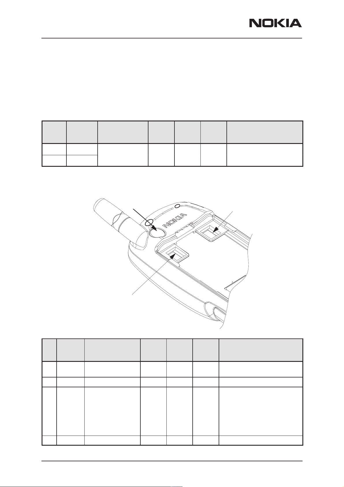
RF Connector
The RF-connector is needed to utilize the external antenna with Car
Cradle. The RF-connector is located on the back side of the transceiver
on the top section. See the illustration in the next chapter.
PAMS Technical Documentation
Con-
tact
1 EXT_ANT
2 GND
Line
Symbol
Battery Contacts
Parameter Mini-
mum
p
Typical
/ Nomi-
nal
Maxi-
mum
Unit / Notes
External antenna connec-
,
0 V DC
Pin Line
Symbol
1 VBAT Battery voltage 3.0 3.6 5.0 V/ Maximum voltage in idle
2 BSI Input voltage Battery size indication
3 BTEMP Input voltage
4 GND 0 0 V
Page 8
Parameter Mini-
Input voltage
Output voltage
PWM output signal
frequency
Nokia Mobile Phones Ltd.
Typical
mum
0
2.1
1.9
20 22
/ Nomi-
nal
Maxi-
mum
1.4
3
2.8
25
Unit / Notes
mode with charger connected
V/ Battery temperature indication
V/ Phone power up (pulse)
V/ Battery power up (pulse)
kHz/ PWM to VIBRA BA T-
TERY
Issue 1 10/00
Page 15

PAMS Technical Documentation
NSW-5 Series Transceivers
System Module UT5U
Issue 1 10/00 Nokia Mobile Phones Ltd.
Page 16
NSW-5
System Module UT5U
AMENDMENT RECORD SHEET
PAMS Technical Documentation
Amendment
Number
Date Inserted By Comments
Issue1 10/00 OJuntune
Page 2
Nokia Mobile Phones Ltd.
Issue 1 10/00
Page 17

PAMS Technical Documentation
CONTENTS
Schematic Diagrams: 5. . . . . . . . . . . . . . . . . . . . . . . . . . . . . . .
Vocabulary 6. . . . . . . . . . . . . . . . . . . . . . . . . . . . . . . . . . . . . . . . . . . . .
Transceiver NSW–5 7. . . . . . . . . . . . . . . . . . . . . . . . . . . . . . . . . . . . .
Introduction 7. . . . . . . . . . . . . . . . . . . . . . . . . . . . . . . . . . . . . . . . . .
Interconnection Diagram 7. . . . . . . . . . . . . . . . . . . . . . . . . . . . . .
System Connector 8. . . . . . . . . . . . . . . . . . . . . . . . . . . . . . . . .
User Interface (UI) 10. . . . . . . . . . . . . . . . . . . . . . . . . . . . . . . . . . . .
Display 10. . . . . . . . . . . . . . . . . . . . . . . . . . . . . . . . . . . . . . . . . . .
Roller key 10. . . . . . . . . . . . . . . . . . . . . . . . . . . . . . . . . . . . . . . . .
Slide sensor switch 11. . . . . . . . . . . . . . . . . . . . . . . . . . . . . . . . .
UI contacts on the Engine module 12. . . . . . . . . . . . . . . . . . . .
Submodules 12. . . . . . . . . . . . . . . . . . . . . . . . . . . . . . . . . . . . . . . . .
List of Submodules 12. . . . . . . . . . . . . . . . . . . . . . . . . . . . . . . . .
Operation Modes 13. . . . . . . . . . . . . . . . . . . . . . . . . . . . . . . . . . . . .
Active Operation 13. . . . . . . . . . . . . . . . . . . . . . . . . . . . . . . . . . . . .
Analog Control Channel mode (ACCH) 13. . . . . . . . . . . . . . . .
Analog Voice Channel Mode (AVCH) 14. . . . . . . . . . . . . . . . .
Digital Control Channel Mode (DCCH) 14. . . . . . . . . . . . . . . .
Digital Traffic Channel Mode (DTCH) 14. . . . . . . . . . . . . . . . .
Out of Range Mode (OOR) 15. . . . . . . . . . . . . . . . . . . . . . . . . .
Power Distribution 16. . . . . . . . . . . . . . . . . . . . . . . . . . . . . . . . . . . .
Block Diagram of power distribution 16. . . . . . . . . . . . . . . . . .
Technical Summary of power distribution 16. . . . . . . . . . . . . .
Charging Control 17. . . . . . . . . . . . . . . . . . . . . . . . . . . . . . . . . . . . .
Two–wire charging 17. . . . . . . . . . . . . . . . . . . . . . . . . . . . . . . . .
Three–wire charging 18. . . . . . . . . . . . . . . . . . . . . . . . . . . . . . . .
Watchdog 18. . . . . . . . . . . . . . . . . . . . . . . . . . . . . . . . . . . . . . . . . . .
Power up 19. . . . . . . . . . . . . . . . . . . . . . . . . . . . . . . . . . . . . . . . . . . .
Power up when power–button is pushed 19. . . . . . . . . . . . . .
Power up when charger connected 20. . . . . . . . . . . . . . . . . . .
Normal battery voltage 20. . . . . . . . . . . . . . . . . . . . . . . . . . .
Empty battery 21. . . . . . . . . . . . . . . . . . . . . . . . . . . . . . . . . . .
IBI (Intelligent Battery Interface) 22. . . . . . . . . . . . . . . . . . .
Mixed trigger to power up 22. . . . . . . . . . . . . . . . . . . . . . . . .
Power Down 22. . . . . . . . . . . . . . . . . . . . . . . . . . . . . . . . . . . . . . . . .
Controlled Power Down 22. . . . . . . . . . . . . . . . . . . . . . . . . . . . .
Power down pushing PWR–key 22. . . . . . . . . . . . . . . . . . . .
Power down when battery voltage is discharged too low 22
Power down with fault in the transmitter 22. . . . . . . . . . . . .
Uncontrolled Power Down 23. . . . . . . . . . . . . . . . . . . . . . . . . . .
Power down when watchdog expires 23. . . . . . . . . . . . . . .
Power down with Battery disconnected 23. . . . . . . . . . . . .
Battery disconnected when charger is connected 23. . . .
NSW-5
System Module UT5U
Issue 1 10/00
Nokia Mobile Phones Ltd.
Page 3
Page 18

NSW-5
System Module UT5U
Circuit Description of Submodules 24. . . . . . . . . . . . . . . . . . . . . .
CTRLU 24. . . . . . . . . . . . . . . . . . . . . . . . . . . . . . . . . . . . . . . . . . .
MCU main features 24. . . . . . . . . . . . . . . . . . . . . . . . . . . . . . . . .
DSP main features 25. . . . . . . . . . . . . . . . . . . . . . . . . . . . . . . . .
System Logic main features 26. . . . . . . . . . . . . . . . . . . . . . . . .
Memories 26. . . . . . . . . . . . . . . . . . . . . . . . . . . . . . . . . . . . . . . . .
AUDIO–RF 27. . . . . . . . . . . . . . . . . . . . . . . . . . . . . . . . . . . . . . . .
COBBA main features 27. . . . . . . . . . . . . . . . . . . . . . . . . . . . . .
PWRU 27. . . . . . . . . . . . . . . . . . . . . . . . . . . . . . . . . . . . . . . . .
CCONT Main Features 27. . . . . . . . . . . . . . . . . . . . . . . . . . . . .
CHAPS Main Features 28. . . . . . . . . . . . . . . . . . . . . . . . . . . . . .
INF 28. . . . . . . . . . . . . . . . . . . . . . . . . . . . . . . . . . . . . . . . . . . . . . . . .
User Interface 29. . . . . . . . . . . . . . . . . . . . . . . . . . . . . . . . . . . . . . . .
UISWITCH main features 30. . . . . . . . . . . . . . . . . . . . . . . . . . .
RF Module 31. . . . . . . . . . . . . . . . . . . . . . . . . . . . . . . . . . . . . . . . . . . . .
Technical Summary 31. . . . . . . . . . . . . . . . . . . . . . . . . . . . . . . . . . .
RF Frequency Plan 31. . . . . . . . . . . . . . . . . . . . . . . . . . . . . . . . . . .
DC Characteristics 32. . . . . . . . . . . . . . . . . . . . . . . . . . . . . . . . . . . .
Power Distribution Diagram 32. . . . . . . . . . . . . . . . . . . . . . . . . .
Regulators 34. . . . . . . . . . . . . . . . . . . . . . . . . . . . . . . . . . . . . . . .
Receiver 34. . . . . . . . . . . . . . . . . . . . . . . . . . . . . . . . . . . . . . . . . . . .
DAMPS800 RX 34. . . . . . . . . . . . . . . . . . . . . . . . . . . . . . . . . . . .
TDMA 1900 RX 35. . . . . . . . . . . . . . . . . . . . . . . . . . . . . . . . . . . .
Frequency Synthesizers 35. . . . . . . . . . . . . . . . . . . . . . . . . . . . . . .
DAMPS 800 operation 36. . . . . . . . . . . . . . . . . . . . . . . . . . . . . .
TDMA 1900 operation 36. . . . . . . . . . . . . . . . . . . . . . . . . . . . . .
Transmitter 36. . . . . . . . . . . . . . . . . . . . . . . . . . . . . . . . . . . . . . . . . .
DAMPS800 TX 36. . . . . . . . . . . . . . . . . . . . . . . . . . . . . . . . . . . .
TDMA1900 TX 37. . . . . . . . . . . . . . . . . . . . . . . . . . . . . . . . . . . . .
DAMPS800/TDMA1900 operation 37. . . . . . . . . . . . . . . . . . . . . .
Supply voltages in different modes of operation 37. . . . . . . .
Software Compensations 37. . . . . . . . . . . . . . . . . . . . . . . . . . . . . .
Power Levels (TXC) vs. Temperature 37. . . . . . . . . . . . . . . . .
Power Levels (TXC) vs. Channel 38. . . . . . . . . . . . . . . . . . . . .
Power levels vs. Battery Voltage 38. . . . . . . . . . . . . . . . . . . . .
TX Power Up/Down Ramps 38. . . . . . . . . . . . . . . . . . . . . . . . .
Modulator Output Level 38. . . . . . . . . . . . . . . . . . . . . . . . . . . . .
Digital Mode RSSI 38. . . . . . . . . . . . . . . . . . . . . . . . . . . . . . . . . .
PAMS Technical Documentation
RF Block Specifications 38. . . . . . . . . . . . . . . . . . . . . . . . . . . . . . . . . .
Receiver 38. . . . . . . . . . . . . . . . . . . . . . . . . . . . . . . . . . . . . . . . . . . .
DAMPS 800MHz RX Front End 38. . . . . . . . . . . . . . . . . . . . . .
TDMA 1900MHz RX Front End 39. . . . . . . . . . . . . . . . . . . . . .
1st IF Amplifier 39. . . . . . . . . . . . . . . . . . . . . . . . . . . . . . . . . . . . .
Analog IF parts 39. . . . . . . . . . . . . . . . . . . . . . . . . . . . . . . . . . . .
Digital IF parts 40. . . . . . . . . . . . . . . . . . . . . . . . . . . . . . . . . . . . .
Page 4
Nokia Mobile Phones Ltd.
Issue 1 10/00
Page 19

PAMS Technical Documentation
Transmitter 41. . . . . . . . . . . . . . . . . . . . . . . . . . . . . . . . . . . . . . . . . .
Synthesizers 41. . . . . . . . . . . . . . . . . . . . . . . . . . . . . . . . . . . . . .
Output levels 41. . . . . . . . . . . . . . . . . . . . . . . . . . . . . . . . . . . .
Parts Lists
Engine Module UT5U (0201142) 49. . . . . . . . . . . . . . . . . . . . . . . .
Schematic Diagrams:
Block Diagram of UT5 (Version 17.4 Edit 40) A–1. . . . . . . . . . . . . . .
Circuit Diagram of CTRLU Block (Version 17.4 Edit 441) A–2. . . . .
Circuit Diagram of PWRU (Version 17.4 Edit 474 ) A–3. . . . . . . . .
NSW-5
System Module UT5U
Page No
Circuit Diagram of Audio (Version 17.4 Edit 391) A–4. . . . . . . . . . .
Circuit Diagram of Receiver (Version 17.4 Edit 39) A–5. . . . . . . . . .
Circuit Diagram of Synthesiser Block (Version 17.4 Edit 17) A–6.
Circuit Diagram of Transmitter (Version 17.4 Edit 51) A–7. . . . . . . .
Circuit Diagram of UI (Version 17.4 Edit 179) A–8. . . . . . . . . . . . . . .
Circuit Diagram of IR (Version 17.4 Edit 99)
and BB_RF interface (Version 17.4 Edit 96) A–9. . . . . . . . . . . . . . . .
Diagram of Dualband RF (Version 17.4 Edit 10) A–10. . . . . . . . . . . .
Layout Diagram of UT5U v.17_4 side 1/2 A–11. . . . . . . . . . . . . . . . .
Layout Diagram of UT5U v.17_4 2/2 A–12. . . . . . . . . . . . . . . . . . . . . .
Issue 1 10/00
Nokia Mobile Phones Ltd.
Page 5
Page 20

NSW-5
System Module UT5U
Vocabulary
CS = Cellular System
DCT = Digital Core Technology
HW = Hardware (drivers)
PC = Personal Computer
RAM = Random Access Memory
ROM = Read Only Memory
SPEC = Specification
SW = Software
TDMA = Time Division Multiple Access
LCD = Liquid Crystal Display
FSTN = Film Compensated Super Twist Nematic
COG = Chip On Glass
ASIC = Application Specific Integrated Circuit
DSP = Digital Signal Processor
DTMF = Dual Tone Multi–Frequency
DTX = Discontinuous Transmission
EEPROM = Electrically Erasable Programmable Read–Only Memory
EFR = Enhanced Full Rate codec
EM = Energy Management
IF = Interface, Intermediate Frequency
IR = Infrared
IrDa = Infrared Data
RISC = Reduced Instruction Set Controller
SCM = Short Code Memory
SMS = Short Message Services
MO = Mobile Originated
MT = Mobile Terminated
SW = Software
UI = User Interface
PWB = Printed Wiring Board
Engine = Radio Module
PAMS Technical Documentation
Page 6
Nokia Mobile Phones Ltd.
Issue 1 10/00
Page 21
PAMS Technical Documentation
Transceiver NSW–5
Introduction
The NSW–5 is a dualband/dualmode radio transceiver unit fror the US
TDMA 800/1900MHz networks. The transceiver is fully based on 3V
technology.
The transceiver consists System/RF/keypad module (UT5), sub as-
sembled LCD module and assembly parts.
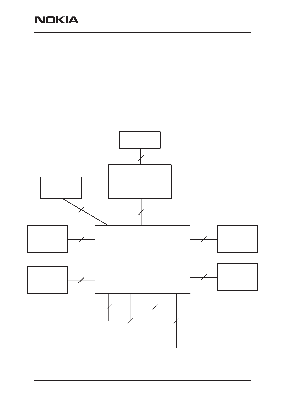
Interconnection Diagram
NSW-5
System Module UT5U
Earpiece
2
Buzzer
Antenna
Slide
Sensor
Display
Module
2
14
1
4
Battery
System/RF
Module
2
UT5
3 + 36
2
MIC
Issue 1 10/00
2
System
Connector
RF
Connector
Nokia Mobile Phones Ltd.
Charger
5
IR
Page 7
Page 22
NSW-5
System Module UT5U
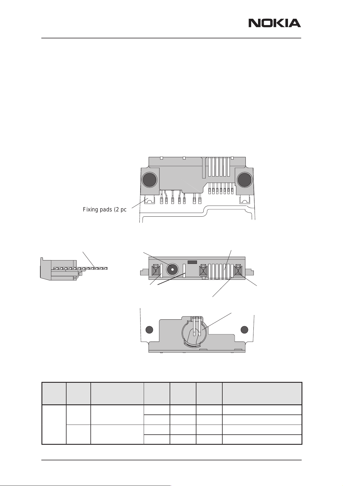
System Connector
The System connector provides
– 9 contact pads
– 3–pole round DC–jack for charging
– Cavity and 2 contact springs for Slide Sensor Switch
The System Connector diagrams are below:
B side view
PAMS Technical Documentation
2 for charging (Charge Voltage and Charging Control (PWM) )
6 for accessory interface
common GND
Engine PWB
A side view
Fixing pads (2 pcs)
DC Jack
Charger pads (2 pcs)
1
Common GND pad
8
7
14
Accessory
connector (6 pads)
Cable locking holes (3 pcs)
Cavity and contact springs for
Slide Sensor Switch
The System connector pin and signal listing is in the next table:
Con-
tact
pin
1 VIN Charger input
Page 8
Line
Sym-
bol
VIN Charger input
Parameter Mini-
voltage
current
Nokia Mobile Phones Ltd.
Typical
mum
6.0 V/ Unloaded ACP-8 Charger
7.24 7.6 7.95 V/ Unloaded ACP–7 Charger
320 370 420 mA/ Supply current
/ Nomi-
nal
650 mA/ Supply current
Maxi-
mum
Unit / Notes
Issue 1 10/00
Page 23
PAMS Technical Documentation
G
JACK
JACK
NSW-5
System Module UT5U
Con-
tact
pin
CHARGER
JACK
(2)
CHAR-
ER
A
(3)
CHARGER
(4)
5 CHRG
Slide
switch
(6)
Slide
switch
(7)
8 XMIC Input
9 SGND Signal ground 0 0 mVrms
Sym-
bol
L_GND Charger ground
VIN Charger input
K
CHRG
CTRL
CTRL
SLIDE SLIDE OPEN/
L_GND SLIDE SWITCH
ParameterLine
input
voltage
Charger input
current
Output
high voltage
PWM frequency 32 Hz /PWM frequency for
Output
high voltage
PWM frequency 32 Hz /PWM frequency for
CLOSE
GND
signal voltage
Minimum
0 0 0 V/ Supply ground
7.1 8.4 9.3 V/ Unloaded ACP-8 Charger
720 800 850 mA/ Supply current
7.24 7.6 7.95 V/ Unloaded ACP–7 Charger
320 370 420 mA/ Supply current
2.0 2.8 V/ Charger control (PWM)
2.0 2.8 V/ Charger control (PWM)
2.7 2.8 2.85 V/ Contact in microphone
0 0 0 V/ Contact in microphone
Typical
/ Nomi-
nal
60 1 Vpp mVrms
mum
high
charger
high
charger
cavity.
cavity.
Unit / NotesMaxi-
10 XEAR Output
signal voltage
11 MBUS
12 FBUS_
RX
13 FBUS_
TX
14 L_GND Common ground
I/O low voltage 0 0.8
I/O high voltage 2.0 2.8
Input low voltage 0 0.8 V/ Fbus receive.
Input high voltage 2.0 2.8 V/ Serial Data, Baud rate
Output low voltage 0 0.8 V/ Fbus transmit.
Output
high voltage
input
80 1 Vpp mVrms
V/Serial bidirectional control
bus. Baud rate 9600 Bit/s
9.6k–230.4kBit/s
2.0 2.8 V/ Serial Data, Baud rate
9.6k–230.4kBit/s
0 0 0 V/ Supply ground
Issue 1 10/00
Nokia Mobile Phones Ltd.
Page 9
Page 24
NSW-5
System Module UT5U
User Interface (UI)
Radio module provides the connections for keymat, roller key, mic, buzzer
and display module. Slide sensor switch is placed in bottom connector.
Microphone lines in slide are connected to the PWB via contacts on
A–cover. Speaker is connected to display module.
Display
Display assembly (figure below) consists of LCD, flexfoil with power key
and pads for speaker and LEDs for back light, PWB connector, Plastic
lens with ESD shield and light guide parts which also hold the assembly
parts together.
PAMS Technical Documentation
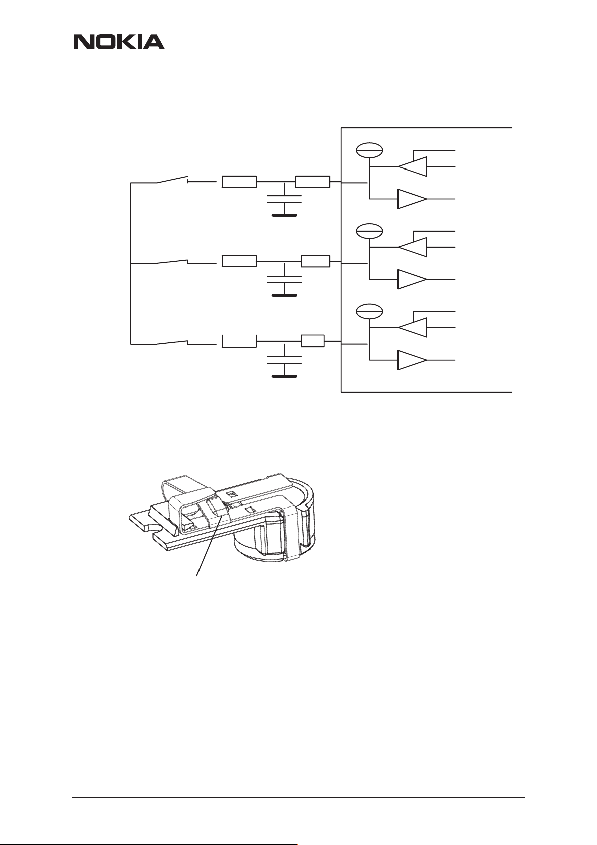
Roller key
The roller is a state type encoder. It has 3 states, the contact arrange-
ment is shown in the following table, ”x” marks a closed contact.
Page 10
Position Contact A Contact B Contact C
1 x x
2 x x
3 x x
Nokia Mobile Phones Ltd.
Issue 1 10/00
Page 25
PAMS Technical Documentation
The roller key schematic diagram is below.
NSW-5
System Module UT5U
MAD
Switches shown in pos 1.
A
B
C
Slide sensor switch
Pullup
Pullup
Pullup
Drive
0
A
Drive
0
B
Drive
0
C
A custom connector for sensing if the Slide is open or closed. Connector
guides in to the Microphone Cavity in the System Connector.
The hook in slide cover will hit here.
When the slide is closed, there is no
electrical contact between the springs.
Issue 1 10/00
Nokia Mobile Phones Ltd.
Page 11
Page 26
NSW-5
System Module UT5U
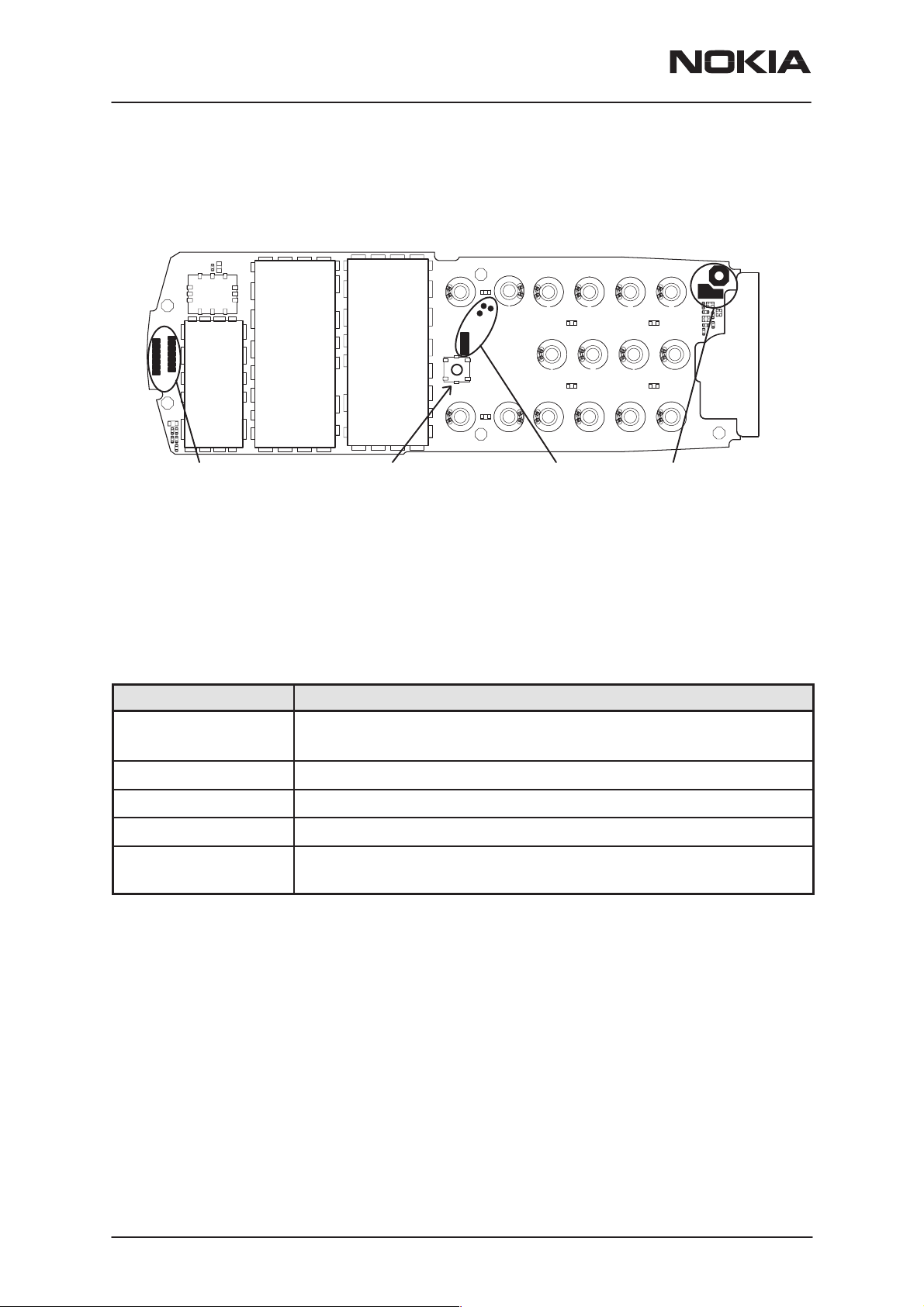
UI contacts on the Engine module
PAMS Technical Documentation
PADs for Display
Assembly connector
Roller key
switch
PADs for
roller key
Microphone contacts
through A cover to Slide
Submodules
List of Submodules
Name of submodule Function
CTRLU Control Unit for the phone, comprising MAD ASIC (MCU,
DSP, System Logic) and Memories
PWRU Power supply, comprising CCONT and CHAPS
AUDIO–RF_IF Audio coding and RF–BB interface, COBBA
INF Infrared transceiver
UI User interface; UISWITCH, keyboard LEDs, and UI pad
areas
Page 12
These blocks are only functional blocks and therefore have no type nor
material codes. For block diagram, see the baseband schematics on the
syst–level.
Nokia Mobile Phones Ltd.
Issue 1 10/00
Page 27

PAMS Technical Documentation
Operation Modes
The transceiver has five different operation modes:
– Power off
– Idle
– Active
– Charge
– Local
In the Power off mode only the circuits needed for power up are supplied.
In the Idle mode circuits are powered down and only sleep clock is run-
ning.
In the Active mode all the circuits are supplied with power altough some
parts might be in the idle state part of the time.
NSW-5
System Module UT5U
The Charge mode is effective in parallel with previous modes. The charge
mode itself consists of two different states, i.e. the charge and the maintenance charge mode.
The Local mode is used for testing and alignment.
Active Operation
The phone has the following Active Operation modes:
– Analog mode, on 800 MHz band
– Analog Control Channel ACCH
– Analog Voice Channel AVCH
– Digital mode, on 800 MHz band
– Digital Control Channel DCCH
– Digital Traffic Channel DTCH
– Digital mode, on 1900 MHz band
– Digital Control Channel DCCH
– Digital Traffic Channel DTCH
– Out Of Range –mode OOR
If the phone cannot find signal from the base station on any control chan-
nel (analog or digital) it goes into OOR mode for power saving.
Analog Control Channel mode (ACCH)
On analog control channel the phone receives continuous signalling messages on Forward Control Channel (FOCC) from base station, being
most of the time in IDLE mode. Only the receiver part is on. Occasionally
phone re–scans control channels in order to find the stronger or other-
Issue 1 10/00
Nokia Mobile Phones Ltd.
Page 13
Page 28

NSW-5
System Module UT5U
wise preferred control channel. Also registration (TX on) happens occasionally, where phone sends its information on Reverse Control Channel
(RECC) to base station and the phone’s location is updated in the switching office.
If a call is initiated, either by the user or base station, the phone moves to
analog voice channel or digital traffic channel mode depending on the orders by the base station.
Analog Voice Channel Mode (AVCH)
The phone receives and transmits analog audio signal. All circuitry is
powered up except digital rx–parts. In this mode DSP does all the audio
processing, and in the Hands Free (HF) mode it also performs echo–cancellation and the HF algorithm. COBBA makes AD–conversion for MIC
signal, and DA–conversion for EAR signal.
With audio signal also SAT (Supervisory Audio Tone) is being received
from the base station. The SAT signal can be 5970 Hz, 6000Hz or 6030
Hz, the frequency being defined by the base station. DSP’s DPLL phase
lock loops to SAT, detects if the SAT frequency is the expected one and
examines the signal quality. DSP reports SAT quality figures to MCU regularly. The received SAT signal is transponded (transmitted back) to base
station.
PAMS Technical Documentation
Base station can send signalling messages on Forward Voice Channel
(FVC) to the phone, by replacing the audio with a burst of Wide Band
Data (WBD). Typically these are handoff or power level messages. System Logic RX–modem is used for receiving the signalling message burst,
after which it gives interrupt to MCU for reading the data. During the burst
audio path must be muted; MCU gives message to DSP about this. MCU
can acknowledge the messages on Reverse Voice Channel (RVC), where
DSP sends the WBD to transmitter RF.
Digital Control Channel Mode (DCCH)
On digital control channel (DCCH) the DSP receives the paging information from the Paging channels. DSP sends messages to MCU for processing them.
Phone uses sleep mode between received time slots. Then DSP sets the
sleep clock timer and MCU, DSP and RF including VCXO are powered
down. Only sleep clock and necessary timers are running.
From DCCH phone may be ordered to analog control channel or to analog or digital traffic channel.
Digital Traffic Channel Mode (DTCH)
Page 14
On digital voice channel the DSP processes speech signal in 20 ms time
slots. DSP performs the speech and channel functions in time shared
fashion and sleeps whenever possible. Rx and tx are powered on and off
Nokia Mobile Phones Ltd.
Issue 1 10/00
Page 29

PAMS Technical Documentation
according to the slot timing. MCU is waken up mainly by DSP, when
there is signalling information for the Cellular Software.
In Digital Data Channel Mode audio processing is not needed and the audio circuitry can be shut down. Otherwise the mode is similar to Digital
Voice Channel Mode.
Out of Range Mode (OOR)
If the phone cannot find signal from the base station on any control channel (analog or digital) it can go into OOR mode for power saving.
All RF circuits are powered off and baseband circuits are put into low
power mode, VCXO is stopped and only sleep clock is running in MAD
and CCONT. After the programmable timer in MAD has elapsed the
phone turns receiver on and tries to receive signalling data from base station. If it succeeds, the phone goes to standby mode on analog or digital
control channel. If the connection can not be established the phone will
return to out of range mode, until the timer elapses again.
NSW-5
System Module UT5U
Issue 1 10/00
Nokia Mobile Phones Ltd.
Page 15
Page 30
NSW-5
System Module UT5U
Power Distribution
In normal operation the baseband is powered from the phone‘s battery.
An external charger recharges the battery. The charger can be either a
standard charger that can deliver around 350 mA or so called performance charger, which can deliver supply current up to 850 mA.
The baseband contains components that control power distribution to
whole phone excluding those parts that use continuous battery supply.
The battery feeds power directly to following parts of the system: CCONT,
power amplifier, and UI (buzzer, display, keyboard lights, IR and vibra).
Figure below shows a block diagram of the power distribution.
The power management circuit CHAPS provides protection agains overvoltages, charger failures and pirate chargers etc. that would otherwise
cause damage to the phone.
Block Diagram of power distribution
PAMS Technical Documentation
VCXO
CHAPS
VCHAR
BATTERY
MAD
VBAT
CCONT
VR1
PWM
VR6
VBB
V2V
VBB
V5V
Vref
Technical Summary of power distribution
SIO
COBBA LCD–DRVR
FLASH
RF
VR1–VR5,
VR7
Page 16
Battery voltage VBAT is connected to CCONT which regulates the supply
voltages VBB, VR1–VR7, VSIM and V5V. CCONT enables automatically
VR1, VBB, V2V, VR6 and Vref in power–up.
VBB is used as baseband power supply for all digital parts. It is constantly
on when the phone is powered up. VSIM is used as programming voltage for the Flash memory when SW is writing a backup of EEPROM data
during power–down with the power key.
Nokia Mobile Phones Ltd.
Issue 1 10/00
Page 31

PAMS Technical Documentation
V5V is used for RF parts only. It can be switched off by the RFCEN signal.
VR1 is used for the VCXO supply, and VR6 is used in COBBA for analog
parts. RFCEN signal to CCONT controls both VR1 and VR6 regulators;
they can be switched off in sleep modes, and during standby. During
sleep VR6 output pin is connected to VBB regulator inside CCONT.
CCONT regulators are controlled either through SIO from MAD or timing
sensitive regulators are controlled directly to their control pins. These two
control methods form a logical OR–function, i.e. the regulator is enabled
when either of the controls is active. Most of the regulators can be controlled individually.
CHAPS connects the charger voltage (VCHAR) to battery. MCU of MAD
controls the charging through CCONT. MAD sets the parameters to
PWM–generator in CCONT and PWM–output controls the charging voltage in charger.
When the battery voltage is below 3.0V, CHAPS controls independently
the charging current.
NSW-5
System Module UT5U
Charging Control
Charging is controlled by MCU SW, which writes control data to CCONT
via serial bus. CCONT output pin PWMOUT (Pulse Width Modulation)
can be used to control both the charger and the CHAPS circuit inside
phone. Charging control diagram below.
Vin
System
Connector
PWMOUT
To
charger
Charging Control
CHAPS
BATTERY
MAD
CCONT
serial control
Two–wire charging
With 2–wire charging the charger provides constant output current, and
the charging is controlled by PWMOUT signal from CCONT to CHAPS.
The PWMOUT signal frequency set is 1 Hz, and the charging switch in
CHAPS is pulsed on and off at this frequency. The final charged energy to
battery is controlled by adjusting the PWMOUT signal pulse width.
Issue 1 10/00
Nokia Mobile Phones Ltd.
Page 17
Page 32

NSW-5
System Module UT5U
Both the PWMOUT frequency is selected and the pulse width controlled
by the MCU which writes these values to CCONT.
Three–wire charging
With 3–wire charging the charger provides adjustable output current, and
the charging is controlled by the PWMOUT signal from CCONT to charger, with the bottom connector signal. The PWMOUT signal frequency
set is 32 Hz, and the charger output voltage is controlled by adjusting the
PWMOUT signal pulse width. The charger switch in CHAPS is constantly
on in this case.
Watchdog
PAMS Technical Documentation
VCXO
LCD–DRVR
32 kHz
BATTERY
MAD COBBA
CCONT
VR1
VR6
VBB
SLCLK
MCU
LOGIC
SIO
Both MAD and CCONT include a watchdog, and both use the 32 kHz
sleep clock. The watchdog in thw MAD is the primary one, called SW–
watchdog. MCU has to update it regularly. If it is not updated, logic inside
MAD gives reset to MAD. After the reset the MCU can read an internal
status bit to see the reason for reset, whether it was from the MAD or
CCONT. The SW–watchdog delay can be set between 0 and 63 seconds
at 250 millisecond steps; and after power–up the default value is the max.
time.
Page 18
MAD must reset CCONT watchdog regularly. CCONT watchdog time can
be set through SIO between 0 and 63 seconds at 1 second steps. After
power–up the default value is 32 seconds. If watchdog elapses, CCONT
will cut off all supply voltages.
After total cut–off the phone can be re–started through any normal power–up procedure.
Nokia Mobile Phones Ltd.
Issue 1 10/00
Page 33

PAMS Technical Documentation
Power up
When the battery is connected to phone, the 32.768 kHz crystal oscillator
of the CCONT is not started until the power–button is pressed. The regulators are not started. After the crystal has started, the phone is ready to
be powered up by any of the following ways.
Power up when power–button is pushed
PWRONX
VR1, VBB, VR6,
V2V
RFCEN
RFCSETTLED
NSW-5
System Module UT5U
RFC (VCXO)
COBBACLK
PURX
SLCLK
After the PWR–key has been pushed, the CCONT gives PURX reset to
MAD and the COBBA, and turns on VR1, VBB, V2V and VR6 regulators
(if the battery voltage has exceeded 3.0 V). VR1 supplies VCXO, VBB
supplies MAD and digital parts of COBBA, and VR6 supplies analog parts
of COBBA. After the initial delay t2 the VCXO starts to give proper RFC
to COBBA that further divides it to the COBBACLK for MAD. COBBA will
output the COBBACLK only after the PURX reset has been removed. After delay t3 the CCONT releases PURX and MAD can take control of the
operation of the phone.
t1
t2
t3
t1 < 1 ms
t2 1 – 6 ms, VCXO settled
t3 62 ms, PURX delay generated by CCONT
After that MCU–SW in MAD detects that the PWR–key is still pushed and
shows the user that the phone is powering up by starting the LCD and
Issue 1 10/00
Nokia Mobile Phones Ltd.
Page 19
Page 34

NSW-5
System Module UT5U
turning on the lights. MCU–SW must start also the RF receiver parts at
this point.
V5V–regulator (for RF) default value is off in power–up, and can be controlled on via serial bus when needed.
Power up when charger connected
Normal battery voltage
VCHAR
VR1, VBB, VR6,
V2V
RFCEN
RFCSETTLED
PAMS Technical Documentation
RFC (VCXO)
COBBACLK
PURX
SLCLK
CCONTINT
The power up procedure is similar to process described in the previous
chapter with the exception that the rising edge of VCHAR triggers the
power up in CCONT.
Also CCONT sets output CCONTINT. MAD detects the interrupt, and after
that reads CCONT status register to find out the reason for the interrupt
(charger in this case). The phone will remain in the ”acting dead” state,
which means that the user interface is not activated unless the power button is pressed. Only the charging activity is indicated on the display.
t1
t2
t3
Page 20
CCONTINT is generated both in the case the charger is connected, and
in the case the charger is disconnected.
Nokia Mobile Phones Ltd.
Issue 1 10/00
Page 35

PAMS Technical Documentation
Empty battery
VBAT > 3.0 V
VCHAR
VR1, VBB, VR6,
V2V
RFCEN
RFCSETTLED
RFC (VCXO)
COBBACLK
NSW-5
System Module UT5U
PURX
SLCLK
CCONTINT
t1
t2
t3
Before battery voltage voltage rises over 3.0 V CHAPS gives an initial
charge (with limited current) to the battery. After battery voltage reaches
that voltage limit the power up procedure is as described in the previous
chapters.
Anyway, if the standard charger is connected and power–up requested
from the power button, the current consumption is kept in the minimum in
the beginning because the charger output current is rather low and the
battery voltage is on the minimum limit. Thus, the phone receiver parts
and the user interface lights are not powered up immediately, but after a
short delay.
Issue 1 10/00
Nokia Mobile Phones Ltd.
Page 21
Page 36

NSW-5
System Module UT5U
IBI (Intelligent Battery Interface)
Phone can be powered up by external device (accessory or similar) by
providing a start pulse to the battery signal BTEMP; this is detected by
CCONT. After that the power–up procedure is similar to pushing power–
button.
Mixed trigger to power up
It is possible that PWR–key is pushed during charger initiated power–up
procedure or charger is connected during PWR–key initiated power up
procedure. In this kind of circumstances the power–up procedure (from
the HW point of view) continues as nothing had happened.
When the Baseband HW is working normally and SW is running, SW detects that both conditions are fulfilled and then acts accordingly.
PAMS Technical Documentation
Power Down
Controlled Power Down
Power down pushing PWR–key
MAD (MCU SW) detects that PWR–key is pressed long enough. After that
the lights and LCD are turned off. MCU stops all the activities it was doing
(e.g. ends a call), sends power off command to CCONT (i.e. gives a short
watchdog time) and goes to idle–task. After the delay CCONT cuts all the
supply voltages from the phone.
Note that the phone does not go to power off (from HW point of view)
when the charger is connected and PWR–key is pushed. It is shown to
user that the phone is in power off, but in fact the phone is just acting being powered off (”acting dead”).
Power down when battery voltage is discharged too low
During normal discharge the phone indicates the user that the battery will
drain after some time. If not recharged, SW detects that battery voltage is
too low and shuts the phone off through a normal power down procedure.
Anyway, if the SW fails to power down the phone, the CCONT will make a
reset and power down the phone if the battery voltage drops below 2.6 –
2.9 V.
Power down with fault in the transmitter
If MAD receives fault indication, from the line TXF, that the transmitter is
on although it should not be, the control SW will power down the phone.
Page 22
Nokia Mobile Phones Ltd.
Issue 1 10/00
Page 37

PAMS Technical Documentation
Uncontrolled Power Down
NSW-5
System Module UT5U
Power down
when watchdog expires
If the SW fails to update the watchdog, the watchdog will eventually expire and CCONT cuts all the supply voltages from the phone.
Power down with Battery disconnected
When battery is disconnected, immediate and totally uncontrolled power–
down happens. Therefore a power off procedure in this case can not be
described. One possible risk is that if the MCU is writing something to
Flash exactly at the same moment, the memory contents may be corrupted.
Battery disconnected when charger is connected
From hardware point of view the phone could otherwise continue functioning normally, but if the charger voltage is higher than the maximum
allowed battery voltage, this can damage the RF parts. Therefore, there
must be hardware protection against this in CHAPS.
If the user presses the PWR–key, the phone can wake up to detect that
the battery is not present (no BTYPE and /or BTEMP). After that the
phone either turns itself off or goes to low current mode (can be decided
by MCU SW).
This state does not harm the phone. The phone can not be used only
from the charger without the battery.
Issue 1 10/00
Nokia Mobile Phones Ltd.
Page 23
Page 38

NSW-5
System Module UT5U
Circuit Description of Submodules
CTRLU
CTRLU comprises MAD ASIC (MCU, DSP, System Logic) and Memories.
The soldering connections of the IC are unaccessible for probing, only
test points can be used. Therefore no pin list is published.
The environment consists of two memory circuits (FLASH,SRAM), a
22–bit address bus and a 16–bit data bus. Besides there are
ROM1SELX, ROM2SELX and RAMSELX signals for chip selection.
MCU main features
– System control
PAMS Technical Documentation
– Cellular Software (CS)
Cellular Software takes care of communication with switching office,
as well call build–up, maintenance and termination.
– Communication control
M2BUS is used to communicate to external devices. This interface is
also used for service and maintenance purposes.
– User Interface (UI)
PWR–key, keyboard, LCD, backlight, mic, ear and alert (buzzer, vibra,
led) control.
Serial interface from MAD to LCD (common for CCONT).
– Authentication
Authentication is used to prevent fraud usage of cellular phones.
– RF monitoring
RF temperature monitoring by VCXOTEMP, ADC in CCONT.
Received signal strength monitoring by RSSI, ADC in CCONT.
False transmission detection by TXF signal, digital IO–pin.
– Power up/down and Watchdog control
When power key is pressed, initial reset (PURX) has happened and default regulators have powered up in CCONT, MCU and DSP take care of
the rest of power up procedures (LCD, COBBA, RF).
MCU must regularly reset Watchdog counter in CCONT, otherwise
the power will be switched off.
– accessory monitoring
Accessory detection by EAD (XMIC/HEADSETINT), AD–converter in
CCONT.
Connection (FBUS) for data transfer.
Page 24
Nokia Mobile Phones Ltd.
Issue 1 10/00
Page 39

PAMS Technical Documentation
– battery and charging monitoring
MCU reads the battery type (BTYPE), temperature (BTEMP) and voltage
(VBAT) values by AD–converter in CCONT, and phone’s operation is allowed only if the values are reasonable. Charging current is controlled by
writing suitable values to PWM control in CCONT.
MCU reads also charger voltage (VCHAR) and charging current values
(IBAT).
– production/after sales tests and tuning
Flash and EEPROM loading, baseband tests, RF tuning
– Control of CCONT via serial bus
MCU writes controls (regulators on/off, Watchdog reset, charge
PWM control) and reads AD–conversion values.
For AD–conversions MCU gives the clock for CCONT (bus clock),
because the only clock in CCONT is sleep clock, which has too low frequency.
NSW-5
System Module UT5U
DSP main features
The DSP (Digital Signal Processor) is in charge of the channel and
speech coding according to the IS–136 specification. The block consists
of a DSP and internal ROM and RAM memory. The input clock is 9.72
MHz, and DSP has an own internal PLL–multiplier. Main interfaces are to
MCU, and via System Logic to COBBA and RF.
– Analog transmit
Audio signal in analog mode is fed to the COBBA codec, where it is
routed, amplified and converted by internal A/D converter into bitstream
(the sample rate is in digital mode 8.0 kHz and in analog mode 8.1 kHz).
The digitized speech is processed by the DSP audio modules into 48.6
kHz audio. This audio is FM modulated into I/Q samples at 97.2 kHz. The
samples are sent via System Logic transmit buffer to the COBBA TXI/Q
D/A converters. This I/Q modulated analog signal goes then to RF unit
I/Q inputs. DSP must also perform echo cancelling in HF mode.
– Analog receive
In analog receive the signal is demodulated by DEMO (block in COBBA)
and the sample rate is 48.6 kHz. The samples are directed trough System Logic to DSP. DSP performs audio processing and finally transfers
the digital audio (8.1 kHz sample rate) back to COBBA, where they are
D/A converted. Resulting audio signal is routed and amplified to the earpiece or external loudspeaker.
– Digital transmit
In digital transmit mode DSP processes speech data in 20 ms slots. It
performs speech encoding (EFR), CRC generation, convolutional coding
and interleaving. Finally it sends the symbols to the System Logic modulator. The modulator performs the π/4 DQPSK modulation. System Logic
Issue 1 10/00
Nokia Mobile Phones Ltd.
Page 25
Page 40

NSW-5
System Module UT5U
controls the transmit timing and at specified intervals sends the I/Q samples at 97.2 kHz to COBBA for TXI/Q D/A converters.
– Digital receive
In digital receive mode the second IF is 450 kHz, which is sampled at
194,4 kHz in COBBA, aliased to 61,2 kHz and then downconverted and
demodulated in DSP. The timing is controlled by System Logic. DSP performs bit detection with equalizer and then convolutional decoding and
CRC checking. After this the (speech) bits are passed for speech decoding (EFR). The decoded bits are converted to analog signal in COBBA,
then routed and fed to the earpiece.
– Analog modem functions
On the analog voice channel, DSP performs the signalling functions: SAT
receiving and transponding. Transmit function: ST and wide band data.
– Control and general functions
In all modes DSP controls the RF. Controlling is done physically through
System Logic, where all necessary timing functions are implemented, and
control I/O lines are provided for e.g. synthesizer loading, power control
etc.
PAMS Technical Documentation
In all transmit modes DSP takes care of the transmitted power control
(TXC) and frequency control (AFC). Also DTMF tone generation is made
in DSP.
All clocks and timing are generated from the RFC clock. In sleep mode
only the 32 kHz clock is used.
System Logic main features
– MCU related clocking, timing and interrupts (CTIM)
– DSP related clocking, timing and interrupts (CTID)
– DSP general IO–port
–reset and interrupts to MCU and DSP
– interface between MCU and DSP (API)
– MCU interface to System Logic (MCUif)
– MCU controlled PWMs, general IO–port and USART for MBUS (PUP)
– Receive Modem (Rxmodem)
– Interface to Keyboard, CCONT and LCD Drivers (UIF)
– Interface to MCU memories, address lines and chip select decoding
(BUSC)
– DSP interface to System Logic (DSPif)
– serial accessory interface (AccIf, DSP–UART)
– Modulation, transmit filter and serial interface to COBBA (MFI)
– Serial interface for RF synthesizer control (SCU)
Memories
Page 26
FLASH
– size 2048k * 16 bit
Nokia Mobile Phones Ltd.
Issue 1 10/00
Page 41

PAMS Technical Documentation
contains the main program code for the MCU, and is able to emulate
EEPROM.
SRAM
– size 256k * 16 bit
AUDIO–RF
Audio interface and baseband–RF interface converters are integrated into
the COBBA circuit.
COBBA main features
The codec includes microphone and earpiece amplifier and all the necessary switches for routing. There are two different possibilities for routing;
internal and external devices. There are also all the AD– and DA– converters for the RF interface.
NSW-5
System Module UT5U
PWRU
A slow speed DA–converter provides automatic frequency control (AFC).
In addition, there is a DA–converters for transmitter power control (TXC).
COBBA also passes the RFC (19.44 MHz) to MAD as COBBACLK (9.72
MHz).
COBBA is connected to MAD via two serial busses:
– RXTXSIO, for interfacing the RF–DACs and DEMO; and also for audio
codec and general control. Signals used: COBBACLK (9.72 MHz, from
COBBA), COBBACSX, COBBASD (bi–directional data) and COBBADAX (data ready flag for rx–samples).
– Codec SIO, for interfacing the audio ADCs / DACs (PCM–samples).
Signals: PCMDCLK (data clock 1.08 MHz / 1.215 MHz), PCMSCLK
(frame sync 8.0 kHz / 8.1 kHz), PCMTxdata and PCMRxdata.
A vibra alerting device is used for giving silent signal to the user of an incoming call. The device is controlled with a VibraPWM output signal from
MAD. The vibra alert can be adjusted either by changing the pulse width
or by changing the pulse frequency.
CCONT Main Features
CCONT generates regulated supply voltages for baseband and RF.
There are seven 2.8 V linear regulators for RF, one 2.8 V regulator for
baseband, one special switched output (VR1_SW), one programmable 2
V output (V2V), one 3/5 V output, one 5 V output, and one 1.5 V +/– 1.5
% reference voltage for RF and COBBA.
Other functions include:
– power up/down procedures and reset logic
Issue 1 10/00
Nokia Mobile Phones Ltd.
Page 27
Page 42

NSW-5
System Module UT5U
– charging control (PWM), charger detection
– watchdog
– sleep clock (32 kHz) and control
– 8–channel AD–converter.
CHAPS Main Features
CHAPS comprises the hardware for charging the battery and protecting
the phone from over–voltage in charger connector.
The main function are
– transient, over–voltage and reverse charger voltage protection
– limited start–up charge current for a totally empty battery
– voltage limit when battery removed
– with SW protection against too high charging current
PAMS Technical Documentation
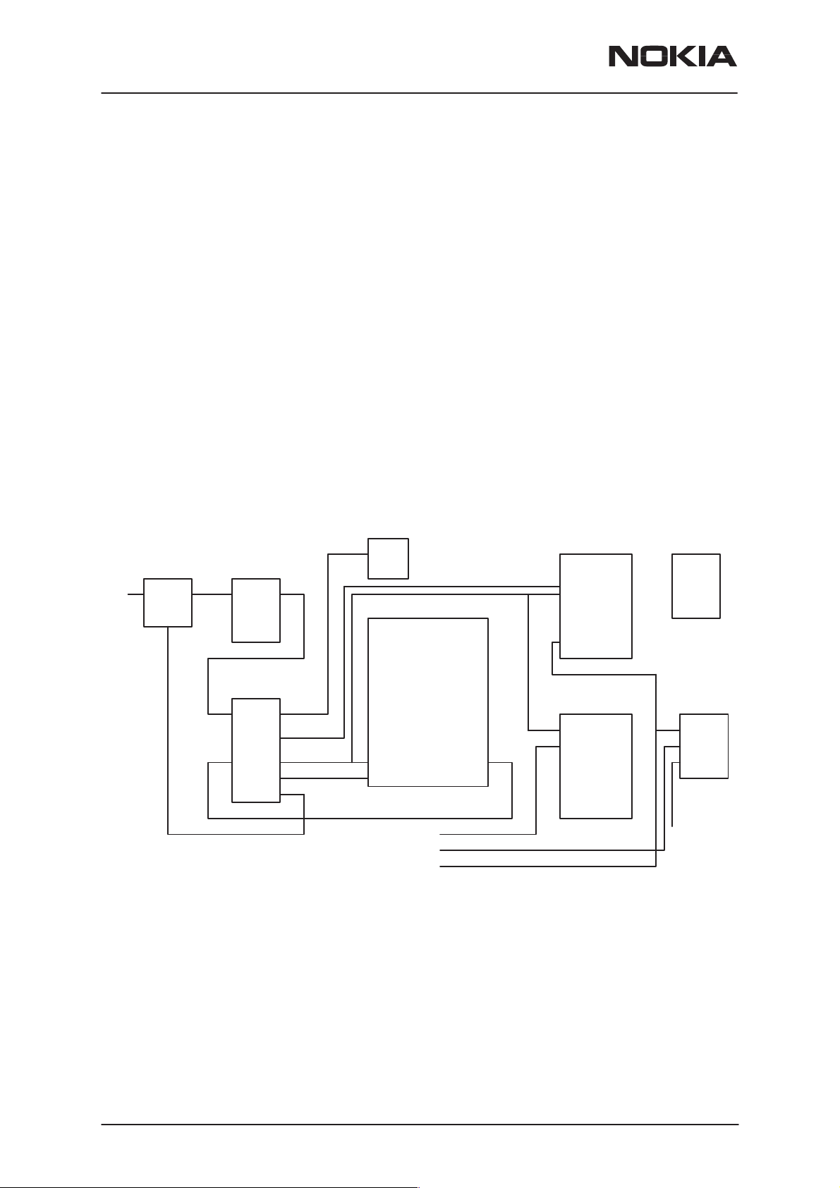
INF
An infrared transceiver module is implemented as an alternative to a
cable between the phone and a PC. See the figure below:
VBB
R358
R357
V351
6 Vcc
Shut down
4 RxD
Anode 1
IR MODULE
N350
3 TxD
C355R355
7 SC
FBUSRXD
MAD1
D202
B1DSPGenPIO(3)
A11
A12FBUSTXD
R209
IRDAEN >
2.5 V
Enable
1,7
VBB
Dual bus
R212
buffer
D350
26
V350
R354
53
C353
C352
VBAT
C350
R350
R352
Page 28
8
V200
X100
SYSTEM CONNECTOR12 13
The infrared transceiver module is a stand alone component capable of
infrared transmitting and receiving by transforming signals transmitted in
Nokia Mobile Phones Ltd.
Issue 1 10/00
Page 43

PAMS Technical Documentation
infrared light from and to electrical data pulses running in the two wire
asyncronous databus. IR databus is the same as used for FBUS data
transferring. Thus FBUS Tx and Rx lines must be turned to IR mode. The
IR mode can be selected from user interface.
The module is activated with the IRDAEN signal by MAD, which supplies
power to the IR module (N350) and enables supply current for IR leds.
The IR datalines are connected to MAD accessory interface AccIf via
FBUS. The RX and TX lines are separated from FBUS by 3–state buffer
(D350), when the IR–module is switched off. The AccIf performs pulse
encoding and shaping for transmitted data and detection and decoding
for received data pulses.
The data is transferred over IR link using serial FBUS data at speeds 9.6,
19.2, 38.4, 56.6 or 115.2 kbits/s, which leads to maximum troughput of
92.160 kbits/s. The used IR module complies with the IrDA SIR specification (Infra Red Data Association).
Following figure gives an example of IR transmission pulses. In IR transmission a light pulse correspondes to 0–bit and a ”dark pulse” correspondes to 1–bit.
NSW-5
System Module UT5U
IR TX
UART TX
startbit stopbit1 0100110
The FBUS cannot be used for external accessory communication, when
the infrared mode is selected. Infrared communication reserves the FBUS
completely.
User Interface
The Display Module is connected to engine board via X300. It contains
LCD and LCD LEDs, power switch, and speaker pads.
constant pulse
TM23A (N300), a.k.a. UISWITCH, is an integrated switch IC for UI purposes. It includes control switch for buzzer and vibra, LED (display & keyboard) control and two current sinks for LEDs.
Issue 1 10/00
Nokia Mobile Phones Ltd.
Page 29
Page 44

NSW-5
System Module UT5U
UISWITCH main features
– two adjustable constant current sinks for keyboard and LCD LEDs
– LED ON/OFF control
– buzzer ON/OFF control
– FET switch for buzzer current
– vibra ON/OFFcontrol (no internal vibrator in NSW–5)
– FET switch for vibra current
– thermal shutdown
– power down function for optimum current consumption
– package TSSOP20 because of low height requirement
PAMS Technical Documentation
Page 30
Nokia Mobile Phones Ltd.
Issue 1 10/00
Page 45

PAMS Technical Documentation
RF Module
Technical Summary
The RF module converts the signal received by the antenna to a
baseband signal and vice versa.
It consists of a conventional superheterodyne receiver and a transmitter
for each band and also two frequency synthesizers for the required
mixing.
The RF module includes one integrated circuit, the EROTUS a BiCMOS
ASIC.
The dual–band RF–module is capable for seamless operation between
800 MHz and 1900 MHz bands. In practise this means capability to
cross–band hand–offs and maho–measurements.
NSW-5
System Module UT5U
The EROTUS includes:
– Limiter amplifier for the analog receiver
– An AGC amplifier for the digital receiver
– A receiver mixer for the 450kHz down conversion
– PLLs for the 1GHz UHF and VHF synthesizers
– IQ–modulators for the transmitter
– A power control circuit for the transmitter and the AGC amplifier
The power amplifiers (PAs) are GaAs HBT MMICs. They comprise two
800 MHz and three 1900 MHz amplifier stages with input and interstage
matching.
The LNA MMICs include:
– A LNA for each band with a step AGC
– Down converters for the receiver
– A prescaler for the LO buffer
On the next page is a graphical presentation of the used Frequency Plan.
RF Frequency Plan
Intermediate frequencies of the RX are the same in all operation modes.
RX/TX LO and TX IF modulator frequencies are different in TDMA800
and TDMA1900 operation modes. See figure below for details.
Issue 1 10/00
Nokia Mobile Phones Ltd.
Page 31
Page 46

NSW-5
System Module UT5U
PAMS Technical Documentation
1930.08–1989.96 MHz
869.04–893.97 MHz
2046.24–2106.18 MHz
LO 1
PLLLO 3
1850.01–1909.95 MHz
824.01–848.97 MHz
NOTE!
Frequencies in
TDMA1900
are printed in italics
mode
985.20–1010.16 MHz
196.23 MHz
161.19 MHz
LO 2
392.46 MHz
322.38 MHz
1st IF
116.19 MHz
PLL
f
f/2
PLL
VCTCXO
19.44 MHz
2nd IF
450 kHz
116.64 MHz
EROTUS
IF2 A–mode
450 kHz
IF2 D–mode
450 kHz
2f
f
58.32 MHz
3f
f
RFC 19.44 MHz
DC Characteristics
Power Distribution Diagram
There are two options for power distribution. 1st option is a dual band
phone, which is presented in fig. 2. Current consumptions in the diagrams are only suggestive.
Page 32
Nokia Mobile Phones Ltd.
Issue 1 10/00
Page 47

PAMS Technical Documentation
NSW-5
System Module UT5U
RFCEN
SPWR1
TXPWR1
RXPWR1
SPWR2
(via serial bus)
TXPWR3
TXP1
VR7_bias
DUAL BAND OPERA TION
VR1
VREF
VR2
V5V
VR6
VR5
VR4
VR3
CCONT
VR7
VRBB BASEBAND
2 mA
19.44 MHz
8 mA
30 mA
1 mA
4 mA
3 mA
15 mA
Enable
3 mA
55 mA
VCTCXO
3* Multiplier
UHF–
VCO
2 mA
COBBA_D
(Analog)
Detector
VRS
IF1 –
amp.
VHF
VCO
TQ UHF
LO buffer
TX mixer
TDMA800
TX PA bias
TDMA800
TX driver
TDMA800
2 mA
2 mA
6 mA
10 mA
5 mA (peak)
2 mA
1 mA
35 mA
26 mA/ 5.6 mA
1 mA
doubler
VHF
presc.
Bias
UHF
presc.
& PLL
Phase
Digital
supply
Power
control
Modulator
Digital m.
RX IF– parts
Analog m.
IF– parts
Limiter
EROTUS
Control
block
TX PA
TDMA800
Freq.
det.
SDATA
SCLK
SENA1
VBATT
RXPWR2
RXPWR3
SPWR3
TXP2
TXPWR2
Current consumption in different operation modes can be seen in the
table next page.
Issue 1 10/00
Enable
VR8
VR9
19 mA
30 mA
RX FRONT
END TDMA800
RX FRONT
END TDMA1900
VR10
VR11
35 mA
VR12
TX mixer
TDMA1900
Enable
Nokia Mobile Phones Ltd.
10 mA
10 mA
Enable
3 mA
65 mA
4 mA
TX PA
TDMA1900
2GHz VCO
2GHz PLL
TX PA bias
TDMA 1900
TX driver
TDMA1900
TQ UHF
LO buffer
5 mA
Page 33
Page 48

NSW-5
System Module UT5U
PAMS Technical Documentation
800 MHz
Ext.
Standby
[mA]
VR1 9.0 / 0.0 9.0 9.0 9.0 / 0.0 9.0 19.0 / 0.0 19.0
VR2 16.0 / 0.0 16.0 16.0 16.0 / 0.0 16.0 0.0 0.0
VR3 0.0 0.0 23.0 0.0 13.0 0.0 8.0
VR4 11.6 / 0.0 11.6 11.6 32 / 0.0 12.8* 32 / 0.0 12.8*
VR5 0.0 0.0 37.0 0.0 13.0 ** 0.0 13.0 **
VR6 2.0 / 0.1 2.0 32.0 *** 2.0 / 0.1 32.0 *** 2.0 / 0.1 32.0 ***
VR7 0.0 0.0 58.0 0.0 19.2 ’ 0.0 0.0
VR8 19.0 / 0.0 19.0 19.0 19.0 / 0.0 7.6 ’’ 0.0 0.0
VR9 0.0 0.0 0.0 0.0 0.0 30.0 / 0.0 12.0 ’’’
VR10 0.0 0.0 0.0 0.0 0.0 10.0 / 0.0 10.0
VR11 0.0 0.0 0.0 0.0 0.0 0.0 22.5^
VR12 0.0 0.0 0.0 0.0 0.0 0.0 12.9^^
V5V 5.0 / 0.0 5.0 5.0 5.0 / 0.0 5.0 5.0 / 0.0 5.0
Total 62.6 / 0.1 62.6 210.6 83.0 / 0.1 127.6 98.0 / 0.1 147.2
800 MHz
Analog
Control
Channel
[mA]
800 MHz
Analog
Traffic
Channel
[mA]
800 MHz
Digital
Control
Channel
[mA]
800 MHz
Digital
Traffic
Channel
[mA]
1900 MHz
Digital
Control
Channel
[mA]
1900 MHz
Digital
Traffic
Channel
[mA]
Regulators
Most of the RF voltage regulation functions are located in the regulator IC
CCONT. It has 8 separate regulators with power on/off controls (see fig
2). Regulator VR6 is used only for the COBBA_D IC and the rest of the
regulators VR1–VR7 are reserved for the RF blocks. VR7_bias controls
the 800MHz PA bias to boost better efficiency in analog mode and at
power levels 6 to 10 in digital mode. V5V voltage is used for the PLL
charge pump supply. In dual band phone there is a need for 5 additional
regulators, which are integrated in Penta regulator IC.
Receiver
DAMPS800 RX
NOTES:* Mean value (ON/OFF=8/20ms), peak current 32.0 mA
** Mean value (ON/OFF=7/20ms), peak current 37.0 mA
*** Cobba_D mean current consumption estimated to be 30 mA
’ Mean value (ON/OFF=6.6/20ms), peak current 180.0 mA
’’ Mean value (ON/OFF=8/20ms), peak current 10.0 mA
’’’ Mean value (ON/OFF=8/20ms), peak current 15.0 mA when AGC2=1
^ Mean value (ON/OFF=6.6/20ms), peak current 68.0 mA
^^ Mean value (ON/OFF=6.6/20ms), peak current 39.0 mA
Page 34
The receiver is a double conversion receiver. Most of the RX functions
are integrated in two ICs, namely receiver front end and EROTUS. Receiver front end contains a LNA and the 1st mixer. Analog and digital IF–
parts are integrated in the EROTUS.
Nokia Mobile Phones Ltd.
Issue 1 10/00
Page 49

PAMS Technical Documentation
The received RF signal from the antenna is fed through a duplex filter to
the receiver unit. The signal is amplified by a low noise preamplifier. In
digital mode the gain of the amplifier is controlled by the AGC2 control
line. The nominal gain of 15 – 20 dB is reduced in the strong signal
condition about 14 – 19 dB (in digital mode). After the preamplifier the
signal is filtered with a SAW RF filter. The filter rejects spurious signals
coming from the antenna and spurious emissions coming from the mixer
and IF parts.
The filtered RF–signal is downconverted by an active mixer. The frequency of the first IF is 116.19 MHz. The first local signal is generated in
the UHF synthesizer. The IF signal is fed through a SAW IF–filter. The
filter rejects intermodulating signals and the second IF image signal. The
filtered 1st IF is fed to the receiver section of the integrated RF circuit
EROTUS, which has separate IF paths for analog and digital modes of
operation.
In digital mode the IF1 signal is amplified by an AGC amplifier, which has
a gain control range of 57 dB. The gain is controlled by an analog signal
with AGC1–line. The amplified IF signal is down converted to a second
IF in the mixer of EROTUS. The second local signal is the 6th overtone of
the 19.44 MHz VCTCXO. LO frequency multiplier is implemented in two
stages. First multiplication by 3 is done with a EROTUS multiplier with an
external trap and the second multiplication by 2 is done in the integrated
doubler in EROTUS.
NSW-5
System Module UT5U
The second IF frequency is 450 kHz. The second IF is filtered by two ceramic filters. The filter rejects signals on the adjacent channels. The filtered second IF is fed back to EROTUS, where it is amplified and fed
balanced out to COBBA_D via IF2D lines.
In analog mode the filtered and amplified IF1 signal is fed to a mixer. This
mixer has been optimized for low current consumption. After this the
mixer down converted signal is fed through the same IF2 filter as in digital
mode and finally it is amplified in the limiter amplifier. The limited IF2 signal is fed via balanced IF2A lines to COBBA_D, which has a digital FM–
detector. The limiter amplifier produces also a RSSI voltage for analog
mode field strength indication.
TDMA 1900 RX
On 1900 MHz band the receiver operates only in digital mode. There is a
separate front end for this band. IF–parts are common for both bands.
Operation of the receiver is similar to digital mode operation on 800 MHz
band.
Frequency Synthesizers
The stable frequency reference for the synthesizers and base band circuits is a voltage controlled temperature compensated crystal oscillator
VCTCXO. Frequency of the oscillator is 19.44 MHz. It is controlled by an
Issue 1 10/00
Nokia Mobile Phones Ltd.
Page 35
Page 50

NSW-5
System Module UT5U
AFC voltage, which is generated in the base band circuits. In digital mode
operation, the receiver is locked to base station frequency by AFC. Next
to detector diode, there is a sensor for temperature measurement. Voltage RFTEMP from this sensor is fed to baseband for A/D conversion.
This information of the RF PA–block temperature is used as input for
compensation algorithms.
The ON/OFF switching of the VCTCXO is controlled by the sleep clock in
the baseband via RFCEN. Other parts of the synthesizer section are 1
GHz VCO, 2 GHz VCO, VHF VCO, PLL for 2 GHz VCO and PLL sections
of the EROTUS IC.
DAMPS 800 operation
1GHz UHF synthesizer generates the down conversion injection for the
receiver and the up conversion injection for the transmitter. UHF frequency is 985.20 ... 1010.16 MHz, depending on the channel which is
used. 1GHz UHF VCO is a module. The PLL circuit is dual PLL, common
for both UHF and VHF synthesizers. These PLLs are included in the
EROTUS IC.
PAMS Technical Documentation
LO signal for the 2nd RX mixer is multiplied from the VCTCXO frequency
as described above.
VHF synthesizer is running only on digital or analog traffic channel.
322.38 MHz signal (divided by 2 in EROTUS) is used as a LO signal in
the I/Q modulator of the transmitter chain.
TDMA 1900 operation
2 GHz VCO with external PLL circuit generates 2046.24 ... 2106.18 MHz
injection signals for 1st RX mixer and TX upconverter.
VHF synthesizer is running only on digital traffic channel. Operating frequency 392.46 MHz is fed to EROTUS modulator, where it is divided by 2
and used as modulator LO signal.
Transmitter
DAMPS800 TX
The TX intermediate frequency is modulated by an I/Q modulator contained in the transmitter section of EROTUS IC. The TX I and TXQ signals are generated in the COBBA_D interface circuit and they are fed differentially to the modulator.
Page 36
Intermediate frequency level at the modulator output is controlled by
power control.
The output signal from EROTUS modulator is filtered to reduce harmonics and RX–band noise. The final TX signal is achieved by mixing the
UHF VCO signal and the modulated TX intermediate signal in an active
Nokia Mobile Phones Ltd.
Issue 1 10/00
Page 51

PAMS Technical Documentation
mixer. After the mixing TX signal is amplified by a driver stage. From
driver stage the signal is fed trough the TX filter to PA MMIC.
The PA amplifies the TX signal by 28–32 dB. Amplified TX signal is filtered in the duplex filter. Then signal is fed to the antenna, where the
maximum output level is typically 480 mW.
The power control loop controls the gain of the EROTUS gain control
stage. The power detector consists of a directional coupler and a diode
rectifier. The output voltage of the detector is compared to TXC voltage in
EROTUS. The power control signal (TXC), comes from the RF interface
circuit, COBBA_D. TXP signal sets driver power down to ensure off–burst
level requirements.
False transmission indication is used to protect transmitter against false
transmission caused by component failure. Protection circuit is in EROTUS. The level for TXF is set by internal resistor values in EROTUS.
TDMA1900 TX
NSW-5
System Module UT5U
See 800 MHz digital mode transmitter.
DAMPS800/TDMA1900 operation
Supply voltages in different modes of operation
800
MHz
Ext.
Stadby
VR1 ON/OFF ON ON ON/OFF ON ON/OFF ON
VR2 ON/OFF ON ON ON/OFF ON ON/OFF* ON/OFF*
VR3 OFF OFF ON OFF ON OFF OFF
VR4 ON/OFF ON ON ON/OFF ON/OFF ON/OFF ON/OFF
VR5 OFF OFF ON OFF ON/OFF OFF ON/OFF
VR7 OFF OFF ON OFF ON/OFF OFF OFF
VR8 ON/OFF ON ON ON/OFF ON/OFF OFF OFF
VR9 OFF OFF OFF OFF OFF ON/OFF ON/OFF
VR10 OFF OFF OFF ON/OFF* ON/OFF* ON ON
VR11 OFF OFF OFF OFF OFF OFF ON/OFF
VR12 OFF OFF OFF OFF OFF OFF ON/OFF
V5V ON/OFF ON ON ON/OFF ON ON/OFF ON
800
MHz
Analog
Control
Channel
NOTE: * ON during interband MAHO
800
MHz
Analog
Traffic
Channel
800
MHz
Digital
Control
Channel
800
MHz
Digital
Traffic
Channel
1900
MHz
Digital
Control
Channel
1900
MHz
Digital
Traffic
Channel
Software Compensations
Power Levels (TXC) vs. Temperature
Because of wide temperature range, it is neccessary to compensate the
effect of temperature on the output power. To monitor this environment
Issue 1 10/00
Nokia Mobile Phones Ltd.
Page 37
Page 52

NSW-5
System Module UT5U
change, temperature measurement is done by using NTC resistor. A
Factor table is used for temperature compensation. The table values are
defined without factory measurements. Temperature is measured and
right compensation value is added to TXC–value. Requirement for compensation update is for every 1 minutes or after every 5°C of temperature
change. This means that the PL2 output power is reduced linearily 0.5dB
when temperature inside the phone rises from +55°C to+80°C.
Power Levels (TXC) vs. Channel
Duplexer frequency response ripple is compensated by software. Power
levels are calibrated on four channels in production. Values for channels
between these tuned channels are calculated using linear interpolation.
Power levels vs. Battery Voltage
To extend battery duration in digital mode, the output power is decreased
linearily from level 2 to –0.5 dB when battery voltage drops below 3.3V.
PAMS Technical Documentation
TX Power Up/Down Ramps
Transmitter output power up/down ramps are controlled by SW. A special
ramp tables are used for that. Requirement is for nine different ramps in
digital mode for both operating bands. Separate ramps are used in power
up and power down ramps.
Modulator Output Level
Maximum Pout level values:
–20dBm for power levels 2...5
–24dBm for power level 6
–28dBm for power level 7
–20dBm for power levels 8...10
Digital Mode RSSI
Digital mode RSSI vs. input signal is calibrated in production, but RSSI
vs. RSSI vs. channel are compensated by software.
RF Block Specifications
Receiver
DAMPS 800MHz RX Front End
Receiver front end is integrated in the IC. It has a RF low noise amplifier
with a gain step and an active mixer. RX interstage filter is a SAW filter.
Page 38
Nokia Mobile Phones Ltd.
Issue 1 10/00
Page 53

PAMS Technical Documentation
NSW-5
System Module UT5U
Parameter Min Typ/
Gain, (LNA + filter + mixer) 19 21 24 dB
Gain, LNA gain disabled 4 dB
Gain step 14 17 dB
Supply Voltage 2.7 2.8 2.9 V
Supply Current (LNA + Mixer) 17 22 mA
TDMA 1900MHz RX Front End
Receiver front end is integrated in the IC. It has RF amplifier with a gain
step and an active mixer. RX interstage filter is a dielectric filter.
Parameter Min Typ/
Gain, (LNA + filter + mixer) 19 21 23 dB
Gain, LNA gain disabled 4 dB
Gain step 14 17 dB
Supply Voltage 2.7 2.8 2.9 V
Max Unit
Nom
Max Unit
Nom
Supply Current (LNA + Mixer) 28 33 mA
1st IF Amplifier
The 1st IF filter is a SAW filter. The function of the filter is to provide attenuation for the intermodulating signals
Analog IF parts
Analog mode IF–parts are included in EROTUS. Functional blocks: IF1
amplifier, a 2x–multiplier for LO signal, a mixer and a limiter amplifier
with RSSI. Specifications for analog mode IF–parts are in table 5. IF2
filter is a double 450 kHz ceramic filter.
Supply voltage 2.7 2.8 2.9 V
IF1 amp + mixer current cons. 6.5 8 mA
6x freq. multipl. current cons. 1.8 2 mA
Limiter + RSSI current cons. 1.4 2.5 mA
Parameter Min Typ/
Nom
Max Unit
(+0.6 mA in d–mode)
Power up time 3.5 ms
RF input impedance single end 3.5 4//tbd 5 kohm//pF
RF input frequency range 116.19 MHz
Noise figure, IF1 amp + mixer 8 dB, RF = 116 MHz
Issue 1 10/00
Nokia Mobile Phones Ltd.
Page 39
Page 54

NSW-5
System Module UT5U
PAMS Technical Documentation
MinParameter
UnitMaxTyp/
Nom
Conversion gain @
Rl=1.5kohm
Conversion gain variation TBD dB, temp -30...+85°C
3rd order input intercept point 20 mV
Mixer output frequency range 450 kHz
Mixer out to limiter in isolation 70 dB, @ 450 kHz
Limiter input frequency 450 kHz
Limiter input limiting range 30 uV
Limiter output voltage 0.3 V
Limiter output resistive load 10 kΩ
Limiter output capacitive load 5 pF
RSSI dynamic range 65 70 dB
RSSI starting level @ LIMIN1 30 60 uVrms
RSSI voltage slope 5 10 mV/dB
RSSI voltage range 0.1 1.5 V
RSSI output capacitive load 50 pF
25 33 dB
rms
rms
pp
RSSI output resistive load 500 kΩ
Freq. multiplier input frequency 19.44 MHz
Input signal spurious levels –10 dBc, (19.44 MHz
Input signal level 600 1000 mV
Digital IF parts
The digital IF–parts of EROTUS comprise AGC Amplifer with 57 dB control range, a mixer and a buffer amplifier for the last IF.
Supply voltage 2.7 2.8 2.9 V
Current consumption 25.2 34.5 mA
RF input frequency range 116.19 MHz
Local frequency (6x19.44 MHz) 116.64 MHz
IF frequency 450 kHz
Max voltage gain, AGC + mixer 47 dB
Min voltage gain, AGC + mixer –10 dB
Parameter Min Typ/
Nom
spurs)
pp
Max Unit
Page 40
Noise figure @ max gain 8 dB
Control voltage for min gain 0.7 V
Control voltage for max gain 1.4 1.45 V
AGC gain control slope TBD 90 TBD dB/V
Nokia Mobile Phones Ltd.
Issue 1 10/00
Page 55

PAMS Technical Documentation
NSW-5
System Module UT5U
Mixer output 1dB compr. point 0.8 V
Gain of the last IF buffer 34 36 38 dB, single ended
Max IF2–buffer output level 1.4 V
IF2–buffer output impedance 300 ohm, single ended
Transmitter
RF Characteristics of the transmitter:
TX frequency range 824.01...848.97 MHz 1850.01...1909.95 MHz
Type
Intermediate frequency 161.19 MHz 196.23 MHz
Nominal power on highest power level 0.48W (26.8 dBm) 0.355W (25.5 dBm)
Power control range 65 dB
Maximum rms error vector 12.5 %
MinParameter
UnitMaxTyp/
Nom
pp
pp
Item DAMPS TDMA1900
Upconversion
Synthesizers
Output levels
2G UHF synthesizer to Lo buffer
1G UHF synthesizer to TX mixer
VHF synthesizer to EROTUS
VCTCXO 19.44 MHz
Parameter Min Typ/
Nom
level
resistive load
parallel capacitance
level
impedance
level
resistive load
parallel capacitance
level
resistive load
parallel capacitance
–7
–2
100
1k
600
1k
tbd
tbd
tbd
tbd
Max Unit
dBm
Ω
pF
dBm
Ω
mV
pp
Ω
pF
mV
pp
Ω
20
pF
Issue 1 10/00
Nokia Mobile Phones Ltd.
Page 41
Page 56

NSW-5
System Module UT5U
PAMS Technical Documentation
VCTCXO 19.44 MHz to BB
level
resistive load
parallel capacitance
VCTCXO
3 * fo level
fo and 2xfo level
harmonic supression
resistive load
parallel capacitance
MinParameter
200
50
–25
–25
Nom
10k
tbd
5k
tbd
mV
Ω
pF
100 mV
dBc
dBc
Ω
pF
UnitMaxTyp/
pp
pp
Page 42
Nokia Mobile Phones Ltd.
Issue 1 10/00
Page 57

PAMS Technical Documentation
serial
)
)
RF/BB interface signals
NSW-5
System Module UT5U
CCONT (baseband) control signals are included in table below.
control signals are printed in italics.
Signal
name
VBAT battery RF
VREF CCONT Erotus
VR1 CCONT
VR2 CCONT
VR3 CCONT
From/
Control
/
RFCEN
/
SPWR1
/
SPWR2
(via
To Parameter Min Typ Max Unit Function
2V8
regul.
Erotus,
VCTCXO,
2GHz
PLL
Erotus,
UHF
VCO1
VHF–
VCO,
LO–buff,
TX mixer
These
Voltage 3.1 3.6 5.3 V Supply voltage for
discrete 2V8 regulators in dual band
phone
Voltage during TX 3.0 3.6 5.0 V
Current 1200 mA
Voltage 1.485 1.50 1.522 V EROTUS reference
voltage
Current 10 uA
Voltage 2.7 2.8 2.9 V Supply for VCTCXO,
and Erotus VHF
prescaler, VCO and
bias,
2 GHz PLL
Current, tdma 800 3.0 7 9 mA
Current, tdma1900 3.0 17 19 mA
Voltage 2.7 2.8 2.9 V Supply voltage for
tdma 800 UHF VCO
and prescaler
Current, tdma800 14 16 20 mA
Current, tdma1900 off mA
Voltage 2.7 2.8 2.9 V Supply for VHF VCO,
LO buffer, tdma800
TX mixer and TXF
bus
VR4 CCONT
/
RXPWR
1
VR5 CCONT
/
TXPWR
1
VR7 CCONT
TXP1
Erotus,
VCTCXO
IF1–amp
Erotus,
TX pwr
control
TX PA
Issue 1 10/00
Current, tdma800 20 24 30 mA
Current, tdma1900 4 9 12 mA
Voltage 2.7 2.8 2.9 V Supply for Erotus
IF–parts, IF1–amp.,
VCTCXO multiplier
Current, anal.RX 10 12 15 mA
Current, digi.RX 30 32 34 mA
Voltage 2.7 2.8 2.9 V Supply for Erotus
modulator, TX pwr
control
Current, TX–mode 33 37 41 mA
Voltage 2.7 2.88 2.95 V TX PA bias and TX
driver regulator
enable
Current, tdma800 55 60 mA
Nokia Mobile Phones Ltd.
Page 43
Page 58

NSW-5
System Module UT5U
PAMS Technical Documentation
Signal
name
VR7_bias CCONT
V5V CCONT/EROTUS
RFTEMP RF CCONT Voltage 0 1.5 V RF temperature sen-
AFC Cob-
Control
/
VMODE
RFCEN
ba_D
RF
800MhZ
PA bias
control for
analog
mode
VCTCXO
Logic high ”1” tbd V 800MHz PA bias volt-
Voltage 4.8 5.0 5.2 V Erotus and discrete
Current 3.0 5.0 mA
Voltage Min 0.05 1.2 2.25 V Automatic frequency
Resolution 11 bits
Load resistance
(dynamic)
Load resistance
(DC)
10 kΩ
110 kΩ
FunctionUnitMaxTypMinParameterToFrom/
age is increased to
improve analog mode
efficiency
synthesizer phase det
sor (47 k NTC to
GND)
control signal for
VCTCXO. When
DAC is switched
OFF AFC output is in
high–Z mode
AGC1 Cob-
ba_D
AGC2 MAD
(CTID
AGC2,
genpio)
IF2AP/
IF2AN
ERO-
TUS
EROTUS
RX LNA
Cobba_D
Voltage Min 0.7 1.40 V Digital mode receiver
gain control.
DSP
Load resistance 10 kΩ
Load capacitance 10 pF
Resolution 10 bits
Timing inaccuracy 8 us
Logic high ”1” 2.0 V LNA gain switch.
Polarity: 0=reduced
1=normal
DSP
Logic low ”0” 0.5 V
Sink/source curr. 10 100 uA
Load capacitance 10 pF
Timing inaccuracy 8 us
IF2 frequency 450 kHz Differential IF2–sig-
nal from limiter to
DEMO detector in
Cobba_D
Output level, 0.2 Vpp
Load resistance 10 kΩ
Load capacitance 5 pF
Page 44
Nokia Mobile Phones Ltd.
Issue 1 10/00
Page 59

PAMS Technical Documentation
g
MUX
NSW-5
System Module UT5U
Signal
name
IF2DP/
IF2DN
RFC VCTCXOCobba_D
RFCEN
RSSI ERO-
RXPWR2 MAD
RXPWR3 MAD
Control
ERO-
TUS
MAD
(CTID,
RFCEN
TUS
(CTID,
DSP
FTC)
(CTID,
DSP
FTC)
MUX
Cobba_D
(via ERO-
CCONT,
Cobba_D,
RF block
)
2V8 regu-
CCONT
RF block
regulator
RF block
regulator
TUS
lator
2V8
2V8
FunctionUnitMaxTypMinParameterToFrom/
IF2 frequency 450 kHz Differential IF2–sig-
nal
to RX A/D–converter,
PGA = 0 dB
Output level 170 1400
Source imp. 300 Ω
Frequency 19.44 MHz High stability clock
Signal amplitude 0.2 1.0 Vpp
Load resistance 10 kΩ
Load capacitance 5 pF
Logic high ”1” 2.0 V Supply voltage VR1
Logic low ”0” 0.5 V Supply voltage VR1
Current 100 uA
timing inaccuracy 50 us
Voltage 0.1 1.5 V Analog mode
Load resistance 0.5 MΩ
Load capacitance 50 pF
Logic high ”1” 2.0 V Supply voltage VR8
Logic low ”0” 0.5 V Supply voltage VR8
Current 100 uA DSP
timing inaccuracy 30 us
Logic high ”1” 2.0 V Supply voltage VR9
Logic low ”0” 0.5 V Supply voltage VR9
Current 100 uA DSP
timing inaccuracy 30 us
mVpp
signal for the logic
circuits
ON, RFC enable, RF
block 2V8 regulator
(PENTA) enable
OFF, RFC disable,
RF block 2V8 regula-
tor (PENTA) disable
MCU, DSP
field strength
indicator voltage
Digital mode
ON
OFF
ON
OFF
Issue 1 10/00
Nokia Mobile Phones Ltd.
Page 45
Page 60

NSW-5
SCLK
)
PLL
SDATA
)
PLL
SENA1
)
enable
SENA2
)
tdma1900
er
S
controlled
otus
controlled via Erotus
System Module UT5U
PAMS Technical Documentation
Signal
name
SCLK MAD
SDATA MAD
SENA1 MAD
SENA2 MAD
Control
(SCU,
(SCU,
(SCU,
(SCU,
EROTUS,
UHF
tdma1900
EROTUS,
UHF
tdma1900
EROTUS
UHF
PLL
Logic high ”1” 2 V
Logic low ”0” 0.8 V
Load resistance 50 k
Load capacitance 20 pF
Data rate freq. 1.62 MHz
Logic high ”1” 2.0 V
Logic low ”0” 0.8 V
Load resistance 50 k
Load capacitance 20 pF
Timing accuracy 20 us
Logic high ”1” 2.0 V
Logic low ”0” 0.8 V
Load resistance 50 k
Load capacitance 20 pF
Logic high ”1” 2.0 V
Logic low ”0” 0.8 V
Load resistance 50 k
Load capacitance 20 pF
FunctionUnitMaxTypMinParameterToFrom/
Synthesizer
and control clock
Synthesizer
and control data
Synthesizer
and Erotus control
TDMA1900 UHF
synthesizer enable
SPWR3 Cob-
ba_D
TXA MAD EROTUS
(MFI,
TXA
)
TXC Cob-
ba_D
TXF ERO-
TU
RF
2v8
regul.
EROTUS
MAD
Logic high ”1” 2.0 V Supply voltage VR10
ON
Logic low ”0” 0.5 V Supply voltage VR10
OFF
Current 100 uA
timing inaccuracy 200 us
Logic high ”1” 2.0 V Power control loop
Logic low ”0” 0.5 V Power control loop
Load resistance 10 k
Load capacitance 20 pF
Timing inaccuracy 10 us
Voltage Min value
Max value
Load resistance 10 k
Load capacitance 10 pF
Number of bits 10
Logic high ”1” 2.0 3.0 V
Logic low ”0” 0 0.5 V
Load capacitance 10 pF
0.12
2.27
0.15
2.30
0.18
2.33
DSP
mode during tx burst
mode during ramp
up/down
DSP
V
Makes transmitter
power ramps and
sets transmitter pow-
level
False transmission
indicator, function
register
via Er
Page 46
Nokia Mobile Phones Ltd.
Issue 1 10/00
Page 61

PAMS Technical Documentation
TXPWR1
TXPWR1
(
,
(MFI,
TX PA
mode
NSW-5
System Module UT5U
Signal
name
TXIP/
TXIN
TXQP/
TXQN
TXLX1 MAD
Control
Cob-
ba_D
Cob-
ba_D
(CTID,
TXLX
)
EROTUS
EROTUS
RF
tdma800
FunctionUnitMaxTypMinParameterToFrom/
Differential voltage
swing
Common mode v.
(digital mode)
Load resistance
(differential)
Differential voltage
swing
Common mode v.
(digital mode)
Load resistance
(differential)
Logic high ”1” 2.1 V High power level
Logic low ”0” 0 0.6 V Low power level
Sink/source curr. 8.0 mA
Load capacitance 10 pF
0.62 0.82 V
0.8 V
10 MW
0.62 0.82 V
0.8 V
10 MW
pp
pp
Differential in–phase
TX baseband signal
for the RF modulator.
Differential quadrature phase TX baseband signal for the
RF modulator.
mode for power detector
mode for power detector
Timing tied to
TXLX2 MAD
(TXLX2,
DSPGen-
Pio(6)
TXP2 MAD
MFI
TXP
)
)
RF
tdma1900
Penta
reg,
TX driver,
,
in
tdma1900
mode
Timing inaccuracy 8 us
Logic high ”1” 2.1 V High power level
Logic low ”0” 0 0.6 V Low power level
Sink/source curr. 8.0 mA
Load capacitance 10 pF
Timing inaccuracy 8 us
Logic high ”1” 2.0 V Supply voltage VR11
Logic low ”0” 0.5 V Supply voltage VR1 1
Current 100 uA
Load capacitance 10 pF
Timing inaccuracy 10 us
DSP
mode for power detector
mode for power detector
Timing tied to
DSP
ON
OFF
DSP
Issue 1 10/00
Nokia Mobile Phones Ltd.
Page 47
Page 62

NSW-5
TXPWR
(CTID
5)
tx mixer
System Module UT5U
PAMS Technical Documentation
Signal
name
TXPWR1
TXPWR2 MAD
TXPWR3 MAD RF
Control
MAD
(CTID,
TXPWR
1
)
BENA
(gen-
pio
,
)
CCONT,
EROTUS
RF
2v8
regul.
800MHz
enable
FunctionUnitMaxTypMinParameterToFrom/
Logic high ”1” 2.0 V Supply voltage VR5
ON, TX power control enable
Logic low ”0” 0.5 V Supply voltage VR5
OFF, TX power control disable
Current 50 uA
Timing inaccuracy 8 us
Logic high ”1” 2.0 V Supply voltage VR12
Logic low ”0” 0.5 V Supply voltage VR12
Current 50 uA
Timing inaccuracy 8 us
Logic high ”1” 2.0 V Mixer enabled
Logic low ”0” 0.5 V Mixer disabled
Current 2 mA
Timing inaccuracy 8 us
DSP
ON
OFF
DSP
DSP
Page 48
Nokia Mobile Phones Ltd.
Issue 1 10/00
Page 63

NSW-5
PAMS Technical Documentation
System Module UT5U
Parts Lists
Engine Module UT5U (0201142)
(EDMS V 13.1)
ITEM CODE DESCRIPTION VALUE TYPE
R100 1430764 Chip resistor 3.3 k 5 % 0.063 W 0402
R101 1430758 Chip resistor 1.5 k 5 % 0.063 W 0402
R150 1620019 Res network 0w06 2x10k j 0404
R152 1430804 Chip resistor 100 k 5 % 0.063 W 0402
R153 1419007 Chip resistor 0.22 0.5W 1210
R154 1430826 Chip resistor 680 k 5 % 0.063 W 0402
R155 1430770 Chip resistor 4.7 k 5 % 0.063 W 0402
R156 1430710 Chip resistor 22 5 % 0.063 W 0402
R159 1430762 Chip resistor 2.2 k 5 % 0.063 W 0402
R161 1620025 Res network 0w06 2x100k j 0404
R163 1620019 Res network 0w06 2x10k j 0404 0404
R164 1430778 Chip resistor 10 k 5 % 0.063 W 0402
R165 1430796 Chip resistor 47 k 5 % 0.063 W 0402
R166 1825005 Chip varistor vwm14v vc30v 0805 0805
R167 1430325 Chip resistor 2.2 M 5 % 0.063 W 0603
R169 1430796 Chip resistor 47 k 5 % 0.063 W 0402
R200 1620025 Res network 0w06 2x100k j 0404 0404
R201 1620025 Res network 0w06 2x100k j 0404 0404
R205 1620031 Res network 0w06 2x1k0 j 0404 0404
R208 1430744 Chip resistor 470 5 % 0.063 W 0402
R209 1430812 Chip resistor 220 k 5 % 0.063 W 0402
R210 1430770 Chip resistor 4.7 k 5 % 0.063 W 0402
R211 1430804 Chip resistor 100 k 5 % 0.063 W 0402
R212 1430796 Chip resistor 47 k 5 % 0.063 W 0402
R250 1430812 Chip resistor 220 k 5 % 0.063 W 0402
R251 1620103 Res network 0w06 2x22r j 0404 0404
R252 1430754 Chip resistor 1.0 k 5 % 0.063 W 0402
R256 1620025 Res network 0w06 2x100k j 0404 0404
R258 1430718 Chip resistor 47 5 % 0.063 W 0402
R259 1430804 Chip resistor 100 k 5 % 0.063 W 0402
R260 1620023 Res network 0w06 2x47k j 0404 0404
R261 1430742 Chip resistor 390 5 % 0.063 W 0402
R264 1430718 Chip resistor 47 5 % 0.063 W 0402
R265 1430762 Chip resistor 2.2 k 5 % 0.063 W 0402
R266 1620105 Res network 0w06 2x2k2 j 0404 0404
R268 1430812 Chip resistor 220 k 5 % 0.063 W 0402
R270 1430812 Chip resistor 220 k 5 % 0.063 W 0402
R273 1430826 Chip resistor 680 k 5 % 0.063 W 0402
R274 1430830 Chip resistor 1.0 M 5 % 0.063 W 0402
R275 1620031 Res network 0w06 2x1k0 j 0404 0404
R307 1430732 Chip resistor 180 5 % 0.063 W 0402
Issue 1 10/00
Nokia Mobile Phones Ltd.
Page 49
Page 64

NSW-5
System Module UT5U
R308 1430732 Chip resistor 180 5 % 0.063 W 0402
R309 1620101 Res network 0w06 2x470r j 0404 0404
R311 1430732 Chip resistor 180 5 % 0.063 W 0402
R312 1430744 Chip resistor 470 5 % 0.063 W 0402
R313 1620019 Res network 0w06 2x10k j 0404 0404
R314 1430758 Chip resistor 1.5 k 5 % 0.063 W 0402
R315 1430754 Chip resistor 1.0 k 5 % 0.063 W 0402
R316 1620031 Res network 0w06 2x1k0 j 0404 0404
R317 1620031 Res network 0w06 2x1k0 j 0404 0404
R318 1430788 Chip resistor 22 k 5 % 0.063 W 0402
R320 1620031 Res network 0w06 2x1k0 j 0404 0404
R322 1620031 Res network 0w06 2x1k0 j 0404 0404
R350 1620117 Res network 0w06 2x5r6 j 0404 0404
R352 1620117 Res network 0w06 2x5r6 j 0404 0404
R354 1430788 Chip resistor 22 k 5 % 0.063 W 0402
R355 1430754 Chip resistor 1.0 k 5 % 0.063 W 0402
R357 1430762 Chip resistor 2.2 k 5 % 0.063 W 0402
R358 1430804 Chip resistor 100 k 5 % 0.063 W 0402
R702 1430700 Chip resistor 10 5 % 0.063 W 0402
R709 1430788 Chip resistor 22 k 5 % 0.063 W 0402
R721 1430718 Chip resistor 47 5 % 0.063 W 0402
R725 1430710 Chip resistor 22 5 % 0.063 W 0402
R744 1430758 Chip resistor 1.5 k 5 % 0.063 W 0402
R751 1430790 Chip resistor 27 k 5 % 0.063 W 0402
R752 1430744 Chip resistor 470 5 % 0.063 W 0402
R756 1430790 Chip resistor 27 k 5 % 0.063 W 0402
R758 1430778 Chip resistor 10 k 5 % 0.063 W 0402
R760 1620047 Res network 0w03 4x4k7 j 0804 0804
R761 1430830 Chip resistor 1.0 M 5 % 0.063 W 0402
R762 1430851 Chip resistor 15 k 2 % 0.063 W 0402
R763 1430758 Chip resistor 1.5 k 5 % 0.063 W 0402
R764 1430744 Chip resistor 470 5 % 0.063 W 0402
R765 1430744 Chip resistor 470 5 % 0.063 W 0402
R767 1430758 Chip resistor 1.5 k 5 % 0.063 W 0402
R768 1430778 Chip resistor 10 k 5 % 0.063 W 0402
R770 1430700 Chip resistor 10 5 % 0.063 W 0402
R771 1430700 Chip resistor 10 5 % 0.063 W 0402
R774 1430764 Chip resistor 3.3 k 5 % 0.063 W 0402
R775 1430804 Chip resistor 100 k 5 % 0.063 W 0402
R779 1430762 Chip resistor 2.2 k 5 % 0.063 W 0402
R781 1430762 Chip resistor 2.2 k 5 % 0.063 W 0402
R782 1430762 Chip resistor 2.2 k 5 % 0.063 W 0402
R788 1430744 Chip resistor 470 5 % 0.063 W 0402
R789 1430744 Chip resistor 470 5 % 0.063 W 0402
R795 1430726 Chip resistor 100 5 % 0.063 W 0402
R796 1430700 Chip resistor 10 5 % 0.063 W 0402
R798 1430778 Chip resistor 10 k 5 % 0.063 W 0402
R822 1430700 Chip resistor 10 5 % 0.063 W 0402
PAMS Technical Documentation
Page 50
Nokia Mobile Phones Ltd.
Issue 1 10/00
Page 65

NSW-5
PAMS Technical Documentation
R830 1430792 Chip resistor 33 k 5 % 0.063 W 0402
R831 1430726 Chip resistor 100 5 % 0.063 W 0402
R832 1430754 Chip resistor 1.0 k 5 % 0.063 W 0402
R833 1430726 Chip resistor 100 5 % 0.063 W 0402
R850 1430778 Chip resistor 10 k 5 % 0.063 W 0402
R851 1430700 Chip resistor 10 5 % 0.063 W 0402
R860 1430778 Chip resistor 10 k 5 % 0.063 W 0402
R861 1430764 Chip resistor 3.3 k 5 % 0.063 W 0402
R862 1430726 Chip resistor 100 5 % 0.063 W 0402
R863 1430718 Chip resistor 47 5 % 0.063 W 0402
R864 1430700 Chip resistor 10 5 % 0.063 W 0402
R865 1430700 Chip resistor 10 5 % 0.063 W 0402
R880 1430700 Chip resistor 10 5 % 0.063 W 0402
R881 1430700 Chip resistor 10 5 % 0.063 W 0402
R883 1430754 Chip resistor 1.0 k 5 % 0.063 W 0402
R884 1430754 Chip resistor 1.0 k 5 % 0.063 W 0402
R886 1430772 Chip resistor 5.6 k 5 % 0.063 W 0402
R893 1430754 Chip resistor 1.0 k 5 % 0.063 W 0402
R901 1430718 Chip resistor 47 5 % 0.063 W 0402
R903 1430762 Chip resistor 2.2 k 5 % 0.063 W 0402
R904 1430758 Chip resistor 1.5 k 5 % 0.063 W 0402
R905 1430740 Chip resistor 330 5 % 0.063 W 0402
R911 1430726 Chip resistor 100 5 % 0.063 W 0402
R912 1430718 Chip resistor 47 5 % 0.063 W 0402
R928 1430732 Chip resistor 180 5 % 0.063 W 0402
R929 1430700 Chip resistor 10 5 % 0.063 W 0402
R933 1430718 Chip resistor 47 5 % 0.063 W 0402
R934 1620101 Res network 0w06 2x470r j 0404 0404
R936 1430754 Chip resistor 1.0 k 5 % 0.063 W 0402
R937 1430770 Chip resistor 4.7 k 5 % 0.063 W 0402
R938 1430778 Chip resistor 10 k 5 % 0.063 W 0402
R939 1430770 Chip resistor 4.7 k 5 % 0.063 W 0402
R940 1800659 NTC resistor 47 k 10 % 0.12 W 0805
R941 1430718 Chip resistor 47 5 % 0.063 W 0402
R942 1430764 Chip resistor 3.3 k 5 % 0.063 W 0402
R943 1430744 Chip resistor 470 5 % 0.063 W 0402
R944 1430770 Chip resistor 4.7 k 5 % 0.063 W 0402
R945 1430754 Chip resistor 1.0 k 5 % 0.063 W 0402
R960 1430770 Chip resistor 4.7 k 5 % 0.063 W 0402
R980 1430740 Chip resistor 330 5 % 0.063 W 0402
R984 1430730 Chip resistor 150 5 % 0.063 W 0402
C100 2320536 Ceramic cap. 10 p 5 % 50 V 0402
C101 2320536 Ceramic cap. 10 p 5 % 50 V 0402
C151 2320546 Ceramic cap. 27 p 5 % 50 V 0402
C153 2320586 Ceramic cap. 1.2 n 5 % 50 V 0402
C154 2320544 Ceramic cap. 22 p 5 % 50 V 0402
C155 2320530 Ceramic cap. 5.6 p 0.25 % 50 V 0402
C156 2320508 Ceramic cap. 1.0 p 0.25 % 50 V 0402
System Module UT5U
Issue 1 10/00
Nokia Mobile Phones Ltd.
Page 51
Page 66

NSW-5
System Module UT5U
C157 2320778 Ceramic cap. 10 n 10 % 16 V 0402
C158 2320481 Ceramic cap. 5R 1 u 10 % 0603
C159 2320481 Ceramic cap. 5R 1 u 10 % 0603
C160 2320481 Ceramic cap. 5R 1 u 10 % 0603
C161 2320481 Ceramic cap. 5R 1 u 10 % 0603
C162 2320481 Ceramic cap. 5R 1 u 10 % 0603
C163 2320481 Ceramic cap. 5R 1 u 10 % 0603
C164 2320481 Ceramic cap. 5R 1 u 10 % 0603
C166 2320481 Ceramic cap. 5R 1 u 10 % 0603
C169 2320481 Ceramic cap. 5R 1 u 10 % 0603
C170 2320805 Ceramic cap. 100 n 10 % 10 V 0402
C171 2320778 Ceramic cap. 10 n 10 % 16 V 0402
C172 2320778 Ceramic cap. 10 n 10 % 16 V 0402
C173 2320778 Ceramic cap. 10 n 10 % 16 V 0402
C174 2320778 Ceramic cap. 10 n 10 % 16 V 0402
C175 2310793 Ceramic cap. 2.2 u 10 % 10 V 0805
C176 2320481 Ceramic cap. 5R 1 u 10 % 0603
C177 2611727 Tantalum cap. 15 u 20 % 10 V
3.2x1.6x1.6
C179 2308792 Ceramic cap. 33 n 10 % 50 V 0805
C180 2320481 Ceramic cap. 5R 1 u 10 % 0603
C181 2320783 Ceramic cap. 33 n 10 % 10 V 0402
C182 2320744 Ceramic cap. 1.0 n 10 % 50 V 0402
C183 2611727 Tantalum cap. 15 u 20 % 10 V
3.2x1.6x1.6
C185 2611727 Tantalum cap. 15 u 20 % 10 V
3.2x1.6x1.6
C187 2320481 Ceramic cap. 5R 1 u 10 % 0603
C188 2610003 Tantalum cap. 10 u 20 % 10 V
3.2x1.6x1.6
C200 2320779 Ceramic cap. 100 n 10 % 16 V 0603
C201 2320481 Ceramic cap. 5R 1 u 10 % 0603
C202 2320779 Ceramic cap. 100 n 10 % 16 V 0603
C203 2320779 Ceramic cap. 100 n 10 % 16 V 0603
C207 2320778 Ceramic cap. 10 n 10 % 16 V 0402
C210 2320805 Ceramic cap. 100 n 10 % 10 V 0402
C214 2320805 Ceramic cap. 100 n 10 % 10 V 0402
C216 2320805 Ceramic cap. 100 n 10 % 10 V 0402
C217 2320481 Ceramic cap. 5R 1 u 10 % 0603
C218 2320481 Ceramic cap. 5R 1 u 10 % 0603
C219 2320805 Ceramic cap. 100 n 10 % 10 V 0402
C220 2320805 Ceramic cap. 100 n 10 % 10 V 0402
C221 2320805 Ceramic cap. 100 n 10 % 10 V 0402
C225 2320805 Ceramic cap. 100 n 10 % 10 V 0402
C250 2320526 Ceramic cap. 3.9 p 0.25 % 50 V 0402
C251 2320526 Ceramic cap. 3.9 p 0.25 % 50 V 0402
C252 2320536 Ceramic cap. 10 p 5 % 50 V 0402
C256 2320783 Ceramic cap. 33 n 10 % 10 V 0402
PAMS Technical Documentation
Page 52
Nokia Mobile Phones Ltd.
Issue 1 10/00
Page 67

NSW-5
PAMS Technical Documentation
C257 2320744 Ceramic cap. 1.0 n 10 % 50 V 0402
C258 2320805 Ceramic cap. 100 n 10 % 10 V 0402
C259 2310793 Ceramic cap. 2.2 u 10 % 10 V 0805
C260 2310793 Ceramic cap. 2.2 u 10 % 10 V 0805
C261 2320536 Ceramic cap. 10 p 5 % 50 V 0402
C262 2320560 Ceramic cap. 100 p 5 % 50 V 0402
C263 2320783 Ceramic cap. 33 n 10 % 10 V 0402
C264 2320783 Ceramic cap. 33 n 10 % 10 V 0402
C265 2320783 Ceramic cap. 33 n 10 % 10 V 0402
C266 2320783 Ceramic cap. 33 n 10 % 10 V 0402
C267 2320744 Ceramic cap. 1.0 n 10 % 50 V 0402
C270 2320536 Ceramic cap. 10 p 5 % 50 V 0402
C271 2320783 Ceramic cap. 33 n 10 % 10 V 0402
C272 2320805 Ceramic cap. 100 n 10 % 10 V 0402
C273 2320805 Ceramic cap. 100 n 10 % 10 V 0402
C274 2320805 Ceramic cap. 100 n 10 % 10 V 0402
C275 2320805 Ceramic cap. 100 n 10 % 10 V 0402
C276 2320546 Ceramic cap. 27 p 5 % 50 V 0402
C277 2320546 Ceramic cap. 27 p 5 % 50 V 0402
C278 2320783 Ceramic cap. 33 n 10 % 10 V 0402
C279 2320744 Ceramic cap. 1.0 n 10 % 50 V 0402
C280 2320546 Ceramic cap. 27 p 5 % 50 V 0402
C283 2320546 Ceramic cap. 27 p 5 % 50 V 0402
C285 2320783 Ceramic cap. 33 n 10 % 10 V 0402
C286 2320481 Ceramic cap. 5R 1 u 10 % 0603
C300 2320778 Ceramic cap. 10 n 10 % 16 V 0402
C301 2320778 Ceramic cap. 10 n 10 % 16 V 0402
C302 2320778 Ceramic cap. 10 n 10 % 16 V 0402
C304 2320546 Ceramic cap. 27 p 5 % 50 V 0402
C305 2320546 Ceramic cap. 27 p 5 % 50 V 0402
C306 2320778 Ceramic cap. 10 n 10 % 16 V 0402
C307 2320778 Ceramic cap. 10 n 10 % 16 V 0402
C350 2320546 Ceramic cap. 27 p 5 % 50 V 0402
C352 2320805 Ceramic cap. 100 n 10 % 10 V 0402
C353 2320546 Ceramic cap. 27 p 5 % 50 V 0402
C355 2320546 Ceramic cap. 27 p 5 % 50 V 0402
C357 2320779 Ceramic cap. 100 n 10 % 16 V 0603
C702 2320526 Ceramic cap. 3.9 p 0.25 % 50 V 0402
C703 2320546 Ceramic cap. 27 p 5 % 50 V 0402
C705 2320592 Ceramic cap. 2.2 n 5 % 50 V 0402
C706 2320546 Ceramic cap. 27 p 5 % 50 V 0402
C707 2320520 Ceramic cap. 2.2 p 0.25 % 50 V 0402
C708 2320524 Ceramic cap. 3.3 p 0.25 % 50 V 0402
C709 2320546 Ceramic cap. 27 p 5 % 50 V 0402
C710 2320778 Ceramic cap. 10 n 10 % 16 V 0402
C713 2320633 Ceramic cap. 220 p 5 % 25 V 0402
C715 2320604 Ceramic cap. 18 p 5 % 50 V 0402
C716 2320520 Ceramic cap. 2.2 p 0.25 % 50 V 0402
System Module UT5U
Issue 1 10/00
Nokia Mobile Phones Ltd.
Page 53
Page 68

NSW-5
System Module UT5U
C717 2320540 Ceramic cap. 15 p 5 % 50 V 0402
C719 2320760 Ceramic cap. 4.7 n 10 % 25 V 0402
C720 2320778 Ceramic cap. 10 n 10 % 16 V 0402
C721 2320560 Ceramic cap. 100 p 5 % 50 V 0402
C725 2320560 Ceramic cap. 100 p 5 % 50 V 0402
C726 2320560 Ceramic cap. 100 p 5 % 50 V 0402
C729 2320778 Ceramic cap. 10 n 10 % 16 V 0402
C733 2320536 Ceramic cap. 10 p 5 % 50 V 0402
C734 2320536 Ceramic cap. 10 p 5 % 50 V 0402
C735 2320524 Ceramic cap. 3.3 p 0.25 % 50 V 0402
C736 2320524 Ceramic cap. 3.3 p 0.25 % 50 V 0402
C739 2320520 Ceramic cap. 2.2 p 0.25 % 50 V 0402
C742 2320560 Ceramic cap. 100 p 5 % 50 V 0402
C743 2320552 Ceramic cap. 47 p 5 % 50 V 0402
C744 2320514 Ceramic cap. 1.2 p 0.25 % 50 V 0402
C745 2320617 Ceramic cap. 30 p 2 % 50 V 0402
C746 2320560 Ceramic cap. 100 p 5 % 50 V 0402
C748 2320778 Ceramic cap. 10 n 10 % 16 V 0402
C749 2320560 Ceramic cap. 100 p 5 % 50 V 0402
C750 2320744 Ceramic cap. 1.0 n 10 % 50 V 0402
C751 2320744 Ceramic cap. 1.0 n 10 % 50 V 0402
C755 2320728 Ceramic cap. 220 p 10 % 50 V 0402
C756 2320778 Ceramic cap. 10 n 10 % 16 V 0402
C757 2320576 Ceramic cap. 470 p 5 % 50 V 0402
C758 2320576 Ceramic cap. 470 p 5 % 50 V 0402
C759 2320131 Ceramic cap. 33 n 10 % 16 V 0603
C760 2320560 Ceramic cap. 100 p 5 % 50 V 0402
C761 2320760 Ceramic cap. 4.7 n 10 % 25 V 0402
C762 2320760 Ceramic cap. 4.7 n 10 % 25 V 0402
C763 2320760 Ceramic cap. 4.7 n 10 % 25 V 0402
C764 2320744 Ceramic cap. 1.0 n 10 % 50 V 0402
C765 2320744 Ceramic cap. 1.0 n 10 % 50 V 0402
C766 2320592 Ceramic cap. 2.2 n 5 % 50 V 0402
C767 2320760 Ceramic cap. 4.7 n 10 % 25 V 0402
C768 2320760 Ceramic cap. 4.7 n 10 % 25 V 0402
C769 2320760 Ceramic cap. 4.7 n 10 % 25 V 0402
C770 2320760 Ceramic cap. 4.7 n 10 % 25 V 0402
C772 2312401 Ceramic cap. 1.0 u 10 % 10 V 0805
C773 2320760 Ceramic cap. 4.7 n 10 % 25 V 0402
C779 2320778 Ceramic cap. 10 n 10 % 16 V 0402
C780 2320586 Ceramic cap. 1.2 n 5 % 50 V 0402
C781 2320778 Ceramic cap. 10 n 10 % 16 V 0402
C782 2312401 Ceramic cap. 1.0 u 10 % 10 V 0805
C783 2320778 Ceramic cap. 10 n 10 % 16 V 0402
C784 2320778 Ceramic cap. 10 n 10 % 16 V 0402
C785 2320546 Ceramic cap. 27 p 5 % 50 V 0402
C786 2320576 Ceramic cap. 470 p 5 % 50 V 0402
C787 2320576 Ceramic cap. 470 p 5 % 50 V 0402
PAMS Technical Documentation
Page 54
Nokia Mobile Phones Ltd.
Issue 1 10/00
Page 69

NSW-5
PAMS Technical Documentation
C788 2320560 Ceramic cap. 100 p 5 % 50 V 0402
C789 2320592 Ceramic cap. 2.2 n 5 % 50 V 0402
C790 2320779 Ceramic cap. 100 n 10 % 16 V 0603
C791 2320779 Ceramic cap. 100 n 10 % 16 V 0603
C792 2320779 Ceramic cap. 100 n 10 % 16 V 0603
C793 2320779 Ceramic cap. 100 n 10 % 16 V 0603
C794 2312401 Ceramic cap. 1.0 u 10 % 10 V 0805
C795 2320779 Ceramic cap. 100 n 10 % 16 V 0603
C796 2312401 Ceramic cap. 1.0 u 10 % 10 V 0805
C797 2312401 Ceramic cap. 1.0 u 10 % 10 V 0805
C798 2320779 Ceramic cap. 100 n 10 % 16 V 0603
C821 2320524 Ceramic cap. 3.3 p 0.25 % 50 V 0402
C822 2320546 Ceramic cap. 27 p 5 % 50 V 0402
C824 2312401 Ceramic cap. 1.0 u 10 % 10 V 0805
C825 2320560 Ceramic cap. 100 p 5 % 50 V 0402
C830 2320744 Ceramic cap. 1.0 n 10 % 50 V 0402
C831 2310248 Ceramic cap. 4.7 n 5 % 50 V 1206
C833 2320564 Ceramic cap. 150 p 5 % 50 V 0402
C834 2320564 Ceramic cap. 150 p 5 % 50 V 0402
C850 2320779 Ceramic cap. 100 n 10 % 16 V 0603
C851 2320744 Ceramic cap. 1.0 n 10 % 50 V 0402
C855 2312401 Ceramic cap. 1.0 u 10 % 10 V 0805
C860 2320744 Ceramic cap. 1.0 n 10 % 50 V 0402
C861 2420017 Ceramic cap. 18 n 5 % 16 V 1206
C864 2320564 Ceramic cap. 150 p 5 % 50 V 0402
C865 2320744 Ceramic cap. 1.0 n 10 % 50 V 0402
C866 2320564 Ceramic cap. 150 p 5 % 50 V 0402
C867 2312401 Ceramic cap. 1.0 u 10 % 10 V 0805
C868 2320560 Ceramic cap. 100 p 5 % 50 V 0402
C881 2320744 Ceramic cap. 1.0 n 10 % 50 V 0402
C882 2312401 Ceramic cap. 1.0 u 10 % 10 V 0805
C883 2320744 Ceramic cap. 1.0 n 10 % 50 V 0402
C885 2320744 Ceramic cap. 1.0 n 10 % 50 V 0402
C886 2320744 Ceramic cap. 1.0 n 10 % 50 V 0402
C887 2312401 Ceramic cap. 1.0 u 10 % 10 V 0805
C891 2320536 Ceramic cap. 10 p 5 % 50 V 0402
C898 2320560 Ceramic cap. 100 p 5 % 50 V 0402
C901 2320560 Ceramic cap. 100 p 5 % 50 V 0402
C903 2320560 Ceramic cap. 100 p 5 % 50 V 0402
C907 2320602 Ceramic cap. 4.7 p 0.25 % 50 V 0402
C908 2320560 Ceramic cap. 100 p 5 % 50 V 0402
C909 2320778 Ceramic cap. 10 n 10 % 16 V 0402
C910 2320546 Ceramic cap. 27 p 5 % 50 V 0402
C913 2320546 Ceramic cap. 27 p 5 % 50 V 0402
C914 2312401 Ceramic cap. 1.0 u 10 % 10 V 0805
C916 2320560 Ceramic cap. 100 p 5 % 50 V 0402
C918 2312401 Ceramic cap. 1.0 u 10 % 10 V 0805
C921 2320546 Ceramic cap. 27 p 5 % 50 V 0402
System Module UT5U
Issue 1 10/00
Nokia Mobile Phones Ltd.
Page 55
Page 70

NSW-5
System Module UT5U
C923 2320941 Ceramic cap. 10 V 0402
C924 2320744 Ceramic cap. 1.0 n 10 % 50 V 0402
C925 2320524 Ceramic cap. 3.3 p 0.25 % 50 V 0402
C927 2320560 Ceramic cap. 100 p 5 % 50 V 0402
C928 2320524 Ceramic cap. 3.3 p 0.25 % 50 V 0402
C931 2320522 Ceramic cap. 2.7 p 0.25 % 50 V 0402
C932 2320501 Ceramic cap. 50 V 0402
C934 2320546 Ceramic cap. 27 p 5 % 50 V 0402
C937 2320560 Ceramic cap. 100 p 5 % 50 V 0402
C938 2320536 Ceramic cap. 10 p 5 % 50 V 0402
C939 2320546 Ceramic cap. 27 p 5 % 50 V 0402
C941 2320560 Ceramic cap. 100 p 5 % 50 V 0402
C943 2320546 Ceramic cap. 27 p 5 % 50 V 0402
C949 2320522 Ceramic cap. 2.7 p 0.25 % 50 V 0402
C954 2320560 Ceramic cap. 100 p 5 % 50 V 0402
C955 2320536 Ceramic cap. 10 p 5 % 50 V 0402
C961 2320536 Ceramic cap. 10 p 5 % 50 V 0402
C962 2320552 Ceramic cap. 47 p 5 % 50 V 0402
C963 2320778 Ceramic cap. 10 n 10 % 16 V 0402
C965 2320560 Ceramic cap. 100 p 5 % 50 V 0402
C966 2320744 Ceramic cap. 1.0 n 10 % 50 V 0402
C968 2320921 Ceramic cap. 3.9 p 5 % 16 V 0402
C969 2320552 Ceramic cap. 47 p 5 % 50 V 0402
C970 2320530 Ceramic cap. 5.6 p 0.25 % 50 V 0402
C972 2320131 Ceramic cap. 33 n 10 % 16 V 0603
C981 2320530 Ceramic cap. 5.6 p 0.25 % 50 V 0402
C982 2320560 Ceramic cap. 100 p 5 % 50 V 0402
C984 2320540 Ceramic cap. 15 p 5 % 50 V 0402
C992 2320546 Ceramic cap. 27 p 5 % 50 V 0402
C999 2320903 Ceramic cap. 2.7 p 5 % 16 V 0402
L150 3203735 Ferrite bead 30r/100mhz 0805 0805
L701 3643007 Chip coil 18 n 5 % Q=30/250 MHz
0805
L702 3645063 Chip coil 270 n 5 % Q=48/250 MHz
0805
L703 3640045 Chip coil 10.Q n 5 % Q=55/750 MHz
0805
L705 3641622 Chip coil 220 n 5 % Q=30/100 MHz
0805
L721 3641521 Chip coil 6. Q n 5 % Q=50/250 MHz
0805
L723 3645147 Chip coil 100 n 5 % Q=12/100 MHz
0603
L724 3608407 Chip coil 470 n 5 % 1206
L740 3645231 Chip coil 39.Q n 5 % Q=40/250 MHz
0603
L741 3641620 Chip coil 180 n 5 % Q=35/100 MHz
0805
PAMS Technical Documentation
Page 56
Nokia Mobile Phones Ltd.
Issue 1 10/00
Page 71

NSW-5
PAMS Technical Documentation
L745 3645145 Chip coil 39.Q n 5 % Q=12/100 MHz
0603
L747 3645145 Chip coil 39.Q n 5 % Q=12/100 MHz
0603
L750 3641421 Chip coil 100 u 5 % Q=15/0.796M
1008
L761 3645029 Chip coil 1. Q u 10 % Q=45/10 MHz
0805
L762 3641626 Chip coil 220 n 2 % Q=50/250 MHz
0805
L868 3641421 Chip coil 100 u 5 % Q=15/0.796M
1008
L901 3645147 Chip coil 100 n 5 % Q=12/100 MHz
0603
L902 3645145 Chip coil 39.Q n 5 % Q=12/100 MHz
0603
L904 3645145 Chip coil 39.Q n 5 % Q=12/100 MHz
0603
L905 3645147 Chip coil 100 n 5 % Q=12/100 MHz
0603
L906 3643001 Chip coil 10 n 5 % Q=30/250 MHz
0805
L911 3640081 Dir.coupler 836.5+–12.5mhz 1206 1206
L930 3645129 Chip coil 18.Q n 5 % Q=8/100M 0603
L931 3645145 Chip coil 39.Q n 5 % Q=12/100 MHz
0603
L940 3645129 Chip coil 18.Q n 5 % Q=8/100M 0603
L941 3645117 Chip coil 5.–0 n Q=8/100M 0603
L951 3643011 Chip coil 22 n 5 % Q=40/250 MHz
0805
L960 3645155 Chip coil 2.–0 n Q=32/800M 0603
L961 3645145 Chip coil 39.Q n 5 % Q=12/100 MHz
0603
L962 3645145 Chip coil 39.Q n 5 % Q=12/100 MHz
0603
L964 3643001 Chip coil 10 n 5 % Q=30/250 MHz
0805
L965 3646001 Chip coil 3.–0 n Q=7/100M 0402
L966 4551003 Dir.coupler 1880+–30mhz 1 4DB
L975 3645147 Chip coil 100 n 5 % Q=12/100 MHz
0603
L977 3641572 Chip coil 22.Q n 5 % Q=45/250 MHz
0805
L978 3645155 Chip coil 2.–0 n Q=32/800M 0603
L980 3645145 Chip coil 39.Q n 5 % Q=12/100 MHz
0603
B150 4510243 Crystal 32.768 k +–20PPM 12.5PF
G820 4350185 Vco 985.2–1010.2mhz 2.8v tdma
System Module UT5U
Issue 1 10/00
Nokia Mobile Phones Ltd.
Page 57
Page 72

NSW-5
System Module UT5U
G850 4510249 VCTCXO 19.44 M +–2.5PPM 2.8V TDMA
G860 4350187 Vco 2046.2–2106.2mhz 2.8v TDMA
F150 5119019 SM, fuse f 1.5a 32v 0603
Z100 3640085 Filt 470nf 16v 0r03 2a 0805
Z250 3640035 Filt z>450r/100m 0r7max 0.2a 0603
Z251 3640035 Filt z>450r/100m 0r7max 0.2a 0603
Z252 3640035 Filt z>450r/100m 0r7max 0.2a 0603
Z701 4511125 Saw filter 881.5+–12.5 M/4DB 3X3
Z726 4511113 Saw filter 1960+–30 M/5DB 3X3
Z741 4511011 Saw filter 116.19+–0.015 M 9.3X5
Z750 4550085 Cer.filt 450+–11.5khz/8db 6.7x5.7
Z751 4550081 Cer.filt 450+–11.5khz/8db 6.7x5.7
Z900 4511031 Saw filter 161.2/196.2 M 5X5
Z901 4511123 Saw filter 836.5+–12.5 M /3.8DB 3X3
Z910 4512091 Dupl 824–849/869–894mhz 9.5x7.5
Z950 4511023 Saw filter 1880+–30 M /4.2DB 3X3
Z960 4512103 Dupl 1850–1910/1930–1990mhz 17x8
Z970 4550065 Dipl 824–894/1850–1990mhz 3.2x1.6
Z975 4511023 Saw filter 1880+–30 M /4.2DB 3X3
Z988 3640085 Filt 470nf 16v 0r03 2a 0805
V150 4210205 Transistor SOT23
V151 4110067 Schottky diode MBR0520L 20 V 0.5 A SOD123
V200 4113611 Emifilt/tvs emif01–10005w5 SOT353
V201 4113611 Emifilt/tvs emif01–10005w5 SOT353
V250 4210119 Transistor BC849CW npn 30 V 0.1 A
SOT323
V251 4211621 MosFet SOT363
V252 4113611 Emifilt/tvs emif01–10005w5 SOT353
V253 4113671 Tvs quad 6v1 esda6v1w5 SOT323–5
V254 4210052 Transistor DTC114EE npn RB V EM3
V255 4211641 MosFet SOT363
V256 4211641 MosFet SOT363
V300 4110601 Diode FAST SOD323
V302 4860005 Led Green 0603
V303 4860005 Led Green 0603
V304 4860005 Led Green 0603
V305 4860005 Led Green 0603
V306 4860005 Led Green 0603
V307 4860005 Led Green 0603
V350 4210052 Transistor DTC114EE npn RB V EM3
V351 4210102 Transistor BC858W pnp 30 V 100 mA
200MWSOT323
V723 4110911 Cap. diode MA2SV01 1/3 V SOD523
V901 4210043 Transistor DTC143ZE npn RB V EM3
V902 4210043 Transistor DTC143ZE npn RB V EM3
V929 4110055 Sch. diode x 2 BAT17–07 4 V SOT143
V930 4110055 Sch. diode x 2 BAT17–07 4 V SOT143
V932 4112469 Pindix2 bar64–07 200v 0.1a SOT143
PAMS Technical Documentation
Page 58
Nokia Mobile Phones Ltd.
Issue 1 10/00
Page 73

NSW-5
PAMS Technical Documentation
D100 4340761 IC, MCU MC33464N SOT23–5
D200 4340601 IC, SRAM CSP48
D201 4340597 IC, flash mem. UBGA48
D202 4370619 Mad1 v20 rom7 f731575 c07 UBGA144
D203 4340845 1xinverter 1.8v–5.5v(7sz04) sc70–5
D350 4340369 IC, dual bus buffer ssoTC7W126FU SSOP8
N150 4370719 Ccont 2m wfd163mg64t/8 lfbga8x8
N151 4370621 Chaps v2.0 u423v20g36t lbga6x6
N250 4370603 Cobba_d b06 twl91302ggv UBGA64
N300 4370433 Uiswitch sttm23av20t TSSOP20
N350 4860031 Tfdu4100 irda tx/rx>2.7v 115kbits 115KBITS
N701 4370063 Sc3918 tdma rec 869–894mhz QSOP16
N702 4340247 IC, regulator MC33765 2.8 V TSSOP16
N721 4370065 Sc3919 tdma rec 1930–1990 QSOP16
N750 4370183 Erotus wfd170ct64t tqfp64
N770 4340233 Mrfic0916 rf amp 2500mhz SOT143
N880 4340237 IC, PLL UMA1021M SSOP20
N900 4340171 IC, upconv 1.9ghz 3v souPC8106T SO6S
N902 4340577 IC, RF amp. 21DB/900MHZ SMM6
N903 4370311 Rf9103p1 pw amp 824–849 mhz
N951 4340577 IC, RF amp. 21DB/900MHZ SMM6
N960 4370313 Rf9111p1 pw amp 1850–1910mhz
N980 4340381 Mrfic1813 upconvgaas 1.9g TSSOP16
S318 5409077 SM, push button sw spst 15v 20ma
X100 5469061 SM, system conn 6af+3dc+mic+jack
X104 5469069 SM, batt conn 2pol spr p3.5 100V2A
X105 5469069 SM, batt conn 2pol spr p3.5 100V2A
X991 5429007 SM, coax conn m sw 50r 0.4–2ghz
A801 9517029 Shield assembly dmc01832
A802 9517030 Shield assy dmc01833
A803 9517029 Shield assembly dmc01832
9380753 Bar code label 27x6.5 dmd03311
9854264 PCB UT5 40.5X118.5X1.1 M8 4/PA
System Module UT5U
Issue 1 10/00
Nokia Mobile Phones Ltd.
Page 59
Page 74

NSW-5
System Module UT5U
PAMS Technical Documentation
This page intentionally left blank.
Page 60
Nokia Mobile Phones Ltd.
Issue 1 10/00
Page 75

PAMS Technical Documentation
NSW-5 Series Transceivers
Product Variants
Issue 1 10/2000 Nokia Mobile Phones Ltd.
Page 76

NSW-5
Product Variants
PAMS Technical Documentation
AMENDMENT RECORD SHEET
Amendment
Number
Date Inserted By Comments
Issue 1 10/00 OJuntune
Page 2
Nokia Mobile Phones Ltd.
Issue 1 10/2000
Page 77

PAMS Technical Documentation
Product Variants
CONTENTS
Variants of NSW–5 5. . . . . . . . . . . . . . . . . . . . . . . . . . . . . . . . . . . . . . . . . . . . . . .
Foreword 5. . . . . . . . . . . . . . . . . . . . . . . . . . . . . . . . . . . . . . . . . . . .
Modules 5. . . . . . . . . . . . . . . . . . . . . . . . . . . . . . . . . . . . . . . . . .
Exploded View of Transceiver NSW–5 6. . . . . . . . . . . . . . . .
Assembly Parts of NSW-5NX 8. . . . . . . . . . . . . . . . . . . . . . . .
NSW-5
Page No
Issue 1 10/2000
Nokia Mobile Phones Ltd.
Page 3
Page 78

NSW-5
Product Variants
PAMS Technical Documentation
This page intentionally left blank.
Page 4
Nokia Mobile Phones Ltd.
Issue 1 10/2000
Page 79

PAMS Technical Documentation
Variants of NSW–5
Foreword
This section of the service manual (Appendix) contains specific details for
the NSW-5 handportable telephone.
NOTE: The Service Manual is intended for use by qualified
service personnel only.
Modules
Name of module Type des. Material code Material code
Basic transceiver NSW–5 0501659
–System/RF module UT5U 0201142
– Software module ( Basic SW ) 0240823
– Mechanics assembly parts MNSW5 0261711
NSW-5
Product Variants
Issue 1 10/2000
Nokia Mobile Phones Ltd.
Page 5
Page 80

NSW-5
Product Variants
Exploded View of Transceiver NSW–5
I020
I009 I010
PAMS Technical Documentation
I018
I017
I013
I002
I001
I004
I003
I005
I007
I006
I008
I012
I011
I019
I016
I015
I014
Page 6
Nokia Mobile Phones Ltd.
Issue 1 10/2000
Page 81

PAMS Technical Documentation
Product Variants
Assembly Parts of NSW-5NX
ITEM Q’TY CODE DESCRIPTION VALUE, TYPE
I001 9497058 Slide cover assembly
I002 9497009 Slide assembly DMC01314
I003 (varia) Logo label
I004 9451486 A–cover assembly DMC01461
I005 9790342 Power Keymat/Speaker gasket DMC01487
I006 5200017 Slide sensor switch DMC01259
I007 5200013 Roller key assembly 10v 1ma
I008 9794014 Keymat module DMC01847
I009 5140067 Speaker + spring 103+–3DB
NSW-5
I010 9480401 Display assembly DMC01299
I010 0201142 Radio module UT5U
I012 5140123 Buzzer with gasket 100dB
I013 4700089 RTC battery polyacene 2.3 mAh 3.3V
I014 4 6290073 Screw M1.8x8 T6 remf. blk dmd03671
I015 9456335 B–cover assembly DMC01835
I016 2 6290079 Screw M1.8x11 T6 dmd04746
I017 9460299 Elastic plug DMD04645
I018 0660198 Antenna fxd 824–894/1850–1990mhz
I019 9451139 Dust Cap DMD02859
I020 9456920 Window assembly
Issue 1 10/2000
Nokia Mobile Phones Ltd.
Page 7
Page 82

NSW-5
Product Variants
PAMS Technical Documentation
This page intentionally left blank.
Page 8
Nokia Mobile Phones Ltd.
Issue 1 10/2000
Page 83

PAMS Technical Documentation
NSW-5 Series Transceivers
Service Software
Instructions
Issue 1 10/00 Nokia Mobile Phones Ltd.
Page 84

NSW-5
Service Software Instructions
AMENDMENT RECORD SHEET
PAMS Technical Documentation
Amendment
Number
Date Inserted By Comments
Issue 1 10/00 OJuntune
Page 2
Nokia Mobile Phones Ltd.
Issue 1 10/00
Page 85

PAMS Technical Documentation
Service Software Instructions
CONTENTS
Service Software 6. . . . . . . . . . . . . . . . . . . . . . . . . . . . . . . . . . . . . . . .
General 6. . . . . . . . . . . . . . . . . . . . . . . . . . . . . . . . . . . . . . . . . . . . .
Hardware requirements for Windows 3.1x 6. . . . . . . . . . .
Hardware requirements for Windows 95 6. . . . . . . . . . . .
Software Environment of the Support Modules 6. . . . . . . . .
Required Servicing Equipment 7. . . . . . . . . . . . . . . . . . . . . . .
Installation 8. . . . . . . . . . . . . . . . . . . . . . . . . . . . . . . . . . . . . . . .
Mechanical Connections 8. . . . . . . . . . . . . . . . . . . . . . . . . .
Installing the Software on PC Hard Disk 8. . . . . . . . . . . .
Common Properties of the User Interface 9. . . . . . . . . . . . . . . . . .
Login Dialog 9. . . . . . . . . . . . . . . . . . . . . . . . . . . . . . . . . . . . . . . . .
Main Window 10. . . . . . . . . . . . . . . . . . . . . . . . . . . . . . . . . . . . . . . .
Menu Bar 12. . . . . . . . . . . . . . . . . . . . . . . . . . . . . . . . . . . . . . . . . . . .
Product 12. . . . . . . . . . . . . . . . . . . . . . . . . . . . . . . . . . . . . . . . . . .
Configure 13. . . . . . . . . . . . . . . . . . . . . . . . . . . . . . . . . . . . . . . . .
Tuning 13. . . . . . . . . . . . . . . . . . . . . . . . . . . . . . . . . . . . . . . . . . . .
Testing 13. . . . . . . . . . . . . . . . . . . . . . . . . . . . . . . . . . . . . . . . . . . .
Software 14. . . . . . . . . . . . . . . . . . . . . . . . . . . . . . . . . . . . . . . . . .
Dealer 14. . . . . . . . . . . . . . . . . . . . . . . . . . . . . . . . . . . . . . . . . . . .
View 14. . . . . . . . . . . . . . . . . . . . . . . . . . . . . . . . . . . . . . . . . . . . . .
Help 15. . . . . . . . . . . . . . . . . . . . . . . . . . . . . . . . . . . . . . . . . . . . . .
Mouse Cursors 16. . . . . . . . . . . . . . . . . . . . . . . . . . . . . . . . . . . . . . .
Reserved Keys 16. . . . . . . . . . . . . . . . . . . . . . . . . . . . . . . . . . . . . . .
Short Cut Function Keys 16. . . . . . . . . . . . . . . . . . . . . . . . . . . .
Alt Hot Keys 16. . . . . . . . . . . . . . . . . . . . . . . . . . . . . . . . . . . . . . .
Ctrl Hot Keys 16. . . . . . . . . . . . . . . . . . . . . . . . . . . . . . . . . . . . . .
Shift Hot Keys 16. . . . . . . . . . . . . . . . . . . . . . . . . . . . . . . . . . . . .
Key Strokes 17. . . . . . . . . . . . . . . . . . . . . . . . . . . . . . . . . . . . . . .
Help Functions 19. . . . . . . . . . . . . . . . . . . . . . . . . . . . . . . . . . . . . . .
Dialog boxes 19. . . . . . . . . . . . . . . . . . . . . . . . . . . . . . . . . . . . . . . . .
Common Dialog boxes 19. . . . . . . . . . . . . . . . . . . . . . . . . . . . . .
Note Message Box 19. . . . . . . . . . . . . . . . . . . . . . . . . . . . . . .
Query Message Box 19. . . . . . . . . . . . . . . . . . . . . . . . . . . . .
Error Message Box 20. . . . . . . . . . . . . . . . . . . . . . . . . . . . . .
Custom Dialog boxes 21. . . . . . . . . . . . . . . . . . . . . . . . . . . . . . .
Buttons 21. . . . . . . . . . . . . . . . . . . . . . . . . . . . . . . . . . . . . . . . . . . . .
Reporting Status 22. . . . . . . . . . . . . . . . . . . . . . . . . . . . . . . . . . . . .
NSW-5 FEATURES 23. . . . . . . . . . . . . . . . . . . . . . . . . . . . . . . .
Menu bar 23. . . . . . . . . . . . . . . . . . . . . . . . . . . . . . . . . . . . . . . . .
Product 23. . . . . . . . . . . . . . . . . . . . . . . . . . . . . . . . . . . . . . . . . . .
New command 23. . . . . . . . . . . . . . . . . . . . . . . . . . . . . . . . . .
NSW-5
Page No
Issue 1 10/00
Nokia Mobile Phones Ltd.
Page 3
Page 86

NSW-5
Service Software Instructions
Open... command 23. . . . . . . . . . . . . . . . . . . . . . . . . . . . . . . .
Initialise... command 23. . . . . . . . . . . . . . . . . . . . . . . . . . . . .
Normal Mode 24. . . . . . . . . . . . . . . . . . . . . . . . . . . . . . . . . . . .
Local Mode 24. . . . . . . . . . . . . . . . . . . . . . . . . . . . . . . . . . . . .
Faultlog command 24. . . . . . . . . . . . . . . . . . . . . . . . . . . . . . .
Activate Faultlog 25. . . . . . . . . . . . . . . . . . . . . . . . . . . . . . . . .
Edit Faultlog 25. . . . . . . . . . . . . . . . . . . . . . . . . . . . . . . . . . . .
FastNAM command 25. . . . . . . . . . . . . . . . . . . . . . . . . . . . . .
Exit command 25. . . . . . . . . . . . . . . . . . . . . . . . . . . . . . . . . . .
Tuning 26. . . . . . . . . . . . . . . . . . . . . . . . . . . . . . . . . . . . . . . . . . . .
AFC... command 26. . . . . . . . . . . . . . . . . . . . . . . . . . . . . . . . .
VCTCXO... command 27. . . . . . . . . . . . . . . . . . . . . . . . . . . .
Tx Power... command 29. . . . . . . . . . . . . . . . . . . . . . . . . . . .
Tx I/Q... command 32. . . . . . . . . . . . . . . . . . . . . . . . . . . . . . .
RSSI Digital (AGC)... command 34. . . . . . . . . . . . . . . . . . . .
RSSI Analog... command 36. . . . . . . . . . . . . . . . . . . . . . . . .
Rx Audio... command 38. . . . . . . . . . . . . . . . . . . . . . . . . . . .
Tx Audio... command 39. . . . . . . . . . . . . . . . . . . . . . . . . . . . .
Charging... command 40. . . . . . . . . . . . . . . . . . . . . . . . . . . .
LCD... command 41. . . . . . . . . . . . . . . . . . . . . . . . . . . . . . . . .
Testing 42. . . . . . . . . . . . . . . . . . . . . . . . . . . . . . . . . . . . . . . . . . . .
RF Controls... command 42. . . . . . . . . . . . . . . . . . . . . . . . . .
Self Tests... command 45. . . . . . . . . . . . . . . . . . . . . . . . . . . .
ADC Readings... command 47. . . . . . . . . . . . . . . . . . . . . . .
Audio... command 48. . . . . . . . . . . . . . . . . . . . . . . . . . . . . . .
User Interface... command 50. . . . . . . . . . . . . . . . . . . . . . . .
IR Test... command 51. . . . . . . . . . . . . . . . . . . . . . . . . . . . . .
Software 52. . . . . . . . . . . . . . . . . . . . . . . . . . . . . . . . . . . . . . . . . .
Product Profile... command 52. . . . . . . . . . . . . . . . . . . . . . .
Set Default Values... command 54. . . . . . . . . . . . . . . . . . . .
Authority ID... command 55. . . . . . . . . . . . . . . . . . . . . . . . . .
Flash Phone... command 57. . . . . . . . . . . . . . . . . . . . . . . . .
A–key... command 58. . . . . . . . . . . . . . . . . . . . . . . . . . . . . . .
Dealer 59. . . . . . . . . . . . . . . . . . . . . . . . . . . . . . . . . . . . . . . . . . . .
User Settings... command 59. . . . . . . . . . . . . . . . . . . . . . . . .
Short Code Memory... command 61. . . . . . . . . . . . . . . . . . .
Calling cards... command 63. . . . . . . . . . . . . . . . . . . . . . . . .
System Service Feature codes... command 65. . . . . . . . .
Subscriber data programming... command 66. . . . . . . . . .
P/RSID programming... command 68. . . . . . . . . . . . . . . . . .
Intelligent Roaming Database... command 70. . . . . . . . . .
WAP Settings... command 73. . . . . . . . . . . . . . . . . . . . . . . .
User Data Transfer... command 75. . . . . . . . . . . . . . . . . . . .
View 76. . . . . . . . . . . . . . . . . . . . . . . . . . . . . . . . . . . . . . . . . . . . . .
Quick/RF Info... command 76. . . . . . . . . . . . . . . . . . . . . . . .
Phone Identity... command 77. . . . . . . . . . . . . . . . . . . . . . . .
PAMS Technical Documentation
Page 4
Nokia Mobile Phones Ltd.
Issue 1 10/00
Page 87

PAMS Technical Documentation
Appendix 1, Vocabulary 78. . . . . . . . . . . . . . . . . . . . . . . . . . . . . . . . . .
Service Software Instructions
NSW-5
Issue 1 10/00
Nokia Mobile Phones Ltd.
Page 5
Page 88

NSW-5
Service Software Instructions
Service Software
General
To run the After Sales SW, a parallel port software protection device
(PKD-1) has to be connected. TDF-4 box must connected to PC for
flashing purposes. The user can use PC-locals functions in modules for
testing NSW-5 mobile stations (MS). The test functions send test mes-
sages from PC to MS and receive results and show them in the PC dis-
play. The messages can be sent via M2BUS or FBUS.
Note: if this software is to be run on laptops, the power saving feature
MUST be switched off.
Hardware requirements for Windows 3.1x
The recommended minimum hardware standard to run Service Software
is any computer which is 386 33 MHz or greater with at least 4 MB of
memory and VGA type display (640 x 480). This assumes that only the
WinTesla with After Sales Support Modules is active, i.e. other Windows
packages are not running in the background.
PAMS Technical Documentation
Hardware requirements for Windows 95
The recommended minimum hardware standard to run Service Software
is any computer which has Pentium processor, memory 8 MB and meets
HW requirements recommended by Microsoft.
Software Environment of the Support Modules
The Service Software user interface is intended for the following environ-
ments: Microsoft Windows 3.1x (enhanced mode) and Windows 95envi-
ronment running in enhanced mode. Support for Microsoft NT may be
added, if required. Detailed information about Windows and application
usage can be found from the Microsoft Windows Version 3.1 Users Guide
chapter one (Windows Basics) and chapter two (Application Basics).
As an ordinary Windows application, the main idea in the user interface is
that selections are made with menus, push buttons and shortcut keys.
Selections can be done by using keyboard and/or mouse. There is always
a status bar displayed at the bottom of the main window which contains
information about current actions.
Page 6
Nokia Mobile Phones Ltd.
Issue 1 10/00
Page 89

PAMS Technical Documentation
Required Servicing Equipment
– Computer: At least IBM 80386 or compatible with one unused serial
port (COM1 or COM2)
mended
– Operating System: DOS Version 3.2 or later
– If PCLStart in use: DOS 6.22 and IBM 80486 or compatible
– Display: VGA type display (640 x 480)
– Service software on 3.5” disk (product code: 0775229)
– Software protection key PKD–1 (product code: 0750018)
– Service MBUS Cable DAU–9P (product code: 0730109)
– Audio cable ADS–1 (product code: 0730011)
– External Antenna Cable XRC–2 (product code 0730180)
NSW-5
Service Software Instructions
*)
, one parallel port (LPT1), hard disk recom-
– Modular T–adapter (product code: 4626134)
*)
Note: A number of PC’s of an older generation use the Intel, National Semiconductor, or United
Microelectronics IC 8250 as the serial port UART. This is a comparatively inefficient circuit for current
purposes and does not necessarily support the M2BUS adapter at 9600 baud. The newer UART’s
NS16450 and NS16550AF of National Semiconductor offer solutions for these problems.
Issue 1 10/00
Nokia Mobile Phones Ltd.
Page 7
Page 90

NSW-5
Service Software Instructions
Installation
Mechanical Connections
Caution: Make sure that you have switched off the PC and the printer
before making connections.
Caution: Do not connect the PKD–1 key to the serial port. You may
damage your PKD–1 !
The software controls the phone via a separate adapter connected to the
serial port of the PC, and to the telephone’s M2BUS (DAU–9S).
Attach the dongle PKD–1 to the parallel port 1 (25–pin female D–connector) of the PC. When connecting PKD–1 to the parallel port, be sure that
you insert the computer side of the PKD–1 to the PC (male side). If you
use a printer on parallel port 1, install the PKD–1 between the PC and
your printer cable.
PAMS Technical Documentation
The PKD–1 should not affect devices working with it. If some errors occur
(errors in printing are possible) please try printing without the PKD–1. If
printing is OK without the PKD–1 please contact your dealer. We will offer
you a new PKD–1 in exchange for your old one.
Installing the Software on PC Hard Disk
The program is delivered on a diskette and is copy protected with a
dongle PKD–1. It must be present in parallel port when using Service
software.
The program can also be installed on the hard disk, which is recommended to obtain a maximal data access rate.
Keep the original diskette safe to enable upgrading of the program !
If you plan to use PCL Start service software, you must install it before
installing Service software, see the PCL Start installation instructions.
To install the new Service software program, follow the steps below:
1. insert the new Service software diskette
into drive A: of your computer
Page 8
2. start Windows, and open File Manager
log into drive a:
3. start INSTALL.EXE and
install Service software to drive C:
Nokia Mobile Phones Ltd.
type
A:
type C: and press <Enter>
and press <Enter>
Issue 1 10/00
Page 91

PAMS Technical Documentation
Service Software Instructions
Common Properties of the User Interface
This chapter describes how the User Interface CLF must appear to the
user.
The User Interface MUST be capable of being driven without the use of a
mouse, as the service engineer rarely has space on the bench to use a
mouse.
Login Dialog
When the Service Software application is invoked, by clicking on the Service Software icon, the Login dialog box will be displayed on the screen.
NSW-5
Nokia logo and application name bitmap (–)
Application version static text (–)
Copyright notice static text (–)
Login Box edit box (–)
OK button (default key)
Issue 1 10/00
Displays Nokia logo and name of the application.
Contains the name and version of the application.
Copyright is informed as: “Nokia Mobile Phones (c)
1995–1999. All Rights Reserved”.
The user Login ID edit box, where the user enters his faultlog
user name. (See Faultlog User Guide)
The user name is stored in memory and the dialog box is
closed. When the dialog box is closed, the application starts.
Nokia Mobile Phones Ltd.
Page 9
Page 92

NSW-5
Service Software Instructions
Cancel button (ESC)
The Dialog box is closed and application is started, but the
Faultlog feature is disabled.
Help button (F1)
Activates the Windows Help application and displays context
sensitive Help.
Main Window
PAMS Technical Documentation
Page 10
Title bar
title bar
The
A title bar contains the following elements:
• Application Control–menu button
• Maximise button
• Minimise button
• Name of the application
• Restore button
is located at the top of the window.
Nokia Mobile Phones Ltd.
Issue 1 10/00
Page 93

PAMS Technical Documentation
The properties of these elements and their usage is described in Ref 3–
Microsoft Windows Version 3.1 Users Guide chapter one (Windows Basics) and chapter two (Application Basics).
Menu bar
NSW-5
Service Software Instructions
menu bar
The
tions. The menu bar is a dynamic element and is dependent on the
dongle type fitted, and whether a phone is connected.
Underlined characters in menu names and options indicates that the
menu selection can be done by pressing
tions can also be selected by activating menu bar with
key ) and using arrow–keys to highlight the desired menu. In that case,
selection is done by pressing
Menus can also be selected by using the mouse as described in Ref
3–Microsoft Windows Version 3.1 Users Guide
Status bar
The
status bar
window. The status bar contains information about the menu selections
and events.
The left area of the status bar describes the actions of menu items as the
user uses the arrow keys to navigate through menus.
The status bar texts are explained in detailed in each of command’s description.
The right areas of the status bar indicate which of the following keys are
latched down:
is below the title bar and contains all available menu selec-
Alt+ underlined character
Alt
– key ( or
Enter
.
is displayed at the bottom of the Service Software main
. Op-
F10
Indicator Description
USER Entered Login ID.
CAP The Caps Lock key is latched down.
NUM The Num Lock key is latched down.
SCRL The Scroll Lock key is latched down.
Tool bar
The
tool bar
this document.
is NOT defined and will not be implemented until specified by
Issue 1 10/00
Nokia Mobile Phones Ltd.
Page 11
Page 94

NSW-5
Service Software Instructions
Menu Bar
The Service Software package includes two menu bar configurations. The
first is an abbreviated version that contains the minimum number of menus that allows package configurations when a phone is NOT connected.
The second is described below:
The menu bar MUST only contain the following menus for the Service
Software package when a phone is connected:
roduct*
• P
onfigure*
• C
uning
• T
sting
• Te
• S
oftware
ealer
• D
PAMS Technical Documentation
Product
iew
• V
elp* (* – always displayed, even if no phone is connected).
• H
A menu is broken down into sections that are indicated with menu separators. Each sections identifies a logical difference from itself and other sections, i.e. between transmitter and receiver. Any items that are required to be
added to a menu lists will be added on the bottom of the appropriate menu
section list. If a new item is to be added which is common to two or more
phone types, then that menu item will become a common menu item.
The menu lists will use the Microsoft [...] symbol after an item name to indicate that selecting that item will NOT initiate an operation immediately,
i.e. a dialog box will be displayed for the user to select options or type in
data and press the OK button before the operation is performed.
The Product menu contains the following menu items:
ew Ctrl+R
• N
pen...
• O
Page 12
lose
• C
nitialise
• I
•F
aultlog
•Fast N
• Normal Mode F5
• Local Mode Shift+F5
• Activate Faultlog... F9
• Edit Faultlog...
AM (available only if fastNAM installed)
Nokia Mobile Phones Ltd.
Issue 1 10/00
Page 95

PAMS Technical Documentation
•Exit Alt+F4
Configure
The Configure menu contains the following items:
• O
ptions...
es...
• Bus
• D
irectories...
• F
aultlog...
NSW-5
Service Software Instructions
Tuning
• Fast N
The Tuning menu contains the following menu sections:
• A
• V
• M
• Tx
• Tx I/Q
• Rssi D
• Rssi An
• R
• T
• C
AM (active if installed)
FC..(Analog)
CTCXO...
odulator Output
Power...
...
igital (AGC)
alog
x Audio
x Audio
harging...
• L
Testing
The Testing menu contains the following sections:
• R
• S
• A
• Au
• U
Issue 1 10/00
CD...
F Controls...
elf Tests
DC Readings
dio
ser Interface
Nokia Mobile Phones Ltd.
Page 13
Page 96

NSW-5
Service Software Instructions
Software
The Software menu contains the following menu sections:
• P
roduct Profile...
PAMS Technical Documentation
Dealer
• Set Default V
• A
uthority ID...
• F
lash Phone...
• A key...
The Dealer menu contains the following menu sections:
• U
ser Settings...
• Short C
• Cal
ling cards...
• System Service F
• S
ubscriber data programming..
• P/R
SID programming...
ntelligent Roaming Database...
• I
• W
AP Settings
alues...
ode Memory...
eature codes..
View
• User D
The View menu contains the following sections:
• Q
• P
ata Transfer...
uick/RF Info...
hone Identity...
Page 14
Nokia Mobile Phones Ltd.
Issue 1 10/00
Page 97

PAMS Technical Documentation
Help
The Help menu contains the following menu items:
• I
ndex
• G
eneral Help
• U
sing Help
• A
bout WinTesla
NSW-5
Service Software Instructions
Issue 1 10/00
Nokia Mobile Phones Ltd.
Page 15
Page 98

NSW-5
Service Software Instructions
Mouse Cursors
The standards Windows pointer is used as the mouse cursor.
During time consuming tasks e.g. communication to phone, an hour glass
is shown informing the user that a task is in progress. The application
uses the hour glass cursor to inform user that the application has taken
the control and any actions from user will be ignored.
When a function is initiated, the hour glass is displayed and when the
function has finished the mouse pointer will return to normal.
Reserved Keys
The following Hot keys and Short Cut keys are reserved either as Microsoft standard keys or as part of the Common Look and Feel specified by
this document.
PAMS Technical Documentation
Short Cut Function Keys
Key Description Defined by
F1 Context Sensitive Help Microsoft
F5 Normal Mode NMP
Shift+F5 Local Mode NMP
F9 Activate Faultlog NMP
F10 Goto Menu Bar Microsoft
Ctrl+F4 Close Active Window Microsoft
Alt Hot Keys
Key Description Defined by
Alt+F4 Exit Active Application Microsoft
Alt+H Help Microsoft
Ctrl Hot Keys
Key Description Defined by
Ctrl+N File – New Microsoft
Ctrl+O F
Ctrl+P F
Ctrl+R P
Shift Hot Keys
Shift+F5 Local Mode NMP
Page 16
ile – Open Microsoft
ile – Print Microsoft
roduct – New NMP
Nokia Mobile Phones Ltd.
Issue 1 10/00
Page 99

PAMS Technical Documentation
Key Strokes
Key Description Defined by
Alt+P Product Menu NMP
NSW-5
Service Software Instructions
Alt+P,N N
Alt+P,O Open NMP
Alt+P,C Close NMP
Alt+P,I I
Alt+P,I,N Normal Mode NMP
Alt+P,I,L Local Mode NMP
Alt+P,F F
Alt+P,F,A Activate Faultlog NMP
Alt+P,F,E Edit Faultlog NMP
Alt+P,N Fast N
Alt+P,X Exit Application NMP
Alt+C Configure NMP
Alt+C,O O
Alt+C,S Buses NMP
Alt+C,D Directories NMP
ew NMP
nitialize Pop–up NMP
aultlog Pop–up NMP
AM NMP
ption NMP
Alt+C,F F
Alt+C,N Fast NAM NMP
Alt+C,G GPIB instruments (disabled) NMP
Alt+T Tuning Menu NMP
Alt+T,A A
Alt+T,V VCTCXO NMP
Alt+T,M Modulator Output NMP
Alt+T,X Tx
Alt+T,Q Tx I/Q NMP
Alt+T,D Rssi Digital (AGC) NMP
Alt+T,N Rssi An
Alt+T,R Rx Audio NMP
Alt+T,T Tx Audio NMP
Alt+T,C C
Alt+T,L LCD NMP
aultlog NMP
FC (Analog) NMP
Power NMP
alog NMP
harging NMP
Alt+E Te
Issue 1 10/00
sting Menu NMP
Nokia Mobile Phones Ltd.
Page 17
Page 100

NSW-5
Service Software Instructions
Alt+E,R RF Controls NMP
PAMS Technical Documentation
Alt+E,S S
Alt+E,A A
Alt+E,D Aud
Alt+E,U U
Alt+S S
Alt+S,P P
Alt+S,V Set Default V
Alt+S,A A
Alt+S,F F
Alt+D D
Alt+D,U U
Alt+D,C Short C
Alt+D,L Cal
Alt+D,V Set UI/DEV Default V
Alt+D,F System Service F
elf Tests NMP
DC Readings NMP
io NMP
ser Interface NMP
oftware Menu NMP
roduct Profile NMP
alues NMP
uthority ID NMP
lash Phone NMP
ealer Menu NMP
ser Settings NMP
ode Memory NMP
ling cards NMP
eature codes NMP
alues NMP
Alt+D,S S
Alt+D,R P/R
Alt+D,I I
Alt+D,D User D
Alt+V V
Alt+V,Q Q
Alt+V,P P
Alt+H H
Alt+H,I I
Alt+H,G G
Alt+H,U U
Alt+H,A A
ubscriber data programming NMP
SID programming NMP
ntelligent Roaming Database NMP
iew Menu NMP
uick/RF Info NMP
hone Identity NMP
elp Menu Microsoft
ndex Microsoft
eneral Help Microsoft
sing Help Microsoft
bout WinTesla NMP
ata Transfer NMP
Page 18
Nokia Mobile Phones Ltd.
Issue 1 10/00
 Loading...