

Page 1

PAMS Technical Documentation
NSE–5 Series Transceivers
Chapter 2
System Module
Issue 1 07/99
Page 2

NSE–5
System Module
Technical Documentation
Contents
System Connector 3 – 5. . . . . . . . . . . . . . . . . . . . . . . . . . . . . . . . . . . . . . . . . . . . . .
DC Connector 3 – 7. . . . . . . . . . . . . . . . . . . . . . . . . . . . . . . . . . . . . . . . . . . . . . . .
Slide Microphone 3 – 7. . . . . . . . . . . . . . . . . . . . . . . . . . . . . . . . . . . . . . . . . . . . .
Slide Connector 3 – 7. . . . . . . . . . . . . . . . . . . . . . . . . . . . . . . . . . . . . . . . . . . . . . .
Roller Interface 3 – 7. . . . . . . . . . . . . . . . . . . . . . . . . . . . . . . . . . . . . . . . . . . . . . .
Keys and Keymatrix 3 – 7. . . . . . . . . . . . . . . . . . . . . . . . . . . . . . . . . . . . . . . . . . .
Headset Connector 3 – 7. . . . . . . . . . . . . . . . . . . . . . . . . . . . . . . . . . . . . . . . . . . .
Battery Connector 3 – 14. . . . . . . . . . . . . . . . . . . . . . . . . . . . . . . . . . . . . . . . . . . . .
Vibra Alerting Device 3 – 14. . . . . . . . . . . . . . . . . . . . . . . . . . . . . . . . . . . . . . .
SIM Card Connector 3 – 15. . . . . . . . . . . . . . . . . . . . . . . . . . . . . . . . . . . . . . . . . . .
PAMS
Page No
Infrared Transceiver Module 3 – 16. . . . . . . . . . . . . . . . . . . . . . . . . . . . . . . . . . . .
Real Time Clock 3 – 17. . . . . . . . . . . . . . . . . . . . . . . . . . . . . . . . . . . . . . . . . . . . . .
Baseband Module 3 – 18. . . . . . . . . . . . . . . . . . . . . . . . . . . . . . . . . . . . . . . . . . . . . . .
Technical Summary 3 – 18. . . . . . . . . . . . . . . . . . . . . . . . . . . . . . . . . . . . . . . . . . .
Power Distribution 3 – 19. . . . . . . . . . . . . . . . . . . . . . . . . . . . . . . . . . . . . . . . . . . . .
Power Up 3 – 22. . . . . . . . . . . . . . . . . . . . . . . . . . . . . . . . . . . . . . . . . . . . . . . . . . . .
Power up with a charger 3 – 22. . . . . . . . . . . . . . . . . . . . . . . . . . . . . . . . . . . .
Power Up With The Power Switch (PWRONX) 3 – 22. . . . . . . . . . . . . . . . .
Power Up by RTC 3 – 23. . . . . . . . . . . . . . . . . . . . . . . . . . . . . . . . . . . . . . . . . .
Power Up by IBI 3 – 23. . . . . . . . . . . . . . . . . . . . . . . . . . . . . . . . . . . . . . . . . . . .
Acting Dead 3 – 23. . . . . . . . . . . . . . . . . . . . . . . . . . . . . . . . . . . . . . . . . . . . . . .
Active Mode 3 – 23. . . . . . . . . . . . . . . . . . . . . . . . . . . . . . . . . . . . . . . . . . . . . . .
Sleep Mode 3 – 24. . . . . . . . . . . . . . . . . . . . . . . . . . . . . . . . . . . . . . . . . . . . . . .
Battery charging 3 – 24. . . . . . . . . . . . . . . . . . . . . . . . . . . . . . . . . . . . . . . . . . .
Startup Charging 3 – 25. . . . . . . . . . . . . . . . . . . . . . . . . . . . . . . . . . . . . . . . . . .
Battery Overvoltage Protection 3 – 25. . . . . . . . . . . . . . . . . . . . . . . . . . . . . . .
Battery Removal During Charging 3 – 26. . . . . . . . . . . . . . . . . . . . . . . . . . . .
Different PWM Frequencies ( 1Hz and 32 Hz) 3 – 27. . . . . . . . . . . . . . . . . .
Battery Identification 3 – 28. . . . . . . . . . . . . . . . . . . . . . . . . . . . . . . . . . . . . . . .
Battery Temperature 3 – 29. . . . . . . . . . . . . . . . . . . . . . . . . . . . . . . . . . . . . . . .
Supply Voltage Regulators 3 – 30. . . . . . . . . . . . . . . . . . . . . . . . . . . . . . . . . .
Audio Control 3 – 31. . . . . . . . . . . . . . . . . . . . . . . . . . . . . . . . . . . . . . . . . . . . . . . . .
Internal Microphone and Earpiece 3 – 32. . . . . . . . . . . . . . . . . . . . . . . . . . . .
External Audio Connections 3 – 32. . . . . . . . . . . . . . . . . . . . . . . . . . . . . . . . .
Internal Audio Connections 3 – 34. . . . . . . . . . . . . . . . . . . . . . . . . . . . . . . . . .
Page 2 – 2
Issue 1 07/99
Page 3

PAMS
NSE–5
Technical Documentation
4–wire PCM Serial Interface 3 – 34. . . . . . . . . . . . . . . . . . . . . . . . . . . . . . . . .
Speech Processing 3 – 35. . . . . . . . . . . . . . . . . . . . . . . . . . . . . . . . . . . . . . . . .
Alert Signal Generation 3 – 35. . . . . . . . . . . . . . . . . . . . . . . . . . . . . . . . . . . . .
Digital Control 3 – 36. . . . . . . . . . . . . . . . . . . . . . . . . . . . . . . . . . . . . . . . . . . . . . . .
MAD2PR1 3 – 36. . . . . . . . . . . . . . . . . . . . . . . . . . . . . . . . . . . . . . . . . . . . . . . . .
MAD2PR1 pinout 3 – 37. . . . . . . . . . . . . . . . . . . . . . . . . . . . . . . . . . . . . . . . . . .
Memories 3 – 47. . . . . . . . . . . . . . . . . . . . . . . . . . . . . . . . . . . . . . . . . . . . . . . . . . . .
Program Memory 32MBit Flash 3 – 47. . . . . . . . . . . . . . . . . . . . . . . . . . . . . .
SRAM Memory 3 – 47. . . . . . . . . . . . . . . . . . . . . . . . . . . . . . . . . . . . . . . . . . . .
EEPROM Emulated in FLASH Memory 3 – 47. . . . . . . . . . . . . . . . . . . . . . .
MCU Memory Requirements 3 – 48. . . . . . . . . . . . . . . . . . . . . . . . . . . . . . . . . . . .
Flash Programming 3 – 48. . . . . . . . . . . . . . . . . . . . . . . . . . . . . . . . . . . . . . . . . . . .
IBI Accessories 3 – 49. . . . . . . . . . . . . . . . . . . . . . . . . . . . . . . . . . . . . . . . . . . . . . .
Phone Power–on by IBI 3 – 49. . . . . . . . . . . . . . . . . . . . . . . . . . . . . . . . . . . . .
System Module
IBI power–on by phone 3 – 50. . . . . . . . . . . . . . . . . . . . . . . . . . . . . . . . . . . . .
MCU Memory Map 3 – 51. . . . . . . . . . . . . . . . . . . . . . . . . . . . . . . . . . . . . . . . . . . .
RF Module 3 – 52. . . . . . . . . . . . . . . . . . . . . . . . . . . . . . . . . . . . . . . . . . . . . . . . . . . . . .
RF Frequency Plan 3 – 53. . . . . . . . . . . . . . . . . . . . . . . . . . . . . . . . . . . . . . . . . . . .
DC Regulators 3 – 54. . . . . . . . . . . . . . . . . . . . . . . . . . . . . . . . . . . . . . . . . . . . . . . .
Frequency Synthesizers 3 – 55. . . . . . . . . . . . . . . . . . . . . . . . . . . . . . . . . . . . . . . .
Receiver 3 – 56. . . . . . . . . . . . . . . . . . . . . . . . . . . . . . . . . . . . . . . . . . . . . . . . . .
Transmitter 3 – 59. . . . . . . . . . . . . . . . . . . . . . . . . . . . . . . . . . . . . . . . . . . . . . . .
AGC 3 – 62. . . . . . . . . . . . . . . . . . . . . . . . . . . . . . . . . . . . . . . . . . . . . . . . . . . . . . . . .
AFC function 3 – 63. . . . . . . . . . . . . . . . . . . . . . . . . . . . . . . . . . . . . . . . . . . . . .
Interfacing 3 – 64. . . . . . . . . . . . . . . . . . . . . . . . . . . . . . . . . . . . . . . . . . . . . . . . . . . .
User Interface 3 – 65. . . . . . . . . . . . . . . . . . . . . . . . . . . . . . . . . . . . . . . . . . . . . . . . . . .
LEDs 3 – 66. . . . . . . . . . . . . . . . . . . . . . . . . . . . . . . . . . . . . . . . . . . . . . . . . . . . . . . .
Plastic Window 3 – 66. . . . . . . . . . . . . . . . . . . . . . . . . . . . . . . . . . . . . . . . . . . . . . .
Dust Seal 3 – 66. . . . . . . . . . . . . . . . . . . . . . . . . . . . . . . . . . . . . . . . . . . . . . . . . . . .
LCD Adhesive 3 – 66. . . . . . . . . . . . . . . . . . . . . . . . . . . . . . . . . . . . . . . . . . . . . . . .
Reflector 3 – 66. . . . . . . . . . . . . . . . . . . . . . . . . . . . . . . . . . . . . . . . . . . . . . . . . . . . .
Connector 3 – 67. . . . . . . . . . . . . . . . . . . . . . . . . . . . . . . . . . . . . . . . . . . . . . . . . . . .
Light Guide 3 – 67. . . . . . . . . . . . . . . . . . . . . . . . . . . . . . . . . . . . . . . . . . . . . . . . . . .
UI Module Connection to main PCB 3 – 68. . . . . . . . . . . . . . . . . . . . . . . . . . . . .
Parts Lists 3 – 69. . . . . . . . . . . . . . . . . . . . . . . . . . . . . . . . . . . . . . . . . . . . . . . . . . . . . . .
Amendment 07/00
Page 2– 3
Page 4

NSE–5
System Module
Technical Documentation
List of Figures.
Figure 1. System Connector – module 3 – 5. . . . . . . . . . . . . . . . . . . . . . . . . . . .
Figure 2. System Connector – detailed. 3 – 6. . . . . . . . . . . . . . . . . . . . . . . . . . .
Figure 3. Combined headset, system connector audio signals 3 – 13. . . . . . . .
Figure 4. Battery connector locations 3 – 14. . . . . . . . . . . . . . . . . . . . . . . . . . . . . .
Figure 5. Sim Card Reader Ultra phone 3 – 15. . . . . . . . . . . . . . . . . . . . . . . . . . . .
Figure 6. IR transmission frame – example 3 – 16. . . . . . . . . . . . . . . . . . . . . . . .
Figure 7. Block Diagram 3 – 19. . . . . . . . . . . . . . . . . . . . . . . . . . . . . . . . . . . . . . . . .
Figure 8. Baseband power distribution 3 – 20. . . . . . . . . . . . . . . . . . . . . . . . . . . . .
Figure 9. Battery Charging 3 – 24. . . . . . . . . . . . . . . . . . . . . . . . . . . . . . . . . . . . . . .
Figure 10. Battery Identification 3 – 28. . . . . . . . . . . . . . . . . . . . . . . . . . . . . . . . . . .
Figure 11. Battery Temperature 3 – 29. . . . . . . . . . . . . . . . . . . . . . . . . . . . . . . . . . .
Figure 12. Audio Control 3 – 31. . . . . . . . . . . . . . . . . . . . . . . . . . . . . . . . . . . . . . . . .
PAMS
Figure 13. Combined headset and system connector audio signal 3 – 33. . . . .
Figure 14. IBI Power on 3 – 50. . . . . . . . . . . . . . . . . . . . . . . . . . . . . . . . . . . . . . . . . .
Figure 15. Power Distribution 3 – 54. . . . . . . . . . . . . . . . . . . . . . . . . . . . . . . . . . . . .
Figure 16. Frequency Synthesisers 3 – 55. . . . . . . . . . . . . . . . . . . . . . . . . . . . . . .
Figure 17. Receiver Block Diagram 3 – 56. . . . . . . . . . . . . . . . . . . . . . . . . . . . . . . .
Figure 18. Transmitter Block Diagram 3 – 59. . . . . . . . . . . . . . . . . . . . . . . . . . . . .
Figure 19. UI module assembled 3 – 65. . . . . . . . . . . . . . . . . . . . . . . . . . . . . . . . . .
Figure 20. Mounting of LEDs for backlight. Seen from underside. 3 – 66. . . . .
Figure 21. Light guide. 3 – 67. . . . . . . . . . . . . . . . . . . . . . . . . . . . . . . . . . . . . . . . . .
Figure 22. Marking specification for the light guide 3 – 68. . . . . . . . . . . . . . . . . .
Schematics/ Layouts
UBG_8v15 A1 – A12. . . . . . . . . . . . . . . . . . . . . . . . . . . . . . . . . . . . . . . . . . . . . .
UBG_8v22 A13 – A24. . . . . . . . . . . . . . . . . . . . . . . . . . . . . . . . . . . . . . . . . . . .
Page 2– 4
Amendment 07/00
Page 5
PAMS
NSE–5
Technical Documentation
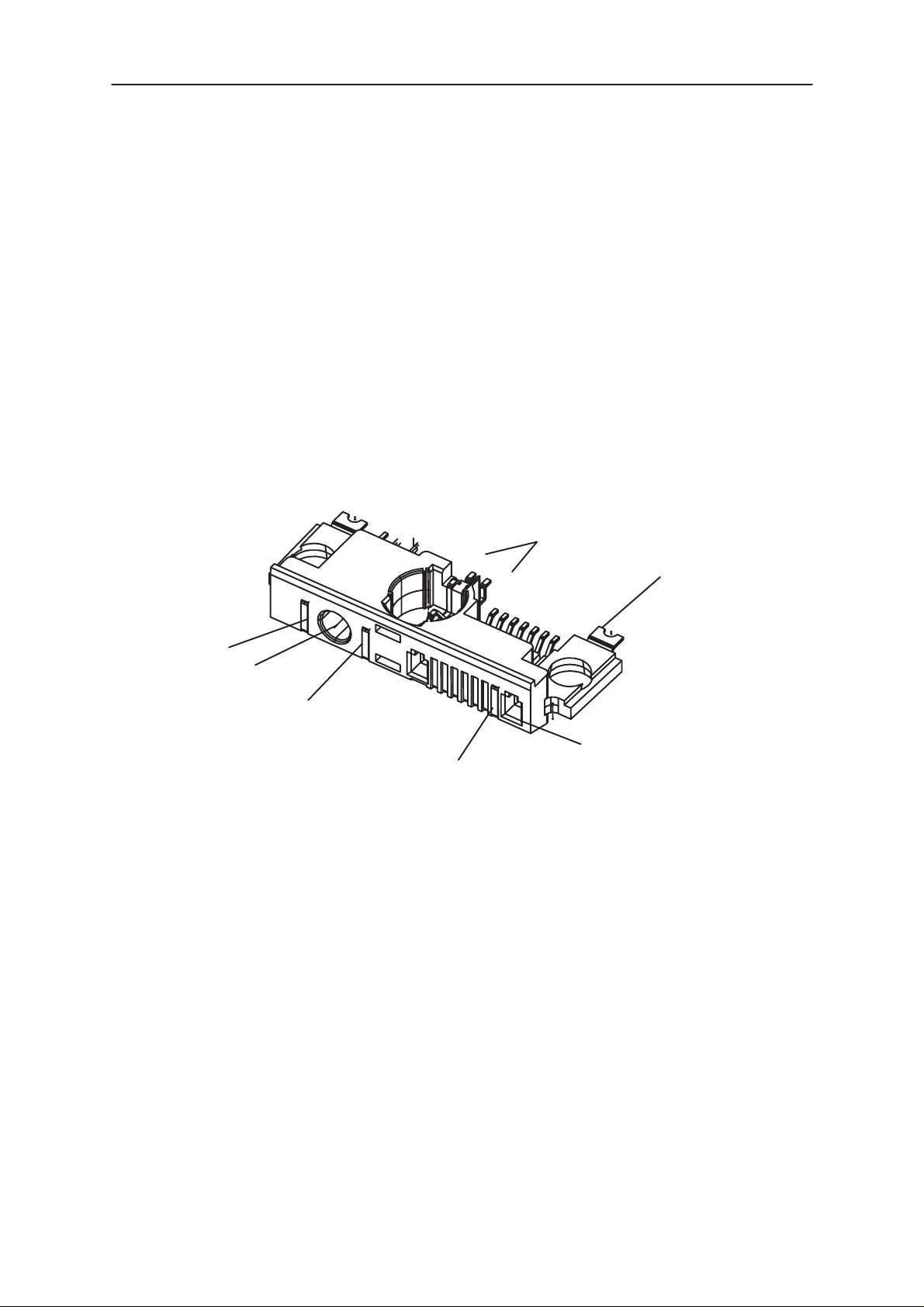
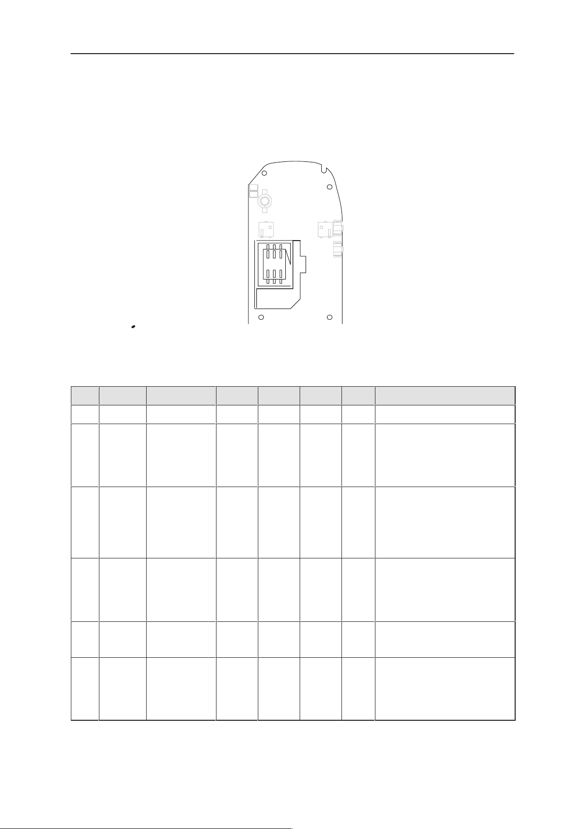
System Connector
This section describes the electrical connection and interface levels
between the baseband, RF and UI parts. The electrical interface
specifications are collected into tables that cover a connector or a defined
interface.
The system connector includes the following parts:
– DC connector for external plug–in charger and a desktop charger
– System connector for accessories and intelligent battery packs
The System connector is used to connect the transceiver to accessories.
System connector pins can also be used to connect intelligent battery
packs to the transceiver.
Contact 1
System Module
2
3
4
6
Slide Detect
7
8
13
Solderable element,
2 pcs
14
DC–jack
2,3,4
Contact 5
Contacts
8...13
Contact 14
Figure 1. System Connector – module
Cable/Cradle connector
guiding/fixing hole, 2 pcs
Amendment 07/00
Page 2– 5
Page 6
NSE–5
System Module
B side view
Fixing pads (2 pcs)
PAMS
Technical Documentation
IBI connector
(6 pads)
14
8
1
7
PCB
DC Jack
Microphone
acoustic ports BB
Bottom
connector (6 pads)
A
B
Charger pads (3 pcs)
A side view
Figure 2. System Connector – detailed.
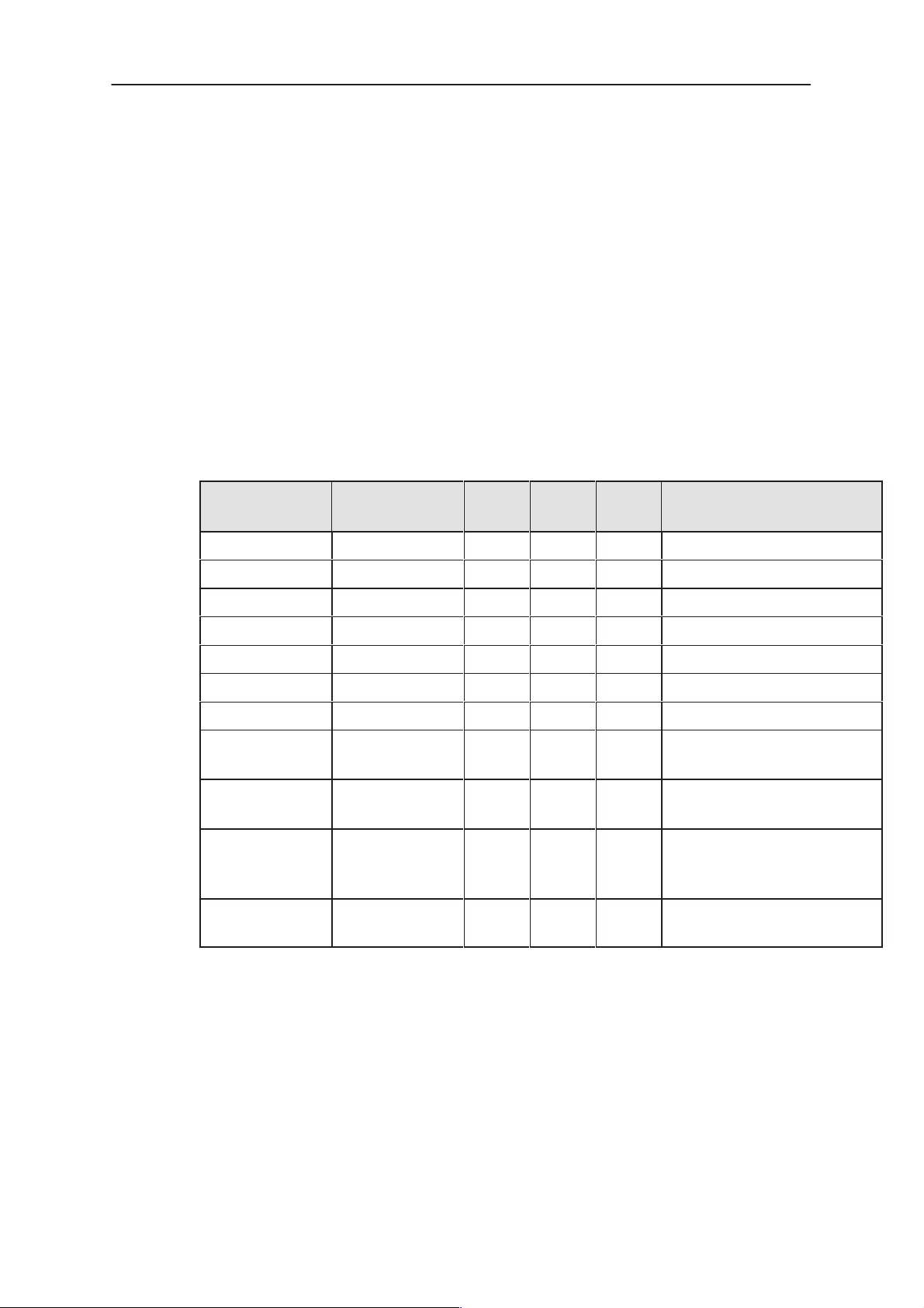
Table 1. System connector signals.
Cable locking holes (3 pcs)
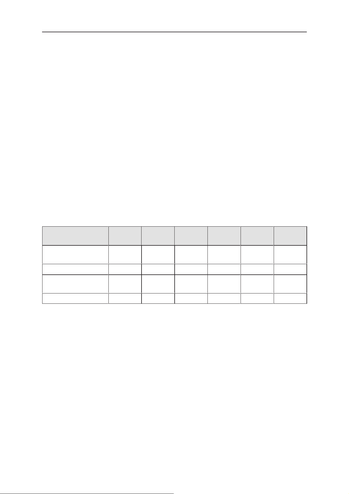
Pin Name Function Description
1 V_IN Bottom charger contacts Charging voltage.
2 L_GND DC Jack Logic and charging ground.
3 V_IN DC Jack Charging voltage.
4 CHRG_CTRL DC Jack Charger control.
5 CHRG_CTRL Bottom charger contacts Charger control.
6 MIC–P Slide Detect Holder Slide Detect
7 MIC–N Slide Detect Holder Gnd
8 XMIC Bottom & IBI connectors Analog audio input, DLR–3
power
9 SGND Bottom & IBI connectors Audio signal ground,
10 XEAR Bottom & IBI connectors Analog audio output.
11 MBUS Bottom & IBI connectors Bidirectional serial bus.
Page 2– 6
Amendment 07/00
Page 7

PAMS
NSE–5
Technical Documentation
Table 1. System connector signals.
(continued)
12 FBUS_RX Bottom & IBI connectors Serial data in.
13 FBUS_TX Bottom & IBI connectors Serial data out.
14 L_GND Bottom charger contacts Logic and charging ground.
System Module
DescriptionFunctionNamePin
DC Connector
The electrical specifications in NO TAG shows the idle voltage produced
by the acceptable chargers at the DC connector input. The absolute
maximum input voltage is 18V due to the transient suppressor that is
protecting the charger input.
Slide Microphone
The microphone is connected to the slide by means of springs it has a
microphone input level specified in NO TAG. The microphone requires
bias current to operate which is generated by the COBBA_GJP ASIC.
Slide Connector
An Interrupt signal to MAD2PR1 determines whether the slide is in an
open or closed position.
Roller Interface
A mechanical solution is implemented and three interrupts are fed to the
MAD2PR1
Keys and Keymatrix
0–9, *, #, send, end, soft_1, soft_2, power_on_off, roller_push,
Headset Connector
The external headset device is connected to the system connector, from
which the signals are routed to COBBA_GJP microphone inputs and
earphone outputs.
Issue 1 07/99
Page 2 – 7
Page 8
NSE–5
aud u
(from
y
accessory
de ec
)
System Module
NA
MICN
mouted
in slide
PAMS
Technical Documentation
Table 2. Mic signals of the system connector
0 2 12.5 mV Connected to COBBA_GJP MIC2N
input. The maximum value corresponds to1 kHz, 0 dBmO network
level with input amplifier gain set to
32 dB. typical value is maximum
value – 16 dB.
NA
MICP
0 2 12.5 mV Connected to COBBA_GJP MIC2P
mounted
in slide
Pin IB-
Name Function Min Typ Max Unit Description
pin
10 Yes XEAR Analog
audio output
phone to
accessor
input. The maximum value corresponds to1 kHz, 0 dBmO network
level with input amplifier gain set to
32 dB. typical value is maximum
value – 16 dB.
Table 3. System/IBI connector
47 W Output AC impedance (ref.
GND) resistor tol. is 5%
10 mF Series output capacitance
16 300 W Load AC impedance to GND:
Headset
4.7 10 kW Load AC impedance to
SGND: External accessory.
Page 2 – 8
Accessory
detection
(fom accessory to
p
phone
1.0 V
Max. output level. No load
p–p
100 kW Resistance to accessory
ground (in accessory)
0.5 V DC Voltage (ref. SGND). External accessory
6.8 kW Load DC resistance to
SGND. External accessory
0 0.2 V DC Voltage (ref. SGND).
Headset with closed switch
16 1500 W Load DC resistance to
SGND. Headset with closed
switch
2.8 V DC Voltage (ref. SGND). No
accessory, or headset with
open switch
47 kW Pull–up resistor to VBB in
phone
Issue 1 07/99
Page 9
PAMS
t
)
to hone)
(
(f
g
(from hone to
NSE–5
Technical Documentation
8 Yes XMIC Analog audio in-
put (from accessory to phone)
Headset microphone inpu
(from accessory
to phone
Accessory mute.
Voltage
p
compared to
SGND.
(from phone to
accessory)
System Module
2.0 2.2 k Input AC impedance
100
1
V
2.0 2.2 k Input AC impedance
2.5 k Headset source AC im-
100 600 A Bias current
200
2.5 2.9 V Not muted
0 1.55 V Muted, without headset
1.6 2.0 2.4 V Comparator reference in
mV-
p–p
Accessory source AC im-
pedance
Maximum signal level
p–
p
pedance
Maximum signal level
accessory
Headset
detection
(from accessory
to phone)
DLR–3 detection
rom accessory to
phone)
9 Yes SGND Audio signal
ground.
Separated from
phone GND
p
accessory)
1.47 2.9 V No headset (ref.
SGND).
0 1.33 V Headset connected
(ref. SGND).
49 k Pull–up resistor to VBB
in phone
1.47 2.9
440 733
49
mV
k
No DLR–3 ((ref SGND)
V
DLR–3 connected (ref.
SGND).
Pull–up resistor to VBB in
phone
47 Output AC impedance
(ref. GND)
10 F Series output capaci-
tance
380 Resistance to phone
ground (DC) (in phone)
Amendment 07/00
100 k Resistance to accesso-
ry ground (in accessory)
–0.2 +0.2 V DC voltage compared
to phone GND
–5 +5 V DC voltage compared
to accessory GND
Page 2– 9
Page 10
NSE–5
to hone)
System Module
PAMS
Technical Documentation
13 Yes FBUS_TXSerial data out
(from phone to
accessory)
12 Yes FBUS_RXSerial data in
(from accessory to phone)
0.1 0.8 V Output low voltage @
I
4 mA (ref. GND)
OL
1.7 2.8 V Output high voltage @
I
4 mA (ref. GND)
OH
47 k Pull–up resistor in
phone
220 k Pull–down resistor in
accessory
47 100 Serial (EMI filtering) re-
sistor in phone
150 pF Cable capacitance
1 s Rise/Fall time
0 0.8 V Input low voltage (ref.
GND)
2.0 2.8 V Input high voltage (ref.
GND)
220 k Pull–down resistor in
phone
47 k Pull–up resistor in ac-
cessory
11 Yes MBUS
FLASH_
CLK
Bidirectional serial bus
Flash serial data
clock
(from accessory
p
2.2 k Serial (EMI filtering) resistor in accessory
150 pF Cable capacitance
2 s Rise/Fall time @
115kbits/s
1 s Rise/Fall time @
230kbits/s
0 0.8 V Input low voltage (ref.
GND)
2.0 2.8 V Input high voltage (ref.
GND)
0 0.8 V
2.1 2.9 V
4.7 k Pull–up resistor in phone
220 k Pull–down resistor in ac-
100 Serial (EMI filtering) resis-
Output low voltage @
I
4 mA (ref. GND)
OL
Output high voltage @
I
100 A (ref. GND)
OH
cessory
tor in phone
Page 2– 10
200 pF Cable capacitance
5
Rise/Fall time @ 9600
s
bits/s
Amendment 07/00
Page 11
PAMS
(f
)
to hone)
NSE–5
Technical Documentation
2,
14
4,5
1,3 –
L_GND Logic and charg-
–
ing ground (separated from
phone GND by
EMI components)
–
CHRG_
CTRL
VIN Fast charger
Charger control
(from phone to
accessory
rom accessory
to phone
Slow charger
(fom accessory
to phone)
System Module
0 1.0 A Ground current
0 0.8 V Output low voltage @ I
20 A
1.7
1 99 % PWM duty cycle
0 8.5 V Charging voltage.
0 0.85 A Charging current.
2.9 V Output high voltage @
I
20 A
OH
32 37 Hz PWM frequency
20 k Serial (EMI filtering) resis-
tor in phone
30 k Pull–down resistor in
phone
100
mV-
p–p
Ripple voltage @ f =
20...200Hz, load = 3 &
10
100
100
200
0
15 V
mV-
p–p
mV-
p–p
mV-
p–p
peak
Ripple voltage @ f =
0.2...30 kHz, load = 3 &
10
Ripple voltage @ f > 30
kHz, load = 3 & 10
Total ripple voltage @ f >
20 Hz, load = 3 & 10
Charging voltage (max. =
unloaded, +20 % overvoltage in mains).
OL
0 1.0
A
Amendment 07/00
Charging current (max. =
pea
shorted, +20 % overvol-
k
tage in mains).
Page 2– 11
Page 12
NSE–5
System Module
PAMS
Technical Documentation
Baseband
HOOKDET
MAD
HEADDET
CCONT
EAD
HF
COBBA
–GJP
AUX
OUT
PD2
GND
10
10k
100n
GND
10u
27p
100n
1u
220k
220k
VBB VBB
2k2 47k
2k2
VBB
47k
47R
100MHz
33R
GND
XEAR
LGND
PC–Board
R01
SW01
+
+
+
C01
C03
C02
HFCM
MIC1N
MIC1P
MIC3N
MIC3P
GND
100n
100n
100n
100n
GND
27p
2k2
27p
2k2
100R
100R
330R
XMIC
SGND
R01= 100R
C01=33uF
L01
C02=1000pF
GND GND GND
C03=22pF
L01=MMZ2012Y6
01BT/TDK
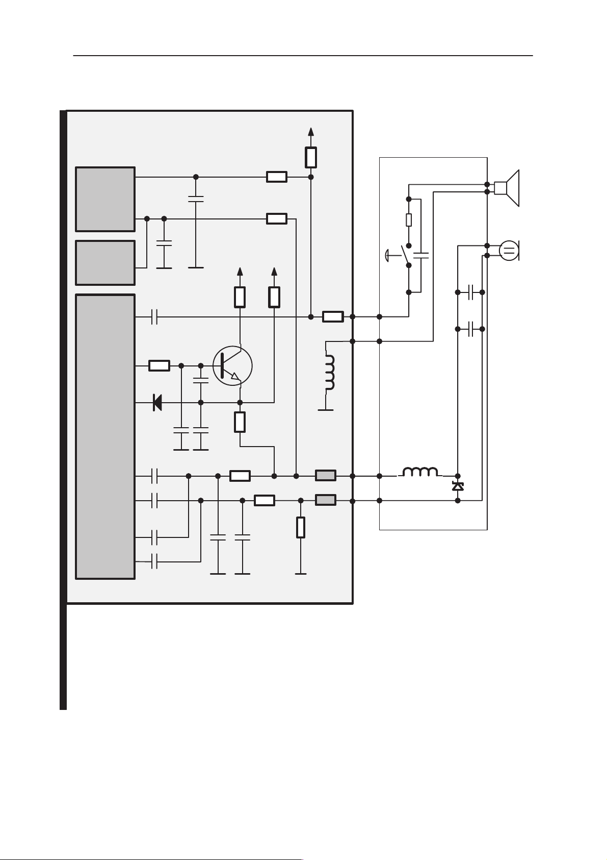
Note 1: Grey resistor are in the border of ”EMI clean” and ”dirty” areas.
Note 2: ESD protection diodes are not shown.
Figure 1. Combined headset, system connector audio signals
Z01
Page 2– 12
Amendment 07/00
Page 13
PAMS
NSE–5
Technical Documentation
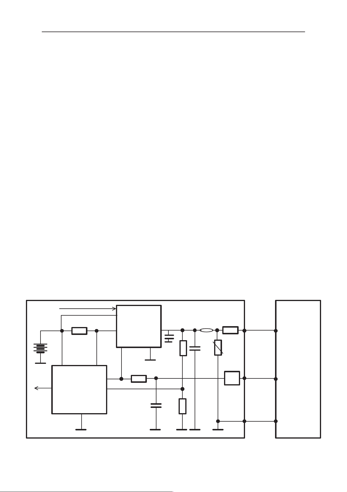
Battery Connector
The BSI contact on the battery connector is used to detect when the
battery is removed with power switched on enabling the SIM card
operation to shut down first. The BSI contact in the battery pack should be
shorter than the supply power contacts to give enough time for the SIM
shut down.
12
34
System Module
No metal in these areas!
old connector type
B side view.
phone
Vibra Alerting Device
A vibra alerting device is used to give a silent signal to the user of an
incoming call it is mounted in the B–cover. A special battery pack contains
a vibra motor. The vibra is controlled with one PWM signal by the
MAD2PR1 via the BTEMP battery terminal.
Figure 4. Battery connector locations
+VBATT
1
BSI
2
BTEMP
3
–VBATT
4
Issue 1 07/99
Page 2 – 13
Page 14
NSE–5
System Module
SIM Card Connector
The SIM card connector is located on the PCB. Only small SIM cards are
supported.
PAMS
Technical Documentation
321
456
Figure 5. Sim Card Reader Ultra phone
Table 4. SIM Connector Electrical Specifications
Pin Name Parameter Min Typ Max Unit Notes
1 GND GND 0 0 V Ground
2 VSIM 5V SIM
Card
4.8
2.8
5.0
3.0
5.2
3.2
V Supply voltage
3V SIM
Card
3 DATA 5V Vin/Vout
3V Vin/Vout
4 SIMRS
T
5V SIM
Card
4.0
0
2.8
0
4.0
2.8
”1”
”0”
”1”
”0”
”1”
”1”
VSIM
0.5
VSIM
0.5
VSIM
VSIM
V SIM data
Trise/Tfall max 1us
V SIM reset
3V SIM
Card
5 SIMCLKFrequency
3.25
MHz
SIM clock
Trise/Tfall
6 VPP 5V SIM
Card
3V SIM
Card
VSIM supply voltages are specified to meet type approval requirements
regardless the tolerances in components.
Page 2 – 14
4.8
2.8
5.0
3.0
25
5.2
3.2
ns
V Programming voltage
pin6 and pin2 tied to-
gether
Issue 1 07/99
Page 15
PAMS
NSE–5
Technical Documentation
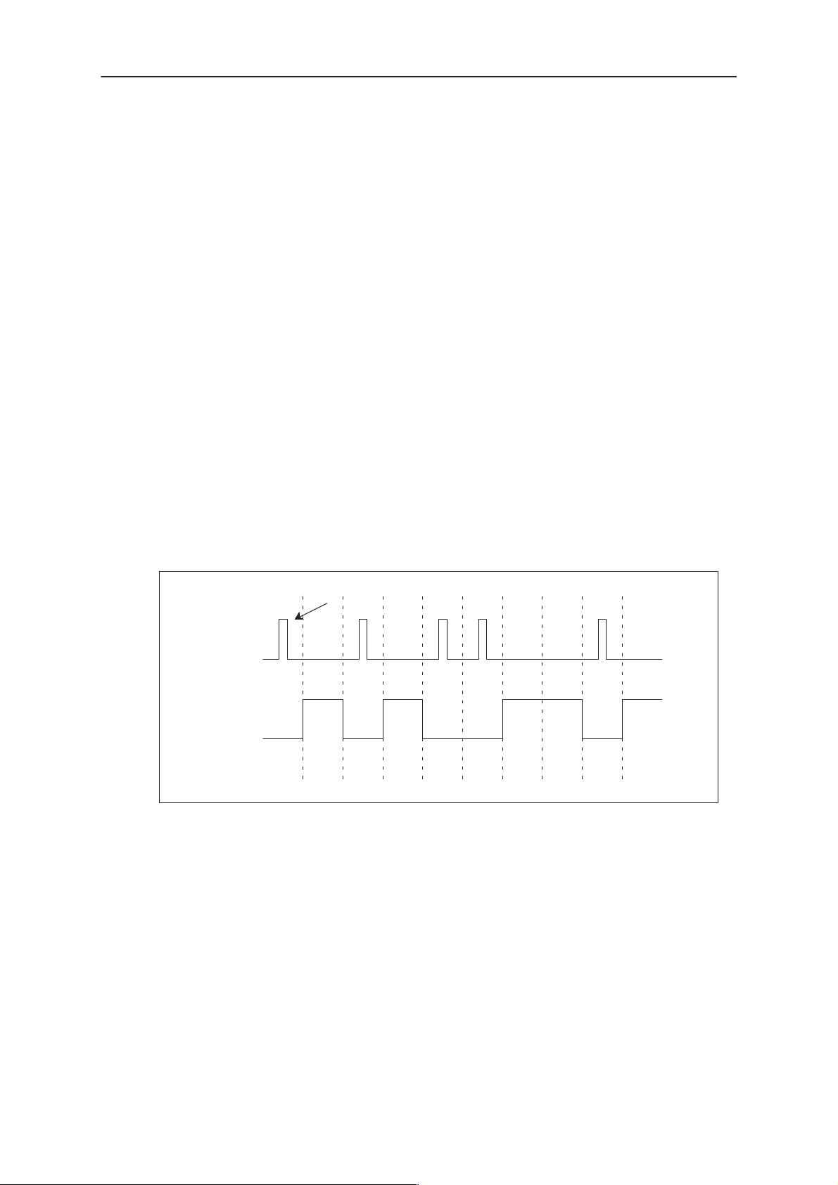
Infrared Transceiver Module
An infrared transceiver module is designed as a substitute for hardwired
connections between the phone and a PC. The infrared transceiver
module is a stand alone component. In DCT3 the module is located
inside and at the top of the phone.
The Rx and Tx is connected to the FBUS via a dual bus buffer. The
module and buffer is activated from the MAD2_pr1 with a pull up on IRON.
The Accif in MAD2_pr1 performs pulse encoding and shaping for
transmitted data pulses and detection and decoding for received data
pulses.
The data is transferred over the IR link using serial FBUS data at speeds
9.6, 19.2, 38.4, 57.6 or 115.2 kbits/s, which leads to maximum throughput
of 92.160 kbits/s. The used IR module complies with the IrDA SIR
specification (Infra Red Data Association), which is based on the HP SIR
(Hewlett–Packard‘s Serial Infra Red) consept.
System Module
The Following figure gives an example of IR transmission pulses. In IR
transmission a light pulse correspondes to 0–bit and a ”dark pulse”
correspondes to 1–bit.
constant pulse
IR TX
UART TX
startbit stopbit1 0100110
Figure 6. IR transmission frame – example
The FBUS cannot be used for external accessory communication, when
the infrared mode is selected. Infrared communication reserves the FBUS
completely.
Issue 1 07/99
Page 2 – 15
Page 16

NSE–5
System Module
Real Time Clock
Requirements for a real time clock implementation are a basic clock
(hours and minutes), a calender and a timer with alarm and power on/off
–function and miscellaneous calls. The RTC will contain only the time
base and the alarm timer but all other functions (e.g. calendar) will be
implemented with the MCU software. The RTC needs a power backup to
keep the clock running when the phone battery is disconnected. The
backup power is supplied from a rechargable polyacene battery that can
keep the clock running for approximately ten minutes. If the backup has
expired, the RTC clock restarts after the main battery is connected. The
CCONT resets the MCU in approx 62ms and the 32kHz source is settled
(after approx. 1s).
The CCONT is an ideal place for an integrated real time clock as the asic
already contains the power up/down functions and a sleep control with the
32kHz sleep clock, which is always running when the phone battery is
connected. This sleep clock is used for a time source to a RTC block.
PAMS
Technical Documentation
Page 2 – 16
Issue 1 07/99
Page 17

PAMS
NSE–5
Technical Documentation
Baseband Module
Technical Summary
The baseband architecture is basically similar to DCT3 GSM phones.
DCT3.5 differs from DCT3 in the single pcb koncept and the seriel
interface between MAD2PR1 and COBBA_GJP and MAD2PR1 and
CCONT. In DCT3.5 the MCU, the system specific ASIC and the DSP are
intergrated into one ASIC, called the MAD2PR1 chip, which takes care of
all the signal processing and operation controlling tasks of the phone.
The baseband architecture supports a power saving function called ”sleep
mode”. This sleep mode shuts off the VCTCXO, which is used as system
clock source for both RF and baseband. During the sleep mode the
system runs from a 32 kHz crystal. The phone is waken up by a timer
running from this 32 kHz clock supply. The sleeping time is determined by
some network parameters. When the sleep mode is entered both the
MCU and the DSP are in standby mode and the normal VCTCXO clock
has been switched off.
System Module
The battery voltage range in DCT3 family is 3.0V to 4.5V depending on
the battery charge and used cell type (Li–Ion or NiMH). Because of the
lower battery voltage the baseband supply voltage is lowered to a nominal
of 2.8V.
The baseband is running from a 2.8V power rail which is supplied by a
power controling asic (CCONT). In the CCONT there are seven
individually controlled regulator outputs for the RF section, one 2.8V
output for the baseband plus a core voltage for MAD2PR1. However this
is not used in NSE–5 because the chipset supports 2.8Volts. In addition
there is one +5V power supply output(V5V). TheCCONTalso contains a
SIM interface which supports both 3V and 5V SIM cards. A real time clock
function is integrated into the CCONT which utilises the same 32KHz
clock supply as the sleep clock. A backup power supply is provided for
the RTC which keeps the real time clock running when the main battery is
removed. The backup power supply is a rechargeable polyacene battery
with a backup time of ten minutes.
The interface between the baseband and the RF section is handled by a
specific asic. The COBBA_GJP asic provides A/D and D/A conversion of
the in–phase and quadrature receive and transmit signal paths and also
A/D and D/A conversions of received and transmitted audio signals to and
from the UI parts. Data transmission between the COBBA_GJP and the
MAD2PR1 is implemented using serial connections. Digital speech
processing is handled by the MAD2PR1 asic. The COBBA_GJP asic is a
dual supply voltage circuit, the digital parts are running from the baseband
supply VBB and the analog parts are running from the analog supply
VCOBBA (VR6).
Issue 1 07/99
Page 2 – 17
Page 18
NSE–5
System Module
PAMS
Technical Documentation
LCD
vibra
motor
IR
roller
TX/RX SIGNALS
COBBA_GJP
AUDIOLINES
BASEBAND
COBBA SUPPLY
MAD2pr1
+
MEMORIES
RF SUPPLIES
CCONT
BB SUPPLY
core voltage
SYSCON
CHAPS
PA SUPPLY
SIM
32kHz
CLK
SLEEP CLOCK
VBAT
13MHz
CLK
SYSTEM CLOCK
BATTERY
NiMH LiIon
Power Distribution
In normal operation the baseband is powered from the phone‘s battery.
The battery consists of one Lithium–Ion cell. There is also a possibility to
use batteries consisting of three Nickel Metal Hydride cells or one Solid
state cell. An external charger can be used for recharging the battery and
supplying power to the phone. The charger can be either so called fast
charger, which can deliver supply current up to 1600 mA or a standard
charger that can deliver approx 300 mA.
The CCONT provides voltage to the circuitry excluding the RF PA, LCD
and IrDa which are supplied via a continuous power rail direct from the
battery. The RF PA module has a cutoff voltage of 3.1V. The battery
note)
feeds power directly to several parts of the system: CCONT, PA and
UI circuitry (display lights, buzzer). The four dedicated control lines,
RxPwr, TxPwr, SIMCardPwr and SynthPwr from MAD2 to CCONT have
changed to a serial control signal between MAD2PR1 and CCONT.
Figure 8 shows a simplified block diagram of the power distribution.
Figure 7. Block Diagram
(see
Note : In battery terms there is VBATT and VB, the difference is a filter (coil and
capacitors)
Page 2 – 18
Issue 1 07/99
Page 19
PAMS
NSE–5
Technical Documentation
The power management circuitry provides protection against
overvoltages, charger failures and pirate chargers etc. that could cause
damage to the phone.
PA SUPPLY
LCD
MODULE
VBB
COBBA_GJP
VBAT
MEMORIES
VCOBBA
MAD2pr1
+
RF SUPPLIES
CCONT
PWRONX
CNTVR
VBB
core voltage
PURX
POWER
MGMT
VSIM
VBAT
PWM
SIM
RTC
BACKUP
sram
BATTERY
System Module
BASEBAND
CONNECTOR
VIN
Figure 8. Baseband power distribution
The heart of the power distrubution is the CCONT. It includes all the
voltage regulators and feeds the power to most of the system. The whole
baseband is powered from the same regulator which provides 2.8V
baseband supply VBB. The baseband regulator is active always when the
phone is powered on. The core baseband regulator feeds, amongst
others, MAD2PR1 and memories, COBBA_GJP digital parts and the LCD
driver in the UI section. COBBA_GJP analog parts are powered from a
dedicated 2.8V supply VCOBBA by the CCONT. There is a separate
regulator for a SIM card which is selectable between 3V and 5V and
controlled by the SIMPwr line from MAD2PR1 to CCONT.
The CCONT contains a real time clock function, which is powered from a
RTC backup when the main battery is disconnected. The RTC backup is
rechargable polyacene battery.
CCONT includes also six additional 2.8V regulators providing power to the
RF section. These regulators can be controlled by the seriel interface from
MAD2PR1 ie RF regulator control register in CCONT which MAD2PR1
can update.
Issue 1 07/99
Page 2 – 19
Page 20
NSE–5
System Module
CCONT supply a core voltage to the MAD2PR1. The core voltage is by
default 1.975V.
RAM backup as in PDC3 phone.
CCONT generates also a 1.5 V reference voltage VREF to COBBA_GJP,
SUMMA. The VREF voltage is also used as a reference to some of the
CCONT A/D converters and as a reference for al the other regulators.
In additon to the above mentioned signals MAD2PR1 includes also TXP
control signal which goes to SUMMA power control block and to the power
amplifier. The transmitter power control TXC is led from COBBA_GJP to
SUMMA.
PAMS
Technical Documentation
Table 5. CCONT current output capability/ nominal voltage
Regulator Maximum
Unit Vout Unit Notes
current
VR1 25 mA 2.8 V VCTCXO
VR2 25 mA 2.8 V CRFU Rx
VR3/switch 50 mA 2.8 V PLL VSYN
VR4 90 mA 2.8 V VCO VSYN
VR5 80 mA 2.8 V PLUSSA Rx
VR6 100 mA 2.8 V COBBA_GJP
VR7 150 mA 2.8 V PLUSSA+CRFU Tx
VBB ON
VBB SLEEP
VSIM 30 mA 3.0/
125
1
mA
mA
2.8
2.8
5.0
V
V
V
V
current limit 250mA
current limit 5mA
VSIM
outout voltage selectable
V_core 50 mA 1.975 V programmable core sup-
ply for cpu/dsp/sys asic
dV=225mV
V_RAM_bck/
VR3
50 mA 2.8 V nomal mode 2.8V. 2.0V
for data retention.
VSIM must fullfill the GSM11.10 current spike requirements.
VSIM and V5V can give a total of 30 mA.
Page 2 – 20
Issue 1 07/99
Page 21

PAMS
NSE–5
Technical Documentation
Power Up
The baseband is powered up by:
1. Pressing the power key, that generates a PWRONX interrupt
signal from the power key to the CCONT, which starts the power up procedure.
2. Connecting a charger to the phone. The CCONT recognizes
the charger from the VCHAR voltage and starts the power up
procedure.
3. A RTC interrupt. If the real time clock is set to alarm and the
phone is switched off, the RTC generates an interrupt signal,
when the alarm is gone off. The RTC interrupt signal is connected to the PWRONX line to give a power on signal to the
CCONT just like the power key.
System Module
4. A battery interrupt. Intelligent battery packs have a possibility
to power up the phone. When the battery gives a short (10ms)
voltage pulse through the BTEMP pin, the CCONT wakes up
and starts the power on procedure.
Power up with a charger
When the charger is connected CCONT will switch on the CCONT digital
voltage as soon as the battery voltage exeeds 3.0V. The reset for
CCONT’s digital parts is released when the operating voltage is stabilized
( 50 us from switching on the voltages). Operating voltage for VCXO is
also switched on. The counter in CCONT digital section will keep MAD in
reset for 62 ms (PURX) to make sure that the clock provided by VCXO is
stable. After this delay MAD reset is relased, and VCXO –control
(SLEEPX) is given to MAD. The diagram assumes empty battery, but the
situation would be the same with full battery:
When the phone is powered up with an empty battery pack using the
standard charger, the charger may not supply enough current for standard
powerup procedure and the powerup must be delayed.
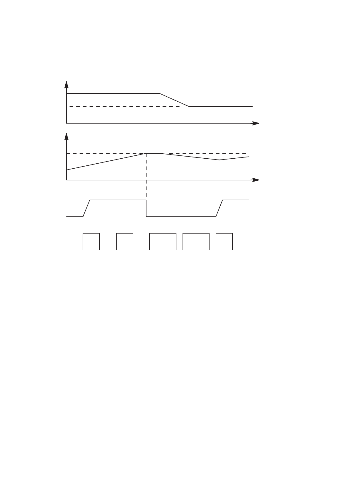
Power Up With The Power Switch (PWRONX)
When the power on switch is pressed the PWRONX signal will go low.
CCONT will switch on the CCONT digital section and VCXO as was the
case with the charger driven power up. If PWRONX is low when the 64 ms
delay expires, PURX is released and SLEEPX control goes to MAD. If
PWRONX is not low when 64 ms expires, PURX will not be released, and
CCONT will go to power off ( digital section will send power off signal to
analog parts)
Issue 1 07/99
Page 2 – 21
Page 22
NSE–5
System Module
PAMS
Technical Documentation
SLEEPX
PURX
CCPURX
PWRONX
VR1,VR6
VBB (2.8V)
Vchar
12 3
1:Power switch pressed ==> Digital voltages on in CCONT (VBB)
2: CCONT digital reset released. VCXO turned on
3: 62 ms delay to see if power switch is still pressed.
Power Up by RTC
RTC ( internal in CCONT) can power the phone up by changing RTCPwr
to logical ”1”. RTCPwr is an internal signal from the CCONT digital
section.
Power Up by IBI
IBI can power CCONT up by sending a short pulse to logical ”1”. RTCPwr
is an internal signal from the CCONT digital section.
Acting Dead
If the phone is off when the charger is connected, the phone is powered
on but enters a state called ”acting dead”. To the user the phone acts as if
it was switched off. A battery charging alert is given and/or a battery
charging indication on the display is shown to acknowledge the user that
the battery is being charged.
Active Mode
In the active mode the phone is in normal operation, scanning for
channels, listening to a base station, transmitting and processing
information. All the CCONT regulators are operating. There are several
substates in the active mode depending on if the phone is in burst
reception, burst transmission, if DSP is working etc..
Page 2 – 22
Issue 1 07/99
Page 23
PAMS
NSE–5
Technical Documentation
Sleep Mode
In the sleep mode all the regulators except the baseband VBB, Vcore and
the SIM card VSIM regulators are off. Sleep mode is activated by the
MAD2PR1 after MCU and DSP clocks have been switched off. The
voltage regulators for the RF section are switched off and the VCXO
power control, VCXOPwr is set low. In this state only the 32 kHz sleep
clock oscillator in CCONT is running. The flash memory power down input
is connected to the VCXO power control, so that the flash is deep
powered down during sleep mode.
The sleep mode is exited either by the expiration of a sleep clock counter
in the MAD2PR1 or by some external interrupt, generated by a charger
connection, key press, headset connection etc. The MAD2PR1 starts the
wake up sequence and sets the VCXOPwr control high. After VCXO
settling time other regulators and clocks are enabled for active mode.
If the battery pack is disconnect during the sleep mode, the CCONT shall
power down the SIM in the sleep mode as there is no time to wake up the
MCU.
System Module
Battery charging
MAD
VBAT
MAD
CCONTINT
CCONT
The electrical specifications give the idle voltages produced by the
acceptable chargers at the DC connector input. The absolute maximum
input voltage is 30V due to the transient suppressor that is protecting the
charger input. At phone end there is no difference between a plug–in
charger or a desktop charger. The DC–jack pins and bottom connector
charging pads are connected together inside the phone.
0R22
PWM_OUT
ICHAR
VCHAR
LIM
VOUT
CHAPS
RSENSE
PWM
VCH
GND
22k
1n
TRANSCEIVER
27pf
47k
33R/100MHz
1u
30V
1.5A
EMI
VIN
CHRG_CTRL
CHARGER
NOT IN
ACP–7/8
GND
Issue 1 07/99
47k
Figure 9. Battery Charging
L_GND
Page 2 – 23
Page 24
NSE–5
System Module
Startup Charging
When a charger is connected, the CHAPS is supplying a startup current
minimum of 130mA to the phone. The startup current provides initial
charging to a phone with an empty battery. Startup circuit charges the
battery until the battery voltage level is reaches 3.0V (+/– 0.1V) and the
CCONT releases the PURX reset signal and program execution starts.
Charging mode is changed from startup charging to PWM charging that is
controlled by the MCU software. If the battery voltage reaches 3.55V
(3.75V maximum) before the program has taken control over the charging,
the startup current is switched off. The startup current is switched on
again when the battery voltage is sunken 100mV (nominal).
Parameter Symbol Min Typ Max Unit
PAMS
Technical Documentation
Table 6.
VOUT Start– up mode cutoff limit Vstart 3.45 3.55 3.75 V
VOUT Start– up mode hysteresis
NOTE: Cout = 4.7 uF
Start–up regulator output current
VOUT = 0V ... Vstart
Vstarthys 80 100 200 mV
Istart 130 165 200 mA
Battery Overvoltage Protection
Output overvoltage protection is used to protect phone from damage. This
function is also used to define the protection cutoff voltage for different
battery types (Li or Ni). The power switch is immediately turned OFF if the
voltage in VOUT rises above the selected limit VLIM1 or VLIM2.
Table 7.
Parameter Symbol LIM input Min Typ Max Unit
Output voltage cutoff limit
(during transmission or Li–
battery)
Output voltage cutoff limit
(no transmission or Ni–bat-
tery)
VLIM1 LOW 4.4 4.6 4.8 V
VLIM2 HIGH 4.8 5.0 5.2 V
The voltage limit (VLIM1 or VLIM2) is selected by logic LOW or logic HIGH
on the CHAPS (N101) LIM– input pin. Default value is lower limit VLIM1.
When the switch in output overvoltage situation has once turned OFF, it
stays OFF until the the battery voltage falls below VLIM1 (or VLIM2) and
PWM = LOW is detected. The switch can be turned on again by setting
PWM = HIGH.
Page 2 – 24
Issue 1 07/99
Page 25
PAMS
NSE–5
Technical Documentation
VCH
VCH<VOUT
VOUT
VLIM1 or VLIM2
System Module
t
t
SWITCH
PWM (32Hz)
ON OFF
Battery Removal During Charging
Output overvoltage protection is also needed in case the main battery is
removed when charger connected or charger is connected before the
battery is connected to the phone.
With a charger connected, if VOUT exceeds VLIM1 (or VLIM2), CHAPS
turns switch OFF until the charger input has sunken below Vpor (nominal
3.0V, maximum 3.4V). MCU software will stop the charging (turn off PWM)
when it detects that battery has been removed. The CHAPS remains in
protection state as long as PWM stays HIGH after the output overvoltage
situation has occured.
ON
Issue 1 07/99
Page 2 – 25
Page 26
NSE–5
System Module
PAMS
Technical Documentation
VCH
(Standard
Charger)
VOUT
PWM
SWITCH
Vpor
VLIM
4V
Vstart
”1”
”0”
ON
OFF
Droop depends on load
& C in phone
2
4
5
6
7
Istart off due to VCH<Vpor
Vstarthys
t
t
t
1.1Battery removed, (standard) charger connected, VOUT rises (follows charger voltage)
2. VOUT exceeds limit VLIM(X), switch is turned immediately OFF
3.3VOUT falls (because no battery) , also VCH<Vpor (standard chargers full–rectified
output). When VCH > Vpor and VOUT < VLIM(X) –> switch turned on again (also PWM
is still HIGH) and VOUT again exceeds VLIM(X).
4. Software sets PWM = LOW –> CHAPS does not enter PWM mode
5. PWM low –> Startup mode, startup current flows until Vstart limit reached
6. VOUT exceeds limit Vstart, Istart is turned off
7. VCH falls below Vpor
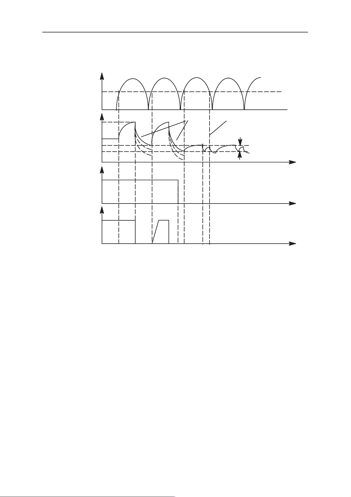
Different PWM Frequencies ( 1Hz and 32 Hz)
When a travel charger (2– wire charger) is used, the power switch is
turned ON and OFF by the PWM input when the PWM rate is 1Hz. When
PWM is HIGH, the switch is ON and the output current Iout = charger
current – CHAPS supply current. When PWM is LOW, the switch is OFF
and the output current Iout = 0. To prevent the switching transients
inducing noise in audio circuitry of the phone soft switching is used.
The performance travel charger (3– wire charger) is controlled with PWM
at a frequency of 32Hz. When the PWM rate is 32Hz CHAPS keeps the
power switch continuously in the ON state.
Page 2 – 26
Issue 1 07/99
Page 27
PAMS
NSE–5
Technical Documentation
SWITCH
PWM (1Hz)
SWITCH
PWM (32Hz)
System Module
ON ONON OFF OFF
ON
Battery Identification
Different battery types are identified by a pulldown resistor inside the
battery pack. The BSI line inside transceiver has a 100k pullup to VBB.
The MCU can identify the battery by reading the BSI line DC–voltage level
with a CCONT (N100) A/D–converter.
BATTERY
R
BVOLT
Vibra Schematic
BTEMP
BSI
s
BGND
Vbb
100k
10k
10n
TRANSCEIVER
BSI
SIMCardDetX
CCONT
MAD
Issue 1 07/99
Figure 10. Battery Identification
Page 2 – 27
Page 28
NSE–5
System Module
The battery identification line is used also for battery removal detection.
The BSI line is connected to a SIMCardDetX line of MAD2 (D200).
SIMCardDetX is a threshold detector with a nominal input switching level
0.85xVcc for a rising edge and 0.55xVcc for a falling edge. The battery
removal detection is used as a trigger to power down the SIM card before
the power is lost. The BSI contact in the battery pack is made 0.7mm
shorter than the supply voltage contacts so that there is a delay between
battery removal detection and supply power off,
0.850.05 Vcc
0.550.05 Vcc
GND
PAMS
Technical Documentation
Vcc
SIMCARDDETX
SIGOUT
Battery Temperature
The battery temperature is measured with a NTC inside the battery pack.
The BTEMP line inside transceiver has a 100k pullup to VREF. The MCU
can calculate the battery temperature by reading the BTEMP line
DC–voltage level with a CCONT (N100) A/D–converter.
BATTERY
R
T
NTC
BVOLT
BSI
BTEMP
BGND
1k
TRANSCEIVER
VREF
Vibra Schematic
100k
10k
2k2
10n
BTEMP
VibraPWM
CCONT
MAD
Page 2 – 28
MCUGenIO4
Figure 11. Battery Temperature
Issue 1 07/99
Page 29
PAMS
NSE–5
Technical Documentation
Supply Voltage Regulators
The heart of the power distrubution is the CCONT. It includes all the
voltage regulators and feeds the power to the whole system. The
baseband digital parts are powered from the VBB regulator which
provides 2.8V baseband supply. The baseband regulator is active always
when the phone is powered on. The VBB baseband regulator feeds MAD
and memories, COBBA digital parts and the LCD driver in the UI section.
There is a separate regulator for a SIM card. The regulator is selectable
between 3V and 5V and controlled by the SIMPwr line from MAD to
CCONT. The COBBA analog parts are powered from a dedicated 2.8V
supply VCOBBA. The CCONT supplies also 5V for RF and for flash VPP.
The CCONT contains a real time clock function, which is powered from a
RTC backup when the main battery is disconnected.
The RTC backup is rechargable polyacene battery, which has a capacity
of 50uAh (@3V/2V) The battery is charged from the main battery voltage
by the CHAPS when the main battery voltage is over 3.2V. The charging
current is 200uA (nominal).
System Module
Table 8.
Operating mode Vref RF REG VCOB-
VBB VSIM SIMIF
BA
Power off Off Off Off Off Off Pull
down
Power on On On/Off On On On On/Off
Reset On Off
VR1 On
On On Off Pull
down
Sleep On Off On On On On/Off
Note: CCONT includes also five additional 2.8V regulators providing power to the RF
section. These regulators can be controlled either by the direct control signals from MAD
or by the RF regulator control register in CCONT which MAD can update. Below are the
listed the MAD control lines and the regulators they are controlling.
–
TxPwr controls VTX regulator (VR5)
–
RxPwr controls VRX regulator (VR2)
–
SynthPwr controls VSYN_1 and VSYN_2 regulators (VR4 and VR3)
–
VCXOPwr controls VXO regulator (VR1)
CCONT generates also a 1.5 V reference voltage VREF to COBBA,
PLUSSA and CRFU. The VREF voltage is also used as a reference to
some of the CCONT A/D converters.
In additon to the above mentioned signals MAD includes also TXP control
signal which goes to PLUSSA power control block and to the power
amplifier. The transmitter power control TXC is led from COBBA to
PLUSSA.
Issue 1 07/99
Page 2 – 29
Page 30

NSE–5
System Module
Audio Control
The audio control and processing is taken care by the COBBA–GJP,
which contains the audio and RF codecs, and the MAD2, which contains
the MCU, ASIC and DSP blocks handling and processing the audio
signals.
Slide
PAMS
Technical Documentation
EMI
System
Connector
Display
XMIC
SGND
XEAR
EMI
Bias +
EMI+ACC
Interf.
EMI
HFCM
AuxOut
Preamp
MIC2
MIC1
MIC3
HF
EAR
COBBA
Multipl.Premult.
Amp Multipl.
Figure 12. Audio Control
Pre
& LP
LP
MAD
DSP
MCU
A
D
Buzzer
Driver
Circuit
D
A
Buzzer
The baseband supports three microphone inputs and two earphone
outputs. The inputs can be taken from an internal microphone, a headset
microphone or from an external microphone signal source. The
microphone signals from different sources are connected to separate
inputs at the COBBA–GJP asic. Inputs for the microphone signals are
differential type.
The MIC1 inputs are used for a headset microphone that can be
connected directly to the system connector. The internal microphone is
connected to MIC2 inputs and an external pre–amplified microphone
(handset/handfree) signal is connected to the MIC3 inputs. In COBBA
there are also three audio signal outputs of which dual ended EAR lines
are used for internal earpiece and HF line for accessory audio output. The
third audio output AUXOUT is used only for bias supply to the headset
microphone. As a difference to DCT2 generation the SGND ( = HFCM at
COBBA) does not supply audio signal (only common mode). Therefore
there are no electrical loopback echo from downlink to uplink.
Page 2 – 30
Issue 1 07/99
Page 31

PAMS
NSE–5
Technical Documentation
The output for the internal earphone is a dual ended type output capable
of driving a dynamic type speaker. The output for the external accessory
and the headset is single ended with a dedicated signal ground SGND.
Input and output signal source selection and gain control is performed
inside the COBBA–GJP asic according to control messages from the
MAD2. Keypad tones, DTMF, and other audio tones are generated and
encoded by the MAD2 and transmitted to the COBBA–GJP for decoding.
Internal Microphone and Earpiece
The baseband supports three microphone inputs and two earphone
outputs. The inputs can be taken from an internal microphone, a headset
microphone or from an external microphone signal source. The
microphone signals from different sources are connected to separate
inputs to the COBBA_GJP asic. Inputs for the microphone signals are of a
differential type.
External Audio Connections
System Module
The external audio connections are presented in figure 16. A headset can
be connected directly to the system connector. The headset microphone
bias is supplied from COBBA AUXOUT output and fed to microphone
through XMIC line. The 330ohm resistor from SGND line to
AGNDprovides a return path for the bias current.
Issue 1 07/99
Page 2 – 31
Page 32

NSE–5
System Module
PAMS
Technical Documentation
Baseband
HOOKDET
MAD
HEADDET
EADCCONT
H
F
COBBA–
GJP
AUXOUT
10
10k
AGND
100n
AGND
27p
100n
220k
220k
VBB VBB
2k2 47k
VBB
47k
33R
100MHz
47R
XEAR
LGN
D
PC–Board
R01
SW01
+
+
+
C01
C03
C02
PD2
HFC
M
MIC1
N
MIC1
P
MIC3
N
MIC3
P
330R
AGND
100R
100R
XMI
C
SGN
D
R01= 100R
C01=33uF
C02=1000pF
C03=22pF
L01=MMZ2012Y6
01BT/TDK
1u
10u
AGND
AGND
100n
100n
100n
100n
Note 1: Grey resistor are in the border of ”EMI clean” and ”dirty” areas.
Note 2: AGND is connected directly to the GND on PCB close to HF parts.
Note 3: ESD protection diodes are not shown.
27p
AGND AGND AGND
2k2
2k2
2k2
27p
Figure 13. Combined headset and system connector audio signal
L01
Z01
Page 2 – 32
Issue 1 07/99
Page 33

PAMS
NSE–5
Technical Documentation
System Module
Analog Audio Accessory Detection
In XEAR signal there is a 47 k pullup in the transceiver and 6.8 k
pull–down to SGND in accessory. The XEAR is pulled down when an
accessory is connected, and pulled up when disconnected. The XEAR is
connected to the HookDet line (in MAD), an interrupt is given due to both
connection and disconnection. There is filtering between XEAR and
HookDet to prevent audio signal giving unwanted interrupts.
External accessory notices powered–up phone by detecting voltage in
XMIC line. In Table 9 there is a truth table for detection signals.
Table 9.
Accessory connected HookDet HeadDet Notes
No accessory connected High High Pullups in the transceiver
Headset HDC–9 with a button switch
pressed
Headset HDC–9 with a button switch re-
leased
Low Low XEAR and XMIC loaded (dc)
High Low *) XEAR unloaded (dc)
Handsfree (HFU–1) Low High XEAR loaded (dc)
Internal Audio Connections
The speech coding functions are performed by the DSP in the MAD2 and
the coded speech blocks are transferred to the COBBA–GJP for digital to
analog conversion, down link direction. In the up link direction the PCM
coded speech blocks are read from the COBBA–GJP by the DSP.
There are two separate interfaces between MAD2 and COBBA–GJP: a
parallel bus and a serial bus. The parallel bus has 12 data bits, 4 address
bits, read and write strobes and a data available strobe. The parallel
interface is used to transfer all the COBBA–GJP control information (both
the RFI part and the audio part) and the transmit and receive samples.
The serial interface between MAD2 and COBBA–GJP includes transmit
and receive data, clock and frame synchronisation signals. It is used to
transfer the PCM samples. The frame synchronisation frequency is 8 kHz
which indicates the rate of the PCM samples and the clock frequency is 1
MHz. COBBA is generating both clocks.
4–wire PCM Serial Interface
The interface consists of following signals: a PCM codec master clock
(PCMDClk), a frame synchronization signal to DSP (PCMSClk), a codec
transmit data line (PCMTX) and a codec receive data line (PCMRX). The
COBBA–GJP generates the PCMDClk clock, which is supplied to DSP
SIO. The COBBA–GJP also generates the PCMSClk signal to DSP by
dividing the PCMDClk. The PCMDClk frequency is 1.000 MHz and is
generated by dividing the RFIClk 13 MHz by 13. The COBBA–GJP further
divides the PCMDClk by 125 to get a PCMSClk signal, 8.0 kHz.
Issue 1 07/99
Page 2 – 33
Page 34

NSE–5
System Module
PCMDClk
PCMSClk
PAMS
Technical Documentation
PCMTxData
PCMRxData
The output for the internal earphone is a dual ended type output capable
of driving a dynamic type speaker. The output for the external accessory
and the headset is single ended with a dedicated signal ground SGND.
Input and output signal source selection and gain control is performed
inside the COBBA_GJP asic according to control messages from the
MAD2PR1. Keypad tones, DTMF, and other audio tones are generated
and encoded by the MAD2PR1 and transmitted to the COBBA_GJP for
decoding. MAD2PR1 generates two separate PWM outputs, one for a
buzzer and one for vibra (internal and external via BTEMP).
Speech Processing
The speech coding functions are performed by the DSP in the MAD2PR1
and the coded speech blocks are transferred to the COBBA_GJP for
digital to analog conversion, down link direction. In the up link direction the
PCM coded speech blocks are read from the COBBA_GJP by the DSP.
sign extended
15 14 13 12 011 10
sign extended
MSB
MSB
LSB
LSB
There are two options for the PCM interface between MAD2PR1 and
COBBA_GJP. The 4 pin solution and a one pin solution. The four pin serial
interface between MAD2PR1 and COBBA_GJP includes transmit and
receive data, clock and frame synchronisation signals. It is used to
transfer the PCM samples. The frame synchronisation frequency is 8 kHz
which indicates the rate of the PCM samples and the clock frequency is 1
MHz. COBBA_GJP generates both clocks. NSE–5 uses the 4–pin
solution.
Alert Signal Generation
A buzzer is used for giving alerting tones and/or melodies as a signal of
an incoming call. Also keypress and user function response beeps are
generated with the buzzer. The buzzer is controlled with a BuzzerPWM
output signal from the MAD2PR1. A dynamic type of buzzer is used since
the supply voltage available can not produce the required sound pressure
for a piezo type buzzer. The low impedance buzzer is connected to an
output transistor that gets drive current from the PWM output. The alert
volume can be adjusted either by changing the pulse width causing the
level to change or by changing the frequency to utilize the resonance
frequency range of the buzzer.
Page 2 – 34
Issue 1 07/99
Page 35

PAMS
NSE–5
Technical Documentation
A vibra alerting device is used for giving a silent signal to the user of an
incoming call. The device is controlled with a VibraPWM output signal
from the MAD2PR1. The vibra alert can be adjusted either by changing
the pulse width or by changing the pulse frequency. The vibra device is
inside the phone, but a special vibra battery can also be used.
Digital Control
MAD2PR1
The baseband functions are controlled by the MAD2PR1 asic, which
consists of a MCU, a system ASIC and a DSP. The GSM/PCN specific
asic is named as MAD2. There are separate controller asics in TDMA and
JDC named as MAD1 and MAD3. All the MAD2PR1 asics contain the
same core processors and similar building blocks, but differ from each
other in system specific functions, pinout and package types.
MAD2PR1 contains following building blocks:
– ARM RISC processor with both 16–bit instruction set (THUMB mode)
and 32–bit instruction set (ARM mode)
System Module
– TMS320C542 DSP core with peripherials:
– API (Arm Port Interface memory) for MCU–DSP commu-
nication, DSP code download, MCU interrupt handling vec-
tors (in DSP RAM) and DSP booting
– Serial port (connection to PCM)
– Timer
– DSP memory
– BUSC (BusController for controlling accesses from ARM to API, Sys-
tem Logic and MCU external memories, both 8– and 16–bit memories)
– System Logic
– CTSI (Clock, Timing, Sleep and Interrupt control)
– MCUIF (Interface to ARM via BUSC). Contains MCU Boo-
tROM
– DSPIF (Interface to DSP)
– MFI (Interface to COBBA_GJP AD/DA Converters)
– CODER (Block encoding/decoding and A51&A52 ciphering)
– AccIF(Accessory Interface)
– SCU (Synthesizer Control Unit for controlling 2 separate
synthesizer)
– UIF (Keyboard interface, serial control interface for COB-
BA_GJP PCM Codec, LCD Driver and CCONT)
– UIF+ (roller/ slide handling)
– SIMI (SimCard interface with enhanched features)
– PUP (Parallel IO, USART and PWM control unit for vibra
and buzzer)
Issue 1 07/99
Page 2 – 35
Page 36

NSE–5
System Module
The MAD2PR1 operates from a 13 MHz system clock, which is generated
from the 13Mhz VCXO frequency. The MAD2PR1 supplies a 6,5MHz or a
13MHz internal clock for the MCU and system logic blocks and a 13MHz
clock for the DSP, where it is multiplied to TBD MHz DSP clock. The
system clock can be stopped for a system sleep mode by disabling the
VCXO supply power from the CCONT regulator output. The CCONT
provides a 32kHz sleep clock for internal use and to the MAD2PR1, which
is used for the sleep mode timing. The sleep clock is active when there is
a battery voltage available i.e. always when the battery is connected.
MAD2PR1 pinout
MAD2PR1 pins and their usage are described in the following table.
PAMS
Technical Documentation
– FLEXPOOL (DAS00308 FlexPool Specification)
– SERRFI (DAS00348 COBBA_GJP Specifications)
Table 10. MAD2PR1 pin list
Pad
No
1 MCUGenIO0 IO 2 BattIO x205 ee-
2fp Col0 IO 2 down keypad matrix key
3 LEADGND0 PWR digital gnd gnd
4 Col1 IO 2 keypad matrix key
5 Col2 IO 2 keypad matrix key
6 Col3 IO 2 keypad matrix key
7 Col4 IO 2 no connection Vol up
8 LCDCSX IO 2 seriel LCD chip select
9 GND0 PWR digital gnd gnd
10 Row5LCDCD IO 2 up Seriel LCD command/data
11 Row4 IO 2 up keypad matrix
12 LEADVCC0 PWR V_core
13 Row3 IO 2 up keypad matrix
Pad Name Direction Drive +
pull
Explanation macro
functions
prom ser-
iel data
sda
and row5
14 Row2 IO 2 up keypad matrix
15 Row1 IO 2 up keypad matrix
16fp Row0 IO 2 up keypad matrix (+powerkey)
17fp (JTDO) IO 2 up flex pool JTDO de-
18 VCCSYS0 PWR V_core
19fp (JTRst) IO 2 down flex pool JTRst
20fp (JTClk) IO 2 up flex pool JTClk
21 VCCIO0 PWR Vbb
Page 2 – 36
fault on
Issue 1 07/99
Page 37

PAMS
NSE–5
Technical Documentation
No
22fp (JTDI) IO 2 up flex pool JTDi
23fp (JTMS) IO 2 up flex pool JTMS
24 LEADGND1 PWR digital gnd
25fp (CoEmu0) IO 2 up flex pool CoEmu0
26fp (CoEmu1) IO 2 up flex pool CoEmu1
27 GND1 PWR digital gnd
28 MCUAd0 O 2 lsb sram+flash adresse 0 mcu ad0
29 MCUAd1 O 2 sram+flash adresse 1 mcu ad1
30 MCUAd2 O 2 sram+flash adresse 2 mcu ad2
31 MCUAd3 O 2 sram+flash adresse 3 mcu ad3
Table 10. MAD2PR1 pin list
DirectionPad NamePad
pull
System Module
ExplanationDrive +
macro
functions
DSP,MCU
DSP,MCU
32 ARMGND PWR digital gnd gnd
33 MCUAd4 O 2 sram+flash adresse 4 mcu ad4
34 MCUAd5 O 2 sram+flash adresse 5 mcu ad5
35 MCUAd6 O 2 sram+flash adresse 6 mcu ad6
36 MCUAd7 O 2 sram+flash adresse 7 mcu ad7
37 MCUAd8 O 2 sram+flash adresse 8 mcu ad8
38 MCUAd9 O 2 sram+flash adresse 9 mcu ad9
39 MCUAd10 O 2 sram+flash adresse 10 mcu ad10
40 MCUAd11 O 2 sram+flash adresse 11 mcu ad11
41 ARMVCC PWR V_core
42 MCUAd12 O 2 sram+flash adresse 12 mcu ad12
43 MCUAd13 O 2 sram+flash adresse 13 mcu ad13
44 VCCSYS1 PWR V_core
45 MCUAd14 O 2 sram+flash adresse 14 mcu ad14
46 GND2 PWR digital gnd
47 MCUAd15 O 2 sram+flash adresse 15 mcu ad15
48 MCUAd16 O 2 msb sram+flash adresse 16 mcu ad16
49 MCUAd17 O 2 flash adresse 17 mcu ad17
50 MCUAd18 O 2 flash adresse 18 mcu ad18
51 MCUAd19 O 2 flash adresse 19 mcu ad19
52fp MCUAd20 IO 2 down reserved for 32Mbit flash 20 /
roller ?
53fp (MCUAd21) IO 2 down roller nWait
54 MCURdX O 2 read strobe
55 MCUWrX O 2 write strobe
Issue 1 07/99
mcu ad20
Page 2 – 37
Page 38

NSE–5
System Module
PAMS
Technical Documentation
Table 10. MAD2PR1 pin list
DirectionPad NamePad
No
56 VCCIO1 PWR Vbb
57 ExtMCUDa0 IO 2 down lsb sram+flash data 0
58 ExtMCUDa1 IO 2 down sram+flash data 1
59 ExtMCUDa2 IO 2 down sram+flash data 2
60 ExtMCUDa3 IO 2 down sram+flash data 3
61 ExtMCUDa4 IO 2 down sram+flash data 4
62 ExtMCUDa5 IO 2 down sram+flash data 5
63 ExtMCUDa6 IO 2 down sram+flash data 6
64 GND3 PWR digital gnd
65 ExtMCUDa7 IO 2 down msb sram+flash data 7
66 VCCSYS2 PWR V_core
67 MCUGenIODa0 IO 2 down flash data 8
68 MCUGenIODa1 IO 2 down flash data 9
69 MCUGenIODa2 IO 2 down flash data 10
70 MCUGenIODa3 IO 2 down flash data 11
71 MCUGenIODa4 IO 2 down flash data 12
pull
ExplanationDrive +
macro
functions
72 MCUGenIODa5 IO 2 down flash data 13
73 MCUGenIODa6 IO 2 down flash data 14
74 MCUGenIODa7 IO 2 down msb flash data 15
75 SCVCC PWR Vbb
76 RFClk clock slicer 13MHz VCTXO
77 RFClkGND clock slicer system clock ref gnd input
78 SIMCardDetX input
threshold
cell
79 SCGND PWR speciel cell gnd
80 ROM1SelX O 2 chip sel for flash
81 RAMSelX O 2 chip sel for sram
82fp (ROM2SelX) IO 2 up nc trust mcu
83 GND4 PWR digital gnd
84fp EEPROMSelX IO 2 up roller trace pod
85 LEADVCC1 PWR V_core
86 MCUGenIO1 IO 2 up roller input battio
to BSI terminal
clk
87fp BuzzPWM IO 2 down buzzer contol signal nOPC
88fp DSPXF IO 2 up ext flag no connection hOPC(tra
Page 2 – 38
ce)
Issue 1 07/99
Page 39

PAMS
NSE–5
Technical Documentation
No
89f VibraPWM IO 2 down vibra motor control signal nEXEC
90 VCCIO2 PWR Vbb
91 AccRxData I FBUS Rx / flash Rx
92 AccTxData IO 4 FBUS Tx / flash Tx
93 MBUS IO 2 MBUS / flash clk
94 VCCSYS3 PWR V_core
95 VCXOPwr O 2 CCONT VR1 Regulator
96 LEADGND2 PWR digital gndbb
97fp GenDet interrupt IO 2 slide input nc
98fp HookDet interrupt IO 8 headdet
99fp HeadDet interrupt IO 2 hookdet
Table 10. MAD2PR1 pin list
DirectionPad NamePad
pull
System Module
ExplanationDrive +
macro
functions
100 GND5 PWR digital gnd
101 MCUGenIO2 IO 2 up IrDA select eeprom
scl
102 MCUGenIO3 IO 2 up LCD reset ironx/bc0
103 MCUGenIO4 IO 2 up WP to flash irnxen/bc1
104f (SynthPwr) not used IO 2 down CCONT reg
105 GenCCONTCSX O 2 to CCONT bus enable
106 LEADVCC2 PWR V_core
107 GenSDIO IO 2 seriel bidirectional databus
to/from CCONT
108 GenSClk O 2 clk for seriel databus
109 SIMCardData IO 2 CCONT SIM level shift
110 PURX I power on reset from CCONT
111 CCONTInt charger
detect
112 VCCIO3 PWR Vbb
113 Clk32k I sleep clk from CCONT
114 SIMCardClk O 2 CCONT SIM level shift
I interrupt from CCONT
115 SIMCardRstX O 2 CCONT SIM level shift
116 SIMCardIOC O 2 CCONT SIM data direction
control
117 GND6 PWR digital gnd
1 18f (SIMCardPwr) not
used
119f (RxPwr) not used IO 2 down not used
120f (TxPwr) not used IO 2 down not used
IO 2 up CCONT reg
Issue 1 07/99
Page 2 – 39
Page 40

NSE–5
System Module
PAMS
Technical Documentation
Table 10. MAD2PR1 pin list
DirectionPad NamePad
No
121 TestMode I down Testmode
122 ExtSysResetX O 2 nc routed to via
123f (PCMIO) not used IO 2 up single pin audio pcm option
124f PCMTxData IO 2 up audio data to COBBA_GJP
125f PCMRxData IO 2 up audio data from COBBA_GJP
126f PCMDClk IO 2 up pcm data transfer clk
127f PCMSClk IO 2 down 8 kHz frame sync
128 VCCSYS4 PWR v_core
129 COBBAClk O 4 rfi system clk to COBBA_GJP
130 Idata IO 2 COBBA_GJP I
131 Qdata IO 2 COBBA_GJP Q
132 COBBACSX O 2 COBBA_GJP seriel chip se-
133 COBBASD IO 2 COBBA_GJP seriel data
134 DSPGenOut0 O 2 COBBA_GJP reset
135 DSPGenOut1 O 2 chaps Vlim
pull
ExplanationDrive +
lect
macro
functions
select
136 VCCIO4 PWR Vbb
137 DSPGenOut2 IO 2 seq
138 DSPGenOut3 IO 2 mas0
139f FrACtrl (pdata 0) IO 2 down RF LNA AGC /CRFU
140 SynthEna O 2 RF /PLUSSA
141 SynthClk O 2 RF /PLUSSA
142 GND7 PWR digital gnd
143 SynthData O 2 RF /PLUSSA
144f TxPA IO 2 down PA + PLUSSA
fp=f=pin in the flex pool
Page 2 – 40
Issue 1 07/99
Page 41

PAMS
NSE–5
Technical Documentation
Table 11. COBBA_GJP pin list
Name Type Description
System Module
1 MIC1P I Positive high impedance input for microphone.
2 V
SA5
P Negative analog power supply for PCM ADC
3 VSUBA P Audio Codec substrate contact
4 MIC3N I Third negative high impedance input for micro-
phone.
5 MIC3P I Third positive high impedance input for microphone.
6 V
DA5
P Positive analog power supply for PCM ADC
7 AUXOUT O Auxiliary audio output
8 V
DA4
P Positive analog power supply for PCM DAC
9 EARP O Positive earpiece output.
10 EARN O Negative earpiece output.
11 V
SA4
P Negative analog power supply for PCM DAC
12 HF O Output for phone external audio circuitry.
13 HFCM O Common mode output for phone external audio cir-
cuitry.
14 V
DA2
P Positive analogue power supply for the transmitters.
15 VREF I Reference voltage input ( 1.5 V )
16 IREF O Reference current output. Absolutely no capacitance
allowed on this pin.
17 AFCOut O Automatic frequency control output.
18 V
SA2
P Negative analogue power supply for the transmit-
ters.
19 TxIOutN O Negative in–phase transmit output.
20 TxIOutP O Positive in–phase transmit output.
21 TxQOutN O Negative quadrature transmit output.
22 TxQOutP O Positive quadrature transmit output.
23 V
DA3
P Positive analogue power supply.
24 TxIPhsN O Negative in–phase PHS transmit output.
25 TxIPhsP O Positive in–phase PHS transmit output.
26 TxQPhsN O Negative quadrature PHS transmit output.
27 TxQPhsP O Positive quadrature PHS transmit output.
28 TxCOut O Transmit power control output.
29 AGCOut O Second output of TxC DAC
30 AuxDAC O Third output of TxC DAC
Issue 1 07/99
Page 2 – 41
Page 42

NSE–5
System Module
PAMS
Technical Documentation
Table 11. COBBA_GJP pin list (continued)
DescriptionTypeName
31 V
SA3
P Negative analogue power supply.
32 RxRef O Rx path internal reference buffered output.
33 V
DA1
P Positive analogue power supply for the receivers.
34 RxInN I Negative receive input.
35 RxInP I Positive receive input.
36 V
SA1
P Negative analogue power supply for the receivers.
37 ResetX I Master system reset.
38 PData(0) O PData(0). Lim control for chaps
39 Pdata(1) O PData(1). light control
40 Pdata(2) O PData(2).
41 Pdata(3) O PData(3).
42 Pdata(4) O Pdata(4)
43 Pdata(5) O PData(5).
44 Pdata(6) O PData(6)
45 V
46 V
SS2
DD2
P Negative digital power supply.
P Positive digital power supply.
47 RFIClk I System clock input.
48 RFIDAX O Data available strobe for JDC+PHS/
Pdata(7) in GSM,GSMV
49 V
SUB
P Negative power supply for substrate
50 COBBACSX I Serial port chip select
51 COBBASD I/O Serial data for the general interface
52 COBBAIdata I/O Bi–directional transfer of I–samples
53 COBBAQdata I/O Bi–directional transfer of Q–samples
54 TEST I Test pin
55 V
SS1
P Negative digital power supply.
56 PCMSCLK O 8 kHz Frame Sync (4–wire) / PData(8) (1–wire)
57 PCMDCLK O PCM bus data transfer clock (4–wire) / PData(9)
(1–wire)
58 PCMTxData I/O PCM bus transmit data (4–wire) / IO –data (1–wire)
59 PCMRxData I PCM bus receive data (4–wire) / PData(10) (1–wire)
60 V
DD1
P Positive digital power supply.
61 MBIAS O Bias output for microphone 2.35 V.
Page 2 – 42
Issue 1 07/99
Page 43

PAMS
NSE–5
Technical Documentation
Table 11. COBBA_GJP pin list (continued)
DescriptionTypeName
System Module
62 MIC2N I Second negative high impedance input for micro-
phone.
63 MIC2P I Second positive high impedance input for micro-
phone.
64 MIC1N I Negative high impedance input for microphone.
Table 12. CCONT 3V Pin assignment
Pin Symbol Type State In Reset Description
1 RSSI I Receive Signal Strength Indica-
tor
2 ICHAR I V(ICHAR) Voltage input
3 MODE_SEL I High Z / GND Mode select High Z=normal
mode
GND=RAM_Bck
4 VR3/RAM_bck O 0V/2.8V VR3 regulator output/RAM
backup
5 CNTVR3 I High Z Control VR3 regulator
6 CNTVR2 I High Z Control VR2 regulator
7 CNTVR5 I High Z Control VR5 regulator
8 VBAT P Unregulated supply voltage
(RF)
9 VR2 O High Z VR2 regulator output
10 GROUND P (RF)
11 VR5 O High Z VR5 regulator output
12 VBAT P Unregulated supply voltage
(RF)
13 VREF O 1.244/1.5V Reference voltage output
14 GROUND P (RF)
15 VR4 O High Z VR4 regulator output
16 VBAT P Unregulated supply voltage
(RF)
17 CNTVR4 I High Z Control VR4 regulator
18 TXPWR I High Z Control VR7 regulator
(CNTVR7)
19 VR7BASE O High Z VR7 regulator base current
20 VR7 O High Z VR7 regulator output
Issue 1 07/99
Page 2 – 43
Page 44

NSE–5
System Module
Technical Documentation
Table 12. CCONT 3V Pin assignment (continued)
PAMS
DescriptionState In ResetTypeSymbolPin
21 VBAT P Unregulated supply voltage
(RF)
22 VR6 O 2.8V VR6 regulator output (COB-
BA_GJP)
23 GROUND P (RF)
24 SLEEPX I ”1” Control VR1 regulator
(CNTVR1)
25 VR1 O 2.8V VR1 regulator output (VCXO)
26 VR1_sw O High Z VR1 switched output
27 VBAT P Unregulated supply voltage
(RF)
28 VBAT2 P Unregulated supply voltage
(VSIM, V5V, SMR, SIMIf)
29 PWRONX/
WDDISX
I VBAT/GND Power on control from keyboard
Watchdog disable
30 SIM_PWR I ”1”/”0” SIM regulator enable
31 GROUND P (VSIM, V5V, SMR, SIMIf)
32 V5V O High Z 5V dc voltage output
33 V5V_2 O High Z Reserved for 5V SMR
34 V5V_4 O High Z Reserved for 5V SMR
35 V5V_3 O High Z Reserved for 5V SMR
36 VSIM O 3.0V/High Z SIM regulator output
37 GROUND P (VSIM, V5V, SMR, SIMIf)
38 SIMCLK_O O ”0” Clock output from SIM interface
(5MHz)
39 SIM I/O_C I High Z SIM data I/O control
40 SIMRST_A I High Z SIM interface reset (from
MAD2PR1)
41 SIMCLK I High Z Clock to SIM interface (5MHz)
42 SIMRST_O O ”0” Reset output from SIM–inter-
face (to SIM)
43 DATA_O I/O ”0” SIM data I/O line
44 DATA_A I/O ”0” SIM–Interface MAD2PR1 Data
45 VBACK P Backup Battery Backup Battery Input
46 CRA I Crystal for 32kHz sleep clock
47 CRB I Crystal for 32kHz sleep clock
Page 2 – 44
Issue 1 07/99
Page 45

PAMS
NSE–5
Technical Documentation
Table 12. CCONT 3V Pin assignment (continued)
System Module
DescriptionState In ResetTypeSymbolPin
48 SLCLK O Sleep clock output
49 DATACLK I High Z MAD2PR1 bus clock
50 DATASELX I High Z MAD2PR1 bus enable
51 DATA_IN/OUT I/O High Z MAD2PR1 Bus serial data
52 CCONTINT O ”0” CCONT interrupt output
53 TEST I GND Test Pin
(Ground =>normal operation)
54 PURX O ”0” Power up reset signal
55 VBB O 2.8V Baseband regulator output
56 PWMOUT O ”0” PWM out (3/0 V)
57 VBAT1 P Unregulated supply voltage
(VBB, V2V, ADC, 32kHz)
58 GROUND P (VBB, V2V, ADC, 32kHz)
59 V2V O 1.975V MAD2PR1 core regulator output
60 VCHAR I Charger Voltage
61 VCXOTEMP I VCXO–temperature
62 BSI I Battery type input
63 BTEMP I Battery temperature input
64 EAD I External Accessory Detection
Issue 1 07/99
Page 2 – 45
Page 46

NSE–5
System Module
Memories
The MCU program code resides in an external program memory, size
is16Mbits. MCU work (data) memory size is 1Mbits. A special block in the
flash is used for storing the system and tuning parameters, user settings
and selections, a scratch pad and a short code memory.
A target is to eliminate the separate EEPROM memories and store the
non–volatile data into a dedicated block inside the flash memory in
products where the flash memory will not be replaced by an otp or a mask
prom for either technical or marketing reasons. Flash solution gives a cost
benefit in products where large EEPROM sizes are required. The used
flash memories are capable to perform erase and write operations with
the supplied 2.8V programming voltage.
The BusController (BUSC) section in the MAD2PR1 decodes the chip
select signals for the external memory devices and the system logic.
BUSC controls internal and external bus drivers and multiplexers
connected to the MCU data bus. The MCU address space is divided into
access areas with separate chip select signals. BUSC supports a
programmable number of wait states for each memory range.
PAMS
Technical Documentation
Program Memory 32MBit Flash
The MCU program code resides in the flash program memory. The
program memory size is 32Mbits (2Mx16) . The default package is
uBGA48.
The flash memory has a power down pin that shall be kept low, during the
power up phase of the flash to ensure that the device is powered up in the
correct state, read only. The power down pin is utilized in the system sleep
mode by connecting the VCXOPwr to the flash power down pin to
minimize the flash power consumption during the sleep.
SRAM Memory
The work memory size is 2Mbits (256kx8) static ram in a shrinked
TSOP–32 package.Vcc is 2.8V and access time is 85 ns The work
memory is supplied from the common baseband VBB voltage and the
memory contents are lost when the baseband voltage is switched off. All
retainable data should be stored into the flash memory when the phone is
powered down.
EEPROM Emulated in FLASH Memory
An block in flash is used for a nonvolatile data memory to store the tuning
parameters and phone setup information. The short code memory for
storing user defined information is also implemented in the flash. The flash
size can vary between 2k to 8kbytes depending on the amount of short
code number locations supported. The memory is accessed through the
parallel bus.
Page 2 – 46
Issue 1 07/99
Page 47

PAMS
NSE–5
Technical Documentation
System Module
MCU Memory Requirements
The MCU memory requirements are shown below.
Table 13. HD945 Memory Requirements
Product Device Organiza-
tion
DCT3.5 ROM 2Mx16 100 1 2.8V/2.8V Read/Write
DCT3.5 SRAM 256Kx8 85 1 120ns @ 2.8V Read/Write
Ac-
cess
Time
ns
Wait
States
Used
Remarks
Flash Programming
The system connector can be used as a flash prom programming
interface for flash memories for updating (i.e. re–programming) the flash
program memory. Used system connector pins and their functions are
listed in Table 3.
To flash the phone use service battery (BBD–3) this will automatically
power up the phone via BTEMP. When flashing, the phone has to be
initialised after each file has been flashed. The flash prommer controls the
power up of the phone via the service battery.
The program execution starts from the BOOT ROM and the MCU
investigates in the early start–up sequence if the flash prommer is
connected. This is done by checking the status of the MBUS–line.
Normally this line is high but when the flash prommer is connected the
line is forced low by the prommer. The flash prommer serial data receive
line is in receive mode waiting for an acknowledgement from the phone.
The data transmit line from the baseband to the prommer is initially high.
When the baseband has recognized the flash prommer, the FBUS TX–line
is pulled low. This acknowledgement is used to start the data transfer of
the first two bytes from the flash prommer to the baseband on the FBUS
RX–line. The data transmission begins by starting the serial transmission
clock (MBUS–line) at the prommer.
The 2.8V programming voltage is supplied inside the transceiver from the
CCONT.
For protecting the MAD2PR1 against ESD spikes at the system connector,
the data transmission lines (MBUS, RX and TX) are equipped with EMI
fitters.
Issue 1 07/99
Page 2 – 47
Page 48

NSE–5
System Module
Table 14. Flash Programming, DC connector
Pin Name Parameter Min Typ Max Unit Remark
Technical Documentation
PAMS
1 VIN Supply
V oltage
2 GND GND 0 0 V Supply ground
11 MBUS Serial clock
from the
Prommer
12 FBUS_RXSerial data
from the
Prommer
13 FBUS_TXData ac-
knowledge
to the
Prommer
14 GND GND 0 0 V Supply ground
6.8 7.8 8.8 V Supply Voltage
2.0
0
2.0v
0v
2.0
0,1
2.8
0.8
2.8
0.8
2.8
0.8
V Prommer detection and
Serial Clock for syn-
chronous communica-
tion
V Receive Data from
Prommer to Baseband
V Transmit Data from
Baseband to Prommer
IBI Accessories
All accessories which can be connected between the transceiver and the
battery or which itself contain the battery, are called IBI accessories.
Either the phone or the IBI accessory can turn the other on, but both
possibilities are not allowed in the same accessory.
Phone Power–on by IBI
IBI accessory can power the phone on by pulling the BTEMP line up to 3
V.
Page 2 – 48
Issue 1 07/99
Page 49

PAMS
NSE–5
Vibra
Technical Documentation
IBI power–on by phone
Phone can power the IBI accessory on by pulling the BTEMP line up by
MCUGenIO4 of MAD2. BTEMP measurement is not possible during this
time.
The accessory is commanded back to power–off by MBUS message.
VBAT
System Module
VB
M
3x3Ru
22k
100n
BATTERY
10n
R
47k
NTC
T
BSI
BTEMP
1k
GND
Figure 14. IBI Power on
VREF
100k
R214
2k2
C105
10n
10k
10k
100n
BTEMP
CCONT
VIBRAPWM
MCUGenIO4
TRANSCEIVER
4k7
220k
MAD
Issue 1 07/99
Page 2 – 49
Page 50

NSE–5
System Module
Technical Documentation
MCU Memory Map
MAD2PR1 supports maximum of 4GB internal and 4MB external address
space. External memories use address lines MCUAd0 to MCUAd21 and
8–bit/16–bit databus. The BUSC bus controller supports 8– and 16–bit
access for byte, double byte, word and double word data. Access wait
states (0, 1 or 2) and used databus width can be selected separately for
each memory block.
Table 15. MCU Memory map
Memory block Chip select Start address Stop address Size Size
boot ROM (*) internal 0000 0000 0000 FFFF 64k 64k
API RAM internal 0001 0000 0001 FFFF 64k 64k
System logic internal 0002 0000 0002 FFFF 64k 64k
API ctl reg. internal 0003 0000 0003 FFFF 64k 64k
PAMS
Bus Controller Internal 0004 0000 0007 FFFF 256k 256k
The same as
0008 0000 000F FFFF 512 k 512 k
0–7FFFF
ext. RAM (*) RAMSelX 0010 0000 001F FFFF 1M 1M
ext. ROM1 ROM1SelX 0020 0000 005F FFFF 4M 4M
(ext.
(ROM2SelX) (0060 0000) (009F FFFF) (4M) (4M)
ROM2sel is in
flexpool in
MAD2PR1)
144pin (*)
(ext. EE-
(EEPROMSelX)
(00A0 0000) (00DF FFFF) (4M) (4M)
PROM is in
flex pool in
MAD2PR1)
reserved 00E0 0000 00FF FFFF 4M 4M
The same as
0–FF FFFF
0100 0000 FFFF FFFF 4G –
16 M
4G –
16 M
(*) After reset and when BootROMDis and ROM2Boot are low.
MCU can boot from different memory locations, depending on hardware
(GenSDIO0) and software settings.
Start
address
0000
0000
0000
FFFF
Page 2 – 50
Stop
address
Table 16. MCU boot memory selection
BootROMDis=0
ROM2Boot=0
BootROMDis=1
ROM2Boot=0
BootROMDis=0
ROM2Boot=1
BootROMDis=1
ROM2Boot=1
boot ROM External RAM ext. ROM2 External RAM
Issue 1 07/99
Page 51

PAMS
NSE–5
Technical Documentation
RF Module
The RF module converts the signal received by the antenna to a
baseband signal and vice versa.
It consists of a conventional superheterodyne receiver and a transmitter
for each band and also two frequency synthesizers for the required
mixing.
The architecture contains two integrated circuits, a CRFU3_D1 and a
SUMMA. They are both BiCMOS ASICs, which is a suitable technology for
integration of RF functions.
The CFRU3 includes:
– A LNA for each band with a step AGC
– Down converters for the receiver
– Image rejection upconversion mixers for the transmitter
System Module
– A prescaler for the 2 UHF VCO
The SUMMA includes:
– An AGC amplifier for the receiver
– A receiver mixer for the 13 MHz down conversion
– PLLs for the UHF and VHF synthesizers
– IQ–modulators for the transmitter
– A power control circuit for the transmitter
The power amplifiers (PAs) are MMIC technology (Monolithic Microwave
Integrated Circuit). They include three amplifier stages with input,
interstage and output matching.
On the next page is a graphical presentation of the used Frequency Plan.
Issue 1 07/99
Page 2 – 51
Page 52

NSE–5
System Module
RF Frequency Plan
PAMS
Technical Documentation
RX
13 MHz
58 MHz
VHF
PLL
13 MHz
VCTCXO
Divider System
UHF
PLL
116 MHz
232 MHz
TXI
IQ–
Mod
TXQ
IQ–
Mod
SUMMA
71 MHz
187 MHz
1805–1800 MHz
116 MHz
VCO
464 MHz
1992–2067 MHz
935–960 MHz
VCO
f / 2
1942–2067 MHz
1942–2017 MHz
f
1006–1031 MHz
232 MHz 116 MHz
1710–1785 MHz
890–915 MHz
CRFU3
Page 2 – 52
Issue 1 07/99
Page 53

PAMS
NSE–5
Technical Documentation
DC Regulators
The transceiver has a multi function power management IC, which
contains among other functions 7 pcs of 2.8 V regulators. All regulators
can be controlled individually with 2.8 V logic directly or through a control
register. However, in the chosen configuration of the CCONT, direct
control is only used with VR1. The control register is used to switch off the
regulators when they are not in use.
The CCONT also provides a 1.5 V reference voltage for the SUMMA. This
reference voltage is used for the DACs and ADCs in the COBBA too.
The use of the regulators can be seen in the Power Distribution Diagram.
BATTERY
System Module
VBATT
PA
VCXOPWR
VXO
VR
1
VCTCXO
VSYN_2
CtrlReg1
D0
0
>=1
0
0
VRX_1 VRX_2
CRFU3
LO_BUF
RX/TX/SYN
VR
2
CRFU3
RX
D1
VR
SUMMA
PLL’s
VSYN_2
RFReg
D3 D4 D6
4
VR
5
SUMMA
RX
VR
7
CRFU3
SUMMA
VTX
TX
Serial
Interface
CCONT–ASIC
VR
REF
SUMMA
VREF
VCP
DATA_CLK
DATASELX
DATA_IN/OUT
V5V
SUMMA
CHARGE
PUMPS
Issue 1 07/99
Figure 15. Power Distribution
Page 2 – 53
Page 54

NSE–5
System Module
Frequency Synthesizers
PAMS
Technical Documentation
LO to GSM1800
LO to GSM900
Figure 16. Frequency Synthesisers
Both the UHF- and the VHF-VCO are locked with PLLs to a stable
frequency source, which is a VCTCXO-module (Voltage Controlled
Temperature Compensated Crystal Oscillator). The VCTCXO is running at
13 MHz and is locked to the frequency of the base station by means of an
AFC (Automatic Frequency Control).
The UHF PLL is common for both systems and is located in the SUMMA
except for an external UHF–VCO. The part in the SUMMA includes a
64/65 (P/P+1) prescaler, a N- and A-divider, a reference divider, a phase
detector and a charge pump for the external loop filter. The UHF–VCO is
running at 2 GHz. The UHF local oscillator signal is generated by first
dividing the UHF-VCO signal by two in the CRFU3 prescaler. After that the
signal is fed to the SUMMA prescaler. The latter prescaler is a dual
modulus divider. The output of the prescaler is fed to N- and A-divider,
which produce the input to the phase detector. The phase detector
compares this signal to the reference signal, which is derived by dividing
the output from the VCTCXO.
The output of the phase detector is connected to the charge pump, which
charges or discharges the integrator capacitor in the loop filter in
accordance with the phase difference between the measured frequency
and the reference frequency. The loop filter serves to filter the voltage
across the integrator capacitor and generates a DC voltage that controls
the frequency of UHF-VCO. The loop filter defines the step response of
the PLL (settling time) and effects the stability of the loop. To preserve the
stability of the loop a resistor is included for phase compensation. Other
filter components are for sideband rejection.
The dividers are controlled via the serial bus. SDATA is for data, SCLK is
the serial clock for the bus and SENA1 is a latch enable, which enables
Page 2 – 54
Issue 1 07/99
Page 55

PAMS
NSE–5
Technical Documentation
storing of new data into the dividers. The UHF-synthesizer is the channel
synthesizer, so each step equals the channel spacing (200 kHz). When
GSM900 operation is active, a 200 kHz reference frequency is used for
the phase detector. For GSM1800 operation, a 100 kHz reference
frequency has to be used.
This is because the GSM1800 UHF parts use a 2GHz LO–signal, but the
UHF synthesizer is locked to a 1GHz LO–signal, which is derived by
dividing the 2GHz LO–signal by two.
Except for the VHF–VCO the VHF PLL is located in the SUMMA. It is
common for both systems like the UHF PLL. The part in the SUMMA
includes a 16/17 (P/P+1) dual modulus prescaler, an N- and A-dividers, a
reference divider, a phase detector and a charge pump for the loop filter.
The VHF–VCO is running at 464MHz. The operation of the VHF PLL is
identical to that of the UHF PLL, except for the use of the prescaler in the
CRFU3. The used reference frequency is 333kHz.
Receiver
System Module
The receiver is a conventional dual conversion for GSM900 and triple
conversion for GSM1800. Both receivers use upper side LO injection in
the first RF mixer, after that lower side LO injection is used. Because of
this there is no need for changing I/Q phasing in baseband when receiving
band is changed between GSM1800 and GSM900.The two receiver
chains are combined in 71 MHz IF so that they use the same RX chain
from that point down to 13MHz AD converter. Because there is only used
one external antenna connector, common for both bands, a dualband
Issue 1 07/99
Figure 17. Receiver Block Diagram
Page 2 – 55
Page 56

NSE–5
System Module
diplexer that has one common antenna input/output is used. The selection
between GSM900 and GSM1800 operation modes in the CRFU3 is done
with the band selection signal (BAND_SEL) from the MAD in baseband.
GSM900 front–end
The GSM900 receiver is a dual conversion linear receiver. The front–end,
which is located in the CRFU3 RF-, is activated with the band-selection
signal (BAND_SEL) set to high-state. The received RF-signal from the
antenna is fed via the diplex filter and the duplex filter to the LNA (Low
Noise Amplifier) in the CRFU3. The active parts (RF-transistor and biasing
and AGC-step circuitry) are integrated into this chip. Input and output
matching networks are external. The Gain selection is done with the
FRACTRL signal. The gain step in the LNA is activated when the RF-level
at the antenna is about -47 dBm. After the LNA, the amplified signal (with
low noise level) is fed to the bandpass filter, which is a SAW-filter (Surface
Acoustic Wave). The duplex filter and the RX interstage bandpass filters
together define how good the blocking characteristics are.
PAMS
Technical Documentation
The bandpass filtered signal is then mixed down to 71 MHz, which is the
first GSM900 intermediate frequency. The first mixer is located in the
CRFU3 and upper side injection is used for the down mixing. The
integrated mixer is a double balanced Gilbert cell. It is driven balanced. All
active parts and biasing are integrated. Matching components are
external. Because it is an active mixer it also amplifies the IF-signal.
Buffering of the local signal is integrated too. The first local signal is
generated by the UHF-synthesizer.
GSM1800 front–end
The GSM1800 receiver is a triple conversion linear receiver. The received
RF-signal from the antenna is fed via the diplex filter, the RX–TX switch
and the first RX SAW filter to the LNA in CRFU3. The RX–TX switch is
controlled by the band selection signal (BAND_SEL = low) and the supply
voltage for the transmitter part (VTX = low). VTX ensures that the switch
can not turn to transmit position when the transceiver is in receive mode.
The front–end in the CRFU3 is activated with band-selection signal
(BAND_SEL) set to low-state. The active parts (RF-transistor and biasing
and AGC-step circuitry) are integrated in this chip. The input and output
matching networks are external. The gain selection is done with the
FRACTRL signal. The gain step in the LNA is activated when the RF-level
at the antenna is about -47 dBm. After the LNA, the amplified signal (with
low noise level) is fed to the second RX–SAW bandpass filter. The two
RX–SAW bandpass filters together define how good the blocking
characteristics are.
The bandpass filtered signal is then mixed down to 187 MHz IF, which is
the first GSM1800 intermediate frequency. The first mixer is located in the
CRFU3 and upper side injection is used for the down mixing. The
integrated mixer is a double balanced Gilbert cell. It is driven balanced. All
active parts and biasing are integrated. Matching components are
Page 2 – 56
Issue 1 07/99
Page 57

PAMS
NSE–5
Technical Documentation
external. Because it is an active mixer it also amplifies the IF-signal.
Buffering of the local signal is integrated too. The first local signal is
generated by the VHF-synthesizer.
There is a balanced discrete LC-bandpass filter in the output of the first
mixer which e.g. attenuates the critical spurious frequencies 161 MHz and
277 MHz and also the 151,5 MHz half-IF. It also matches the impedance
of 187MHz output to the input of the following stage. After this filter, the
187MHz IF-signal is mixed down to 71MHz IF, which is the second
GSM1800 IF. The VHF-mixer is also a double balanced Gilbert cell and is
located into the CRFU3. Lower side injection of the LO signal is used for
this down conversion.
The 116MHz LO signal comes from the SUMMA-, where it is derived by
dividing the 464MHz VHFLO signal by four. There is an external lowpass
filter for the 116MHz LO signal that attenuates the harmonics (especially
232MHz) so that the critical mixing spurious will be attenuated.
Common Receiver parts for GSM900 and GSM1800
System Module
After the down conversions in the CRFU3– the RX-signal path is common
for both systems. The 71MHz IF-signal is bandpass filtered with a
selective SAW-filter. From the output of to IF-circuit input of the SUMMA,
signal path is balanced. IF-filter provides selectivity for channels greater
than +/-200 kHz. Also it attenuates image frequency of the following mixer
and intermodulating signals. Selectivity is required in this place, because
of needed linearity and without filtering adjacent channel interferes would
be on too high signal level for the stages following.
Next stage in the receiver chain is an AGC-amplifier. It is integrated into
the SUMMA. The AGC gain control is analog. The control voltage for the
AGC is generated with a DA-converter in the COBBA in baseband. The
AGC-stage provides an accurate gain control range (min. 57 dB) for the
receiver. After the AGC-stage, the 71MHz IF-signal is mixed down to
13MHz. The needed 58MHz LO signal is generated in the SUMMA by
dividing the VHF-synthesizer output (464 MHz) by eight.
The following IF-filter is a ceramic bandpass filter. It attenuates the signals
in the adjacent channels, except for those separated +/- 200 kHz relative
to the carrier. Very little attenuation is achieved for those signals in the
filter, but they are filtered digitally by the baseband. Because of this the
RX DACs has to be so good, that there is enough dynamic range for the
faded 200 kHz interferers. The whole RX has to be able to handle signal
levels in a linear way too. After the 13 MHz filter there is a buffer for the
IF-signal, which also converts and amplifies the single–ended signal from
filter to a balanced signal for the buffer and AD-converters in the COBBA.
The Buffer in the SUMMA has a voltage gain of 36 dB and the buffer gain
setting in the COBBA is 0 dB. It is possible to set the gainstep (95 dB) in
the COBBA via the control bus, if needed.
Issue 1 07/99
Page 2 – 57
Page 58

NSE–5
System Module
Transmitter
PAMS
Technical Documentation
The transmitter consists of an IQ-modulator that is common for the
GSM900 and the GSM1800 chain, two image rejection upconversion
mixers, two power amplifiers and a power control loop.
Common transmitter part
The I- and Q-signals are generated by the COBBA in baseband. After the
post filtering (RC-network) they are fed into the IQ-modulator in the
SUMMA.
GSM900 transmitter
The IQ–modulator generates a modulated TX IF-signal centered at 116
MHz, which is the VHF-synthesizer output divided by four. The
TX-amplifier in the SUMMA has two selectable gain levels. The output,
which is balanced, is set to maximum via a control register in the SUMMA.
After the SUMMA there is a bandpass LC-filter for reduction of noise and
harmonics before the signal is upconverted to the final TX-frequency. Both
the input and output of the bandpass LC–filter are balanced. The
upconversion mixer, which is located in the CRFU3, is a so–called image
rejection mixer. It is able to attenuate unwanted frequency components in
the upconverter output. The mixer type is a double balanced Gilbert cell.
The phase shifters required for image rejection are also integrated. The
local oscillator signal needed for the upconversion, is generated by the
UHF-synthesizer, but buffers for the mixer are integrated in the CRFU3.
Figure 18. Transmitter Block Diagram
Page 2 – 58
Issue 1 07/99
Page 59

PAMS
NSE–5
Technical Documentation
The output of the upconverter is single–ended and requires an external
matching.
The next stage is the TX interstage filter, which attenuates unwanted
frequency components from the upconverter further. These unwanted
component mainly originates from LO-leakage and insufficient
suppression of the image frequency in the upconversion. The interstage
filter attenuates wideband noise too. The filter is a bandpass SAW-filter.
Between the interstage filter and the GSM900 PA an attenuator is placed.
The attenuator ensures both stability of the GSM900 PA because of
constant 50 on the PA input and the right input level.
After the attenuator, the TX-signal is fed to the input of the GSM900 PA,
which is a MMIC consisting of three amplifier stages and an interstage
matching. It has a 50 input and output impedance. The gain control is
integrated in the PA and is controlled with a power control loop circuit. The
PA has more than 35 dB power gain and the maximum output power is
approx. 35 dBm at an input level of 0 dBm. The gain control range is over
35 dB to ensure the desired power levels and power ramping up and
down. The harmonics generated by the nonlinear PA (class AB) are
filtered out with the duplexer.
System Module
After the duplexer the signal is fed to the diplexer. There is a directional
coupler connected between the PA output and the duplex filter input to
provide feedback for the power loop.
GSM1800 transmitter
The IQ–modulator generates a modulated TX IF-signal centered at 232
MHz, which is the VHF-synthesizer output divided by two. The
TX-amplifier in the SUMMA has two selectable gain levels. The output
(single-ended) is set to maximum via a control register in the SUMMA.
After the SUMMA there is a SAW filter for reduction of noise and
harmonics before the signal is fed for upconversion into the final
TX-frequency in the CRFU3. The input of the SAW filter is single ended
but the output is balanced. The upconversion mixer for GSM1800 is an
image rejection mixer as well as the one for GSM900. The local oscillator
signal needed in the upconversion is generated by the UHF-synthesizer.
Buffers for the mixer are integrated into the CRFU3. The output of the
upconverter is single ended and requires external matching to 50
impedance.
Then the GSM1800 TX signal passes through the first attenuator in the
GSM1800 TX chain. This attenuator ensures the right input level to the
buffer, also called pre–amplifier, which will be mentioned later.
The next stage is the first TX interstage filter, which attenuates unwanted
frequency components from the upconverter. These unwanted component
mainly originates from LO-leakage and insufficient suppression of the
image frequency in the upconversion. The interstage filter attenuates
wideband noise too. The filter is a bandpass SAW-filter.
Issue 1 07/99
Page 2 – 59
Page 60

NSE–5
System Module
To ensure enough power gain in the GSM1800 TX chain the TX signal
then passes through the buffer (pre amplifier). The buffer is driven into
saturation to compensate for variations in CRFU3 output level and ripple
in the first TX interstage filter and to ensure constant input level at the
GSM1800 PA.
The next stage is the second TX interstage filter, which attenuates
unwanted frequency components from the buffer. The interstage filter also
attenuates wideband noise. Both interstage filters is the same type of
bandpass SAW-filter.
Between the second interstage filter and the GSM1800 PA the second
attenuator is placed. The attenuator ensures both stability of the PA
because of constant 50 on the PA input and the right input level.
After the second attenuator in the GSM1800 TX chain, the TX–signal is
fed into the input of the GSM1800 PA. The GSM1800 PA contains three
amplifier stages, interstage, input and output matchings. The PA has more
than 33 dB power gain and the maximum output power is approx. 33 dBm
at an input level of 0 dBm. The gain control range is over 35 dB to get the
desired power levels and power ramping up and down.
PAMS
Technical Documentation
The GSM1800 transmitter has no duplexer, but a TX/RX switch instead.
This is due to space limitations. The TX/RX switch is set to transmit
position with BAND_SEL = low and VTX = high.
After the TX/RX switch the signal is fed to the diplexer. There is a
directional coupler connected between the PA output and the input of the
TX/RX switch to provide feedback for the power loop.
Transmitter power control for GSM900 and GSM1800
The power control circuit consists of the gain control stage of the PA, a
power detector at the PA output and an error amplifier in the SUMMA.
There is a directional coupler connected after the PA output in both
chains, but the power sensing line and detector are common for both
bands. The GSM900 feedback signal is attenuated to the same level as
the GSM1800 feedback signal. The combining of the two feedback signals
is achieved with a diplexer. A sample is taken from the forward going
power. This signal is rectified with a schottky-diode and after RC-filtering a
DC-voltage is available. The DC–voltage reflects the output power. This
power detector is linear on absolute scale, with the exception that it
saturates on very low and high power levels, i.e. it forms an S-shaped
curve.
The detected voltage is compared in the error-amplifier in the SUMMA to
the TX power control voltage (TXC), which is generated by the
DA-converter in the COBBA. The output of the error amplifier is fed to the
gain control input of the PA. Because the gain control characteristics in the
PA are linear in absolute scale, the control loop defines a voltage loop,
when closed. The closed loop tracks the TXC-voltage. The shape of the
Page 2 – 60
Issue 1 07/99
Page 61

PAMS
NSE–5
Technical Documentation
TXC–voltage as function of time has a raised cosine form (cos4 - function).
This shape reduces the switching transients, when the power is pulsed up
and down.
Because the dynamic range of the detector is not wide enough to control
the power (actually RF output voltage) over the whole range, there is a
control signal named TXP (TX power enable) to work under detected
levels. The burst is enabled and set to rise with TXP until the output level
is high enough for the feedback loop to work. The loop controls the output
power via the control pin on the PA to the desired output level.
Because the feedback loop could be unstable, it is compensated with a
dominating pole. This pole decreases the gain on higher frequencies to
get the phase margins high enough.
AGC
The purpose of the AGC-amplifier is to maintain a constant output level
from the receiver. To accomplish this, pre-monitoring is used. This
pre-monitoring is done in three phases and determines the settling time
for the RX AGC. The receiver is switched on approximately 150 s before
the burst begins and DSP measures the received signal level. The DSP
then adjusts the AGC-DAC in accordance with the measured signal level
and/or switches on/off the LNA with the front–end amplifier control line
(FRACTRL). The AGC amplifier has a 57 dB continuos controllable gain
(–17 dB to 40 dB) while the gain control of the LNA has two steps. That is
the gain in the LNA is either –16 dB or 15 dB.
System Module
The requirement for the received signal level under static conditions is that
the MS shall measure and report to the BS over the range -110 dBm to
-48 dBm. For RF levels above -48 dBm, the MS must report the same
signal level to the BS. Because of those requirements, the LNA is turned
”ON” (FRACTRL = ”0”) for received levels below -48 dBm. This leaves the
AGC in the SUMMA to adjust the gain to desired output value (56mVpp).
This is accomplished in DSP by measuring the received IQ level after the
selectivity filtering (IF-filters, Σ∆±converter and FIR-filter in DSP). For RF
levels below -94 dBm, the output level of the receiver drops dB by dB with
a level of 9 mVp-p @-110 dBm for GSM900 and 7.1 mVp-p @ -110 dBm
for GSM1800.
This strategy is chosen as a compromise between avoiding saturation
when strong interfering signals are present and not sacrificing the signal to
noise ratio. The 56 mVpp target level is set, because the RX-DAC in the
COBBA in baseband will saturate at 1.4 Vpp. This results in a headroom
of 28 dB which is sufficient for the +/- 200 kHz faded adjacent channel
(approximately 19 dB) and an extra 9 dB for pre-monitoring.
Issue 1 07/99
Page 2 – 61
Page 62

NSE–5
System Module
AFC function
In order to maintain the clock of the transceiver, i.e. the 13 MHz VCTCXO,
locked to the frequency of the base station an AFC (Automatic Frequency
Control) is used. The AFC reduces variations in the frequency of the
VCTCXO due to temperature drift. The AFC voltage is generated by
baseband with an 11 bit DAC in the COBBA. There is a RC-filter in the
AFC control line to reduce the noise from the converter.
The AFC voltage is obtained by means of Pure Sine Wave (PSW) slots,
which are a part of the signaling from the base station. The PSW slots are
repeated every 10 frames, meaning that there is a slot in every 46 ms.
Since changes in the VCTCXO -output frequency due to temperature
variations are relatively slow compared to the 46 ms, the transceiver has a
stable clock frequency.
When the transceiver is in sleep mode and ”wakes” up to receive mode,
there is only about 5 ms for the AFC-voltage to settle. When the first burst
arrives the system clock has to be settled to +/- 0.1 ppm frequency
accuracy. The VCTCXO-module requires about 4 ms to settle into the final
frequency. The amplitude rises to maximum in about 3 ms, but because
the frequency–settling time is higher, the oscillator must be powered up
early enough to avoid frequency errors.
PAMS
Technical Documentation
Page 2 – 62
Issue 1 07/99
Page 63

PAMS
Á
Á
Á
Á
Á
Á
Á
Á
Á
Á
Á
Á
NSE–5
Technical Documentation
Interfacing
The interfacing between RF and BB is comprised of the signals stated
below.
SCLK
SDATA
SENA1
FRACTRL
BAND_SEL
БББББ
Clock for the PLL Serial Programming (3.25 MHz)
Data for the PLL Serial Programming
Latch Enable for the PLL Serial Programming
Front–end Amplifier Control - Turns the gain in the LNA on and
off
Band Selection - Selects between GSM 900 and GSM 1800, i.e. it
ББББББББББББББББББББ
turns on the respective mixers and LNAs in the CRFU3.
System Module
RXC
БББББ
AFC
RFC
RXINN, RXINP
TXC
БББББ
TXP
TXIN, TXIP
TXQN, TXQP
БББББ
VTX
БББББ
Receiver Gain Control - The control voltage for the AGC amplifi-
ББББББББББББББББББББ
er.
Automatic Frequency Control Signal for the VCTCXO
A high stability clock signal for the logic circuits (13 MHz)
The differential RX signals to baseband
Transmitter power Control signal, that controls the shape of the
ББББББББББББББББББББ
burst.
Transmitter Power enable ??
Differential In–phase TX baseband signals for the RF modulator
Differential Quadrature–phase TX baseband signals for the RF
modulator
ББББББББББББББББББББ
Supply voltage for the TX chain, which is also used for control of
the GSM 1800 TX/RX switch together with BAND_SEL and
ББББББББББББББББББББ
VRX_1
VRX_1
БББББ
Issue 1 07/99
Supply voltage for a part of the RX chain, which is also used for
ББББББББББББББББББББ
control of the GSM 1800 TX/RX switch
Page 2 – 63
Page 64

NSE–5
System Module
User Interface
The UI module includes the following:–
– LEDs for backlight
– Plastic Window
– Dust Seal,
– LCD adhesive,
– Light Guide
– Reflector,
– Connector
– LCD cell (GD50) with display driver
– ON/OFF key
PAMS
Technical Documentation
– Speaker Connections
The module is delivered as a single assembly, (refer to
section).
disassembly
Page 2 – 64
Figure 19. UI module assembled
Issue 1 07/99
Page 65

PAMS
NSE–5
Technical Documentation
LEDs
LEDs for the backlight of the LCD via the lightguide are mounted on the
back side of the module’s FPC. There are 4 specially designed LEDs
placed with a chip in the upper part of the LED.
System Module
Figure 20. Mounting of LEDs for backlight. Seen from underside.
Plastic W indow
The window is mounted on top of the LCD module. It snaps into the
lightguide in three places. If a broken window needs replacing, it is
replaced together with the dust seal.
Dust Seal
The dust seal is made of foam with adhesive backing on both sides. It
keeps dust out of the LCD module and protects it from excessive pressure
on the window, if pressed too hard. The dust seal is mounted inside the
window and placed onto the LCD module. The window adhesive is high
tack. The LCD adhesive is low tack to ease replacement of the window.
LCD Adhesive
This is a thin strip of foil with adhesive on both sides, it keeps the LCD
module in place and protects it if the phone is dropped.
Reflector
The reflector is adhered to the underside of the lightguide to reflect the
backlight up to the viewing area. A thin adhesive border holds it in place
and also keeps out dust.
Issue 1 07/99
Page 2 – 65
Page 66

NSE–5
System Module
Connector
The connector makes a mechanical connection between light guide and
LCD, so the LCD can be clicked onto the light guide. Also it makes
electrical connection between LCD cell and PCB. The connector is not
attached to the PCB, but the 14 pin connector contains springs and makes
the contact.
Light Guide
The Lightguide houses and connects the LCD module to the PCB and
backlights the display. Several snap fits locate the Window and a Board
to Board Connector.
Evenly distributed backlighting is controlled by a graduated etched
pattern. The pattern becomes rougher the further it gets from the LEDs.
This is on the underside, in the visual area. The rest of the Lightguide is
polished to minimise light losses in the system.
PAMS
Technical Documentation
Page 2 – 66
Figure 21. Light guide.
Issue 1 07/99
Page 67

PAMS
NSE–5
Technical Documentation
The figure below, shows the code marking for the light guide.
Y W W
System Module
YWWE
ID code
E
Factory code
Week
Year
Figure 22. Marking specification for the light guide
UI Module Connection to main PCB
Table 17. Module interface
Pin Signal Symbol Parameter Mini-
mum
1 Temp Sen-
sor
LDCDCX tsas Control/display
2 tsah 150 ns/Hold time
3 SPKR_p Speaker connec-
Temperature at
LCD for compensation of contrast and
brightness. Reference to GND
150 ns/Setup time
data flag input.
low Control data
150
tion
Typical
/ Nomi-
nal
47 k NTC resis-
Maximum
HIGH Display data
Unit / Notes
tor (@ 25°C).
LCDCSX tcss Chip select input,
active low.
4 tcsh 150 ns
0.7xVDD V/HIGH
0.2xVDDV/LOW
SCL Serial clock input. 0 3.250 MHz/
ns
VDD=2.7V
Issue 1 07/99
Page 2 – 67
Page 68

NSE–5
System Module
PAMS
Technical Documentation
Table 17. Module interface (continued)
ParameterSymbolSignalPin
tscyc 250 ns
5 tshw 100 ns
tslw 100 ns
6 SPKR_n Speaker connec-
tion
7 ON/
OFF_key
8 LED– LED negative con-
9 LED+ LED positive con-
10 ESD–GND GND GND 0 V
11 GND GND GND 0 V
VDD Supply voltage. 2.7 2.8 3.3 V
12 100 200 uA/nominal
ON/OFF key connection. Referenced to GND
nection.
nection.
Mini-
mum
0 VDD V
Typical
/ Nomi-
nal
60 mA
60 mA
mum
Unit / NotesMaxi-
supply volt.,
text on display @ 25°C
13 SDA tsds Serial data input.
tsdh 100 ns
RES Reset. 0.2xVDDV/LOW
14 1.0 us/Reset
Table 18. Input signals change time
Signal Symbol Parameter Mini-
data signals
tr,tf 50 ns
mum
Typical
/ Nomi-
nal
Maxi-
mum
Unit / Notes
Page 2 – 68
Issue 1 07/99
Page 69

PAMS
NSE–5
Technical Documentation
System Module
Parts Lists
System Module (O201180 UBG_8v15)
(EDMS V2.18)
Item Code. Description Value/Type
R100 1430788 Chip resistor 22 k 5 % 0.063 W 0402
R101 1825005 Chip varistor vwm14v vc30v 0805
R102 1419003 Chip resistor 22 5 % 0.063 W 0402
R103 1430796 Chip resistor 47 k 5 % 0.063 W 0402
R104 1430770 Chip resistor 4.7 k 5 % 0.063 W 0402
R105 1430754 Chip resistor 1.0 k 5 % 0.063 W 0402
R106 1430770 Chip resistor 4.7 k 5 % 0.063 W 0402
R107 1430762 Chip resistor 2.2 k 5 % 0.063 W 0402
R108 1430796 Chip resistor 47 k 5 % 0.063 W 0402
R110 1430812 Chip resistor 220 k 5 % 0.063 W 0402
R111 1430778 Chip resistor 10 k 5 % 0.063 W 0402
R112 1430796 Chip resistor 47 k 5 % 0.063 W 0402
R113 1430788 Chip resistor 22 k 5 % 0.063 W 0402
R114 1430718 Chip resistor 47 5 % 0.063 W 0402
R115 1620025 Res network 0w06 2x100k j 0404
R116 1430754 Chip resistor 1.0 k 5 % 0.063 W 0402
R117 1430826 Chip resistor 680 k 5 % 0.063 W 0402
R118 1430830 Chip resistor 1.0 M 5 % 0.063 W 0402
R119 1430754 Chip resistor 1.0 k 5 % 0.063 W 0402
R120 1620017 Res network 0w06 2x100r j 0404
R121 1430796 Chip resistor 47 k 5 % 0.063 W 0402
R122 1430830 Chip resistor 1.0 M 5 % 0.063 W 0402
R123 1620019 Res network 0w06 2x10k j 0404
R124 1430762 Chip resistor 2.2 k 5 % 0.063 W 0402
R125 1430762 Chip resistor 2.2 k 5 % 0.063 W 0402
R126 1430826 Chip resistor 680 k 5 % 0.063 W 0402
R129 1430810 Chip resistor 180 k 5 % 0.063 W 0402
R130 1430778 Chip resistor 10 k 5 % 0.063 W 0402
R131 1430812 Chip resistor 220 k 5 % 0.063 W 0402
R132 1430762 Chip resistor 2.2 k 5 % 0.063 W 0402
R133 1430784 Chip resistor 15 k 5 % 0.063 W 0402
R134 1430740 Chip resistor 330 5 % 0.063 W 0402
R135 1430830 Chip resistor 1.0 M 5 % 0.063 W 0402
R136 1430690 Chip jumper 0402
R137 1430690 Chip jumper 0402
R138 1430784 Chip resistor 15 k 5 % 0.063 W 0402
Amendment 07/00
Page 2– 69
Page 70

NSE–5
System Module
R139 1430778 Chip resistor 10 k 5 % 0.063 W 0402
R140 1430770 Chip resistor 4.7 k 5 % 0.063 W 0402
R141 1430812 Chip resistor 220 k 5 % 0.063 W 0402
R145 1430762 Chip resistor 2.2 k 5 % 0.063 W 0402
R146 1430762 Chip resistor 2.2 k 5 % 0.063 W 0402
R147 1430754 Chip resistor 1.0 k 5 % 0.063 W 0402
R148 1430762 Chip resistor 2.2 k 5 % 0.063 W 0402
R149 1430778 Chip resistor 10 k 5 % 0.063 W 0402
R150 1430726 Chip resistor 100 5 % 0.063 W 0402
R200 1430804 Chip resistor 100 k 5 % 0.063 W 0402
R201 1430804 Chip resistor 100 k 5 % 0.063 W 0402
R300 1430804 Chip resistor 100 k 5 % 0.063 W 0402
R301 1430700 Chip resistor 10 5 % 0.063 W 0402
R302 1430690 Chip jumper 0402
R303 1430690 Chip jumper 0402
R304 1430796 Chip resistor 47 k 5 % 0.063 W 0402
R306 1430812 Chip resistor 220 k 5 % 0.063 W 0402
R350 1430693 Chip resistor 5.6 5 % 0.063 W 0402
R351 1430693 Chip resistor 5.6 5 % 0.063 W 0402
R352 1430778 Chip resistor 10 k 5 % 0.063 W 0402
R353 1430754 Chip resistor 1.0 k 5 % 0.063 W 0402
R354 1430693 Chip resistor 5.6 5 % 0.063 W 0402
R355 1430693 Chip resistor 5.6 5 % 0.063 W 0402
R357 1430762 Chip resistor 2.2 k 5 % 0.063 W 0402
R358 1430804 Chip resistor 100 k 5 % 0.063 W 0402
R400 1430748 Chip resistor 680 5 % 0.063 W 0402
R401 1430748 Chip resistor 680 5 % 0.063 W 0402
R402 1430714 Chip resistor 33 5 % 0.063 W 0402
R403 1430748 Chip resistor 680 5 % 0.063 W 0402
R404 1430754 Chip resistor 1.0 k 5 % 0.063 W 0402
R405 1430714 Chip resistor 33 5 % 0.063 W 0402
R406 1430714 Chip resistor 33 5 % 0.063 W 0402
R407 1430730 Chip resistor 150 5 % 0.063 W 0402
R408 1430730 Chip resistor 150 5 % 0.063 W 0402
R409 1430744 Chip resistor 470 5 % 0.063 W 0402
R410 1430744 Chip resistor 470 5 % 0.063 W 0402
R411 1430730 Chip resistor 150 5 % 0.063 W 0402
R412 1430744 Chip resistor 470 5 % 0.063 W 0402
R413 1430778 Chip resistor 10 k 5 % 0.063 W 0402
R414 1430714 Chip resistor 33 5 % 0.063 W 0402
R500 1430772 Chip resistor 5.6 k 5 % 0.063 W 0402
R501 1430772 Chip resistor 5.6 k 5 % 0.063 W 0402
Technical Documentation
PAMS
Page 2– 70
Amendment 07/00
Page 71

PAMS
NSE–5
Technical Documentation
R502 1430754 Chip resistor 1.0 k 5 % 0.063 W 0402
R503 1430734 Chip resistor 220 5 % 0.063 W 0402
R504 1430710 Chip resistor 22 5 % 0.063 W 0402
R505 1430734 Chip resistor 220 5 % 0.063 W 0402
R506 1430726 Chip resistor 100 5 % 0.063 W 0402
R507 1430718 Chip resistor 47 5 % 0.063 W 0402
R508 1430718 Chip resistor 47 5 % 0.063 W 0402
R509 1430726 Chip resistor 100 5 % 0.063 W 0402
R510 1430700 Chip resistor 10 5 % 0.063 W 0402
R511 1430744 Chip resistor 470 5 % 0.063 W 0402
R512 1430744 Chip resistor 470 5 % 0.063 W 0402
R513 1430744 Chip resistor 470 5 % 0.063 W 0402
R514 1430700 Chip resistor 10 5 % 0.063 W 0402
R515 1430744 Chip resistor 470 5 % 0.063 W 0402
R516 1430726 Chip resistor 100 5 % 0.063 W 0402
R601 1430700 Chip resistor 10 5 % 0.063 W 0402
R602 1430728 Chip resistor 120 5 % 0.063 W 0402
R603 1430754 Chip resistor 1.0 k 5 % 0.063 W 0402
R604 1430754 Chip resistor 1.0 k 5 % 0.063 W 0402
R605 1430754 Chip resistor 1.0 k 5 % 0.063 W 0402
R606 1430832 Chip resistor 2.7 k 5 % 0.063 W 0402
R607 1430738 Chip resistor 270 5 % 0.063 W 0402
R608 1430722 Chip resistor 68 5 % 0.063 W 0402
R609 1430700 Chip resistor 10 5 % 0.063 W 0402
R610 1430700 Chip resistor 10 5 % 0.063 W 0402
R611 1430746 Chip resistor 560 5 % 0.063 W 0402
R612 1430746 Chip resistor 560 5 % 0.063 W 0402
R614 1430690 Chip jumper 0402
R615 1430832 Chip resistor 2.7 k 5 % 0.063 W 0402
R616 1430832 Chip resistor 2.7 k 5 % 0.063 W 0402
R618 1430772 Chip resistor 5.6 k 5 % 0.063 W 0402
R619 1430710 Chip resistor 22 5 % 0.063 W 0402
R700 1430764 Chip resistor 3.3 k 5 % 0.063 W 0402
R701 1430744 Chip resistor 470 5 % 0.063 W 0402
R702 1430778 Chip resistor 10 k 5 % 0.063 W 0402
R703 1430734 Chip resistor 220 5 % 0.063 W 0402
R704 1430754 Chip resistor 1.0 k 5 % 0.063 W 0402
R705 1430762 Chip resistor 2.2 k 5 % 0.063 W 0402
R706 1430754 Chip resistor 1.0 k 5 % 0.063 W 0402
R707 1430784 Chip resistor 15 k 5 % 0.063 W 0402
R708 1620019 Res network 0w06 2x10k j 0404
R709 1430710 Chip resistor 22 5 % 0.063 W 0402
System Module
Amendment 07/00
Page 2– 71
Page 72

NSE–5
System Module
R710 1620019 Res network 0w06 2x10k j 0404
R711 1430762 Chip resistor 2.2 k 5 % 0.063 W 0402
R712 1430726 Chip resistor 100 5 % 0.063 W 0402
R713 1430710 Chip resistor 22 5 % 0.063 W 0402
R714 1620019 Res network 0w06 2x10k j 0404
R715 1430788 Chip resistor 22 k 5 % 0.063 W 0402
R716 1430740 Chip resistor 330 5 % 0.063 W 0402
R717 1430734 Chip resistor 220 5 % 0.063 W 0402
R718 1430734 Chip resistor 220 5 % 0.063 W 0402
R719 1430724 Chip resistor 82 5 % 0.063 W 0402
R721 1430734 Chip resistor 220 5 % 0.063 W 0402
R722 1430754 Chip resistor 1.0 k 5 % 0.063 W 0402
R723 1430754 Chip resistor 1.0 k 5 % 0.063 W 0402
R724 1430754 Chip resistor 1.0 k 5 % 0.063 W 0402
R725 1430770 Chip resistor 4.7 k 5 % 0.063 W 0402
R726 1430778 Chip resistor 10 k 5 % 0.063 W 0402
R727 1430754 Chip resistor 1.0 k 5 % 0.063 W 0402
R728 1430754 Chip resistor 1.0 k 5 % 0.063 W 0402
R729 1430790 Chip resistor 27 k 5 % 0.063 W 0402
R730 1430772 Chip resistor 5.6 k 5 % 0.063 W 0402
R731 1430762 Chip resistor 2.2 k 5 % 0.063 W 0402
R732 1620103 Res network 0w06 2x22r j 0404
R733 1430792 Chip resistor 33 k 5 % 0.063 W 0402
R735 1430772 Chip resistor 5.6 k 5 % 0.063 W 0402
R736 1430804 Chip resistor 100 k 5 % 0.063 W 0402
R737 1430742 Chip resistor 390 5 % 0.063 W 0402
R738 1430746 Chip resistor 560 5 % 0.063 W 0402
R739 1430772 Chip resistor 5.6 k 5 % 0.063 W 0402
R740 1430792 Chip resistor 33 k 5 % 0.063 W 0402
C100 2320584 Ceramic cap. 1.0 n 5 % 50 V 0402
C101 2320546 Ceramic cap. 27 p 5 % 50 V 0402
C102 2320481 Ceramic cap. 5R 1 u 10 % 0603
C103 2320546 Ceramic cap. 27 p 5 % 50 V 0402
C104 2320544 Ceramic cap. 22 p 5 % 50 V 0402
C105 2320620 Ceramic cap. 10 n 5 % 16 V 0402
C106 2320592 Ceramic cap. 2.2 n 5 % 50 V 0402
C107 2320592 Ceramic cap. 2.2 n 5 % 50 V 0402
C108 2320805 Ceramic cap. 100 n 10 % 10 V 0402
C109 2320481 Ceramic cap. 5R 1 u 10 % 0603
C110 2320805 Ceramic cap. 100 n 10 % 10 V 0402
C112 2320805 Ceramic cap. 100 n 10 % 10 V 0402
C113 2320805 Ceramic cap. 100 n 10 % 10 V 0402
Technical Documentation
PAMS
Page 2– 72
Amendment 07/00
Page 73

PAMS
NSE–5
Technical Documentation
C114 2320592 Ceramic cap. 2.2 n 5 % 50 V 0402
C115 2610003 Tantalum cap. 10 u 20 % 10 V 3.2x1.6x1.6
C116 2320805 Ceramic cap. 100 n 10 % 10 V 0402
C117 2320783 Ceramic cap. 33 n 10 % 10 V 0402
C118 2320546 Ceramic cap. 27 p 5 % 50 V 0402
C119 2320620 Ceramic cap. 10 n 5 % 16 V 0402
C120 2320620 Ceramic cap. 10 n 5 % 16 V 0402
C121 2320783 Ceramic cap. 33 n 10 % 10 V 0402
C122 2610003 Tantalum cap. 10 u 20 % 10 V 3.2x1.6x1.6
C123 2320783 Ceramic cap. 33 n 10 % 10 V 0402
C124 2320584 Ceramic cap. 1.0 n 5 % 50 V 0402
C125 2320546 Ceramic cap. 27 p 5 % 50 V 0402
C126 2320779 Ceramic cap. 100 n 10 % 16 V 0603
C127 2610003 Tantalum cap. 10 u 20 % 10 V 3.2x1.6x1.6
C128 2310793 Ceramic cap. 2.2 u 10 % 10 V 0805
C129 2320546 Ceramic cap. 27 p 5 % 50 V 0402
C130 2320560 Ceramic cap. 100 p 5 % 50 V 0402
C131 2320546 Ceramic cap. 27 p 5 % 50 V 0402
C132 2320546 Ceramic cap. 27 p 5 % 50 V 0402
C133 2320546 Ceramic cap. 27 p 5 % 50 V 0402
C134 2610003 Tantalum cap. 10 u 20 % 10 V 3.2x1.6x1.6
C135 2320481 Ceramic cap. 5R 1 u 10 % 0603
C136 2320805 Ceramic cap. 100 n 10 % 10 V 0402
C137 2320481 Ceramic cap. 5R 1 u 10 % 0603
C138 2320592 Ceramic cap. 2.2 n 5 % 50 V 0402
C139 2610003 Tantalum cap. 10 u 20 % 10 V 3.2x1.6x1.6
C140 2320805 Ceramic cap. 100 n 10 % 10 V 0402
C141 2320481 Ceramic cap. 5R 1 u 10 % 0603
C142 2320481 Ceramic cap. 5R 1 u 10 % 0603
C143 2312401 Ceramic cap. 1.0 u 10 % 10 V 0805
C144 2611715 Tantalum cap. 1.0 u 20 % 35 V 3.2x1.6x1.6
C145 2610003 Tantalum cap. 10 u 20 % 10 V 3.2x1.6x1.6
C146 2320620 Ceramic cap. 10 n 5 % 16 V 0402
C147 2320546 Ceramic cap. 27 p 5 % 50 V 0402
C148 2610003 Tantalum cap. 10 u 20 % 10 V 3.2x1.6x1.6
C149 2320560 Ceramic cap. 100 p 5 % 50 V 0402
C150 2320508 Ceramic cap. 1.0 p 0.25 % 50 V 0402
C151 2320584 Ceramic cap. 1.0 n 5 % 50 V 0402
C152 2320805 Ceramic cap. 100 n 10 % 10 V 0402
C153 2610003 Tantalum cap. 10 u 20 % 10 V 3.2x1.6x1.6
C154 2320546 Ceramic cap. 27 p 5 % 50 V 0402
C155 2320620 Ceramic cap. 10 n 5 % 16 V 0402
System Module
Amendment 07/00
Page 2– 73
Page 74

NSE–5
System Module
C156 2320620 Ceramic cap. 10 n 5 % 16 V 0402
C157 2320783 Ceramic cap. 33 n 10 % 10 V 0402
C158 2320783 Ceramic cap. 33 n 10 % 10 V 0402
C159 2320783 Ceramic cap. 33 n 10 % 10 V 0402
C160 2320783 Ceramic cap. 33 n 10 % 10 V 0402
C161 2610003 Tantalum cap. 10 u 20 % 10 V 3.2x1.6x1.6
C162 2320546 Ceramic cap. 27 p 5 % 50 V 0402
C163 2320546 Ceramic cap. 27 p 5 % 50 V 0402
C164 2320546 Ceramic cap. 27 p 5 % 50 V 0402
C165 2320546 Ceramic cap. 27 p 5 % 50 V 0402
C166 2320584 Ceramic cap. 1.0 n 5 % 50 V 0402
C167 2320584 Ceramic cap. 1.0 n 5 % 50 V 0402
C168 2320546 Ceramic cap. 27 p 5 % 50 V 0402
C169 2320546 Ceramic cap. 27 p 5 % 50 V 0402
C170 2320546 Ceramic cap. 27 p 5 % 50 V 0402
C171 2320546 Ceramic cap. 27 p 5 % 50 V 0402
C172 2320546 Ceramic cap. 27 p 5 % 50 V 0402
C173 2320546 Ceramic cap. 27 p 5 % 50 V 0402
C174 2320546 Ceramic cap. 27 p 5 % 50 V 0402
C175 2320546 Ceramic cap. 27 p 5 % 50 V 0402
C176 2320546 Ceramic cap. 27 p 5 % 50 V 0402
C178 2320783 Ceramic cap. 33 n 10 % 10 V 0402
C179 2320783 Ceramic cap. 33 n 10 % 10 V 0402
C180 2320783 Ceramic cap. 33 n 10 % 10 V 0402
C181 2320783 Ceramic cap. 33 n 10 % 10 V 0402
C200 2320783 Ceramic cap. 33 n 10 % 10 V 0402
C201 2320620 Ceramic cap. 10 n 5 % 16 V 0402
C202 2320620 Ceramic cap. 10 n 5 % 16 V 0402
C203 2320546 Ceramic cap. 27 p 5 % 50 V 0402
C204 2320546 Ceramic cap. 27 p 5 % 50 V 0402
C205 2320779 Ceramic cap. 100 n 10 % 16 V 0603
C300 2320584 Ceramic cap. 1.0 n 5 % 50 V 0402
C301 2320620 Ceramic cap. 10 n 5 % 16 V 0402
C302 2320620 Ceramic cap. 10 n 5 % 16 V 0402
C303 2320805 Ceramic cap. 100 n 10 % 10 V 0402
C304 2320620 Ceramic cap. 10 n 5 % 16 V 0402
C305 2320620 Ceramic cap. 10 n 5 % 16 V 0402
C306 2320620 Ceramic cap. 10 n 5 % 16 V 0402
C307 2320620 Ceramic cap. 10 n 5 % 16 V 0402
C308 2320481 Ceramic cap. 5R 1 u 10 % 0603
C309 2320481 Ceramic cap. 5R 1 u 10 % 0603
C310 2320481 Ceramic cap. 5R 1 u 10 % 0603
Technical Documentation
PAMS
Page 2– 74
Amendment 07/00
Page 75

PAMS
NSE–5
Technical Documentation
C311 2320481 Ceramic cap. 5R 1 u 10 % 0603
C312 2320805 Ceramic cap. 100 n 10 % 10 V 0402
C351 2320481 Ceramic cap. 5R 1 u 10 % 0603
C352 2320546 Ceramic cap. 27 p 5 % 50 V 0402
C353 2320481 Ceramic cap. 5R 1 u 10 % 0603
C354 2320546 Ceramic cap. 27 p 5 % 50 V 0402
C356 2320546 Ceramic cap. 27 p 5 % 50 V 0402
C400 2320620 Ceramic cap. 10 n 5 % 16 V 0402
C401 2320620 Ceramic cap. 10 n 5 % 16 V 0402
C402 2320620 Ceramic cap. 10 n 5 % 16 V 0402
C403 2320546 Ceramic cap. 27 p 5 % 50 V 0402
C404 2320546 Ceramic cap. 27 p 5 % 50 V 0402
C405 2320546 Ceramic cap. 27 p 5 % 50 V 0402
C500 2320546 Ceramic cap. 27 p 5 % 50 V 0402
C501 2320546 Ceramic cap. 27 p 5 % 50 V 0402
C503 2320546 Ceramic cap. 27 p 5 % 50 V 0402
C504 2320536 Ceramic cap. 10 p 5 % 50 V 0402
C505 2320520 Ceramic cap. 2.2 p 0.25 % 50 V 0402
C506 2320620 Ceramic cap. 10 n 5 % 16 V 0402
C507 2320538 Ceramic cap. 12 p 5 % 50 V 0402
C508 2320546 Ceramic cap. 27 p 5 % 50 V 0402
C509 2320546 Ceramic cap. 27 p 5 % 50 V 0402
C510 2320560 Ceramic cap. 100 p 5 % 50 V 0402
C511 2320620 Ceramic cap. 10 n 5 % 16 V 0402
C512 2312401 Ceramic cap. 1.0 u 10 % 10 V 0805
C513 2320538 Ceramic cap. 12 p 5 % 50 V 0402
C514 2320536 Ceramic cap. 10 p 5 % 50 V 0402
C515 2320536 Ceramic cap. 10 p 5 % 50 V 0402
C516 2320091 Ceramic cap. 2.2 n 5 % 50 V 0603
C518 2611691 Tantalum cap. 470 u 20 % 10 V 7.3x4.3x4.1
C519 2312401 Ceramic cap. 1.0 u 10 % 10 V 0805
C520 2320538 Ceramic cap. 12 p 5 % 50 V 0402
C521 2320620 Ceramic cap. 10 n 5 % 16 V 0402
C522 2320560 Ceramic cap. 100 p 5 % 50 V 0402
C523 2320538 Ceramic cap. 12 p 5 % 50 V 0402
C524 2320620 Ceramic cap. 10 n 5 % 16 V 0402
C525 2320620 Ceramic cap. 10 n 5 % 16 V 0402
C526 2320091 Ceramic cap. 2.2 n 5 % 50 V 0603
C527 2320530 Ceramic cap. 5.6 p 0.25 % 50 V 0402
C528 2310781 Ceramic cap. 220 n 10 % 16 V 0805
C529 2310781 Ceramic cap. 220 n 10 % 16 V 0805
C530 2310781 Ceramic cap. 220 n 10 % 16 V 0805
System Module
Amendment 07/00
Page 2– 75
Page 76

NSE–5
System Module
C600 2320518 Ceramic cap. 1.8 p 0.25 % 50 V 0402
C601 2320540 Ceramic cap. 15 p 5 % 50 V 0402
C602 2320530 Ceramic cap. 5.6 p 0.25 % 50 V 0402
C603 2320540 Ceramic cap. 15 p 5 % 50 V 0402
C604 2320532 Ceramic cap. 6.8 p 0.25 % 50 V 0402
C605 2320546 Ceramic cap. 27 p 5 % 50 V 0402
C606 2320546 Ceramic cap. 27 p 5 % 50 V 0402
C607 2320538 Ceramic cap. 12 p 5 % 50 V 0402
C608 2320520 Ceramic cap. 2.2 p 0.25 % 50 V 0402
C609 2320522 Ceramic cap. 2.7 p 0.25 % 50 V 0402
C610 2320530 Ceramic cap. 5.6 p 0.25 % 50 V 0402
C611 2320546 Ceramic cap. 27 p 5 % 50 V 0402
C612 2320805 Ceramic cap. 100 n 10 % 10 V 0402
C613 2320546 Ceramic cap. 27 p 5 % 50 V 0402
C614 2320530 Ceramic cap. 5.6 p 0.25 % 50 V 0402
C615 2320584 Ceramic cap. 1.0 n 5 % 50 V 0402
C616 2320546 Ceramic cap. 27 p 5 % 50 V 0402
C617 2320556 Ceramic cap. 68 p 5 % 50 V 0402
C618 2320556 Ceramic cap. 68 p 5 % 50 V 0402
C619 2320524 Ceramic cap. 3.3 p 0.25 % 50 V 0402
C621 2320546 Ceramic cap. 27 p 5 % 50 V 0402
C622 2320564 Ceramic cap. 150 p 5 % 50 V 0402
C623 2320805 Ceramic cap. 100 n 10 % 10 V 0402
C624 2320805 Ceramic cap. 100 n 10 % 10 V 0402
C625 2320584 Ceramic cap. 1.0 n 5 % 50 V 0402
C626 2320546 Ceramic cap. 27 p 5 % 50 V 0402
C627 2320526 Ceramic cap. 3.9 p 0.25 % 50 V 0402
C628 2320526 Ceramic cap. 3.9 p 0.25 % 50 V 0402
C629 2320526 Ceramic cap. 3.9 p 0.25 % 50 V 0402
C630 2320526 Ceramic cap. 3.9 p 0.25 % 50 V 0402
C631 2320536 Ceramic cap. 10 p 5 % 50 V 0402
C632 2320584 Ceramic cap. 1.0 n 5 % 50 V 0402
C633 2320546 Ceramic cap. 27 p 5 % 50 V 0402
C634 2320526 Ceramic cap. 3.9 p 0.25 % 50 V 0402
C635 2320546 Ceramic cap. 27 p 5 % 50 V 0402
C636 2320534 Ceramic cap. 8.2 p 0.25 % 50 V 0402
C637 2320532 Ceramic cap. 6.8 p 0.25 % 50 V 0402
C638 2320518 Ceramic cap. 1.8 p 0.25 % 50 V 0402
C639 2320534 Ceramic cap. 8.2 p 0.25 % 50 V 0402
C640 2320536 Ceramic cap. 10 p 5 % 50 V 0402
C641 2320546 Ceramic cap. 27 p 5 % 50 V 0402
C642 2320532 Ceramic cap. 6.8 p 0.25 % 50 V 0402
Technical Documentation
PAMS
Page 2– 76
Amendment 07/00
Page 77

PAMS
NSE–5
Technical Documentation
C643 2320530 Ceramic cap. 5.6 p 0.25 % 50 V 0402
C645 2320564 Ceramic cap. 150 p 5 % 50 V 0402
C646 2320580 Ceramic cap. 680 p 5 % 50 V 0402
C647 2320620 Ceramic cap. 10 n 5 % 16 V 0402
C700 2320546 Ceramic cap. 27 p 5 % 50 V 0402
C701 2320534 Ceramic cap. 8.2 p 0.25 % 50 V 0402
C702 2320584 Ceramic cap. 1.0 n 5 % 50 V 0402
C703 2320546 Ceramic cap. 27 p 5 % 50 V 0402
C704 2320534 Ceramic cap. 8.2 p 0.25 % 50 V 0402
C705 2320572 Ceramic cap. 330 p 5 % 50 V 0402
C706 2320584 Ceramic cap. 1.0 n 5 % 50 V 0402
C707 2320584 Ceramic cap. 1.0 n 5 % 50 V 0402
C708 2320556 Ceramic cap. 68 p 5 % 50 V 0402
C709 2320556 Ceramic cap. 68 p 5 % 50 V 0402
C710 2320584 Ceramic cap. 1.0 n 5 % 50 V 0402
C711 2320602 Ceramic cap. 4.7 p 0.25 % 50 V 0402
C712 2320530 Ceramic cap. 5.6 p 0.25 % 50 V 0402
C713 2320568 Ceramic cap. 220 p 5 % 50 V 0402
C714 2320546 Ceramic cap. 27 p 5 % 50 V 0402
C715 2320620 Ceramic cap. 10 n 5 % 16 V 0402
C716 2320584 Ceramic cap. 1.0 n 5 % 50 V 0402
C717 2320526 Ceramic cap. 3.9 p 0.25 % 50 V 0402
C718 2320584 Ceramic cap. 1.0 n 5 % 50 V 0402
C719 2320568 Ceramic cap. 220 p 5 % 50 V 0402
C720 2320562 Ceramic cap. 120 p 5 % 50 V 0402
C721 2320584 Ceramic cap. 1.0 n 5 % 50 V 0402
C722 2312401 Ceramic cap. 1.0 u 10 % 10 V 0805
C723 2320550 Ceramic cap. 39 p 5 % 50 V 0402
C724 2320536 Ceramic cap. 10 p 5 % 50 V 0402
C725 2320546 Ceramic cap. 27 p 5 % 50 V 0402
C726 2320538 Ceramic cap. 12 p 5 % 50 V 0402
C727 2320538 Ceramic cap. 12 p 5 % 50 V 0402
C728 2320620 Ceramic cap. 10 n 5 % 16 V 0402
C729 2320546 Ceramic cap. 27 p 5 % 50 V 0402
C730 2320620 Ceramic cap. 10 n 5 % 16 V 0402
C731 2320584 Ceramic cap. 1.0 n 5 % 50 V 0402
C732 2320584 Ceramic cap. 1.0 n 5 % 50 V 0402
C733 2320584 Ceramic cap. 1.0 n 5 % 50 V 0402
C734 2320560 Ceramic cap. 100 p 5 % 50 V 0402
C735 2320560 Ceramic cap. 100 p 5 % 50 V 0402
C736 2320546 Ceramic cap. 27 p 5 % 50 V 0402
C737 2312401 Ceramic cap. 1.0 u 10 % 10 V 0805
System Module
Amendment 07/00
Page 2– 77
Page 78

NSE–5
System Module
C738 2320584 Ceramic cap. 1.0 n 5 % 50 V 0402
C739 2320620 Ceramic cap. 10 n 5 % 16 V 0402
C740 2310209 Ceramic cap. 2.2 n 5 % 50 V 1206
C741 2320584 Ceramic cap. 1.0 n 5 % 50 V 0402
C742 2610003 Tantalum cap. 10 u 20 % 10 V 3.2x1.6x1.6
C743 2320524 Ceramic cap. 3.3 p 0.25 % 50 V 0402
C744 2320560 Ceramic cap. 100 p 5 % 50 V 0402
C745 2320524 Ceramic cap. 3.3 p 0.25 % 50 V 0402
C746 2320570 Ceramic cap. 270 p 5 % 50 V 0402
C747 2320546 Ceramic cap. 27 p 5 % 50 V 0402
C748 2320091 Ceramic cap. 2.2 n 5 % 50 V 0603
C749 2320516 Ceramic cap. 1.5 p 0.25 % 50 V 0402
C750 2312401 Ceramic cap. 1.0 u 10 % 10 V 0805
C751 2320546 Ceramic cap. 27 p 5 % 50 V 0402
C752 2320564 Ceramic cap. 150 p 5 % 50 V 0402
C753 2320564 Ceramic cap. 150 p 5 % 50 V 0402
C754 2320620 Ceramic cap. 10 n 5 % 16 V 0402
C755 2320564 Ceramic cap. 150 p 5 % 50 V 0402
C756 2320620 Ceramic cap. 10 n 5 % 16 V 0402
L100 3203701 Ferrite bead 33r/100mhz 0805
L102 3203701 Ferrite bead 33r/100mhz 0805
L103 3203701 Ferrite bead 33r/100mhz 0805
L400 3203701 Ferrite bead 33r/100mhz 0805
L500 4551005 Dir.coupler 897.5+–17.5mhz 2x1.4
L501 3641521 Chip coil 6. Q n 5 % Q=50/250 MHz 0805
L502 3645185 Chip coil 10.Q n 5 % Q=12/100 MHz 0603
L503 4551007 Dir.coupler 1747.5+–37.5mhz 2x1.4
L504 3645167 Chip coil 2.–0 n Q=10/100M 0603
L505 3645121 Chip coil 6. Q n 5 % Q=32/800M 0603
L506 3645165 Chip coil 3. Q n 10 % Q=10/100 MHz 0603
L600 3643037 Chip coil 180 n 5 % Q=35/100 MHz 0805
L601 3643037 Chip coil 180 n 5 % Q=35/100 MHz 0805
L602 3645009 Chip coil 33 n 5 % Q=12/100 MHz 0603
L603 3645009 Chip coil 33 n 5 % Q=12/100 MHz 0603
L604 3645057 Chip coil 82 n 2 % Q=65/500 MHz 0805
L605 3645017 Chip coil 5. Q n 10 % Q=10/100 MHz 0603
L606 3645193 Chip coil 18.Q n 5 % Q=12/100 MHz 0603
L607 3645181 Chip coil 3. Q n 10 % Q=10/100 MHz 0603
L608 3645121 Chip coil 6. Q n 5 % Q=32/800M 0603
L609 3645229 Chip coil 120 n 5 % Q=32/150 MHz 0603
L610 3645229 Chip coil 120 n 5 % Q=32/150 MHz 0603
L611 3645001 Chip coil 4. Q n 10 % Q=10/100 MHz 0603
Technical Documentation
PAMS
Page 2– 78
Amendment 07/00
Page 79

PAMS
NSE–5
Technical Documentation
L612 3645179 Chip coil 2.–0 n Q=8/100M 0603
L613 3645181 Chip coil 3. Q n 10 % Q=10/100 MHz 0603
L614 3645229 Chip coil 120 n 5 % Q=32/150 MHz 0603
L615 3645029 Chip coil 1. Q u 10 % Q=45/10 MHz 0805
L616 3646061 Chip coil 15.Q n 5 % Q=30/800 MHz 0402
L700 3645163 Chip coil 22.Q n 10 % Q=12/100 MHz 0603
L701 3645031 Chip coil 330 n 10 % Q=20/25 MHz 0805
L702 3641601 Chip coil 150 n 2 % Q=35/100 MHz 0805
L703 3641622 Chip coil 220 n 5 % Q=30/100 MHz 0805
L704 3641622 Chip coil 220 n 5 % Q=30/100 MHz 0805
L705 3645161 Chip coil 150 n 5 % Q=14/100 MHz 0603
L706 3641324 Chip coil 10 u 10 % Q=25/2.52 MHz 1008
L707 3645029 Chip coil 1. Q u 10 % Q=45/10 MHz 0805
L708 3641541 Chip coil 47.Q n 2 % Q=40/200 MHz 0805
L709 3645195 Chip coil 82.Q n 5 % Q=12/100 MHz 0603
B100 4510237 Crystal 32.768 k +–20PPM 12.5PF
G700 4350149 Vco 1942–2067mhz 2.8v 10ma
G701 4510217 VCTCXO 13.000 M +–5PPM 2.8V
G702 4350155 Vco 464mhz 2.8v 7ma
F100 5119019 SM, fuse f 1.5a 32v 0603
Z100 3640035 Filt z>450r/100m 0r7max 0.2a 0603
Z102 3640035 Filt z>450r/100m 0r7max 0.2a 0603
Z103 3640035 Filt z>450r/100m 0r7max 0.2a 0603
Z400 3640035 Filt z>450r/100m 0r7max 0.2a 0603
Z500 4512113 Dupl 890–915/935–960mhz 15.0x8.2
Z501 4550073 Cer filt 1842.5+–37.5mhz 4.3x3.8
Z502 4511087 Saw filter 1747.5+–37.5 M 3.8x3.8
Z503 4550071 Dipl 890–960/1710–1880mhz 3.2x2.5
Z504 4512097 Ant.sw+filt 1747.5/1842.5 4.9x3.2
Z505 4550071 Dipl 890–960/1710–1880mhz 3.2x2.5
Z600 4511049 Saw filter 947.5+–12.5
Z601 4511015 Saw filter 902.5+–12.5
Z602 4511103 Saw filter 1842.5+–37.5
Z603 4511087 Saw filter 1747.5+–37.5
Z700 4511109 Saw filter 71+–0.09
Z701 4510009 Cer.filt 13+–0.09mhz
Z702 4511085 Saw filter 232+–0.5
T600 3640413 Transf balun 1.8ghz+/–100mhz 1206
V100 4113601 Emi filter emif01–5250sc5 sot23–5
V101 4113601 Emi filter emif01–5250sc5 sot23–5
V102 4113601 Emi filter emif01–5250sc5 sot23–5
V103 4210215 TransistorMMBT589pnp 30V 1A SOT23
System Module
Amendment 07/00
Page 2– 79
Page 80

NSE–5
System Module
V104 4110067 Schottky diode MBR0520L 20V 0.5A
V105 4110601 Diode FAST SOD323
V106 4113601 Emi filter emif01–5250sc5 sot23–5
V107 4113651 Trans. supr. QUAD 6V SOT23–5
V108 4108639 Diode x 2 BAS28 75V 250mA SOT143
V109 4200226 Darl. transistor BCV27 npn 30V 300mA SOT23
V110 4210100 TransistorBC848W npn 30V SOT323
V111 4210100 TransistorBC848W npn 30V SOT323
V112 4110601 Diode FAST SOD323
V113 4211621 MosFet SOT363
V350 4210052 TransistorDTC114EE npn RB V EM3
V351 4210102 TransistorBC858W pnp 30V 100mA 200MWSOT323
V400 4860005 Led Green 0603
V401 4860005 Led Green 0603
V402 4860005 Led Green 0603
V403 4860005 Led Green 0603
V404 4860005 Led Green 0603
V405 4860005 Led Green 0603
V406 4200836 TransistorBCX19 npn 50V 0.5A SOT23
V407 4100278 Diode x 2 BAV70 70 V 200 mA COMCAT.SOT23
V408 4200836 TransistorBCX19 npn 50 V 0..5A SOT23
V409 4200836 TransistorBCX19 npn 50 V 0.5A SOT23
V410 4110601 Diode FAST SOD323
V500 4110079 Sch. diode x 2 HSMS282C 15V SOT323
V701 4219908 Transistor x 2 SOT363
V702 4210100 TransistorBC848W npn 30V SOT323
D100 4340761 IC, MCU MC33464N SOT23–5
D300 4370489 Mad2pr1 v5 f721558 33C10 UBGA144UBGA144
D301 4340585 IC, flash mem. UBGA48
D302 4340681 IC, SRAM
D303 4340585 IC, flash mem. UBGA48
D304 4340187 IC, 1xor 2input 1v sot3 TC7SL32FU SOT353
D305 4340187 IC, 1xor 2input 1v sot3 TC7SL32FU SOT353
D306 4340451 IC, 1xinv 1input 1v sot3 TC7SL04FU SOT353
D350 4340369 IC, dual bus buffer sso TC7W126FU SSOP8
D700 4340451 IC, 1xinv 1input 1v sot3 TC7SL04FU SOT353
N100 4370467 Ccont2i wfd163kg64t/8 lfbga8x8
N101 4370165 Chaps charger control so16
N200 4370575 Cobba_gjp v3.1 st7525bga bga64
N350 4860031 Tfdu4100 irda tx/rx>2.7v 115kbits
N500 4350173 IC, pow.amp. 3.5 V
N501 4350175 IC, pow.amp. 3.5 V
Technical Documentation
PAMS
Page 2– 80
Amendment 07/00
Page 81

PAMS
NSE–5
Technical Documentation
N502 4340263 IC, RF amp. 21DB/900MHZ MM6
N503 4219941 Transistor x 2 US6
N600 437L176 Use code 4370483
N700 4370351 Summa v2 rx,tx,pll,pcontr. tqfp48
S416 5409077 SM, push button sw spst 15v 20ma
X100 5409065 SM, sim card conn 2x3pol p2.54
X101 5469069 SM, batt conn 2pol spr p3.5 100v
X102 5469069 SM, batt conn 2pol spr p3.5 100v
X200 5469061 SM, system conn 6af+3dc+mic+jack
X501 5429007 SM, coax conn m sw 50r 0.4–2ghz
A600 9517025 Rx–tx shield assy dmc01305
A601 9517024 Pa shield assy dmc01304 pica
A602 9510420 Filter shield dmd03521
9854270 PCB UG8 119.0X40.5X1.0 M4 4/PA
System Module
Amendment 07/00
Page 2– 81
Page 82

NSE–5
System Module
Technical Documentation
System Module (O201180 UBG_8v22)
(EDMS V3.1)
Item Code. Description Value/Type
R100 1430778 Chip resistor 10 k 5 % 0.063 W 0402
R101 1825005 Chip varistor vwm14v vc30v 0805
R102 1419003 Chip resistor 0.22 5 % 1210
R103 1430796 Chip resistor 47 k 5 % 0.063 W 0402
R104 1430770 Chip resistor 4.7 k 5 % 0.063 W 0402
R105 1430754 Chip resistor 1.0 k 5 % 0.063 W 0402
R106 1430770 Chip resistor 4.7 k 5 % 0.063 W 0402
R107 1430762 Chip resistor 2.2 k 5 % 0.063 W 0402
R108 1430796 Chip resistor 47 k 5 % 0.063 W 0402
R109 1430115 Chip resistor 2.2 k 1 % 0.063 W 0402
R110 1430812 Chip resistor 220 k 5 % 0.063 W 0402
R111 1430778 Chip resistor 10 k 5 % 0.063 W 0402
R112 1430796 Chip resistor 47 k 5 % 0.063 W 0402
R113 1430788 Chip resistor 22 k 5 % 0.063 W 0402
R114 1430718 Chip resistor 47 5 % 0.063 W 0402
R115 1620025 Res network 0w06 2x100k j 0404
R116 1620031 Res network 0w06 2x1k0 j 0404
R117 1430826 Chip resistor 680 k 5 % 0.063 W 0402
R118 1430830 Chip resistor 1.0 M 5 % 0.063 W 0402
R119 1430778 Chip resistor 10 k 5 % 0.063 W 0402
R120 1620017 Res network 0w06 2x100r j 0404
R121 1430796 Chip resistor 47 k 5 % 0.063 W 0402
R122 1430830 Chip resistor 1.0 M 5 % 0.063 W 0402
R123 1620019 Res network 0w06 2x10k j 0404
R124 1430762 Chip resistor 2.2 k 5 % 0.063 W 0402
R125 1430762 Chip resistor 2.2 k 5 % 0.063 W 0402
R126 1430826 Chip resistor 680 k 5 % 0.063 W 0402
R129 1430810 Chip resistor 180 k 5 % 0.063 W 0402
R130 1430778 Chip resistor 10 k 5 % 0.063 W 0402
R131 1430812 Chip resistor 220 k 5 % 0.063 W 0402
R132 1430762 Chip resistor 2.2 k 5 % 0.063 W 0402
R133 1430784 Chip resistor 15 k 5 % 0.063 W 0402
R134 1430740 Chip resistor 330 5 % 0.063 W 0402
R135 1430830 Chip resistor 1.0 M 5 % 0.063 W 0402
R137 1430690 Chip jumper 0402
R138 1430784 Chip resistor 15 k 5 % 0.063 W 0402
R139 1430778 Chip resistor 10 k 5 % 0.063 W 0402
R140 1430770 Chip resistor 4.7 k 5 % 0.063 W 0402
PAMS
Page 2– 82
Amendment 07/00
Page 83

PAMS
NSE–5
Technical Documentation
R141 1430812 Chip resistor 220 k 5 % 0.063 W 0402
R142 1411275 Chip resistor 3.9 5 % 0.063 W 0402
R144 1411275 Chip resistor 3.9 5 % 0.063 W 0402
R145 1620105 Res network 0w06 2x2k2 j 0404
R147 1430754 Chip resistor 1.0 k 5 % 0.063 W 0402
R148 1430690 Chip jumper 0402
R150 1430726 Chip resistor 100 5 % 0.063 W 0402
R151 1430778 Chip resistor 10 k 5 % 0.063 W 0402
R200 1430804 Chip resistor 100 k 5 % 0.063 W 0402
R201 1430804 Chip resistor 100 k 5 % 0.063 W 0402
R300 1430804 Chip resistor 100 k 5 % 0.063 W 0402
R302 1430700 Chip resistor 10 5 % 0.063 W 0402
R304 1430796 Chip resistor 47 k 5 % 0.063 W 0402
R306 1430812 Chip resistor 220 k 5 % 0.063 W 0402
R350 1430693 Chip resistor 5.6 5 % 0.063 W 0402
R351 1430693 Chip resistor 5.6 5 % 0.063 W 0402
R352 1430778 Chip resistor 10 k 5 % 0.063 W 0402
R353 1430754 Chip resistor 1.0 k 5 % 0.063 W 0402
R354 1430693 Chip resistor 5.6 5 % 0.063 W 0402
R355 1430693 Chip resistor 5.6 5 % 0.063 W 0402
R357 1430762 Chip resistor 2.2 k 5 % 0.063 W 0402
R358 1430804 Chip resistor 100 k 5 % 0.063 W 0402
R400 1430748 Chip resistor 680 5 % 0.063 W 0402
R401 1430748 Chip resistor 680 5 % 0.063 W 0402
R402 1430714 Chip resistor 33 5 % 0.063 W 0402
R403 1430748 Chip resistor 680 5 % 0.063 W 0402
R404 1430754 Chip resistor 1.0 k 5 % 0.063 W 0402
R405 1430714 Chip resistor 33 5 % 0.063 W 0402
R406 1430714 Chip resistor 33 5 % 0.063 W 0402
R407 1430730 Chip resistor 150 5 % 0.063 W 0402
R408 1430730 Chip resistor 150 5 % 0.063 W 0402
R409 1430744 Chip resistor 470 5 % 0.063 W 0402
R410 1430744 Chip resistor 470 5 % 0.063 W 0402
R411 1430730 Chip resistor 150 5 % 0.063 W 0402
R412 1430744 Chip resistor 470 5 % 0.063 W 0402
R413 1430778 Chip resistor 10 k 5 % 0.063 W 0402
R414 1430714 Chip resistor 33 5 % 0.063 W 0402
R415 1430700 Chip resistor 10 5 % 0.063 W 0402
R416 1430700 Chip resistor 10 5 % 0.063 W 0402
R500 1430772 Chip resistor 5.6 k 5 % 0.063 W 0402
R501 1430772 Chip resistor 5.6 k 5 % 0.063 W 0402
R502 1430754 Chip resistor 1.0 k 5 % 0.063 W 0402
System Module
Amendment 07/00
Page 2– 83
Page 84

NSE–5
System Module
R503 1430734 Chip resistor 220 5 % 0.063 W 0402
R504 1430710 Chip resistor 22 5 % 0.063 W 0402
R505 1430734 Chip resistor 220 5 % 0.063 W 0402
R506 1430726 Chip resistor 100 5 % 0.063 W 0402
R507 1430718 Chip resistor 47 5 % 0.063 W 0402
R508 1430718 Chip resistor 47 5 % 0.063 W 0402
R509 1430726 Chip resistor 100 5 % 0.063 W 0402
R510 1430700 Chip resistor 10 5 % 0.063 W 0402
R511 1430744 Chip resistor 470 5 % 0.063 W 0402
R512 1430744 Chip resistor 470 5 % 0.063 W 0402
R513 1430744 Chip resistor 470 5 % 0.063 W 0402
R514 1430700 Chip resistor 10 5 % 0.063 W 0402
R515 1430744 Chip resistor 470 5 % 0.063 W 0402
R516 1430726 Chip resistor 100 5 % 0.063 W 0402
R601 1430700 Chip resistor 10 5 % 0.063 W 0402
R602 1430728 Chip resistor 120 5 % 0.063 W 0402
R603 1430754 Chip resistor 1.0 k 5 % 0.063 W 0402
R604 1430754 Chip resistor 1.0 k 5 % 0.063 W 0402
R605 1430754 Chip resistor 1.0 k 5 % 0.063 W 0402
R606 1430832 Chip resistor 2.7 k 5 % 0.063 W 0402
R607 1430738 Chip resistor 270 5 % 0.063 W 0402
R608 1430722 Chip resistor 68 5 % 0.063 W 0402
R609 1430700 Chip resistor 10 5 % 0.063 W 0402
R610 1430700 Chip resistor 10 5 % 0.063 W 0402
R611 1430746 Chip resistor 560 5 % 0.063 W 0402
R612 1430746 Chip resistor 560 5 % 0.063 W 0402
R614 1430690 Chip jumper 0402
R619 1430710 Chip resistor 22 5 % 0.063 W 0402
R700 1430764 Chip resistor 3.3 k 5 % 0.063 W 0402
R701 1430744 Chip resistor 470 5 % 0.063 W 0402
R702 1430778 Chip resistor 10 k 5 % 0.063 W 0402
R703 1430734 Chip resistor 220 5 % 0.063 W 0402
R704 1430754 Chip resistor 1.0 k 5 % 0.063 W 0402
R705 1430762 Chip resistor 2.2 k 5 % 0.063 W 0402
R706 1430754 Chip resistor 1.0 k 5 % 0.063 W 0402
R707 1430784 Chip resistor 15 k 5 % 0.063 W 0402
R708 1620019 Res network 0w06 2x10k j 0404
R709 1430710 Chip resistor 22 5 % 0.063 W 0402
R710 1620019 Res network 0w06 2x10k j 0404
R711 1430762 Chip resistor 2.2 k 5 % 0.063 W 0402
R712 1430726 Chip resistor 100 5 % 0.063 W 0402
R713 1430710 Chip resistor 22 5 % 0.063 W 0402
Technical Documentation
PAMS
Page 2– 84
Amendment 07/00
Page 85

PAMS
NSE–5
Technical Documentation
R714 1620019 Res network 0w06 2x10k j 0404
R715 1430788 Chip resistor 22 k 5 % 0.063 W 0402
R716 1430740 Chip resistor 330 5 % 0.063 W 0402
R717 1430734 Chip resistor 220 5 % 0.063 W 0402
R718 1430734 Chip resistor 220 5 % 0.063 W 0402
R719 1430724 Chip resistor 82 5 % 0.063 W 0402
R721 1430734 Chip resistor 220 5 % 0.063 W 0402
R722 1430754 Chip resistor 1.0 k 5 % 0.063 W 0402
R723 1430754 Chip resistor 1.0 k 5 % 0.063 W 0402
R724 1430754 Chip resistor 1.0 k 5 % 0.063 W 0402
R725 1430770 Chip resistor 4.7 k 5 % 0.063 W 0402
R726 1430778 Chip resistor 10 k 5 % 0.063 W 0402
R727 1430754 Chip resistor 1.0 k 5 % 0.063 W 0402
R728 1430754 Chip resistor 1.0 k 5 % 0.063 W 0402
R729 1430790 Chip resistor 27 k 5 % 0.063 W 0402
R730 1430772 Chip resistor 5.6 k 5 % 0.063 W 0402
R731 1430762 Chip resistor 2.2 k 5 % 0.063 W 0402
R732 1620103 Res network 0w06 2x22r j 0404
R733 1430792 Chip resistor 33 k 5 % 0.063 W 0402
R735 1430772 Chip resistor 5.6 k 5 % 0.063 W 0402
R736 1430804 Chip resistor 100 k 5 % 0.063 W 0402
R737 1430742 Chip resistor 390 5 % 0.063 W 0402
R738 1430746 Chip resistor 560 5 % 0.063 W 0402
R739 1430772 Chip resistor 5.6 k 5 % 0.063 W 0402
R740 1430792 Chip resistor 33 k 5 % 0.063 W 0402
C100 2320584 Ceramic cap. 1.0 n 5 % 50 V 0402
C101 2320546 Ceramic cap. 27 p 5 % 50 V 0402
C102 2320481 Ceramic cap. 5R 1 u 10 % 0603
C103 2320546 Ceramic cap. 27 p 5 % 50 V 0402
C104 2320544 Ceramic cap. 22 p 5 % 50 V 0402
C105 2320620 Ceramic cap. 10 n 5 % 16 V 0402
C106 2320592 Ceramic cap. 2.2 n 5 % 50 V 0402
C107 2320592 Ceramic cap. 2.2 n 5 % 50 V 0402
C108 2320805 Ceramic cap. 100 n 10 % 10 V 0402
C109 2320481 Ceramic cap. 5R 1 u 10 % 0603
C110 2320805 Ceramic cap. 100 n 10 % 10 V 0402
C112 2320805 Ceramic cap. 100 n 10 % 10 V 0402
C113 2320805 Ceramic cap. 100 n 10 % 10 V 0402
C114 2320592 Ceramic cap. 2.2 n 5 % 50 V 0402
C115 2610003 Tantalum cap. 10 u 20 % 10 V 3.2x1.6x1.6
C116 2320805 Ceramic cap. 100 n 10 % 10 V 0402
C117 2320783 Ceramic cap. 33 n 10 % 10 V 0402
System Module
Amendment 07/00
Page 2– 85
Page 86

NSE–5
System Module
C118 2320546 Ceramic cap. 27 p 5 % 50 V 0402
C119 2320620 Ceramic cap. 10 n 5 % 16 V 0402
C120 2320620 Ceramic cap. 10 n 5 % 16 V 0402
C121 2320783 Ceramic cap. 33 n 10 % 10 V 0402
C122 2610003 Tantalum cap. 10 u 20 % 10 V 3.2x1.6x1.6
C123 2320783 Ceramic cap. 33 n 10 % 10 V 0402
C124 2320584 Ceramic cap. 1.0 n 5 % 50 V 0402
C125 2320546 Ceramic cap. 27 p 5 % 50 V 0402
C126 2320779 Ceramic cap. 100 n 10 % 16 V 0603
C127 2610031 Tantalum cap. 10 u 20 % 10 V (2610003)A
C128 2310793 Ceramic cap. 2.2 u 10 % 10 V 0805
C129 2320546 Ceramic cap. 27 p 5 % 50 V 0402
C130 2320560 Ceramic cap. 100 p 5 % 50 V 0402
C131 2320546 Ceramic cap. 27 p 5 % 50 V 0402
C132 2320546 Ceramic cap. 27 p 5 % 50 V 0402
C133 2320546 Ceramic cap. 27 p 5 % 50 V 0402
C134 2610003 Tantalum cap. 10 u 20 % 10 V 3.2x1.6x1.6
C135 2320481 Ceramic cap. 5R 1 u 10 % 0603
C136 2320805 Ceramic cap. 100 n 10 % 10 V 0402
C137 2320481 Ceramic cap. 5R 1 u 10 % 0603
C138 2320592 Ceramic cap. 2.2 n 5 % 50 V 0402
C139 2610207 Tantalum cap. 10 u 20 % 2.0x1.3x1.2
C140 2320805 Ceramic cap. 100 n 10 % 10 V 0402
C141 2320481 Ceramic cap. 5R 1 u 10 % 0603
C142 2610207 Tantalum cap. 10 u 20 % 2.0x1.3x1.2
C143 2312401 Ceramic cap. 1.0 u 10 % 10 V 0805
C144 2312411 Ceramic cap. 1.0 u 20 % 25 V 1206
C145 2610207 Tantalum cap. 10 u 20 % 2.0x1.3x1.2
C146 2320620 Ceramic cap. 10 n 5 % 16 V 0402
C147 2320546 Ceramic cap. 27 p 5 % 50 V 0402
C148 2610207 Tantalum cap. 10 u 20 % 2.0x1.3x1.2
C149 2320560 Ceramic cap. 100 p 5 % 50 V 0402
C150 2320508 Ceramic cap. 1.0 p 0.25 % 50 V 0402
C151 2320584 Ceramic cap. 1.0 n 5 % 50 V 0402
C152 2320805 Ceramic cap. 100 n 10 % 10 V 0402
C153 2610003 Tantalum cap. 10 u 20 % 10 V 3.2x1.6x1.6
C154 2320546 Ceramic cap. 27 p 5 % 50 V 0402
C155 2320620 Ceramic cap. 10 n 5 % 16 V 0402
C156 2320620 Ceramic cap. 10 n 5 % 16 V 0402
C157 2320783 Ceramic cap. 33 n 10 % 10 V 0402
C158 2320783 Ceramic cap. 33 n 10 % 10 V 0402
C159 2320783 Ceramic cap. 33 n 10 % 10 V 0402
Technical Documentation
PAMS
Page 2– 86
Amendment 07/00
Page 87

PAMS
NSE–5
Technical Documentation
C160 2320783 Ceramic cap. 33 n 10 % 10 V 0402
C161 2610207 Tantalum cap. 10 u 20 % 2.0x1.3x1.2
C162 2320546 Ceramic cap. 27 p 5 % 50 V 0402
C163 2320546 Ceramic cap. 27 p 5 % 50 V 0402
C164 2320546 Ceramic cap. 27 p 5 % 50 V 0402
C165 2320546 Ceramic cap. 27 p 5 % 50 V 0402
C166 2320584 Ceramic cap. 1.0 n 5 % 50 V 0402
C167 2320584 Ceramic cap. 1.0 n 5 % 50 V 0402
C168 2320546 Ceramic cap. 27 p 5 % 50 V 0402
C169 2320546 Ceramic cap. 27 p 5 % 50 V 0402
C170 2320546 Ceramic cap. 27 p 5 % 50 V 0402
C171 2320546 Ceramic cap. 27 p 5 % 50 V 0402
C172 2320546 Ceramic cap. 27 p 5 % 50 V 0402
C173 2320546 Ceramic cap. 27 p 5 % 50 V 0402
C174 2320546 Ceramic cap. 27 p 5 % 50 V 0402
C175 2320546 Ceramic cap. 27 p 5 % 50 V 0402
C176 2320546 Ceramic cap. 27 p 5 % 50 V 0402
C177 2320546 Ceramic cap. 27 p 5 % 50 V 0402
C178 2320783 Ceramic cap. 33 n 10 % 10 V 0402
C179 2320783 Ceramic cap. 33 n 10 % 10 V 0402
C180 2320783 Ceramic cap. 33 n 10 % 10 V 0402
C181 2320783 Ceramic cap. 33 n 10 % 10 V 0402
C182 2320546 Ceramic cap. 27 p 5 % 50 V 0402
C200 2320783 Ceramic cap. 33 n 10 % 10 V 0402
C201 2320805 Ceramic cap. 100 n 10 % 10 V 0402
C202 2320805 Ceramic cap. 100 n 10 % 10 V 0402
C203 2320546 Ceramic cap. 27 p 5 % 50 V 0402
C204 2320546 Ceramic cap. 27 p 5 % 50 V 0402
C205 2320779 Ceramic cap. 100 n 10 % 16 V 0603
C206 2320546 Ceramic cap. 27 p 5 % 50 V 0402
C300 2320584 Ceramic cap. 1.0 n 5 % 50 V 0402
C301 2320805 Ceramic cap. 100 n 10 % 10 V 0402
C302 2320805 Ceramic cap. 100 n 10 % 10 V 0402
C303 2320805 Ceramic cap. 100 n 10 % 10 V 0402
C304 2320805 Ceramic cap. 100 n 10 % 10 V 0402
C306 2320805 Ceramic cap. 100 n 10 % 10 V 0402
C307 2320805 Ceramic cap. 100 n 10 % 10 V 0402
C308 2320481 Ceramic cap. 5R 1 u 10 % 0603
C309 2320481 Ceramic cap. 5R 1 u 10 % 0603
C310 2320481 Ceramic cap. 5R 1 u 10 % 0603
C311 2320481 Ceramic cap. 5R 1 u 10 % 0603
C312 2320805 Ceramic cap. 100 n 10 % 10 V 0402
System Module
Amendment 07/00
Page 2– 87
Page 88

NSE–5
System Module
C351 2320481 Ceramic cap. 5R 1 u 10 % 0603
C352 2320546 Ceramic cap. 27 p 5 % 50 V 0402
C354 2320546 Ceramic cap. 27 p 5 % 50 V 0402
C356 2320546 Ceramic cap. 27 p 5 % 50 V 0402
C400 2320620 Ceramic cap. 10 n 5 % 16 V 0402
C401 2320620 Ceramic cap. 10 n 5 % 16 V 0402
C402 2320620 Ceramic cap. 10 n 5 % 16 V 0402
C403 2320546 Ceramic cap. 27 p 5 % 50 V 0402
C404 2320546 Ceramic cap. 27 p 5 % 50 V 0402
C405 2320546 Ceramic cap. 27 p 5 % 50 V 0402
C500 2320546 Ceramic cap. 27 p 5 % 50 V 0402
C501 2320546 Ceramic cap. 27 p 5 % 50 V 0402
C503 2320546 Ceramic cap. 27 p 5 % 50 V 0402
C504 2320536 Ceramic cap. 10 p 5 % 50 V 0402
C505 2320520 Ceramic cap. 2.2 p 0.25 % 50 V 0402
C506 2320620 Ceramic cap. 10 n 5 % 16 V 0402
C507 2320538 Ceramic cap. 12 p 5 % 50 V 0402
C508 2320546 Ceramic cap. 27 p 5 % 50 V 0402
C509 2320546 Ceramic cap. 27 p 5 % 50 V 0402
C510 2320560 Ceramic cap. 100 p 5 % 50 V 0402
C511 2320620 Ceramic cap. 10 n 5 % 16 V 0402
C512 2312401 Ceramic cap. 1.0 u 10 % 10 V 0805
C513 2320538 Ceramic cap. 12 p 5 % 50 V 0402
C514 2320536 Ceramic cap. 10 p 5 % 50 V 0402
C515 2320536 Ceramic cap. 10 p 5 % 50 V 0402
C516 2320091 Ceramic cap. 2.2 n 5 % 50 V 0603
C518 2611751 Tantalum cap. 470 u 20 % 10 V 7.3x4.3x4.1
C519 2312401 Ceramic cap. 1.0 u 10 % 10 V 0805
C520 2320538 Ceramic cap. 12 p 5 % 50 V 0402
C521 2320620 Ceramic cap. 10 n 5 % 16 V 0402
C522 2320560 Ceramic cap. 100 p 5 % 50 V 0402
C523 2320538 Ceramic cap. 12 p 5 % 50 V 0402
C524 2320620 Ceramic cap. 10 n 5 % 16 V 0402
C525 2320620 Ceramic cap. 10 n 5 % 16 V 0402
C526 2320091 Ceramic cap. 2.2 n 5 % 50 V 0603
C527 2320530 Ceramic cap. 5.6 p 0.25 % 50 V 0402
C528 2310781 Ceramic cap. 220 n 10 % 16 V 0805
C529 2310781 Ceramic cap. 220 n 10 % 16 V 0805
C530 2310781 Ceramic cap. 220 n 10 % 16 V 0805
C600 2320518 Ceramic cap. 1.8 p 0.25 % 50 V 0402
C601 2320540 Ceramic cap. 15 p 5 % 50 V 0402
C602 2320530 Ceramic cap. 5.6 p 0.25 % 50 V 0402
Technical Documentation
PAMS
Page 2– 88
Amendment 07/00
Page 89

PAMS
NSE–5
Technical Documentation
C603 2320540 Ceramic cap. 15 p 5 % 50 V 0402
C604 2320532 Ceramic cap. 6.8 p 0.25 % 50 V 0402
C605 2320546 Ceramic cap. 27 p 5 % 50 V 0402
C606 2320546 Ceramic cap. 27 p 5 % 50 V 0402
C607 2320538 Ceramic cap. 12 p 5 % 50 V 0402
C608 2320520 Ceramic cap. 2.2 p 0.25 % 50 V 0402
C609 2320522 Ceramic cap. 2.7 p 0.25 % 50 V 0402
C610 2320516 Ceramic cap. 1.5 p 0.25 % 50 V 0402
C611 2320546 Ceramic cap. 27 p 5 % 50 V 0402
C612 2320805 Ceramic cap. 100 n 10 % 10 V 0402
C613 2320546 Ceramic cap. 27 p 5 % 50 V 0402
C614 2320532 Ceramic cap. 6.8 p 0.25 % 50 V 0402
C615 2320584 Ceramic cap. 1.0 n 5 % 50 V 0402
C616 2320546 Ceramic cap. 27 p 5 % 50 V 0402
C617 2320556 Ceramic cap. 68 p 5 % 50 V 0402
C618 2320556 Ceramic cap. 68 p 5 % 50 V 0402
C619 2320524 Ceramic cap. 3.3 p 0.25 % 50 V 0402
C621 2320546 Ceramic cap. 27 p 5 % 50 V 0402
C622 2320564 Ceramic cap. 150 p 5 % 50 V 0402
C623 2320805 Ceramic cap. 100 n 10 % 10 V 0402
C624 2320805 Ceramic cap. 100 n 10 % 10 V 0402
C625 2320805 Ceramic cap. 100 n 10 % 10 V 0402
C626 2320546 Ceramic cap. 27 p 5 % 50 V 0402
C627 2320516 Ceramic cap. 1.5 p 0.25 % 50 V 0402
C628 2320532 Ceramic cap. 6.8 p 0.25 % 50 V 0402
C629 2320516 Ceramic cap. 1.5 p 0.25 % 50 V 0402
C631 2320536 Ceramic cap. 10 p 5 % 50 V 0402
C632 2320584 Ceramic cap. 1.0 n 5 % 50 V 0402
C633 2320546 Ceramic cap. 27 p 5 % 50 V 0402
C634 2320526 Ceramic cap. 3.9 p 0.25 % 50 V 0402
C635 2320546 Ceramic cap. 27 p 5 % 50 V 0402
C636 2320534 Ceramic cap. 8.2 p 0.25 % 50 V 0402
C637 2320532 Ceramic cap. 6.8 p 0.25 % 50 V 0402
C638 2320518 Ceramic cap. 1.8 p 0.25 % 50 V 0402
C639 2320534 Ceramic cap. 8.2 p 0.25 % 50 V 0402
C640 2320536 Ceramic cap. 10 p 5 % 50 V 0402
C641 2320546 Ceramic cap. 27 p 5 % 50 V 0402
C642 2320532 Ceramic cap. 6.8 p 0.25 % 50 V 0402
C643 2320520 Ceramic cap. 2.2 p 0.25 % 50 V 0402
C645 2320564 Ceramic cap. 150 p 5 % 50 V 0402
C646 2320580 Ceramic cap. 680 p 5 % 50 V 0402
C647 2320620 Ceramic cap. 10 n 5 % 16 V 0402
System Module
Amendment 07/00
Page 2– 89
Page 90

NSE–5
System Module
C700 2320546 Ceramic cap. 27 p 5 % 50 V 0402
C701 2320534 Ceramic cap. 8.2 p 0.25 % 50 V 0402
C702 2320584 Ceramic cap. 1.0 n 5 % 50 V 0402
C703 2320546 Ceramic cap. 27 p 5 % 50 V 0402
C704 2320534 Ceramic cap. 8.2 p 0.25 % 50 V 0402
C705 2320572 Ceramic cap. 330 p 5 % 50 V 0402
C706 2320584 Ceramic cap. 1.0 n 5 % 50 V 0402
C707 2320584 Ceramic cap. 1.0 n 5 % 50 V 0402
C708 2320556 Ceramic cap. 68 p 5 % 50 V 0402
C709 2320556 Ceramic cap. 68 p 5 % 50 V 0402
C710 2320584 Ceramic cap. 1.0 n 5 % 50 V 0402
C711 2320602 Ceramic cap. 4.7 p 0.25 % 50 V 0402
C712 2320530 Ceramic cap. 5.6 p 0.25 % 50 V 0402
C713 2320568 Ceramic cap. 220 p 5 % 50 V 0402
C714 2320546 Ceramic cap. 27 p 5 % 50 V 0402
C715 2320620 Ceramic cap. 10 n 5 % 16 V 0402
C716 2320584 Ceramic cap. 1.0 n 5 % 50 V 0402
C717 2320526 Ceramic cap. 3.9 p 0.25 % 50 V 0402
C718 2320584 Ceramic cap. 1.0 n 5 % 50 V 0402
C719 2320568 Ceramic cap. 220 p 5 % 50 V 0402
C720 2320562 Ceramic cap. 120 p 5 % 50 V 0402
C721 2320584 Ceramic cap. 1.0 n 5 % 50 V 0402
C722 2312401 Ceramic cap. 1.0 u 10 % 10 V 0805
C723 2320550 Ceramic cap. 39 p 5 % 50 V 0402
C724 2320536 Ceramic cap. 10 p 5 % 50 V 0402
C725 2320546 Ceramic cap. 27 p 5 % 50 V 0402
C726 2320538 Ceramic cap. 12 p 5 % 50 V 0402
C727 2320538 Ceramic cap. 12 p 5 % 50 V 0402
C728 2320620 Ceramic cap. 10 n 5 % 16 V 0402
C729 2320546 Ceramic cap. 27 p 5 % 50 V 0402
C730 2320620 Ceramic cap. 10 n 5 % 16 V 0402
C731 2320584 Ceramic cap. 1.0 n 5 % 50 V 0402
C732 2320584 Ceramic cap. 1.0 n 5 % 50 V 0402
C733 2320584 Ceramic cap. 1.0 n 5 % 50 V 0402
C734 2320560 Ceramic cap. 100 p 5 % 50 V 0402
C735 2320560 Ceramic cap. 100 p 5 % 50 V 0402
C736 2320546 Ceramic cap. 27 p 5 % 50 V 0402
C737 2312401 Ceramic cap. 1.0 u 10 % 10 V 0805
C738 2320584 Ceramic cap. 1.0 n 5 % 50 V 0402
C739 2320620 Ceramic cap. 10 n 5 % 16 V 0402
C740 2310209 Ceramic cap. 2.2 n 5 % 50 V 1206
C741 2320584 Ceramic cap. 1.0 n 5 % 50 V 0402
Technical Documentation
PAMS
Page 2– 90
Amendment 07/00
Page 91

PAMS
NSE–5
Technical Documentation
C742 2610003 Tantalum cap. 10 u 20 % 10 V 3.2x1.6x1.6
C743 2320524 Ceramic cap. 3.3 p 0.25 % 50 V 0402
C744 2320560 Ceramic cap. 100 p 5 % 50 V 0402
C745 2320524 Ceramic cap. 3.3 p 0.25 % 50 V 0402
C746 2320570 Ceramic cap. 270 p 5 % 50 V 0402
C747 2320546 Ceramic cap. 27 p 5 % 50 V 0402
C748 2320091 Ceramic cap. 2.2 n 5 % 50 V 0603
C749 2320516 Ceramic cap. 1.5 p 0.25 % 50 V 0402
C750 2312401 Ceramic cap. 1.0 u 10 % 10 V 0805
C751 2320546 Ceramic cap. 27 p 5 % 50 V 0402
C752 2320564 Ceramic cap. 150 p 5 % 50 V 0402
C753 2320564 Ceramic cap. 150 p 5 % 50 V 0402
C754 2320620 Ceramic cap. 10 n 5 % 16 V 0402
C755 2320564 Ceramic cap. 150 p 5 % 50 V 0402
C756 2320620 Ceramic cap. 10 n 5 % 16 V 0402
L100 3203705 Ferrite bead 0.015r 42r/100m 0805
L102 3203705 Ferrite bead 0.015r 42r/100m 0805
L103 3203705 Ferrite bead 0.015r 42r/100m 0805
L300 3203709 Ferrite bead 0.5r 120r/100m 0402
L400 3203705 Ferrite bead 0.015r 42r/100m 0805
L500 4551005 Dir.coupler 897.5+–17.5mhz 2x1.4
L501 3641521 Chip coil 6. Q n 5 % Q=50/250 MHz 0805
L502 3645185 Chip coil 10.Q n 5 % Q=12/100 MHz 0603
L503 4551007 Dir.coupler 1747.5+–37.5mhz 2x1.4
L504 3645167 Chip coil 2.–0 n Q=10/100M 0603
L505 3645121 Chip coil 6. Q n 5 % Q=32/800M 0603
L506 3645165 Chip coil 3. Q n 10 % Q=10/100 MHz 0603
L600 3643037 Chip coil 180 n 5 % Q=35/100 MHz 0805
L601 3643037 Chip coil 180 n 5 % Q=35/100 MHz 0805
L602 3645009 Chip coil 33 n 5 % Q=12/100 MHz 0603
L603 3645009 Chip coil 33 n 5 % Q=12/100 MHz 0603
L604 3645035 Chip coil 47.Q n 5 % Q=12/100 MHz 0603
L605 3645017 Chip coil 5. Q n 10 % Q=10/100 MHz 0603
L606 3645193 Chip coil 18.Q n 5 % Q=12/100 MHz 0603
L607 3645181 Chip coil 3. Q n 10 % Q=10/100 MHz 0603
L608 3645121 Chip coil 6. Q n 5 % Q=32/800M 0603
L609 3645151 Chip coil 100 n 5 % Q=3/800M 0603
L610 3645151 Chip coil 100 n 5 % Q=3/800M 0603
L611 3645001 Chip coil 4. Q n 10 % Q=10/100 MHz 0603
L612 3645179 Chip coil 2.–0 n Q=8/100M 0603
L613 3645181 Chip coil 3. Q n 10 % Q=10/100 MHz 0603
L614 3645229 Chip coil 120 n 5 % Q=32/150 MHz 0603
System Module
Amendment 07/00
Page 2– 91
Page 92

NSE–5
System Module
L615 3645029 Chip coil 1. Q u 10 % Q=45/10 MHz 0805
L616 3646061 Chip coil 15.Q n 5 % Q=30/800 MHz 0402
L617 3645121 Chip coil 6. Q n 5 % Q=32/800M 0603
L618 3645035 Chip coil 47.Q n 5 % Q=12/100 MHz 0603
L700 3645163 Chip coil 22.Q n 10 % Q=12/100 MHz 0603
L701 3645031 Chip coil 330 n 10 % Q=20/25 MHz 0805
L702 3641601 Chip coil 150 n 2 % Q=35/100 MHz 0805
L703 3641622 Chip coil 220 n 5 % Q=30/100 MHz 0805
L704 3641622 Chip coil 220 n 5 % Q=30/100 MHz 0805
L705 3645161 Chip coil 150 n 5 % Q=14/100 MHz 0603
L706 3641324 Chip coil 10 u 10 % Q=25/2.52 MHz 1008
L707 3645029 Chip coil 1. Q u 10 % Q=45/10 MHz 0805
L708 3641541 Chip coil 47.Q n 2 % Q=40/200 MHz 0805
L709 3645195 Chip coil 82.Q n 5 % Q=12/100 MHz 0603
B100 4510237 Crystal 32.768 k +–20PPM 12.5PF
G700 4350225 Vco 1942–2067mhz 2.8v 10ma
G701 4510217 VCTCXO 13.000 M +–5PPM 2.8V
G702 4350155 Vco 464mhz 2.8v 7ma
F100 5119019 SM, fuse f 1.5a 32v 0603
Z100 3640035 Filt z>450r/100m 0r7max 0.2a 0603
Z101 3640035 Filt z>450r/100m 0r7max 0.2a 0603
Z102 3640035 Filt z>450r/100m 0r7max 0.2a 0603
Z103 3640035 Filt z>450r/100m 0r7max 0.2a 0603
Z104 3640035 Filt z>450r/100m 0r7max 0.2a 0603
Z500 4512113 Dupl 890–915/935–960mhz 15.0x8.2
Z501 4550073 Cer filt 1842.5+–37.5mhz 4.3x3.8
Z502 4511087 Saw filter 1747.5+–37.5M 3.8x3.8
Z503 4550071 Dipl 890–960/1710–1880mhz 3.2x2.5
Z504 4512097 Ant.sw+filt 1747.5/1842.5 4.9x3.2
Z505 4550071 Dipl 890–960/1710–1880mhz 3.2x2.5
Z600 4511049 Saw filter 947.5+–12.5M
Z601 4511015 Saw filter 902.5+–12.5M
Z602 4511103 Saw filter 1842.5+–37.5M
Z603 4511087 Saw filter 1747.5+–37.5M
Z700 4511109 Saw filter 71+–0.09M
Z701 4510009 Cer.filt 13+–0.09mhz
Z702 4511085 Saw filter 232+–0.5 M/3DB
T600 3640413 Transf balun 1.8ghz+/–100mhz 1206
V100 4113601 Emi filter emif01–5250sc5 sot23–5
V101 4113611 Emifilt/tvs emif01–10005w5 sot353
V102 4113611 Emifilt/tvs emif01–10005w5 sot353
V103 4210215 TransistorMMBT589 pnp 30V 1A
Technical Documentation
PAMS
Page 2– 92
Amendment 07/00
Page 93

PAMS
NSE–5
Technical Documentation
V104 4110067 Schottky diode MBR0520L 20v 0.5A SOD123
V105 4110601 Diode FAST SOD323
V106 4113601 Emi filter emif01–5250sc5 sot23–5
V107 4113651 Trans. supr. QUAD 6V SOT23–5
V108 4108639 Diode x 2 BAS28 75V 250mA SOT143
V109 4200226 Darl. transistor BCV27 npn 30V 300mA SOT23
V110 4210100 TransistorBC848W npn 30V SOT323
V111 4210121 Transistor SOT323
V112 4110601 Diode FAST SOD323
V113 4211621 MosFet SOT363
V350 4210052 TransistorDTC114EE npn RBV EM3
V351 4210102 TransistorBC858W pnp 30V 100mA 200MW SOT323
V400 4860005 Led Green 0603
V401 4860005 Led Green 0603
V402 4860005 Led Green 0603
V403 4860005 Led Green 0603
V404 4860005 Led Green 0603
V405 4860005 Led Green 0603
V406 4200836 TransistorBCX19 npn 50V 0.5A SOT23
V407 4100278 Diode x 2 BAV70 70V 200mA COMCAT.SOT23
V408 4200836 TransistorBCX19 npn 50V 0.5A SOT23
V409 4200836 TransistorBCX19 npn 50V 0.5A SOT23
V410 4110601 Diode FAST SOD323
V500 4110079 Sch. diode x 2 HSMS282C 15V SOT323
V701 4219908 Transistor x 2 SOT363
V702 4210100 TransistorBC848W npn 30V SOT323
D100 4340761 IC, MCU MC33464N SOT23–5
D300 4370591 Mad2pr1 v9 f731723 c07 ubga144
D301 4340585 IC, flash mem. UBGA48
D302 4340681 IC, SRAM
D303 4340585 IC, flash mem. UBGA48
D304 4340187 IC, 1xor 2input 1v sot3 TC7SL32FU SOT353
D305 4340187 IC, 1xor 2input 1v sot3 TC7SL32FU SOT353
D306 4340451 IC, 1xinv 1input 1v sot3 TC7SL04FU SOT353
D350 4340369 IC, dual bus buffer sso TC7W126FU SSOP8
D700 4340451 IC, 1xinv 1input 1v sot3 TC7SL04FU SOT353
N100 4370467 Ccont2i wfd163kg64t/8 lfbga8x8
N101 4370165 Chaps uba2006t/n2/118 so16
N200 4370643 Cobba_gjp v4.1 v257bg64t/8 bga64
N350 4860031 Tfdu4100 irda tx/rx>2.7v 115kbits
N500 4350173 IC, pow.amp. 3.5 V
N501 4350175 IC, pow.amp. 3.5 V
System Module
Amendment 07/00
Page 2– 93
Page 94

NSE–5
System Module
N502 4340263 IC, RF amp. 21DB/900MHZ MM6
N503 4219941 Transistor x 2US6
N600 4370483 Crfu3 rf asic gsm/pcn d1 tqfp–48
N700 4370351 Summa v2 wfd167ct48t tqfp48
S416 5409077 SM, push button sw spst 15v 20ma
X100 5409065 SM, sim card conn 2x3pol p2.54
X101 5469069 SM, batt conn 2pol spr p3.5 100v
X102 5469069 SM, batt conn 2pol spr p3.5 100v
X200 5469061 SM, system conn 6af+3dc+mic+jack
X501 5429007 SM, coax conn m sw 50r 0.4–2ghz
A600 9517056 Rx–tx shield assy
A601 9517024 Pa shield assy
A602 9510420 Filter shield
7511017 Csp underfill ohmcoat 1572 50g
9854270 PCB UG8
Technical Documentation
PAMS
Page 2– 94
Amendment 07/00
 Loading...