

Page 1
CONFIDENTIAL 1 (30)
NSE-5
Service & Analysis Center Europe Repairhints Version 1.0 Approved
SACE AMS Training Group 30.07.2000
Repairhints
7110
NSE-5
HD 945
Repairhints_nse5_002508 Checked by:
AMS TRAINING GROUP
Approved by:
SACE
Page 2
CONFIDENTIAL 2 (30)
NSE-5
Service & Analysis Center Europe Repairhints Version 1.0 Approved
SACE AMS Training Group 30.07.2000
GENERAL
-How to use this document
Put the QUICK REPAIR layouts behind these manuals.
Now you are able to follow these specifications with graphical layouts and it is easier for you to find the
components and measuring points.
-Component characteristics:
Some components contain important data.
Several described steps are only practicable if you are able to reflash/ realign the phone and/or rewrite
IMEI/SIMlock in certain cases. Please pay attention to separate notes.
-Underfills, broken balls, µBGA
It is not possible to change underfilled components. The trial will damage PCB surely. All replaceable
µBGA-components must be renewed after removing.
Check soldering points, remove oxidated solderings (broken balls) carefully by enclosing few new solder
before placing new components.
µBGA must be soldered only with NMP approved µBGA-rework machines (e.g. Zevac/OK International).
Use only recommended Fluxtype and an appropriate amount of it.
Clean very careful the PCB after every rework and take great pains over the keyboard area. Don´t make any
loose wiring connections anywhere.
If it is necessary to change any item located under the metal shields, remove the shield first,
don´t cut partially or bend it.
Repairhints_nse5_002508 Checked by:
AMS TRAINING GROUP
Approved by:
SACE
Page 3
CONFIDENTIAL 3 (30)
NSE-5
Service & Analysis Center Europe Repairhints Version 1.0 Approved
SACE AMS Training Group 30.07.2000
1. INTRODUCTION
IMPORTANT:
This document is intended for use by authorized NOKIA service centers only.
The purpose of this document is to provide some further service information for NOKIA 7110 phones.
It contains a lot of collected tips and hints to find failures and repair solutions easily.
It will also give support to the inexperienced technicians.
Saving process time and improving the repair quality is the aim of using this document.
We have build it up based on fault symptoms (listed in "Contents") followed by detailed description for further
analysis.
It is to be used additionally to the service manual and other service information like Service Bulletins, for that
reason it doesn't contain any circuit descriptions or schematics.
All measurements are made using following equipment:
Nokia repair SW : WinTesla Version 6.43
DLL version : NSE5 version 271.03.00 / 19.07.2000
Nokia Module Jig : MJS-8
Digital multimeter : Fluke 73
Oscilloscope : Hitachi V-1565; Fluke PM 3380A/B
Spectrum Analyzer : Advantest R3361C with an analogue probe
RF-Generator / : Rohde & Schwarz CMD 53
GSM Tester
While every endeavour has been made to ensure the accuracy of this document, some errors may exist. If any errors
are found by the reader, NOKIA should be notified in writing, using following procedure:
Please state:
Title of the Document + Issue Number/Date of publication.
Page(s) and/or Figure(s) in error.
Please send to: Nokia GmbH
Service & Analysis Center Europe
Meesmannstr.103
D-44807 Bochum / Germany
Email: ams.sace-training@nokia.com
Repairhints_nse5_002508 Checked by:
AMS TRAINING GROUP
Approved by:
SACE
Page 4
CONFIDENTIAL 4 (30)
NSE-5
Service & Analysis Center Europe Repairhints Version 1.0 Approved
SACE AMS Training Group 30.07.2000
Contents
GENERAL 2
INTRODUCTION 3
INSERT SIMCARD 5
SIMCARD NOT ACCEPTED 7
PHONE DOESN`T SWITCH ON 9
FLASH UPDATE NOT POSSIBLE 11
CONTACT SERVICE PROBLEMS 13
NOT CHARGING 14
NO SERVICE GSM 900 17
NO SERVICE GSM 1800 18
FAULTY SPECTRUM CHARTS 20
TX FAILURE 21
INTERNAL AUDIO FAILURE 23
EXTERNAL AUDIO FAILURE 24
MICROPHONE DOESN`T WORK 25
ROLLERKEY PROBLEMS 27
SIMLOCKS 29
Repairhints_nse5_002508 Checked by:
AMS TRAINING GROUP
Approved by:
SACE
Page 5
CONFIDENTIAL 5 (30)
NSE-5
Service & Analysis Center Europe Repairhints Version 1.0 Approved
SACE AMS Training Group 30.07.2000
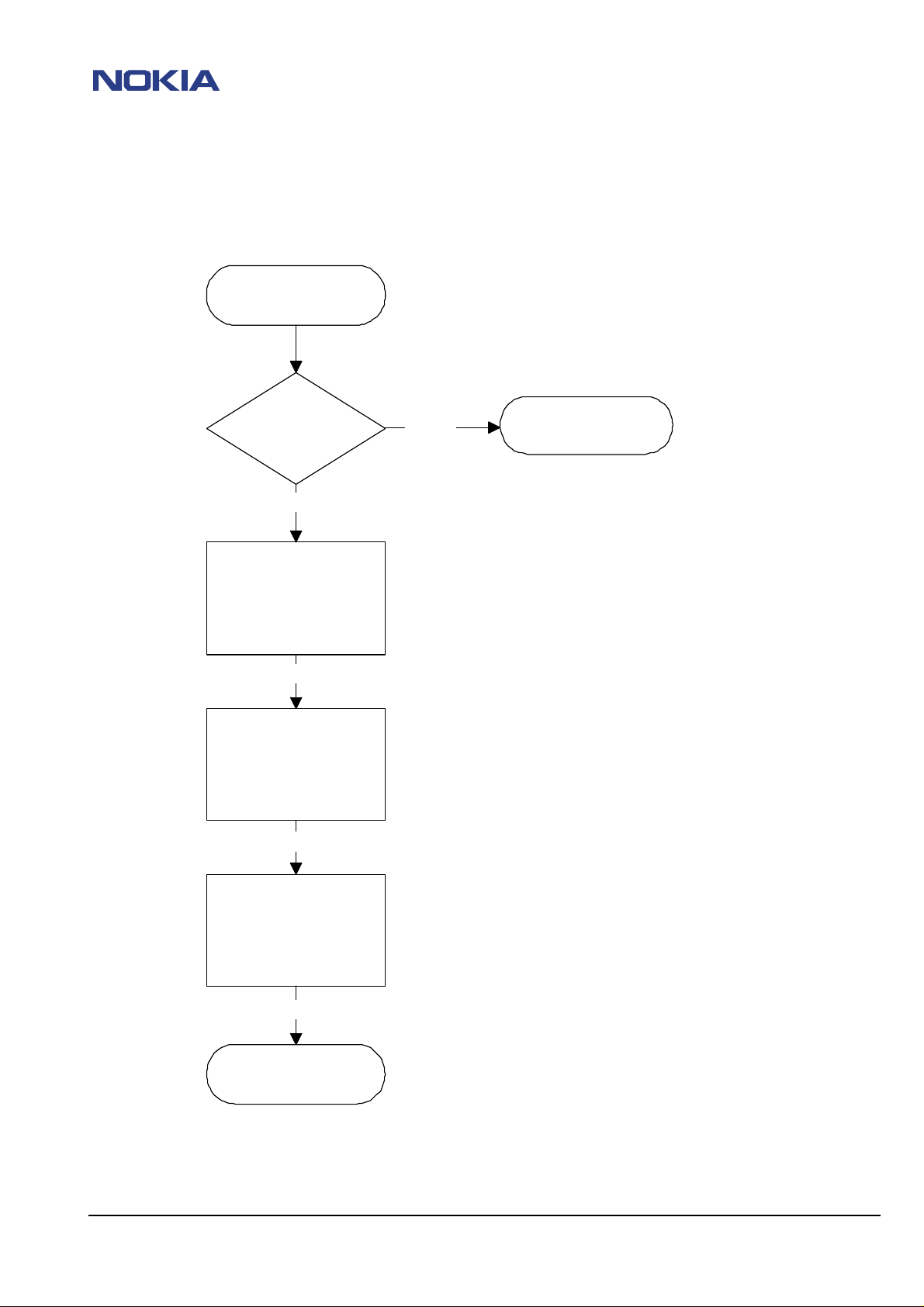
INSERT SIMCARD
Insert SIMcard
Check soldering and
contacts of X100
OK
Check signals at X100,
(see next page)
pin1 -SIMclk;
pin2 -SIMrst;
pin3;5 -VSIM;
pin6 -SIMdata
not OK
Change N100
not OK
not OK
Resolder or
change X100
Check lines to GND at
C116/129/130/131.
Values must be >100k
Also check R120
OK
D300 or PCB
faulty
Repairhints_nse5_002508 Checked by:
AMS TRAINING GROUP
Approved by:
SACE
Page 6
CONFIDENTIAL 6 (30)
NSE-5
Service & Analysis Center Europe Repairhints Version 1.0 Approved
SACE AMS Training Group 30.07.2000
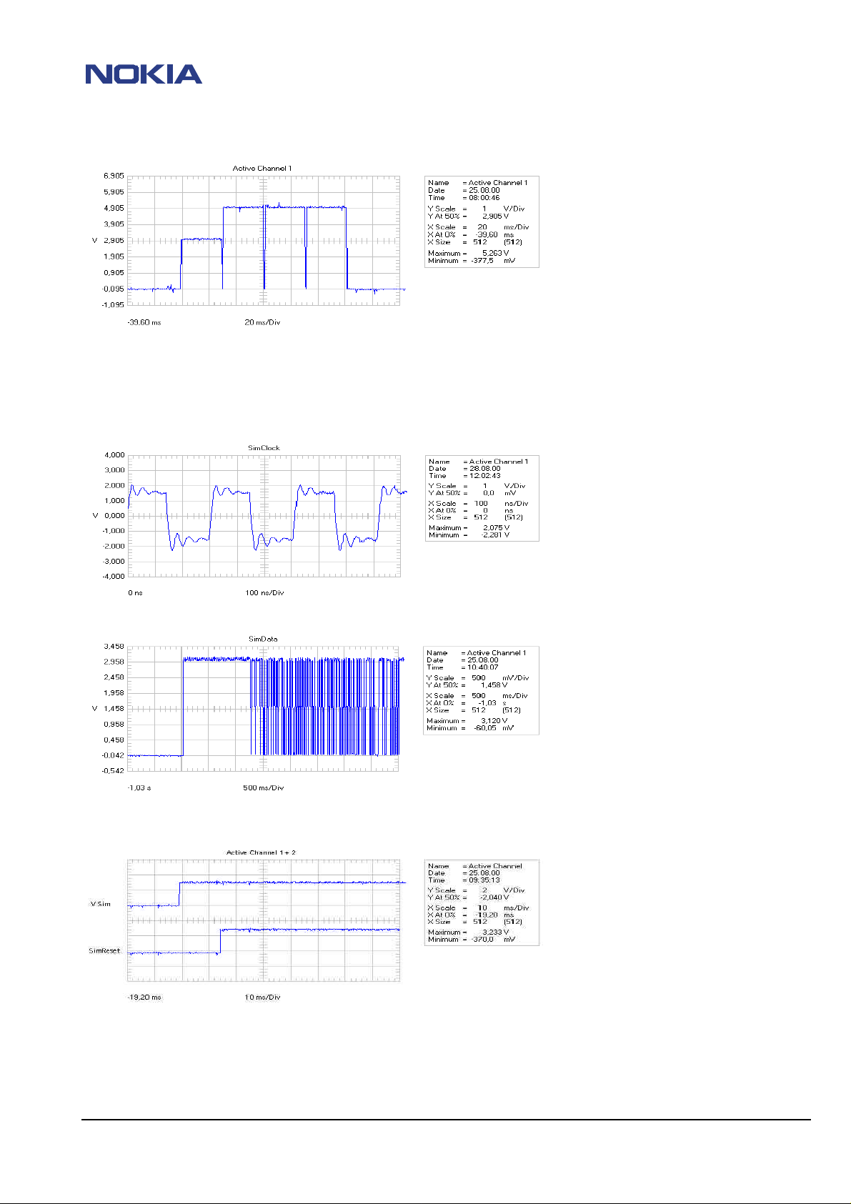
VSIM after switching on the phone without SIMcard. CCONT pulses up VSIM for four times, the first
time the amplitude is 3 Volt, the next three times it is 5 Volt.
If the phone is switched on with SIMcard, VSIM stays on the level with which the SIMcard works,
expected that SIMcard is not dirty or damaged.
Note that SIMClock and SIMData are only present when SIMcard is active, for example when phone registers to
network.
SIMReset is low-active, that means that the SIMcard will be reseted when SIMReset is 0 Volt. This is the case after
switching on the phone (diagram above). While VSIM is already high, SIMReset keeps low for a few milliseconds – in
this time the card will be reseted.
Repairhints_nse5_002508 Checked by:
AMS TRAINING GROUP
Approved by:
SACE
Page 7
CONFIDENTIAL 7 (30)
NSE-5
Service & Analysis Center Europe Repairhints Version 1.0 Approved
SACE AMS Training Group 30.07.2000
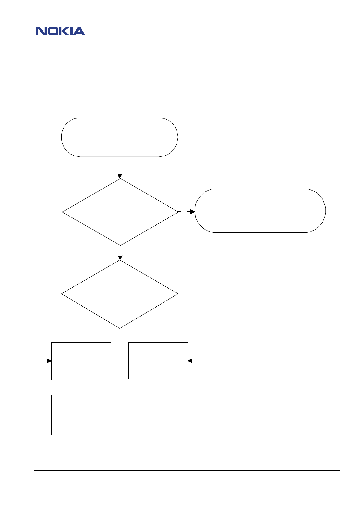
SIMCARD NOT ACCEPTED
"SIMCard not accepted" appears on
LCD
Use WinTesla to open
"QuickInfo"- window.
Compare shown SIMlock data with the
listed entries of the respective product code
notOK
Rewrite SIMlock settings with NOKIA
SECURITY PASSWORD or send phone to
notOK notOK
Change D301 if is
permitted to you to
SACE. If SIMlock is corrected or inactive, but
fault stays on- change COBBA* and rewrite
SIMlock data.
Send Phone to SACE if
it is not permitted to
rewrite IMEI
you to rewrite the IMEI
OK
SIMlock is OK.
If the MSIN data field is closed to a special IMSI
number range, only the operator is authorized to
open the SIMlock.
See General SB 065
*NOTE: If COBBA or D301 was changed, SIMlock & IMEI
data must be rewrite.
Also realign RX/TX values, especially TX I/Q !
Repairhints_nse5_002508 Checked by:
AMS TRAINING GROUP
Approved by:
SACE
Page 8

CONFIDENTIAL 8 (30)
NSE-5
Service & Analysis Center Europe Repairhints Version 1.0 Approved
SACE AMS Training Group 30.07.2000
X100 SIMcard Reader
- Check solderings of connector.
- Check if bend or soiled, change if necessary.
SIM lines shorts to GND
- Check resistance of SIM lines to GND at C116, C129, C130, C131,- value should be higher than
100kOhm.
- Check also R120.
N100 CCONT faulty
- Check SIMClock, SIMData, SIMReset and VSIM.
- It´s also possible that broken solderings under CCONT N100 are the reason for this fault. Remove CCONT,
tinplate oxidized pads carefully with only a little bit of flux and solder, replace CCONT with µBGA
rework machine.
N200 COBBA faulty
- If “SIM card not accepted” appears on LCD, but SIMlock-settings are ok or no SIMlock is set, it is
necessary to change COBBA N200.
Note that you have to rewrite SIMlock-data and tune Rx/Tx-values of the phone after changing the
COBBA,
Repairhints_nse5_002508 Checked by:
AMS TRAINING GROUP
Approved by:
SACE
Page 9
CONFIDENTIAL 9 (30)
NSE-5
Service & Analysis Center Europe Repairhints Version 1.0 Approved
SACE AMS Training Group 30.07.2000
PHONE DOESN`T SWITCH ON
Phone doesn`t switch on
Check VB 3,6VDC at C134
OK
PWRON at R413 drops to 0V while
pressing PWR Button
OK
32,768kHz squarewave at C150
~3,5Vpp.
OK
V_BB 2,8VDC at C139
OK
V_XO 2,8VDC at C112
OK
notOK
notOK
notOK
notOK
notOK
Change X101/102 if bend or
Check V_BB line for shorts to
GND. No shorts- change N100
Check V_XO line for shorts to
GND. No shorts- change N100
soiled.
Check L102
Change display assy.
Check R413
Change N100
V_REF 1,5VDC at C140
OK
PURX 2,8VDC at R147
OK
13MHz RFCLK at R301
OK
Try to flash the phone
notOK
notOK
notOK
Check V_REF line for shorts to
GND. No shorts- change N100
Check values around G701.
Continue with section "FLASH
Repairhints_nse5_002508 Checked by:
AMS TRAINING GROUP
Change N100
Change G701, use code
4510217, not 4510229
NOT POSSIBLE"
Approved by:
SACE
Page 10

CONFIDENTIAL 10 (30)
NSE-5
Service & Analysis Center Europe Repairhints Version 1.0 Approved
SACE AMS Training Group 30.07.2000
Battery connector X101, X102
- Check solderings of X101, X102.
- Check if connectors are bend or soiled.
Power on/off switch faulty
- Check that PWRON at R413 decreases to 0V during pressing the powerswitch.
- Check display connector X400, change display assy if necessary.
B100 problems
- Check voltage at B100, both Pins 1,6VDC.
- Check 32,768kHz sinewave signal level at C104.( 700mVpp).
- Check parts around B100 like R117, R118, R121, R135, C103, C104, C149.
- Check 32,768kHz squarewave at J318 (3,3Vpp).
G701 Reference oscillator faulty
- Check Vcc 2,8V at G701.
- Check Vcont ( may vary between 1 and 3.5V ).
- note that it is necessary to change G701 if frequency error is higher than 50Hz.
N100 CCONT faulty
- Check Vb 3,6Vat C134.
- Check that PWRON decreases to 0V at R413 when powerswitch is pressed.
- Check 32,768kHz squarewave at J318.
- Check 13MHz Clk-frequency at R301.
- Check Vbb 2,8V at C139.
- Check Vxo 2,8V at C112.
- Check Vref 1,5V at C140.
- Check PURX 2,8V at R147.
- Probably broken solderings under CCONT. Try to tinplate the oxidized pads careful with only a little bit
of flux and solder.
D300 MAD faulty
- Check 32,768kHz squarewave at J318.
- Check 13MHz Clk-frequency at R301.
- Check Vbb 2,8V at C139.
- Check PURX 2,8V at R147.
- MAD is probably faulty, swap the phone because MAD is not changeable.
Repairhints_nse5_002508 Checked by:
AMS TRAINING GROUP
Approved by:
SACE
Page 11

CONFIDENTIAL 11 (30)
NSE-5
Service & Analysis Center Europe Repairhints Version 1.0 Approved
SACE AMS Training Group 30.07.2000
FLASH UPDATE NOT POSSIBLE
Phone doesn`t switch
on: Flash update not
possible
Check if fault code from
prommer is one of the
YES NO
following: MCU boot failure,
serial data line failure, serial
clock line failure
Resolder RAM or
change if necessary. Try
to update again
Any message
No message
Phone is OK
YES
External RAM fault
Change Flash D303, try
to update again
No message
Phone is OK
No
Yes
Any message
Algorithm code
fail, alias ID
missing
notOK
Update FPS4 BOX
with the latest
flash device file
Next step only if it is permitted
to you to rewrite IMEI,
otherwise send phone to SACE
Change Flash D301, try
to update again
Connect "watchdog disable"
R413, -see layout- to GND
Check VBB 2,8VDC at
C139, Vxo 2,8VDC at
C112
OK
Check PURX at R147,
2,8VDC
OK
Continue next page
notOK
notOK
Any message
Change SDRAM or
swap, probably MAD or
PCB defect
It`s now necessary to
Continue with section
CCONT
make full factory set,
rewrite IMEI phone data,
update once again
Check 32,768kHz squarewave
signal at C150 approximately
600mV. If not OK, check
periphery of B100, Change
B100 or N100 if necessary
NOTE : If COBBA or D301 has been changed, SIMLOCK & IMEI
data have to be rewritten. Also realign RX/TX values,
especially TX I/Q !
Repairhints_nse5_002508 Checked by:
AMS TRAINING GROUP
Approved by:
SACE
Page 12

CONFIDENTIAL 12 (30)
NSE-5
Service & Analysis Center Europe Repairhints Version 1.0 Approved
SACE AMS Training Group 30.07.2000
FLASH UPDATE NOT POSSIBLE - CONTINUE –
Phone doesn`t switch on-
continue
notOK
Check 13MHz CLK frequency
at R301
OK
Check the resistance of following lines:
MBUS - X200 pin 11 to V102,pin 4.
FBUS RX - X200 pin 12 to V101,pin 5
FBUS TX - X200 pin 13 to V101,pin4
OK
No message
Check R106/304/306,
V101/102.
Try to update again.
Fail
No message
Change D304/305/306, try
to update again
Fail
No message
Change D303, try to update
again
notOK
Check 13MHz at G701,
change if necessary
OK
Check V702 and accessory
parts
Phone is OK
Phone is OK
Phone is OK
notOK
notOK
Check VCC at G701 (2,8V)
OK
Change G701
Change N100
notOK
PCB faulty
Contact service
Next step only if it is permitted
to you to rewrite IMEI,
otherwise send phone to SACE
Change D301, try to update
again
Fail
Probably MAD or PCB is
faulty
Repairhints_nse5_002508 Checked by:
OK
Rewrite IMEI & phone data,
update once again
NOTE : If COBBA or D301 has been changed, SIMLOCK & IMEI
data have to be rewritten. Also realign RX/TX values,
especially TX I/Q !
AMS TRAINING GROUP
Approved by:
SACE
Page 13

CONFIDENTIAL 13 (30)
NOTE: If COBBA or D301 has been changed, SIMLOCK & IMEI data must be set.
NSE-5
Service & Analysis Center Europe Repairhints Version 1.0 Approved
SACE AMS Training Group 30.07.2000
CONTACT SERVICE PROBLEMS
Note: If the Phone displays “ Contact Service “, Check with WinTesla which kind of selftest fails.
Before open the phone, try to flash it in every case of selftest failure.
In most of these cases, it would be possible to “repair” the phone or find out
more about that failure.
Possible failures with message “Contact Service”:
MCU ROM Checksum failed:
Try to flash the phone. If the failure persists, change D303.
RTC battery failed:
Change RTC battery and charge it, change N100 if failure persists.
(Charging RTC battery : Assemble phone and leave battery10 Minutes on it).
CCONT interface failed
Change CCONT (N100), (broken soldering).
DSP alive test failed:
Change COBBA. If failure persists, MAD should be the reason.
(Swap, because MAD is not changeable).
COBBA serial or parallel failed:
Change COBBA.
Warranty State failed:
Eeprom Data mismatch or phone is locked after swap process- send Phone to SACE.
If the Phone response any EEPROM mismatch ( PPM Validity ), Checksum failure or EEPROM failure,
- (D301) is faulty.
When your phone response a current consumption for empty Flash (~30mA) and doesn`t switch on
after a succesful update with WinTesla, D301 is faulty.
Message : Factory default values cannot be set – D301 is faulty.
Also realign RX/TX values, especially TX I/Q. Never change D301 if you have no
permission to rewrite IMEI. In case of this send phone to SACE.
Repairhints_nse5_002508 Checked by:
AMS TRAINING GROUP
Approved by:
SACE
Page 14

CONFIDENTIAL 14 (30)
NSE-5
Service & Analysis Center Europe Repairhints Version 1.0 Approved
SACE AMS Training Group 30.07.2000
NOT CHARGING ( NOTHING HAPPENS IF CHARGER IS CONNECTED )
First of all : Always Check the mechanical condition of all connectors and connections
Not charging
Check voltage level at R104-
if it is higher than 0,4V when
charger is connected
>0,4V
lower 0,4V
Check/change R102/103/104,
F100, X101/102/200,
N101, C101/144,R101 (soldering,
electrical and mechanical
condition)
OK
PCB faulty
Check/change N100
notOK
Repairhints_nse5_002508 Checked by:
AMS TRAINING GROUP
Approved by:
SACE
Page 15

CONFIDENTIAL 15 (30)
NSE-5
Service & Analysis Center Europe Repairhints Version 1.0 Approved
SACE AMS Training Group 30.07.2000
NOT CHARGING (APPEARS IN DISPLAY,- & ERRORBEEP)
"Not charging" -appears
on display-& errorbeep
notOK
Failure
messages
Energy management
calibration
Battery temperature
failed
Battery size failed
Battery voltage failed
Charge current failed
OK
not OK
not OK
not OK
not OK
Try to charge after
calibration
Check X101 values at
R115/123. Change N100
Check X102 values at
R115/123. Change N100
Change N100
Check R102, change
N100/101
Charge voltage failed
Check V_CHAR on voltage
devider R103/104
not OK
OK
Change N100
Repairhints_nse5_002508 Checked by:
AMS TRAINING GROUP
Check F100,R100, change
N101
Approved by:
SACE
Page 16

CONFIDENTIAL 16 (30)
NSE-5
Service & Analysis Center Europe Repairhints Version 1.0 Approved
SACE AMS Training Group 30.07.2000
X101, X102 Battery connector, X200 system connector
- Check soldering of connectors.
- Check mechanical appearance of connectors, change if necessary.
F101 faulty
- Check resistance of F101 (0 Ohm)
V_In line short circuit to GND
- Check resistance of V_In line to GND (~50 kOhm).
- if resistance is not ok Check R101 / C101 / C144 or change N101.
N100 faulty
- Change CCONT / N100 if any A/D value is out of limits but DC voltage is ok.
- If DC voltages are not ok Check corresponding voltage dividers and battery connectors X101/102.
- Probably broken solderings under CCONT / N100. Remove CCONT, tinplate oxidized pads carefully with flux
and solder, replace sparepart with µBGA rework machine.
Energy management calibration
- Run calibration if charging stops too early.
- If message “not charging“ appears on LCD.
- If any part in the charging circuit has been replaced.
Repairhints_nse5_002508 Checked by:
AMS TRAINING GROUP
Approved by:
SACE
Page 17

CONFIDENTIAL 17 (30)
NSE-5
Service & Analysis Center Europe Repairhints Version 1.0 Approved
SACE AMS Training Group 30.07.2000
NO SERVICE GSM 900 - First Check spectrum if it is only a RX failure , see spectrum charts.
REF: GSM 900: Ch60 (947 MHz) / GSM 1800: Ch700 (1842,8 MHz).
WINTESLA TUNING RX CALIBRATIONS
Failed to set low
reference
Change Z700
Change Z701
notOK
notOK
Failed to set
high reference
Check 71 MHz
IF at C617/618
OK
Check 71 MHz
IF at
N700,pin37/38
OK
Check 13MHz
IF in/out at
Z701
notOK
Check 13MHz
Ref.frequency at
G701,N700, pin15
(+/- 50Hz)
OK
Check GSM
LNA 947MHz
at N600,pin27
OK
Check 947
MHz in/out at
Z600
notOK
Change G701
notOK
Check
Z500/503
notOK
Change Z600
OK
Check UHF
2036 MHz at
N600 Pin3
OK
Check UHF
2036 MHz at
G700
Change N700
notOK
OK
Check 13MHz
IF at N700 pin
23/24
OK
Change COBBA
( N200 )
OK
notOK
NOTE : If COBBA has been changed, SIMLOCK & IMEI
data must be set. Also realign RX/TX values esp.TX
I/Q.
Repairhints_nse5_002508 Checked by:
Check Vc&Vcc
at G700
AMS TRAINING GROUP
notOK
Change N600
notOK
Change G700
Approved by:
SACE
Page 18

CONFIDENTIAL 18 (30)
NSE-5
Service & Analysis Center Europe Repairhints Version 1.0 Approved
SACE AMS Training Group 30.07.2000
NO SERVICE GSM 1800 First Check spectrum if it is only a RX failure. See spectrum charts.
REF: GSM 900: Ch60 (947 MHz) / GSM 1800: Ch700 (1842,8 MHz).
WINTESLA TUNING RX CALIBRATIONS
Failed to set low
reference
notOK
Check Z501 ( if bend or
defect )
Change Z501
OK
Check PCN_LNA at
N600,pin34
OK
Check 1842,8 MHz
in/out at Z602
OK
Check 13 MHz RFCLK
OK
Check UHF 2029,8MHz
at G700 and N600,pin3
OK
Check IF 187MHz at
N600,pin45/46
OK
Check 1/4 VHF 116 MHz
at N600,pin9
notOK
notOK
notOK
notOK
notOK
notOK
OK
Check PCN_LNA at
Z504, Z503, X501, X500
Change Z602
Change G701
Change G700
Change N600
Check 71MHz IF at
C617/618
OK
Check 71MHz IF at
N700,pin37/38
OK
notOK
notOK
Change N700
Change Z700
Check values at N700
and G702
Check 13MHz IF at
Z701,in/out
OK
Check 13MHz IF at
N700,pin23/24
OK
Change COBBA
notOK
notOK
Repairhints_nse5_002508 Checked by:
AMS TRAINING GROUP
Change Z701
Change N700
Approved by:
SACE
Page 19

CONFIDENTIAL 19 (30)
NSE-5
Service & Analysis Center Europe Repairhints Version 1.0 Approved
SACE AMS Training Group 30.07.2000
POOR / NO SERVICE -GSM 900 / GSM 1800
RSSI Measurement Failure messages.
REFERENCE IS : CH60-947 MHZ FOR GSM 900 AND CH700-1842,8 MHZ FOR GSM 1800.
IF THERE IS ONE OF THE FOLLOWING FAILURE MESSAGES, CHECK ALSO TX–SPECTRUM.
IF IT IS ONLY RF FAULT – OR USE CCONT CHAPTER AND SEE SPECTRUM SAMPLES.
CAN´T SET HIGH REFERENCE / CAN´T SET LOW REFERENCE AT GSM 900
Check 71 MHz IF at C617 / C618 --- If not ok – Check 13 MHz Ref. Freq. at G701.
Check 71 MHz IF at N700 / Pin 37,38 --- If not ok – change Z700.
Check 13 MHz IF at Z701 in & out ( 5dB attenuation over ) --- If not ok – change Z701.
Check 13 MHz at N700 / Pin 23,24 --- If not ok – change N700.
Check GSM_LNA 947 MHz at N600 / Pin 27 --- If not ok check / change Z500 / Z503.
Check GSM_LNA 947 MHz at Z600 in & out --- If not ok – change Z600.
Check UHF Oscillator Freq. 2036 MHz at N600 / Pin 3 --- If not ok – change N600.
Check UHF Oscillator Freq. 2036 MHz at G700 ( and VC/VCC ) --- If not ok – change G700.
Change N200 ( COBBA ).
NOTE: IF COBBA HAS BEEN CHANGED, IT IS NECESSARY TO REWRITE IMEI AND SIMLOCK DATA .
ALSO RX / TX - AND TX I/Q - VALUES MUST BE REALIGNED.
CAN`T SET LOW REFERENCE AT GSM 1800
Check if Z501 is bend --- change if necessary.
Check PCN_LNA 1842,8 MHz at N600 / Pin 34-If not ok -ckeck Signal at Z504/503 and X501/500.
Check PCN_LNA 1842,8 MHz at Z602 in & out --- If not ok change Z602.
Check UHF Oscillator Freq. 2029,8 MHz at N600 / Pin 3 --- If not ok – change G700.
Check 187 MHz IF at N600 / Pin 45,46 --- If not ok – change N600.
Check 116 MHz (1/4 VHF) at N600 / Pin 9 --- If not ok – check Values at N700 and G702.
Check 71 MHz IF at C617 / C618 --- If not ok – check 13 MHz Ref. Freq. at G701.
Check 71 MHz IF at N700 / Pin 37,38 --- If not ok – change Z700.
Check 13 MHz IF at Z701 in & out ( 5dB attenuation ) --- If not ok – change Z701.
Check 13 MHz at N700 / Pin 23,24 --- If not ok – change N700.
Check GSM_LNA 947 MHz at N600 / Pin 27 --- If not ok check / change Z500 / Z503.
Check GSM_LNA 947 MHz at Z600 in & out --- If not ok – change Z600.
Check UHF Oscillator Freq. 2036 MHz at N600 / Pin 3 --- If not ok – change N600.
Check UHF Oscillator Freq. 2036 MHz at G700 ( and VC/VCC ) --- If not ok – change G700.
Change N200 ( COBBA ).
NOTE: IF COBBA HAS BEEN CHANGED, IT IS NECESSARY TO REWRITE IMEI AND SIMLOCK DATA
ALSO RX / TX - AND TX I/Q - VALUES MUST BE REALIGNED.
Repairhints_nse5_002508 Checked by:
AMS TRAINING GROUP
Approved by:
SACE
Page 20

CONFIDENTIAL 20 (30)
NSE-5
Service & Analysis Center Europe Repairhints Version 1.0 Approved
SACE AMS Training Group 30.07.2000
Faulty spectrum – COBBA faulty, COBBA and CCONT broken soldering.
1) 3)
2) 4)
Pic1) Normal Spectrum
Pic2) Spectrum with broken soldering under CCONT
(No PCN_low reference settings in RSSI alignment).
Spectrum turnes to pic1 if N100 is pushed carefully with some nonmetaled item. This fault can
also be measured at N700 pin 15.(13MHz RFCLK).
Pic3) Spectrum with faulty COBBA, RSSI-alignment is not possible.
Pic4) Spectrum with broken soldering under COBBA, RSSI- alignment is not possible. Spectrum turnes
To pic 1 if N200 is pushed carefully with some nonmetallic item.
Repairhints_nse5_002508 Checked by:
AMS TRAINING GROUP
Approved by:
SACE
Page 21

CONFIDENTIAL 21 (30)
NSE-5
Service & Analysis Center Europe Repairhints Version 1.0 Approved
SACE AMS Training Group 30.07.2000
TX FAILURE
GSM 900 faulty GSM1800 faulty
OK
Check 116 MHz at
N700, pin 44/45
OK
Check 116 MHz at N600, pin
25/26
OK
Check UHF 2036 MHz
at N600, pin 4
OK
Check PA_GSM
(902MHz) at
N600,pin22
notOK notOK
notOK
notOK
Check 13MHz RFCLK at N700,
pin15 (+/-50Hz). Change if
faulty.
OK
Check VHF 464MHz at
N700, pin 8
Change N700
Check Z702
Check/change G700
Change N600
notOK
OK
notOK
notOK
notOK
Check 232MHz at
Check 232Mhz at
N600,pin 35/37
Check UHF 1979,8MHz
Check PA_PCN
(1747,8MHz)at
Change G702
N700,pin 46
OK
OK
at N600,pin4
OK
N600,pin 40
OK
Check
PA_GSM(902MHz) at
N500,pin1
OK
Check PA_GSM at
N500,pin4
OK
Check PA_GSM at L500,
Z500/503, X500/501
Change Z504
Check/change
a) N600, b) N100 (pin24)
if notOK, MAD faulty
notOK
notOK
YES
notOK
Check Z601 (in/out)
Check Z603,N502,Z502
Check at N500/501,pin2:
CTL_GSM=0,7-1,7Vpp
CTL_PCN=0,12-0,2Vpp
( squarewave, depends on PWR-level )
Check VC at Z504
(0,9VDC squarewave)
notOK
Check at N503: a).BAND_SEL
(lowlevel)on pin2, b).VTX
(2.8Vpulsed)on pin 1
notOK
notOK
OK
OK
Check PA_PCN at
N501,pin1
OK
Check PA_PCN at
N501,pin4
OK
Check PA_PCN at
Z504-Ant-conn.
notOK
Check/change L503
Check PA_PCN at Z503,
X500/501
Repairhints_nse5_002508 Checked by:
AMS TRAINING GROUP
Approved by:
SACE
Page 22

CONFIDENTIAL 22 (30)
NSE-5
Service & Analysis Center Europe Repairhints Version 1.0 Approved
SACE AMS Training Group 30.07.2000
2. TX - POWER FAULTS
3. TX FAULT AT GSM 900 REFERENCE IS : CH 60 / 902 MHZ
Check 13 MHz Reference Freq. output at G701 ( and VC / AFC Pins ) --- If not ok – change G701.
Check 13 MHz Reference Freq. at N700 / Pin 15 --- If not ok – change N700.
Check VHF Oscillator Freq. 464 MHz at N700 / Pin 8 --- If not ok,
check values at G 702 ( VC / VCC ) --- change Oscillator if necessary.
Check 116 MHz at N700 / Pin 44,45 --- If not ok – change N700.
Check 116 MHz at N600 / Pin 25,26.
Check UHF Oscillator Freq. 2036 MHz at N600 / Pin 4 --- If not ok – change G700.
Check PA_GSM 902 MHz at N600 / Pin 22 --- If not ok – change N600.
Check PA_GSM 902 MHz at N500 / Pin 1 --- If not ok – check / change Z601 in & out (if possible).
Check PA_GSM 902 MHz at N500 / Pin 4 --- If not ok,
check CTL_GSM at N500 / Pin 2 => 0,7 – 1,7 Vpp squarewave / depends on Powerlevel.
If this happens --- change N500.
Check PA_GSM 902 MHz at L500 in & out ( or if bend ) --- If not ok – change L500.
Check PA_GSM 902 MHz at Z503 ( input ) --- If not ok – change Z500 after lifting case.
Check PA_GSM 902 MHz at X500 / X501.
4. TX FAULT AT GSM 1800 REFERENCE IS : CH 700 / 1747,8 MHZ
Check 13 MHz Reference Freq. output at G701 ( and VC / AFC Pins ) --- If not ok – change G701.
Check 13 MHz Reference Freq. at N700 / Pin 15 --- If not ok – change N700.
Check 464 MHz at N700 / Pin 8 --- If not ok – change G702.
Check 232 MHz at N700 / Pin 46 --- If not ok – change N700.
Check 232 MHz at N600 / Pin 35,37 --- If not ok – check outputs at Z 702 / change if necessary.
Check UHF Oscillator Freq. 1979,8 MHz at N600 / Pin 4 --- If not ok,
check values at G 700 ( VC / VCC ) --- change Oscillator if necessary.
Check PA_PCN 1747,8 MHz at N600 / Pin 40 --- If not ok – change N600.
Check PA_PCN 1747,8 MHz at Z603 in ( at L 613 ) & out --- If not ok – change Z603.
Check PA_PCN 1747,8 MHz at N502 in ( Pin 1 ) & out ( Pin 4 ) --- If not ok – change N502.
Check PA_PCN 1747,8 MHz at Z502 in ( C 515 ) & out ( R513 ) --- If not ok – change Z502.
Check PA_PCN 1747,8 MHz at N501 / Pin 4 --- If not ok,
check CTL_PCN at N500 / Pin 2 => 0,12 – 0,2 Vpp squarewave / depends on Powerlevel
If this happens --- change N501.
Check PA_PCN 1747,8 MHz at L503 in & out ( or if bend ) --- If not ok change L503.
Check PA_PCN 1747,8 MHz at Z504 output (Pin Ant / Throughhole connection).
If output at Z504 not ok – change Z504.
Check VC ( 0,9 Vpp squarewave ) for Z504 (at C 507).
Check VTX ( 2,8 V pulsed ) at N503 / Pin 1 --- If not ok – change N100.
Check BAND_SEL ( low Level ) at N503 / Pin 2 --- If not ok – change N600.
If BAND_SEL and / or VTX not ok after changing N100 / N600 => probably MAD faulty
Check PA_PCN 1747,8 MHz at Z 503 / X501 / X500.
Repairhints_nse5_002508 Checked by:
AMS TRAINING GROUP
Approved by:
SACE
Page 23

CONFIDENTIAL 23 (30)
NSE-5
Service & Analysis Center Europe Repairhints Version 1.0 Approved
SACE AMS Training Group 30.07.2000
INTERNAL AUDIO FAILURE
No audio
( speaker )
Change speaker if bend or
soiled. Also check X400 ,
change display assy if
necessary
not OK
check connections C204
to C404, C203 to C405.
Also check for shorts to
GND
not OK
No audio
( mic )
Check Pogo pins
OK
Change slide and try again
not OK
Change N200,
probably D300
faulty
Check/change V100,
C180/181/117/121. Check
lines to GND ( >1k )
OK
Change N200,
probably D300
faulty
OK
Check internal contact
springs between Pogo pins
and PCB pads
OK
Check voltage at Z103
(around 1,8V DC) during
active mic
not OK
Check values around
V111
Repairhints_nse5_002508 Checked by:
AMS TRAINING GROUP
Approved by:
SACE
Page 24

CONFIDENTIAL 24 (30)
NSE-5
Service & Analysis Center Europe Repairhints Version 1.0 Approved
SACE AMS Training Group 30.07.2000
EXTERNAL AUDIO PROBLEMS
1) External mic problems (Xmic )
Check C158 ( if broken or bend )
In this case : Use a new RTC battery, the length of spring-connectors are
the reason for bending the capacitor.
Check X200 . This item must be clean. Also check the soldering of the MBUS- connectors.
Check Z100, V106 input and output.
Change COBBA, note : Rewriting of IMEI and SIMlock data is necessary after changing the COBBA!
If Error persists. Probably MAD or PCB is defect.
2) External ear problems (Xear)
Check X200 – contacts and soldering.
Check Z102.
Check R114, V107 input and output.
Check Vbb at R112 = 2,8V DC.
Change COBBA , note : Rewriting of IMEI and SIMlock data is necessary after changing COBBA!
If error persists, probably MAD or PCB is defect.
Repairhints_nse5_002508 Checked by:
AMS TRAINING GROUP
Approved by:
SACE
Page 25

CONFIDENTIAL 25 (30)
NSE-5
Service & Analysis Center Europe Repairhints Version 1.0 Approved
SACE AMS Training Group 30.07.2000
MICROPHONE DOES NOT WORK
-Also see SB 018 –
Note : First of all check the mechanical condition of the phone and slide for mechanical
damage or stuck. (PogoPins).
Probable reasons:
- Shorts between contact tracks and slideflex.
These shorts often occur at the end of the slide-cover (friction-dust).
If this happens, clean the flex with dustfree cloth, especially in the bottom corner.
- The Pogo pins in microphone housing get stuck. If this happens, change
A-Cover.
- Check the internal contact springs from Pogo-pins and their connector pads
on the PCB.
- Check impedance (~ 1,8k) , change slide cover if necessary.
- Check solderings of Z103/104, C106/107/132.
- Check signals (given over MPA-1 =audio test probe ) at V100 in & out.
- Check V_COBBA at V111 (2,8VDC).
- Check voltage ( during call ) at C117/121 ( 1,4VDC ) , at E100 ( 0,3V ), E101 ( 1,8V ).
- Change COBBA if all of the above works.
Rewriting of IMEI and SIMlock data is necessary after changing the COBBA!
- If the error persists, MAD or PCB should be the reason.
Repairhints_nse5_002508 Checked by:
AMS TRAINING GROUP
Approved by:
SACE
Page 26

CONFIDENTIAL 26 (30)
14)LCD RSTX (2,8V without Display)
NSE-5
Service & Analysis Center Europe Repairhints Version 1.0 Approved
SACE AMS Training Group 30.07.2000
SPEAKER DOES NOT WORK
1) Digital noise (TDMA) in speaker
Change slide – cover.
Change speaker.
2) No audio from speaker
Change speaker if necessary.
Check flex on display assy (bend or dirty).
Change display assy if necessary.
Check connections in EAR_P line - C204 to C404.
Check connections in EAR_N line - C203 to C405.
Both lines = 1,4V during call.
If one of the above fails – PCB faulty.
Check resistance between speaker lines and GND (>1 MOhm).
Probably MAD (D300) or PCB faulty.
1)Temp ( 1,5V )
2)LCD enabled ( 2,8V )
3)Ear P( 1,3-1,9V )
4)LCD ( 2,8V )
5)GEN SIO
6) Ear N ( 1,3-1,9V )
7)PWR_ON
8)Light
9)VB
10)GND
11)GND
12)VBB (2,8V)
13)GEN SIO
DISPLAY ASSY : EAR_N EAR_P
Repairhints_nse5_002508 Checked by:
AMS TRAINING GROUP
Approved by:
SACE
Page 27

CONFIDENTIAL 27 (30)
J401
J402
Roller_A
Roller_B
Roller_C
NSE-5
Service & Analysis Center Europe Repairhints Version 1.0 Approved
SACE AMS Training Group 30.07.2000
Rollerkey problems
Note : First of all check the mechanical funktionality.
Check the ESD & connector springs.
If scrollfunction failed, check R411 on PCB (broken or bend).
Cut the RTC battery holder or change the B-cover.
For more details see SB 012
Check connections between R409 and J400, R410 and J401, R412 and J402.
If one of these connections failed, swap PCB.
Check resistance of R407-R412.
If all resistors and connections are OK, probably MAD or PCB should be the reason.
J400
C400 C401 C402
10nF
Repairhints_nse5_002508 Checked by:
AMS TRAINING GROUP
Approved by:
SACE
Page 28

CONFIDENTIAL 28 (30)
NSE-5
Service & Analysis Center Europe Repairhints Version 1.0 Approved
SACE AMS Training Group 30.07.2000
Product-Codes NSE - 5 22-Aug-00
Product-Code SIM-Lock Data Operator
0501580 APAC - Basic
0501829 APAC - Basic
0502999 APAC - K
0503018 APAC - J
0503019 APAC - J
0503073 APAC - K
0503200 Euro - F
0503201 Euro - E
0503202 No SIM-Lock Euro - D
0503203 MCC & MNC 00101 Euro - C
0503204 MSIN 0000000001 Euro - B
0503205 Euro - G
0503276 Euro - D / Omnitel Pronto Italia
0503277 Euro - D / Telecom Italia Mobile
0503278 Euro - D / WIND
0503281 Euro - G / Amena
0503442 APAC - Basic
0503443 APAC - Basic
0503444 Euro - H
0503445 Euro - I
0503446 Euro - D ALS
0503510 Euro - A
0504406 Euro - H / KPN Orange
0504590 Euro - D / BLU S.p.A.
0504782 Euro - D / Vodafone Airtouch
0504819 APAC - C / Korea / China
0504848 Euro - D / TELSIM TEWAP
0504849 Euro - D / Turkcel / TUWAP
Repairhints_nse5_002508 Checked by:
AMS TRAINING GROUP
Approved by:
SACE
Page 29

CONFIDENTIAL 29 (30)
NSE-5
Service & Analysis Center Europe Repairhints Version 1.0 Approved
SACE AMS Training Group 30.07.2000
Product-Code SIM-Lock Data Operator
0503279 MCC & MNC 21407 MoviStar
MSIN ?????????? Euro - G
0503280 MCC & MNC 21401 Airtel WAP Conecta
MSIN ?????????? Euro - G
0503282 MCC & MNC 26001 Polcomtel SA-Plus GSM
NOT PRODUCED ANYMORE MSIN ?????????? Euro - I
0503976 MCC & MNC 20801 France Telecom / Itineris
NOT PRODUCED ANYMORE MSIN ?????????? Euro - D
0503978 MCC & MNC 23433 Orange UK
MSIN ?????????? Euro - O
0504302 MCC & MNC 21601 Pannon
MSIN ?????????? Euro - C
0504303 MCC & MNC 21630 Westel
MSIN ?????????? Euro - C
0504304 MCC & MNC 23203 MaxMobil
MSIN ?????????? Euro - D
0504305 MCC & MNC 20408 KPN Telecom
MSIN ?????????? Euro - H
0504330 MCC & MNC 23201 Mobilkom
MSIN ?????????? Euro - D
0504363 MCC & MNC 26003 PTK Centertel
MSIN ?????????? Euro - I
0504364 MCC & MNC 26806 TMN
MSIN ?????????? Euro - G
0504381 MCC & MNC 26801 Telecel
MSIN ?????????? Euro - G
0504405 MCC & MNC 23205 Austria Connect-One
MSIN ?????????? Euro - D
0504407 MCC & MNC 26002 PTC ERA gs
MSIN ?????????? Euro - I
0504480 MCC & MNC 23207 Tele.ring
MSIN ?????????? Euro - D
0504614 MCC & MNC 20801 France Telecom,Itineris
MSIN ?????????? Euro - D
0504618 MCC & MNC 26803 Optimus Telecomunicacoes S.A.
MSIN ?????????? Euro - G
0504749 MCC & MNC 23430 One 2 One
MSIN ?????????? Euro - D
0504770 MCC & MNC 26001 POLCOMTEL wapcol
MSIN ?????????? Euro - I
0504874 MCC & MNC 21630 Westel (WESWA)
MSIN ?????????? Euro - C
0505004 MCC & MNC 20420 Dutchtone Postpaid
MSIN ?????????? Euro - H
0505058 MCC & MNC 26803 Centertel
MSIN ?????????? Euro - I
0505173 MCC & MNC 26003 Optimus Telecomunicacoes S.A.
MSIN ?????????? Euro - G
Repairhints_nse5_002508 Checked by:
AMS TRAINING GROUP
Approved by:
SACE
Page 30

CONFIDENTIAL 30 (30)
NSE-5
Service & Analysis Center Europe Repairhints Version 1.0 Approved
SACE AMS Training Group 30.07.2000
CHANGE HISTORY
Originator Status Version Date Comment
Bernhard
Kleine-Frauns
Bernhard
Kleine-Frauns
Bernhard
Kleine-Frauns
Bernhard
Kleine-Frauns
Draft 0.1 16.08.2000 First draft version for the repair group
Draft 0.3 21.08.2000 Insert comments from repair team, add
“General Instructions”
Draft 0.5 23.08.2000 Insert comments from repair team, add
“Faulty spectrum chart”
Draft 0.7 24.08.2000 “Contact Service-problems”,description of TX
power fault and SIMcard faults added.
Bernhard
Kleine-Frauns
Bernhard
Kleine-Frauns
Draft 0.9 28.08.2000 Audio fault descriptions added
Approved 1.0 31.08.2000 SIMlock updated.
Repairhints_nse5_002508 Checked by:
AMS TRAINING GROUP
Approved by:
SACE
 Loading...