Page 1

nokia
Service & Analysis Center Europa
SACE AMS Training Group
CONFIDENTIAL
Quick Baseband Repair Hints
NSE-5
Modified : 05.06.2000
1(4)
Version 1.0 Approved
V15
1
5
E101E101
66
E100E100
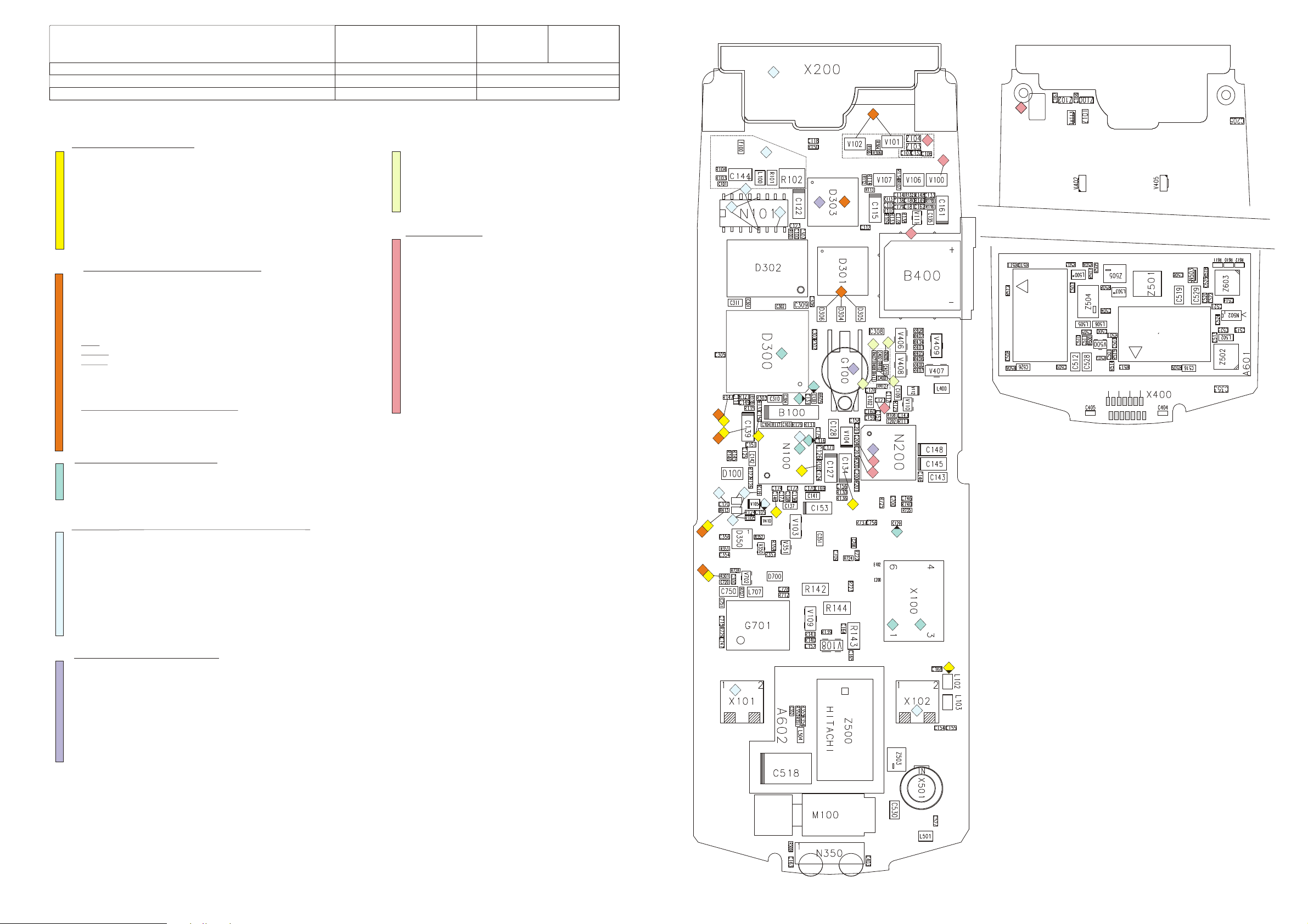
Phone doesn´t switch on (CCONT part)
1. Check Vb at C134. No, check connector X101/102. Change if bend or soiled. Also check L102.
2. Check if PWRON ( 3,6VDC ) at R413 drops to 0V during pressing the PWR-button. No, change
display assembly. Check R413.
3. Check 32,768 kHz squarewave signal at C150 - approximately 600mVpp.
Check/channgeC103/104/149, N100, B100
4. Check PURX at R147 ( 2,8VDC ) after pressing the PWR-button. No,- change N100.
5. Check VXO ( 2,8VDC at C112. No,- change N100, probably MAD or PCB faulty.
6. Check Vbb ( 2,8VDC ) at C139. No,- change N100 and check resistance to GND.
7. Check Vref ( 1,5VDC ) at C140. No,- change N100.
8. Check 13MHz CLK at R301. No,- check values at G701, change if necessary.
9. Try to flash the Phone. No,- continue with section Flash.
Doesn´t switch on, section: FLASH (update not possible)
A: Prommer-fault code : MCU boot failure, serial data line failure, serial clock line failure.
1. Disable watchdog by connecting R413 to ground.
2. Check Vbb ( 2,8V DC ) at C 139, Vxo ( 2,8V DC ) at C112, if not OK, continue with section Ccont.
3. Check PURX at R147 ( 2,8V DC ). If not OK, check 32.763 KHz squarewave signal at C 150
approxinately 600mV pp. No signal-check periphery of B100, change B100 or N100 if necessary.
4. Check 13 Mhz Clk frequency at R301, if not- check values at G701, change if necessary
5. Check lines :
MBUS-X200 pin 11 to V102 pin 4
FBUS_RX-X200 pin 12 to V101 pin 5
FBUS_TX-X200 pin 13 to V101 pin 4
[values should be around 100R, also check lines to ground for shorts.]
- Check R106,304,306,V101,V102 and try to update again.
6. Change D304,305,306,
7. Change D303 and try to update again. If not OK, probably Mad or PCB is faulty.
D301 should not be changed. ( Contains IMEI data. )
B: Prommer-fault code : External RAM fault
- Resolder RAM or change if necessary.
C: Algorithm code fail, alias ID missing
-. Update your FPS-4 Box with latest flash device list. If not OK, change D303.
Insert SIM card, SIM card not accepted
1. Check soldering and contacts of X100. Not ok- resolder or Change X100.
2. Check X100 pin 1 SIMclk; pin2 SIMrst; pin3/5 VSIM; pin6 SIMdata. Not ok- change N100
3. Check lines to GND of C116/129/130/131.Values must be >100k. Also check R120.
4. D300 or PCB faulty.
Not charging (NOTE: Always check the mechanical condition of connectors first )
A: Nothing happens if charger is connected
1. Check voltage level at R104, <0,4V if charger is connected. If not, check X101/102/200; F100; N101;
R101/102/103/104; C101/144 for soldering conditions or electrical defekts.
2. Check/Change N100
B:Display information and error beep
3. Check Voltage at C119is about 0,8V at PWR on and BSI value is 39K. If not, check/change X102;C119;
R123/115.
4. Check Voltage at C120 is about 0,5V at PWR on and Btemp=47k.If not, check/change X101;V105;
R105/124/115/123 C105/120.
5. Check 32KHz ( fast charge ) 1KHz ( slow charge ) at N101, pin 7. If not, check/change R100;N100;
C100;V102.
Roller-Key-problems
- Check the ESD&connector springs
1. Check R411 on PCB if broken or bend
2. Check connections R409-J400; R410-J401; R412-J402.
if one of these connections failed- swap PCB.
3. Check resistance of R407-R412.
- If all resistors and connections are ok, probably MAD or
PCB should be the reason.
Internal audio failure
A: Digital (TDMA) noise in speaker
-. Change slide-cover and/or speaker
B: Speaker does not work
- Check/change Speaker if necessary
- Check/change Display Assy
-. Check connectors at X400 and Display Assy ( see pinout diagrams )
1. Check connections in Ear-P-line- C204 ( BOT ) to C404 ( TOP )-(1,4V DC during call)
2. Check connections in Ear-N-line- C203 ( BOT ) to C405 ( TOP )-(1,4V DC during call)
- if one of the 2 above fails PCB is faulty.
- Resistance between speaker lines and ground must be >1meg.
- Probably D300 or PCB faulty
C: Microphone does not work
- Check impedance of mic ( 1800R ) if not, change slide-cover.
3. Check soldering of Z103/104, C106/107/132
4. Check signal ( audio-testprobe-MPA-1) at V100 in/out.
5. Check VCOBBA at V111 (2,8V DC)
6. Check (during call) at C117/121=1,4VDC; E100=0,3V; E101=1,8V
- Change COBBA if all of the above not works. If the error persits,
Mad or PCB should be the reason.
3
1
4
7
16
1
12
6
5
7
7
1
5
11
44
6
44
2
4
3
22
33
11
33
22
2
2
3
1
3
3
4
6
2
3
2
3
2
5
4
3
R115
4
R123
4
2
1
4
8
7
6
4
1
2
1
Pinout PCB connecting pads
1) Temp ( 1,5V )
2) LCD enabled ( 2,8V )
3) Ear P( 1,3-1,9V )
4) LCD ( 2,8V )
5) GEN SIO
6) Ear N ( 1,3-1,9V )
7) PWR_ON
3
1
2
1212
1414
1010
88
1313
1111
99
2233
11
5566
44
77
8) Light
9) VB
10) GND
11) GND
12) VBB (2,8V)
13) GEN SIO
14) LCD RSTX (2,8V without Display)
Contact Service, CCONT interface failed
First check with WinTesla, which is failed. Try to flash the phone.
.
MCU ROM checksum failed
1.Change D303
RTC Battery failed
2.Change RTC-battery,check/change N100
Ccont interface failed
3.Change N100 ( Black pads ? )
DSP alive test failed Cobba serial/parallel failed
4.Change Cobba,if not OK, - MAD defect.
Warranty state failed, PPM validation, or mismatch errors
-Eeprom data mismatch- sent phone to SACE, D301 contains IMEI Data, should not be changed.
Note: If COBBA was changed, it`s necessary to rewrite IMEI & Simlock Data, realign RX/TX & TX IQ
1
1
1
Page 2

nokia
Service & Analysis Center Europe
SACE AMS Training Group
CONFIDENTIAL
Quick RF-Part Repair Hints
NSE-5
Modified : 05.06.2000
2(4)
Version 1.0 Approved
V15
4
2
9
1
7
3
6
2
8
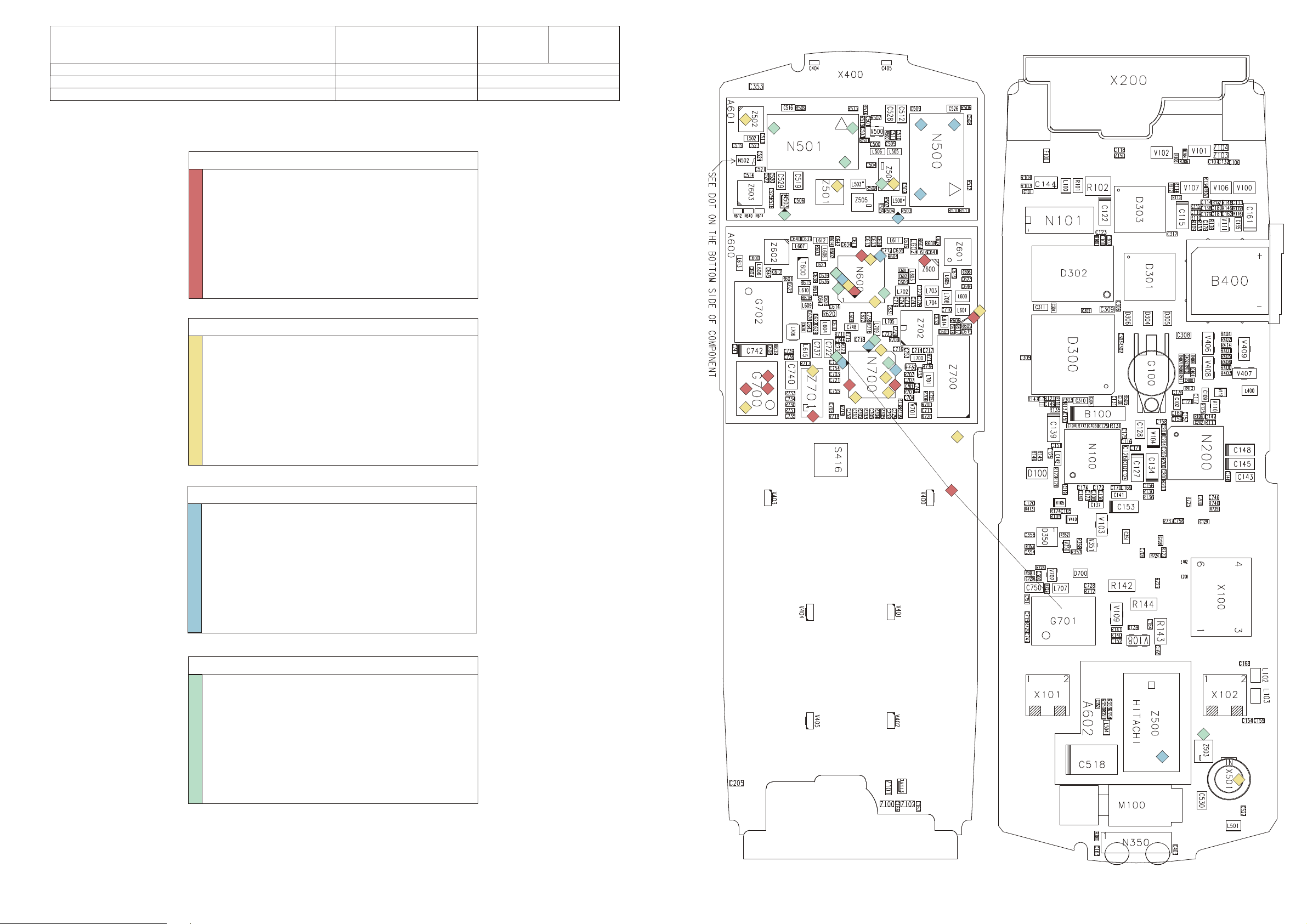
NO RX GSM900
1. Check IF2 71MHz at C617/618: No, goto 5
2. Check IF2 71MHz at N700 pin 37&38. No- change Z700
3. Check IF3 13MHz at Z701 in & out (~5dB attenuation). No- change Z701.
4. Check IF3 13MHz at N700 pin 23&24 : Yes- change COBBA, No-change
N700
5. Check 13MHz REF at G701 and N700 pin 15. No- change G701.
6. Check GSM_LNA (947MHz/Ch60) at N600 pin 27.No- Check/change
Z500/503.
7. Check GSM_LNA (947Mhz/Ch60) at Z600 in&out. No change Z600
8. Check UHF (2036MHz/Ch60) at N600 pin 3 No- change N600.
9. Check UHF (2036MHz/Ch60) at G700
10.Check Vc&Vcc at G700
11.Change G700
NO RX GSM1800
1. Check/change Z501 if bend or defekt .
2. Check PCN_LNA (1842,8MHz/Ch700) at N600 pin 34 : Yes, goto 5
3. Check PCN_LNA (1842,8MHz/Ch 700) at Z504/503 X501/500
4. Check PCN_LNA (1842,8MHz/Ch 700) at Z602 in&out .No-change Z600.
5. CheckUHF (2029,8MHz/Ch700) at G700. No- change G700.
6. Check UHF(2029,8MHz/Ch700) at N600 pin3. No- change N600.
7. Check IF1 (187MHz) at N600 pin 45&46. No- change N600.
8. Check 1/4 VHF (116MHz) at N600 pin 9
9. Check values at N700&G702.
10.Check IF2(71MHz) at C617/618. No- change N700.
11.Check IF2 (71MHz) at N700 pin 37&38.No- Change Z700
12.Check IF3 (13Mhz) at Z701 in&out.(~5dB attenuation) No- change Z701.
13.Check IF3 (13MHz) at N700 pin 23&24. No- change N700
14.Change COBBA
3 4
10
10
9
11
5
8
3
1
5
5
6
1
1
12
3
11
4
6
2
6
8
4
3
8
2
2
7
8
15
4
9
13
11
7
4
9
7
1
3
3
2
1
10
1
NO TX GSM900
1. Check 13MHz Reference Frequency at N700 pin 15 (max 50 Hz difference ).
No- change G701
2. Check 464MHz VHF at N700 pin8. No- change G702
3. Check 116MHz IF at N700 pin 44&45. No- change N700
4. Check 116MHz IF at N600 pin 25/26
5. Check UHF (2036MHz) at N600 pin3. No- change G700.
6. Check PA_GSM (902MHz/Ch60) at N500 pin1. No- change Z601
7. Check PA_GSM (902MHz/Ch60) at N500 pin 4. No- change N500
8. Check PA_GSM at N500 pin2 0,7-1,7Vpp ( depends on powerlevel )
9. Check PA_GSM at L500;Z500/503;X500/501
NO TX GSM1800
1. Check 13Mhz Reference Frequency at N700 pin 15. (max 50 Hz difference )
No- change G701
2. Check VHF 464Mhz at N700 pin 8. No- change G702
3. Check 232MHz IF at N700 pin46. No- change N700.
4. Check 232MHz IF at N600 pin 35 & 37. No, change/check Z702.
5. Check UHF (1979,8MHz/Ch700) at N600 pin3. No- change N600.
6. Check PA_PCN (1747,8/Ch700) at N600 pin 40. No- change N600.
7. Check PA_PCN (1747,8/Ch700) at N501 pin1. No- check/change Z602; N502; Z502.
8. Check PA_PCN (1747,8MHz/Ch700) at N501 pin4. Yes, check/change L503
9. Check PA_GSM at pin2/N501 0,12-0,2Vpp (depends on powerlevel).
10.Check at N503: Pin2 if Band-SEL (low level and
pin1-VTX (2,8V pulsed)
11.Check at Z504 pin 2 if it is 0,9V DC change Z504
12.Check PA_PCN at Z503/X500/501
5
12
9
3
Page 3

nokia
nokia
Service & Analysis Center Europa
Service & Analysis Center Europa
SACE AMS Training Group
SACE AMS Training Group
CONFIDENTIAL
CONFIDENTIAL
Colored Layout and Pinouts
NSE-5
NSE-5
Modified : 28.08.2000
3(4)
Version 1.0 Approved
V15
V15
100-199
200-299
300-399 700-799
400-499
500-599
600-699
Page 4

nokia
nokia
Service & Analysis Center Europa
Service & Analysis Center Europa
SACE AMS Training Group
SACE AMS Training Group
CONFIDENTIAL
CONFIDENTIAL
Measure Points
NSE-5
NSE-5
Modified : 28.08.2000
4(4)
Version 1.0 Approved
V15
V15
Ear_P to C204Ear_P to C204
Check if bendCheck if bend
Ear_N to C203Ear_N to C203
71MHz pin15/1671MHz pin15/16
VCVC
VHF outVHF out
2,7VDC2,7VDC
UHF outUHF out
GNDGND
13MHz IF in13MHz IF in
13MHz IF out13MHz IF out
GNDGND
V_SYN_2 ~2,7VDCV_SYN_2 ~2,7VDC
VCCVCC
FRACTRL pin 28FRACTRL pin 28
Roller B- R408/410Roller B- R408/410
Roller A- R407/409Roller A- R407/409
Roller C- R411/412Roller C- R411/412
SENApin7SENApin7
SLEEPCLK pin5SLEEPCLK pin5
CTL_GSM pin 31CTL_GSM pin 31
TXP pin 32TXP pin 32
J300J300
Slide (ROW 0) Slide (ROW 0)
S_DAT,pin6S_DAT,pin6
TXC
TXC
34
34
13MHz RFCLK13MHz RFCLK
J401J401
J400J400
J402J402
ROM 2 SEL XROM 2 SEL X
RP-pin34
RP-pin34
D301
D301
DSP XFDSP XF
71MHz IF71MHz IF
SleepCLK C111SleepCLK C111
GEN S_CLKGEN S_CLK
SIMCard IO Ctrl SIMCard IO Ctrl
SIMCard CLKSIMCard CLK
SIMCard res X SIMCard res X
SIMCard detSIMCard det
CCONT initCCONT init
SIMCard PWRSIMCard PWR
71MHZ71MHZ
Connect this side to
Connect this side to
GND to disable watchdog
GND to disable watchdog
J309J309
J307J307
J308J308
J318J318
J320J320
J322J322
J323J323
J324J324
J325J325
J101J101
J321J321
1
Fixing pads ( 2pcs )Fixing pads ( 2pcs )
1. V_IN
1. V_IN
2. L_GND
2. L_GND
3. V_IN
3. V_IN
4. CHRG_CTL
4. CHRG_CTL
5. CHRG_CTL
5. CHRG_CTL
6. Slide detect
6. Slide detect
PURXPURX
V_BBV_BB
PWR_ONPWR_ON
32KHz32KHz
V_REFV_REF
88
7
7. Slide detect GND
7. Slide detect GND
8. XMIC
8. XMIC
9. SGND
9. SGND
10.XEAR
10.XEAR
11.MBUS
11.MBUS
VxoVxo
VBVB
1414
MIC audio outMIC audio out
V_COBBA 2,8VDCV_COBBA 2,8VDC
CHECK THESE COMPONENTS
CHECK THESE COMPONENTS
( BEND ? )
( BEND ? )
Mic audio in Mic audio in
E100E100
E101E101
13MHz RFCLK13MHz RFCLK
GNDGND
VXOVXO
BTEMPBTEMP
GNDGND
V_CONTV_CONT
S_DATAS_DATA
SIM_CLKSIM_CLK
VSIMVSIM
SIMRSTSIMRST
BSIBSI
GNDGND
VSIMVSIM
V_BATTV_BATT
 Loading...