

Page 1

Nokia Customer Care
7088 (RM-219)
Mobile Terminal
Baseband Description and
Troubleshooting
Issue 1 12/2006 Company Confidential © 2006 Nokia Corporation
Page 2

7088 (Flower)
Base band Description and Troubleshooting
Contents Page
Introduction............................................................................................................... 4
Baseband and RF Architecture................................................................................ 5
Power Up and Reset................................................................................................ 6
Power Up.......................................................................................................8
Power Key..............................................................................................8
Charger...................................................................................................8
External supply source is detected.........................................................8
Power Off.......................................................................................................8
Power Consumption and Operation Modes...................................................9
Power-off Mode ......................................................................................9
Sleep Mode ............................................................................................9
Active Mode............................................................................................9
Charging Mode....................................................................................... 9
Power Distribution .................................................................................................. 10
Clock Distribution.................................................................................................... 11
TCXO...........................................................................................................12
SLEEP crystal circuit for 32.768 kHz...........................................................14
SBI CLK Interface........................................................................................15
Backend IC and Camera Module Clocks.....................................................16
Flash Programming Error Description.................................................................... 16
Charging Operation................................................................................................ 17
Battery .........................................................................................................17
Charging Circuitry........................................................................................17
Charger Detection........................................................................................18
Charge Control ............................................................................................19
Audio ...................................................................................................................... 19
Keypad ................................................................................................................... 21
Display.................................................................................................................... 21
Camera and Flash Light LED................................................................................. 22
Universal Serial Bus (USB).................................................................................... 22
Accessories............................................................................................................ 24
Charging......................................................................................................24
Headset Detection.......................................................................................24
Data Access.................................................................................................25
UIM CARD.............................................................................................................. 25
Page 2 © 2006 Nokia Corporation Company Confidential Issue 1 12/2006
Page 3

7088 (Flower)
Nokia Customer Care Baseband Description and Troubleshooting
Test Points.............................................................................................................. 26
Main Board Top Layer Test Points ...............................................................26
Main Board Bottom Layer Test Points..........................................................27
Sub Board Top Layer Test Points................................................................. 28
Sub Board Bottom Layer Test Points...........................................................29
Troubleshooting...................................................................................................... 30
Mobile Terminal is Dead............................................................................... 31
Flash Memory Faults ...................................................................................32
Power Does Not Stay ON or the Mobile Terminal is Jammed......................33
Charger Faults.............................................................................................34
Audio Faults.................................................................................................35
Display Faults..............................................................................................39
Keypad Faults..............................................................................................40
Keypad Faults..............................................................................................41
Camera Faults.............................................................................................42
Camera Faults.............................................................................................43
Issue 1 12/2006 © 2006 Nokia Corporation Company Confidential Page 3
Page 4

7088 (Flower)
Base band Description and Troubleshooting
Introduction
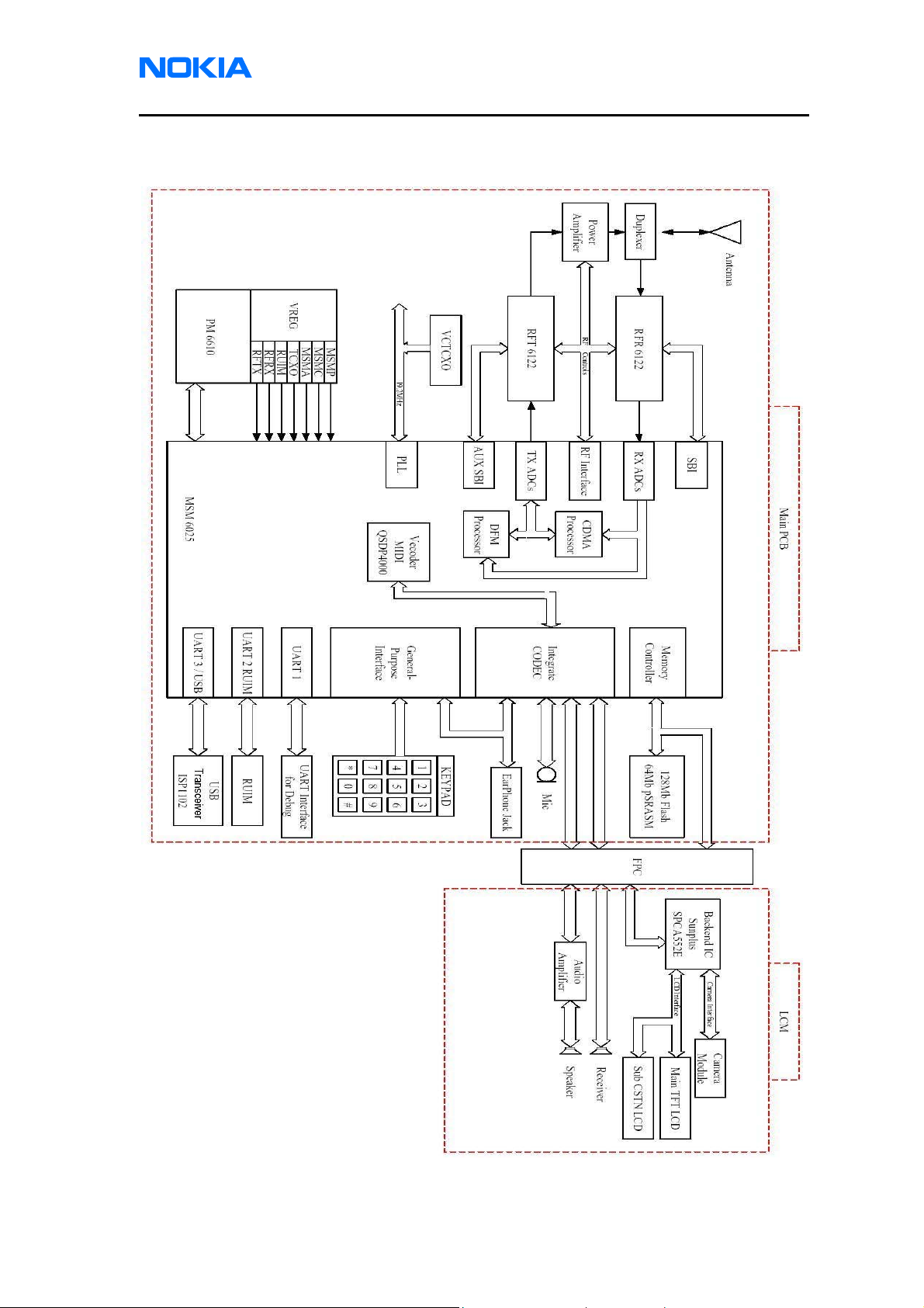
The mobile terminal with a CDMA single mode engine (Cellular/ 800) and Qualcomm
base band consists of the following ASICs:
Power Management IC, PM6610 (PM)
Mobile Station Modem processor, MSM6025 (MSM)
RFT6122 and RFR6122 are RF transmitter and receiver IC.
128Mb Flash memory and 64Mb pSRAM memory
Backend IC SPCA552E for image processing
The base band (MSM) is consisted of an ARM7 processor, a CDMA processor, a
DFM processor, QDSP & codec, PLL, analog interface for RF and controllers for
GPIOs, RUIM, USB & peripheral interfaces, all of which are necessary to complete
the entire CDMA base band system. ARM7 processor communicates with external
memory, backend IC and LCD through local address & memory buses. A QDSP4000
with codec inside the
processing/compression for microphone, receiver (earpiece) and speaker signals.
CDMA and DFM processors handle CDMA operation and control the radio chip
RFT6122 and RFR6122 through analog interface along with other digital control pins.
The RFT6122 and RFR6122 provide direct conversion of RF signal (zero IF)
architecture to support the CDMA2000 1X standard. The PM6610 controls the power
management for base band & RF system, and battery charging algorithm.
The base band architecture supports the power-saving function called “sleep mode”.
Sleep mode shuts off the voltage-controlled temperature-compensated crystal
oscillator (TCXO), which is used as the system clock source for both the RF and the
base band. During sleep mode, the system runs from a 32 kHz crystal and all the RF
regulators (VREG_RFTX, VREG_RFRX) are off. The sleep time is determined by
network parameters. Sleep mode is entered when both the Mobile Station Modem
(MSM) and its internal DSP are in standby mode and the normal TCXO clock is
switched off. The mobile terminal is awakened by a timer running from this 32 kHz
clock supply. The period of the sleep/ wake up cycle (slotted cycle) is 1.28N seconds,
where N=0, 1, 2, depending on the clot cycle index.
Mobile Station Modem (MSM) handles the voice
The mobile terminal supports standard Nokia 2-wire and 3 wire chargers (AC-3, AC-4,
DC-4, AC-5, ACP-12, AC-1). However, the 3-wire chargers are treated as 2-wire
chargers. The PWM control signal for controlling the 3-wire charger is ignored.
The MSM and PM energy management software control the charging.
BL-4B (700 mAh) lithium-ion battery is used as the main power source.
Page 4 © 2006 Nokia Corporation Company Confidential Issue 1 12/2006
Page 5
7088 (Flower)
Nokia Customer Care Baseband Description and Troubleshooting
Baseband and RF Architecture
Figure 1: Baseband and RF Block Diagram
Issue 1 12/2006 © 2006 Nokia Corporation Company Confidential Page 5
Page 6
7088 (Flower)
Base band Description and Troubleshooting
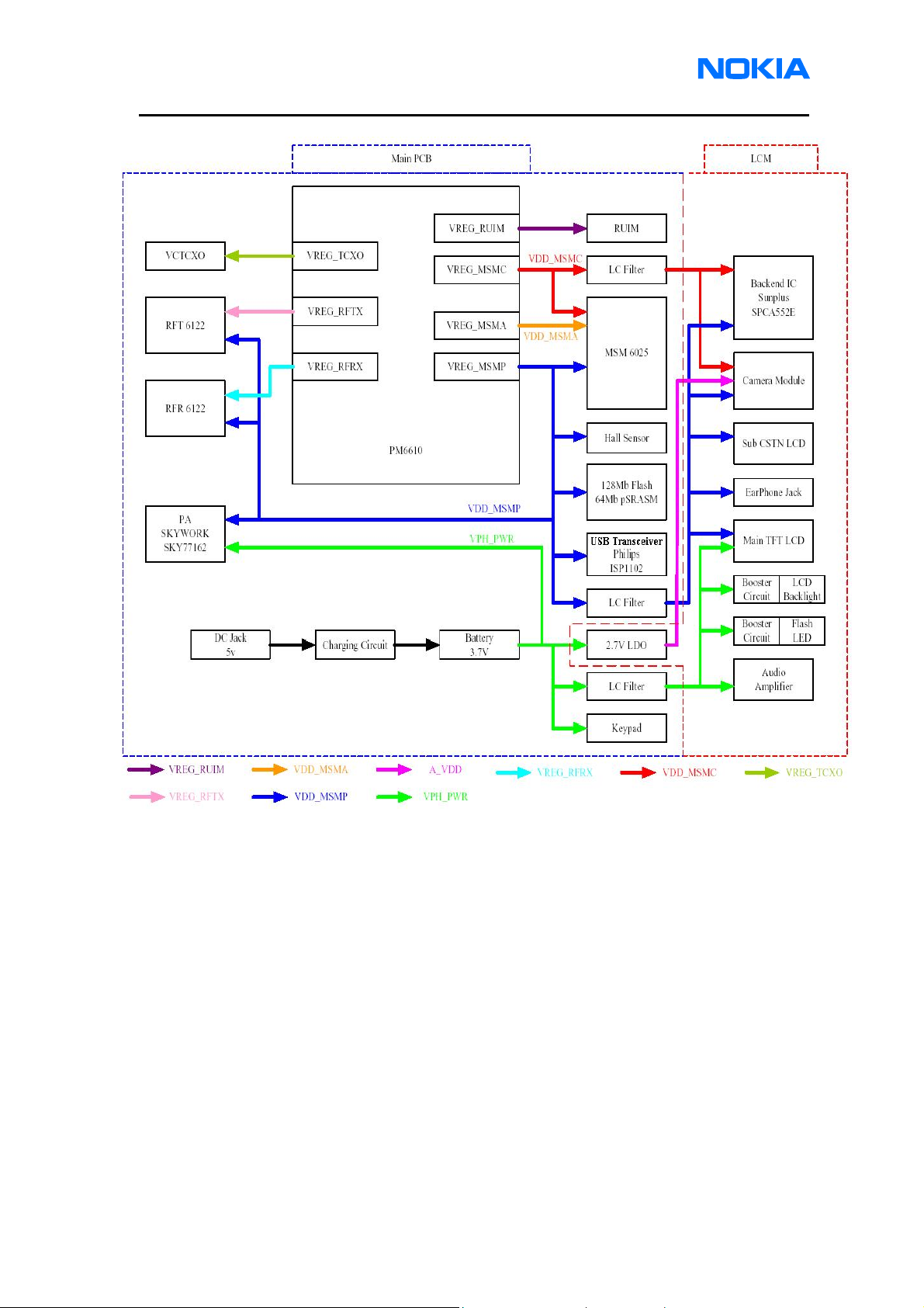
Figure 2: Power Distribution
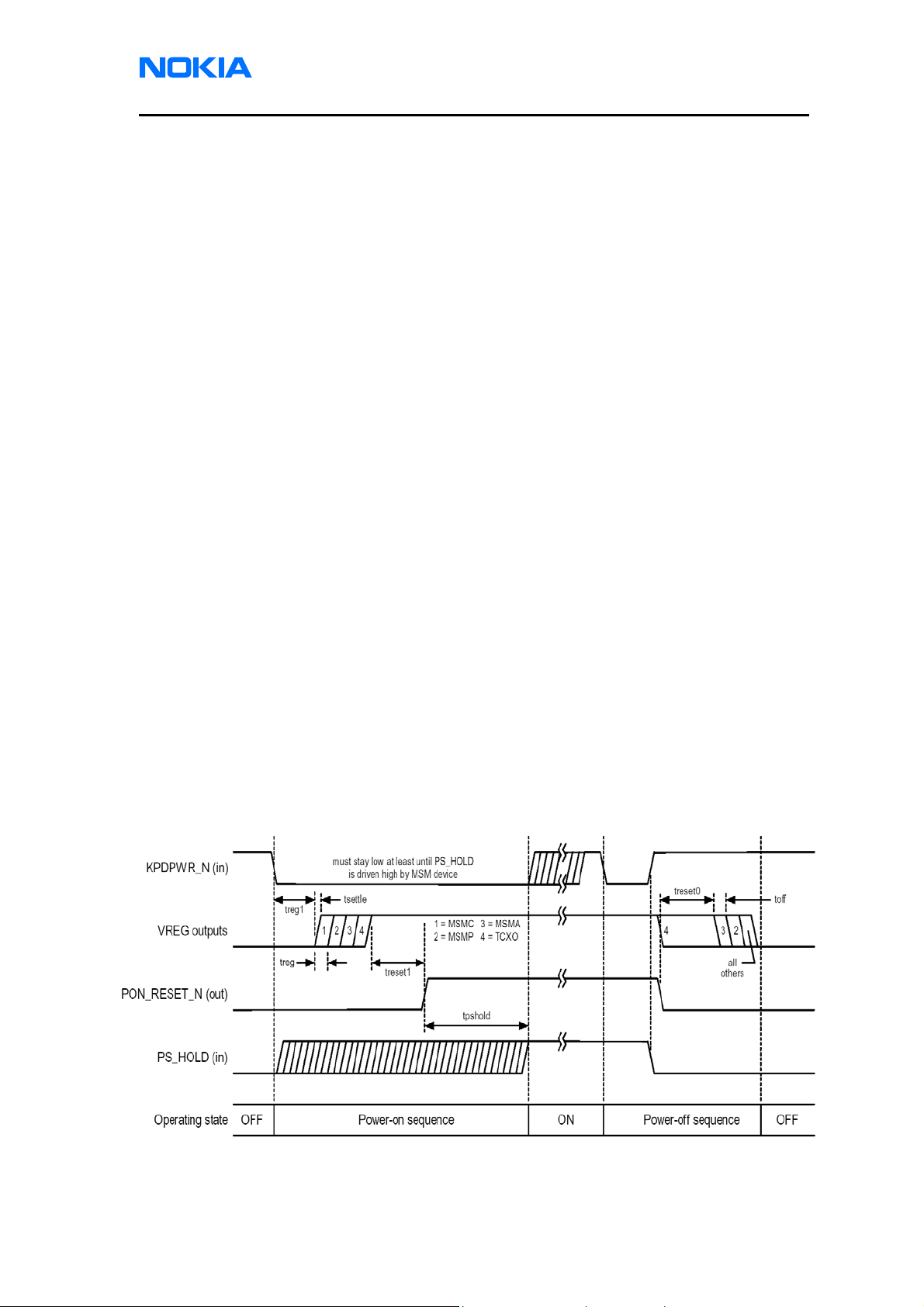
Power Up and Reset
The PM6610 ASIC controls the power up and reset. The base band (MSM) can be
powered up in the following ways:
Pressing the Power button, which means to ground the KPADPWR_N pin
of the PM (“PHONE_ON” net in schematic).
Connecting the charger to the charger input.
After receiving one of the above signals, the PM will start to enter reset mode. The
watchdog starts, and if the battery voltage is greater than its threshold, (3V), a 6ms
delay starts to allow MSM to settle. After this delay elapses, the VERG_MSMC
Page 6 © 2006 Nokia Corporation Company Confidential Issue 1 12/2006
Page 7
7088 (Flower)
Nokia Customer Care Baseband Description and Troubleshooting
regulator is enabled. Then, VERG_MSMP, VERG_MSMA & VERG_TCXO regulators
are enabled in sequence after MSMC. There is a 120us (4 Sleep Clocks) delays
between each regulator’s turning-on. The RESET_N signal (from PM6610 pin
“PON_RESET_N” to MSM6025 pin “RESIN_N” in schematic) holds low for another
20ms and is sent to MSM. Resets are generated for the MSM’s internal MCU and its
internal DSP, and MSM sends TCXO_ON signal to PM (“TCXO_EN” pin) to enable
TCXO. After RESET_N goes high, MSM holds PS_HOLD at low state for 200ms and
then drives PS_HOLD to high state. This will keep all regulators at on state in order
to complete this power on sequence. PHONE_ON key can be released after
PS_HOLD goes high.
The RESOUT_N from MSM is used to reset flash memory during power up and to
put the flash memory in power down during sleep mode. All base band regulators are
switched on when the PM is powered on. The MSM’s internal watchdog runs and
resets during normal operation. If the watchdog expires, it will generate a reset signal
to reset to MSM status. Then, MSM drives RESOUT_N low to reset flash memory.
MSM can generate (software control MSM GPIO8) BACKEND_RST_N signal to
reset backend IC.
Backend IC can generate LCD_RST_N to reset LCD. Backend IC can generate
CAM_RST signal to reset camera module.
Figure 3 represents the PM start-up sequence from reset to power-on.
(PHONE_N)
(RESET_N)
Figure 3: Power-on & off sequence and timing
Issue 1 12/2006 © 2006 Nokia Corporation Company Confidential Page 7
Page 8

7088 (Flower)
Base band Description and Troubleshooting
Power Up
The mobile terminal can use the power key and a charger to power up.
Power Key
When the power key is pressed, the PM enters the power-up sequence. Pressing the
power key causes the KPADPWR_N pin (“PHONE_ON” net in schematic) to GND.
The power key is directly connected to the PM. This means that when the power key
is pressed, an interrupt will be generated to the MSM in order to power on the MCU.
The MCU reads the PM IC’s interrupt register and notifies that it is a KPADPWR_N
interrupt. The MCU reads the status of the KPADPWR_N pin using the PM’s (SBI)
control bus. If the KPADPWR_N stays low for a certain time, the MCU accepts this
as a valid power-on state and continues the software baseband initialization. If the
power key does not indicate a valid power-on situation, the MCU powers off the base
band.
Charger
Charging is controlled by the start-up charging circuitry in order to detect and start
charging in cases the main battery is empty and the PM has no supply.
External supply source is detected
If a valid source is applied to VCHG (pin 1 of PM IC, “VEXT_DC” net) and the battery
voltage of VPH_PWR exceeds PM’s valid UVLO (2.5V) threshold, the power-on
sequence of PM is initiated and its internal regulators are enabled. UVLO is the
minimum voltage required for PM6610 operation. If the entire power-on sequence is
successful, the appropriate interrupt from PM will be sent to the MSM. Once the
battery voltage rises above 3.0V (min. MSM operation voltage), code starts running
on MSM. The MSM reads PM registers to identify the power source and whether
battery charging is required. If a valid supply voltage is applied while the PM IC is on,
the power-on sequence is skipped. A charging sequence will then be initiated.
Power Off
While the PS_HOLD signal from the MSM is high and the PM IC is in one of its
power-on states, the PM continually monitors three events that could trigger a
power-off sequence:
The MSM drives the PS_HOLD signal low responding to the pressing of the
keypad power button.
Battery voltage drops below power off threshold (Battery voltage < 3.3 V).
The PM IC die temperature exceeds its “severe” over-temperature threshold.
Page 8 © 2006 Nokia Corporation Company Confidential Issue 1 12/2006
Page 9

7088 (Flower)
Nokia Customer Care Baseband Description and Troubleshooting
Power Consumption and Operation Modes
Power-off Mode
In power-off mode, power (VPH_PWR) is supplied to the PM6610, RF PA, vibrator,
audio amplifier, keypad backlight LED, LCD backlight booster, flash light booster and
regulator to support the application of camera. During this mode, the power
consumption is approximately 200 uA.
Sleep Mode
The mobile terminal enters sleep mode only when MSM makes the request to
PM6610 through the SBI bus. PM then enters Power Saving Mode, but the
VDD_MSMC VDD_MSMP regulators remain in power-on status. The 32.768 kHz
crystals are enabled. TCXO buffers are off. All other functions and regulators are
controlled individually via SBI and are typically disabled for minimum power
dissipation.
It exits the Sleep mode either by the expiration of a sleep clock counter in the
PM6610 or by some external interrupt (generated by a charger connection, key press,
headset connection, etc.). The TCXO is shut down in sleep mode and the 32.768
kHz sleep clock oscillator is used as a reference clock for the base band.
Active Mode
In active mode, the mobile terminal operates normally. It scans channels, listens to a
base station, transmits and processes information. There are several sub-states
under the active mode. Depending on the mobile terminal’s current state, there are
states such as burst reception, burst transmission, etc.
In active mode, this is a normal operating mode for PM6610 IC. VDD_MSMC,
VDD_MSMP, VDD_MSMA, VREG_RUIM, VREG_RFRX, VREG_RFTX, and
VREG_TCXO regulators are all turned on. TCXO oscillator is enabled, and TCXO
buffers are turned on. All other functions and regulators are controlled individually via
SBI.
Charging Mode
Charging mode can function in parallel with any other operating mode. A battery ID
resistor inside the battery pack indicates the battery type/ size. The resistor value
corresponds to a specific battery capacity. The PM measures the battery voltage,
Issue 1 12/2006 © 2006 Nokia Corporation Company Confidential Page 9
Page 10

7088 (Flower)
Base band Description and Troubleshooting
temperature, size, and charging current.
The charger control block situated inside the PM controls the charging current
delivered from the charger to the battery and mobile terminal. The maximum battery
voltage is limited by turning the PM switch off when the battery voltage reaches 4.2 V.
The charging current is monitored by measuring the voltage drop across a 0.1 ohm
resistor.
Power Distribution
In normal operation, the base band is powered by the mobile terminal‘s battery pack.
The battery pack consists of one lithium-ion cell with a capacity of 700 mAh and
safety and protection circuits.
The PM6610 IC controls the power distribution to the whole mobile terminal, which
includes the base band and the RF regulators, but excludes the RF power amplifier
(RF PA). RF power amplifier drains power from the battery directly. The battery
provides power directly to the following parts of the system:
PM6610
RF PA
Vibrator
Keyboard & LCD backlights
Audio Amplifier
Flash light
Regulator for camera
The heart of the power distribution is the power control block inside the PM6610. It
includes all the voltage regulators and feeds the power to the entire system. The
PM6610 handles hardware power-up functions so that the regulators are not
powered on and the power-up reset (PURX) is not released if the battery voltage is
less than 3 V.
The following PM6610 regulators power the base band:
Page 10 © 2006 Nokia Corporation Company Confidential Issue 1 12/2006
Page 11
7088 (Flower)
Nokia Customer Care Baseband Description and Troubleshooting
Regulator
MSMC 150 mA 1.88 V Always enabled except during power-off mode
Rating
Current
Voltage Notes
MSMA 150 mA 2.60 V
MSMP 150 mA 2.95 V Always enabled except during power-off mode
RUIM 150 mA 3.00 V Enabled only when RUIM card is used
TCXO 50 mA 2.8 V
Table 1: Base band Regulators
Table 2 includes the PM6610 regulators for the RF.
Regulator
RFRX 150 mA 2.60 V Enabled when the transmitter is on
RFTX 150 mA 2.60 V Enabled when the receiver is on
Rating
Current
Voltage Notes
Enabled only when the system is powered on
(Off during sleep and power-off modes)
Enabled only when the system is powered on
(Off during sleep and power-off modes)
Table 2: RF Regulators
Clock Distribution
The MSM derives its internal clock from two clock inputs, TCXO and SLEEP Clock.
The main clock signal for the base band generates from TCXO.
(Temperature-compensated crystal oscillator). The MSM’s TCXO clock input
supports the frequency 19.2 MHz. An integrated PLL and digital divider inside the
MSM are used to create the required clock for the system.
The SLEEP Clock provides a 32.768 kHz clock source to drive the MSM controller in
sleep mode. At this mode, most of the MSM is powered down and the TCXO is
disabled.
The PM includes several clock circuits (Figure 4), whose outputs are used for
general housekeeping, MSM and RF functions within the mobile terminal system.
Issue 1 12/2006 © 2006 Nokia Corporation Company Confidential Page 11
Page 12
7088 (Flower)
Base band Description and Troubleshooting
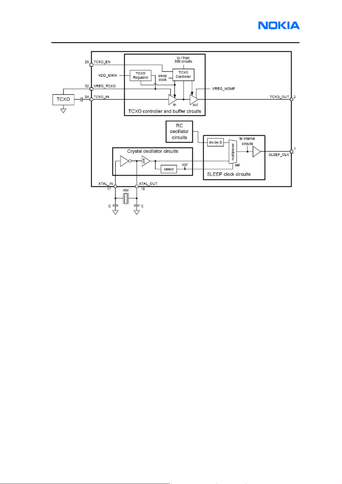
Figure 4: TCXO & SLEEP_XTAL Block Diagram
TCXO
The MSM device integrates a phase-locked loop from the TCXO clock input.
The PM optimizes TCXO operation that enables and disables appropriate circuits in
the proper sequence. The controller is enabled by the TCXO_EN signal from the
MSM.
When the selected transition occurs at TCXO_EN, the controller quickly enables the
TCXO regulator and the input buffer, and begins counting SLEEP_CLK pulses.
Within the initial power on period, the TCXO will be stabilized to its own calibrated
frequency. This initial period, in units of 32.768 kHz clock pulses, is programmed into
a timer within the controller. When the timer expires, the output buffer is enabled. It
synchronizes with the TCXO input such that the TCXO_OUT (MSM_TCXO in
schematic) signal is glitch free, only valid TCXO pulses are output.
Page 12 © 2006 Nokia Corporation Company Confidential Issue 1 12/2006
Page 13
7088 (Flower)
Nokia Customer Care Baseband Description and Troubleshooting
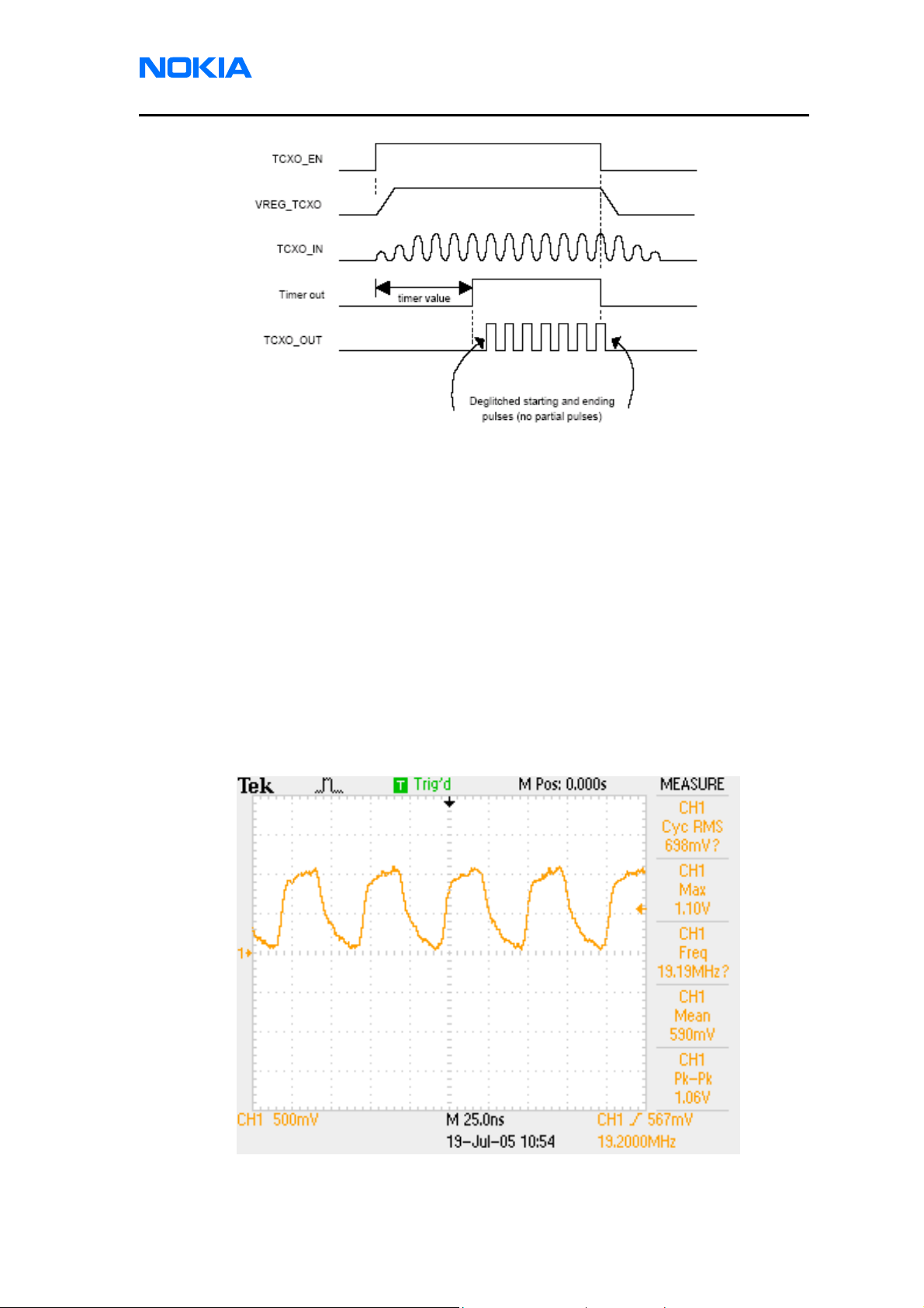
Figure 5: TCXO Enable Timing Diagram
The input buffer (TCXO_IN) accepts sinusoidal or square wave signals at or near
19.2 MHz. The input buffer (TCXO_IN) is powered from the TCXO regulator while
the output buffer is powered by VDD_MSMP.
The regulator of TCXO is turned off after the TCXO_EN signal is removed. Upon
power-up, the PM defaults to this SBI-controlled mode with the TCXO defaulted on.
This assures the MSM will always have a clock available immediately at power-up
even if TCXO_EN is low.
TCXO waveform (19.2MHz)
0
Figure 6: TCXO Timing at 25
Issue 1 12/2006 © 2006 Nokia Corporation Company Confidential Page 13
C
Page 14
7088 (Flower)
Base band Description and Troubleshooting
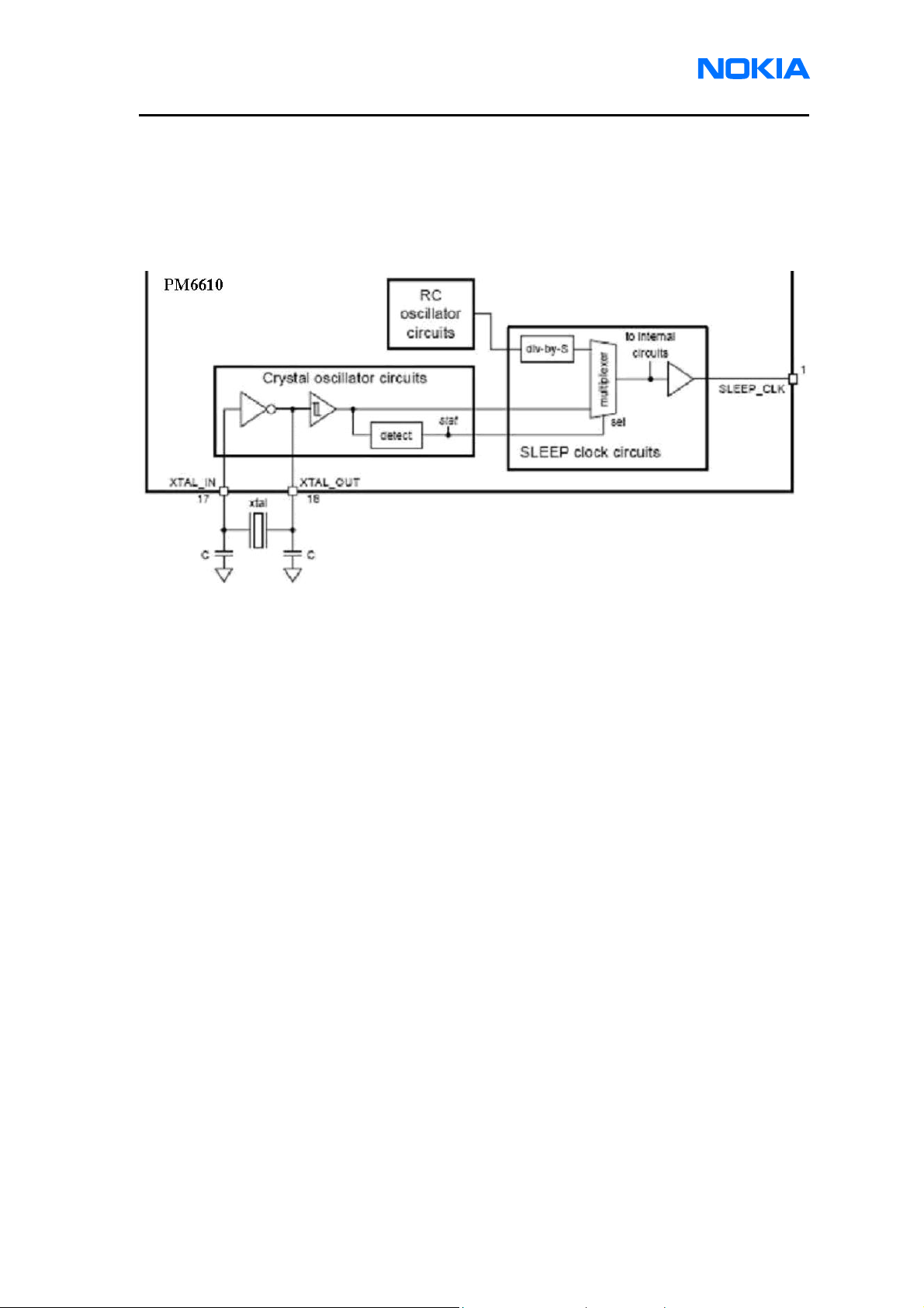
SLEEP crystal circuit for 32.768 kHz
The 32.768 kHz crystal oscillators is the primary SLEEP clock source when TCXO
clocks are disabled to save power.
Figure 7: Sleep CLK Block Diagram
The 32.768 kHz crystal oscillator signal is generated by an external crystal, which is
supplemented by a PM internal inverter and buffer.
The crystal oscillator continues to run as long as a valid supply is available, even
when the PMIC is powered down. This provides a continuous and accurate 32.768
kHz source. The oscillator halts when power from the external supply and main
battery are removed.
The PM includes a circuit that continually monitors the crystal oscillator signal. If the
crystal stops oscillating, the PM automatically switches to the RC oscillator and
sends an MSM interrupt. Narrow pulses at the SLEEP_CLK output may occur during
this switchover. The crystal oscillator dissipates little power, adjusting its bias current
to the minimum required to maintain oscillation.
SLEEP Clock waveform (32.768KHz)
Page 14 © 2006 Nokia Corporation Company Confidential Issue 1 12/2006
Page 15

7088 (Flower)
Nokia Customer Care Baseband Description and Troubleshooting
Figure 8: Sleep_CLK Timing at 250C
SBI CLK Interface
A 9.6 MHz clock signal is used for DBUS, which is used by the MSM to transfer data
between the PMIC and MSM6025.
Figure 9: MSM to PM SBI Timing at 250C
Issue 1 12/2006 © 2006 Nokia Corporation Company Confidential Page 15
Page 16

7088 (Flower)
Base band Description and Troubleshooting
The system clock is stopped during sleep mode by disabling the VREG_TCXO.
The PMIC regulator turns off the TCXO, which is from MSM’s TCXO_ON output
signal.
Backend IC and Camera Module Clocks
Figure 10: backend IC and camera module clocks
Backend IC (U11) uses external 13MHz crystal (Y210) and internal PLL to generate
internal clocks. Backend IC provides 24MHz clock to camera module. Camera
module uses the 24MHz clock to generate 12MHz pixel clock.
Flash Programming Error Description
This table describes the errors condition during Flash memory downloading to the
mobile terminal.
Description Not Working Properly
Packet Checksum fail ERR: CRC invalid
Erase fail Unable to erase device
Write fail Write unsuccessfully
Figure 11: Flash Programming Error Description
Page 16 © 2006 Nokia Corporation Company Confidential Issue 1 12/2006
Page 17

7088 (Flower)
Nokia Customer Care Baseband Description and Troubleshooting
Charging Operation
Battery
Flower uses a Lithium-Ion cell battery with a capacity of 700 mAh. Inside the
battery, there is a resistor connecting between BSI pin and GND pin for battery
ID, MSM reads the BSI pin (via VBATT_ID signal in schematic) to identify the
battery size. Different charging algorithms will be used for different battery sizes.
Figure 12: BL-4B battery pack pin order
Charging Circuitry
The PM6610 IC charge control is subject to the charger type and the battery size.
External components are needed for electromagnetic compatibility (EMC), and
transient protection of the input to the base band module. The charger’s DC input is
through the dc-jack connector. This mobile terminal supports AC-3, AC-4, DC-4,
AC-5, ACP-12 and AC-1 chargers.
Figure 12: Charging Circuitry
Issue 1 12/2006 © 2006 Nokia Corporation Company Confidential Page 17
Page 18

7088 (Flower)
Base band Description and Troubleshooting
Charger Detection
Connecting a charger creates a voltage on the VCHG (“VEXT_DC” net in schematic)
input of the PM6610. Charging starts when the PM6610 detects the VCHG input
voltage level above 3.3V (Min. working voltage of VCHG pin).
The VCHG signal of PM is generated to indicate the presence of the charger for the
software. The power management (PM) software controls the charger identification/
acceptance. The charger recognition is initiated when the EM software receives
a ”charger connected” interrupt. The algorithm basically consists of the following
three steps:
1. Check that the system current (the collector current of PNP transistor) is within
safety limits.
2. Check the power consumption of PNP transistor is within safety limits.
3. Check that the charger is within the charger window (voltage and current). If the
charger is accepted and identified, the appropriate charging algorithm will be
initiated.
Figure 13: Mobile terminal DC Jack power input circuit.
Figure 14: PNP Charging Control Circuit.
Page 18 © 2006 Nokia Corporation Company Confidential Issue 1 12/2006
Page 19

7088 (Flower)
Nokia Customer Care Baseband Description and Troubleshooting
Charge Control
In active mode, charging is controlled by the PM6610’s digital part. Charging voltage
and current monitoring are used to limit charging into a safe area. The PM6610 has a
MaxPower protection limit at PNP transistor to cut-off charger.
Cut Off MaxPower = 1W
The PM6610 limits the charging voltage to MaxVoltage.
MaxVoltage= 4.25V
The PM6610 limits the total system current (the collector current of PNP transistor)
by limiting the maximum power of PNP transistor charge.
Audio
The audio control and processing is provided by the MSM that contains the audio
codec, the MCU and DSP blocks. These blocks handle and process the audio data
signals. The baseband supports 2 microphone inputs and three receiver (earpiece)/
speaker outputs.
Figure 15: Audio Sending Direction Block Diagram
MIC+ & MIC- are used for the mobile terminal's internal microphone. JACK_MIC+ &
Issue 1 12/2006 © 2006 Nokia Corporation Company Confidential Page 19
Page 20

7088 (Flower)
Base band Description and Troubleshooting
JACK_MIC- are used for headsets.
The internal microphone (MIC+/-) is differential AC connection to the MSM
(MIC1P/N). The headset microphone is single-ended AC connection to the MSM
(MIC2P/N).
The MICBIAS output (“MIC_BIAS” signal) is used for internal microphone bias to
provide 0.2 mA of current at 1.8 Volts DC.
VDD_MSMP (2.95V) regulated voltage from PM IC is used for headset microphone
bias.
Figure 16: Audio Receiving Direction Block Diagram
RECEIVER+ & RECEIVER- (MSM pins EAR1OP & EAR1ON) differential outputs are
used for the mobile terminal's internal receiver. HPH_L (MSM pin EAR2)
single-ended output is used for accessory external headset. AUXOP & AUXON
differential outputs are used to drive external loudspeaker via external audio power
amplifier (U100).
The output power for the differential (EAR1O) output is typically 35 mW for a
full-scale +3 dBm0 sine wave into a 32 ohm receiver.
The output power for the single-ended (EAR2) output is typically 8.8 mW for a
full-scale +3 dBm0 sine wave into a 32 ohm receiver (earpiece).
The output power for the auxiliary (AUXO) output is typically 1.87 mW for a full-scale
+3 dBm0 sine wave into a 600 OHM load.
Page 20 © 2006 Nokia Corporation Company Confidential Issue 1 12/2006
Page 21

7088 (Flower)
Nokia Customer Care Baseband Description and Troubleshooting
Keypad
The mobile terminal uses six blue light-emitting diodes (LEDs) for keypad illumination.
MSM GPIO42 is used to turn on/off these LEDs.
MSM uses GPIO57 ~ GPIO66 (KYPD_0, KYPD_1, KYPD_3, ~ KYPD_17) to do
keypad scan function.
Display
Figure 17: LCD Module Block Diagram
The mobile terminal LCD is 128*160 dot matrix transmissive color TFT LCD.
The LCD module contains three serial white LEDs for LCD backlight. LEDs are
driven by a booster (U12). The enable/disable of booster is controlled by
BACKLIGHT_EN signal. BACKLIGHT_ADJ signal driven by MSM is used for
adjustment of LEDs luminance.
Issue 1 12/2006 © 2006 Nokia Corporation Company Confidential Page 21
Page 22

7088 (Flower)
Base band Description and Troubleshooting
Camera and Flash Light LED
Figure 18: Camera and Flash Light LED Block Diagram
The mobile terminal has a camera module. The camera module uses CMOS sensor
with 640*480 resolution and fixed focus lens. The camera module is connected to
backend IC (U11) via camera connector (J21).
Flash light LED is driven by booster (U240). The enable/disable of booster is
controlled by backend IC via FLASH_EN signal.
Universal Serial Bus (USB)
Figure 19: USB Block Diagram
The mobile terminal has a Universal Serial Bus (USB) interface for data access. The
USB interface supports full-speed (12 Mbps) transmission and receiving. It is compliant
with the Universal Serial Bus Specification Rev. 2.0.
Page 22 © 2006 Nokia Corporation Company Confidential Issue 1 12/2006
Page 23

7088 (Flower)
Nokia Customer Care Baseband Description and Troubleshooting
The following table lists the signals and their functions.
Signal Function
USB_VPO Differential output (+)
USB_VMO Differential output (–)
USB_RCV Single-ended input from USB transceiver; driven LOW when
input USB_SUSPEND is HIGH;
USB_OE_N An active low output used to enable or disable the D+ and D–
pins of the transceiver.
USB_READY Software controlled USB connection; allows USB connect or
disconnect signaling to be controlled by software
USB_SUSPEND Indicating suspending state
USB_INSERT_INT VBUS indicator;
“High”: When VBUS > 4.1 V, or USB_SUSPEND = HIGH
“Low”: When VBUS < 3.6 V
D+ Positive USB data bus connection (analog, differential)
D- Negative USB data bus connection (analog, differential)
VBUS USB bus power
Issue 1 12/2006 © 2006 Nokia Corporation Company Confidential Page 23
Page 24

7088 (Flower)
Base band Description and Troubleshooting
Accessories
The Flower supports the following accessories.
Figure 20: Pop-port bottom connector pin out
The pins out on the Flower connector are as follows:
• DC Charger Input Blue
• USB port Purple
• Headset Jack Green
You can perform the followings on Flower accessories:
• Charging
• Audio interface headset microphone and receiver (earpiece)
• Data access
Charging
This mobile terminal supports AC-3, AC-4, DC-4, AC-5, ACP-12 and AC-1 chargers,
and is connected through this interface.
Headset Detection
The mobile terminal supports Nokia standard 2.5mm mono headset. The headset
insertion to the mobile terminal is detected by pin 2 of the headset Jack, J701.
JACK_SENSE_N signal is low when headset not inserted. It becomes high when
headset is inserted.
Page 24 © 2006 Nokia Corporation Company Confidential Issue 1 12/2006
Page 25

7088 (Flower)
Nokia Customer Care Baseband Description and Troubleshooting
Figure 21: Headset Detection Circuit
Data Access
This mobile terminal has a USB port. Connect the USB port to a PC. Use the utility
program to access the data on mobile terminal.
UIM CARD
This mobile terminal supports UIM Card function. Figure 22 shows the timing of the
UIM’s serial interface.
UIM_DATA
UIM_CLK
UIM_REST
VREG_RUIM
Figure 22: UIM Card Serial Timing
Issue 1 12/2006 © 2006 Nokia Corporation Company Confidential Page 25
Page 26

7088 (Flower)
Base band Description and Troubleshooting
Test Points
Main Board Top Layer Test Points
Page 26 © 2006 Nokia Corporation Company Confidential Issue 1 12/2006
Page 27

7088 (Flower)
Nokia Customer Care Baseband Description and Troubleshooting
Main Board Bottom Layer Test Points
Issue 1 12/2006 © 2006 Nokia Corporation Company Confidential Page 27
Page 28

7088 (Flower)
Base band Description and Troubleshooting
Sub Board Top Layer Test Points
Page 28 © 2006 Nokia Corporation Company Confidential Issue 1 12/2006
Page 29

7088 (Flower)
Nokia Customer Care Baseband Description and Troubleshooting
Sub Board Bottom Layer Test Points
Issue 1 12/2006 © 2006 Nokia Corporation Company Confidential Page 29
Page 30

7088 (Flower)
Base band Description and Troubleshooting
Troubleshooting
First, carry out a thorough visual check of the module. Make sure in particular
that:
• There is no mechanical damage.
• Soldered joints are OK.
• ASIC orientations are OK.
The following hints should help find the cause of the problem when the
circuitry seems to be faulty. Troubleshooting instructions are divided into the
following sections:
• "Mobile Terminal is Dead"
• "Flash Memory Faults"
• "Power Does Not Stay ON or the Mobile Terminal is Jammed"
• "Charger Faults"
• "Audio Faults"
• "Display Faults"
• "Keypad Faults"
• "Camera Faults"
Note:
• MSM6025 (U625) is under filled and cannot be replaced.
• Memory IC (U6) is under filled and cannot be replaced.
• Backend IC (U11) is under filled and cannot be replaced.
• The Base band Shielding Cover Assy and RF Shielding Cover cannot
be reused after removal.
• After using the heat gun, the dome sheet is recommended to be
replaced.
Page 30 © 2006 Nokia Corporation Company Confidential Issue 1 12/2006
Page 31

7088 (Flower)
e
/
Nokia Customer Care Baseband Description and Troubleshooting
Mobile Terminal is Dead
Mobile
Terminal is
Dead
♦ If current is zero, check L101,Q400, R710, F1
and check the power on sequence. If there is
no powe r o u t pu t , reheat solder joints o r
change PM6610.
Is the mobile
terminal current is
zero or too high?
NO
YES
♦ Make sure all BB regulators are at their respectiv
voltage levels (VDD_MSMA, VDD_MSMP,
VDD_MSMC, VREG_TCXO). Reheat solder
joints / change PM6610 if necessary.
Is the current
< 60 mA?
YES
Check RESET_N
signals. Is it high
(2.8V)?
YES
Check PS_HOLD
signals. Is it high
(2.9V)?
NO
Check J101, C108, C109
NO
and R110.
Are they OK?
Reheat solder
NO
joints , check R836
or change PM6610
YES
Is flash memory
programming OK?
YES
YES
NO
Reheat solder joints
change PM6610.
MSM6025 is
defective, phone can
not be repaired and
must be replaced.
Flash
NO
Memory
Faults
Mobile
Terminal is
Jammed
Check LCM_OE_N
(same as OE_N). Is it
toggling after
RESET_N goes high?
NO
YES
Memory IC is
defective, phone can
not be repaired and
must be replaced.
MSM6025 is defective,
phone can not be repaired
and must be replaced.
© 2006 Nokia Corporation Company Confidential Page 31
Issue 1 12/20
06
Page 32

7088 (Flower)
Y
Y
Base band Description and Troubleshooting
Flash Memory Faults
Flash
Memory
Faults
Measure 19.2MHz
MSM_TCXO. Is it
YES
Can the mobile
terminal connect to
PC via USB?
YES
Check ROM_CS_N
and WE_N. Are they
toggling during
programming?
NO
NO
NO
Measure the
19.2MHz CLK
coming from the
ES
MSM6025 is defective,
phone can not be repaired
and must be replaced.
Memory IC is
defective, phone can
not be repaired and
must be replaced..
Is it work?
ES
END
MSM6025 is
defective, phone can
not be repaired and
must be replaced.
Check/ change
VREG_TCXO, Y102,
NO
R839, R849, C870,
C871, C868, C869,
R853 and C863
Mobile
NO
Terminal is
Jammed
YES
Memory IC is
defective, phone can
not be repaired and
must be replaced.
Page 32 © 2006 Nokia Corporation Company Confidential Issue 1 12/2006
Page 33

7088 (Flower)
Y
C
Y
r
Y
g
Nokia Customer Care Baseband Description and Troubleshooting
Power Does Not Stay ON or the Mobile Terminal is Jammed
Mobile
Terminal
Measure VDD_MSMP,
VDD_MSMC,
VDD_MSMA, and
VREG_TCXO voltages.
Are they OK?
YES
Measure 32.768kHz
Sleep CLK. Is it OK?
YES
Measure 19.2MHz
MSM_TCXO. Is it
Check VPH_PWR, VDD_MSMP,
VDD_MSMC, VDD_MSMA, and
NO
VREG_TCXO capacitors. Are
they OK?
YES
Check VBATT_ID
and
VPH_PWR. Are they
ES
NO
Measure the 32.768
ES
Reheat solder joints o
change PM6610
Measure the
NO
19.2MHz CLK
coming from the
ES
NO
NO
Reheat solder
joints or
PM6610
NO
hange Y1
Check/ reheat solder
joints/ change
NO
VREG_TCXO, Y102,
R839, R849, C870,
C871, C868 and
Repair capacitors, reheat
solder joints/ change
TCXO(Y102) and PM6610
change
C869.
YES
MSM6025 is
defective, phone can
not be repaired and
must be replaced.
Measure RESET_N.
Is it high (2.8V)?
YES
NO
Reheat solder joints
or chan
e PM6610
MSM6025 is
defective, phone can
not be repaired and
must be replaced.
Issue 1 12/2006 © 2006 Nokia Corporation Company Confidential Page 33
Page 34

7088 (Flower)
r
V
Base band Description and Troubleshooting
Charger Faults
Charge
Faults
Connect the charger
and make sure the
battery is
connected.
Check
BATT_ID. Is it
about 75k Ohm or 81k
Ohm in battery?
YES
Measure voltage at
VEXT_DC (TP161).
Is it >4.5V?
YES
Read MOBILE
TERMINAL_THERM
value. Is it room
temperature?
YES YES
Check/ change DC
NO
Jack, C108, C109,
R110 and
VDD_MSMA.
Check/ change DC Jack,
NO
F1, L101, D1006, D1007,
C1030, C874, R864 and
Q400.
Check NTC R4021and
NO NO
R300. Are they OK?
MSM6025 is defective,
phone can not be
repaired and must be
replaced.
Replace
NTCR4021,
R300
Measure voltage
between pin#1 and pin#3
of Q400. Is it >0.7V
YES
Change Q400
NO
Check R851.
Is it OK?
YES
Reheat solder joints or
change PM 6610
NO
Page 34 © 2006 Nokia Corporation Company Co
Reheat solder joints/
change R851
nfidential Issue 1 12/20
06
Page 35

7088 (Flower)
r
Nokia Customer Care Baseband Description and Troubleshooting
Audio Faults
Audio
Faults 1
Is the on-board
receiver working?
YES
NO
Replace the
receiver
(earpiece). Is it
working now?
NO
Use CCS Service
Software
Audio/Vibra
TestingStereo
Receiver Mobile
terminal Receiver Loop Back
Test command
Is the signal coming out of the
MSM6025
on RECEIVER+ and
RECEIVER- ?
YES
YES
Retest
Check/ change R511, R512,
C427, C426, C425, D421 and
D422 . Is it OK?
NO
YES
Audio
Faults
Page 2
MSM6025 is defective, phone
can not be repaired and must
be replaced.
Change the receive
Issue 1 12/2006 © 2006 Nokia Corporation Company Confidential Page 35
Page 36

7088 (Flower)
g
/
Base band Description and Troubleshooting
Audio
Faults 2
Is onboard
microphone
working?
YES
Replace the
NO
microphone. Is it
workin
now?
NO
Use CCS Software
Testing
Stereo Audio/Vibra
MicrophoneMobile terminal
Microphone Test command
Measure microphone bias voltage at
pin 1 of microphone. Is it 1.3V~ 1.5V?
YES
Is the signal going to the MSM6025
between MIC+ and MIC- ?
YES
YES
NO
NO
Retest
change R716,
Check
C701 and R717. If OK,
MSM6025 is
defective, phone can
not be repaired and
must be replaced.
Check/ change C713,
C706, C707, D410 and
D411. If OK,
MSM6025 is
defective, phone can
not be repaired and
must be replaced.
Audio
Retest
Faults
Page 3
Page 36 © 2006 Nokia Corporation Company Confidential Issue 1 12/2006
Page 37

7088 (Flower)
r
Nokia Customer Care Baseband Description and Troubleshooting
Audio
Faults 3
Is the internal
handsfree speaker
working?
YES
Audio
Faults
Page 4
Select a ring tone and
NO
measure signal between
J424 Pin1 and Pin2. Is the
signal OK?
NO
Measure AUDIO_EN
(AUDIO_ENABLE on main
board). Is it OK (2.9V)?
YES
Measure signal between
SPK_N and SPK_P . Is the
signal OK?
NO
Check/ change R173, C171,
C172,C174 and C175.R175~R1 78.
Check VPH_PWR. Are the signals
OK?
YES
Replace U100 and retest.
YES
NO
Yes
Change speake
MSM6025 is
defective, phone
can not be repaired
and must be
replaced.
Check/changeL815,
L816,C509,C510,C5
11,C512.
Issue 1 12/2006 © 2006 Nokia Corporation Company Confidential Page 37
Page 38

7088 (Flower)
r
Base band Description and Troubleshooting
Audio
Faults 4
Use CCS
Is the vibrator
working?
YES
NO
Software
Audio/Vibra
Control Test Command
Measure the VIB_DRV signal
on the vibrator. Is the signal
OK?
Testing Stereo
Vibrator
YES
NO
Check CR01
and C25. Are
they OK?
YES
NO
Change and
retest
END
Change the vibrato
Change PM 6610
Page 38 © 2006 Nokia Corporation Company Confidential Issue 1 12/2006
Page 39

7088 (Flower)
at
Nokia Customer Care Baseband Description and Troubleshooting
Display Faults
Display
Faults
Do the backlight
LEDs turned on
when the mobile
terminal is turned
on or when making
a call?
YES
NO
Check voltage across
L122_pin1 > 9V. Is it OK?
No
Measure battery voltage
D121 pin1. Is it OK?
YES
Check/change D121,
L123,and R127. Is each
one OK?
YES
Measure BACKLIGHT_EN
at U12_pin4. Is it high?
YES
Yes
NO
NO
NO
Check R126. If OK,
replace LCD Module
Check/ change
battery, VPH_PWR
and check FPC
connection.
Replace the
component and
retest
Check C233. If OK,
MSM6025 is defective,
phone can not be repaired
and must be replaced.
Check U12_pin1. Does it
switch between 0V and
YES
Check BACKLIGHT_ADJ
< 0.263 V. Is it OK?
NO
NO
Replace U12 and
retest.
Check D417
Display
YES
Faults 2
Replace U12 and retest
Issue 1 12/2006 © 2006 Nokia Corporation Company Confidential Page 39
Page 40

7088 (Flower)
Base band Description and Troubleshooting
Display
Faults
Page2
Does LCD display
start?
YES
Display
Faults 3
NO NO
and D_VDD (1.88V). Is each
one OK?
Check power IO_VDD (2.95V)
YES
Check power
TFT_VDD_MSMP(2.95V),I s it
NO
ok?
YES
Check/change U20,U21,U22
and FPC connection
J31.Check LCD
NO
signals:TFT_MAIN_CS,TFT_R
S,TFT_WE and LCD_RST, are
they ok?
YES
Check/change FPC
connection(J41A) and
PM6610
Replace L411 and
retest
Backend IC is
defective. Phone
can not be repaired
and must be
replaced
LCD is defective. Replace
LCD Module board
Page 40 © 2006 Nokia Corporation Company Confidential Issue 1 12/2006
Page 41

7088 (Flower)
Nokia Customer Care Baseband Description and Troubleshooting
Keypad Faults
Keypad
Faults
Measure voltage at
PHONE_ON (TP221
on main board and
Is the power
key working?
NO NO
TP2221 on sub
board) (2.8V).
Check FPC
Connention. If OK,
change PM6610
YES
Keypad
Faults
Page 2
YES
Measure voltage at
PHONE_ON when
power key is pressed.
Is it Low?
NO
Replace
Keymat
YES
Retest
Issue 1 12/2006 © 2006 Nokia Corporation Company Confidential Page 41
Page 42

7088 (Flower)
p
Base band Description and Troubleshooting
Keypad
Faults
Page 2
Check/change D350 and
D351.Then retest.
YES
Measure KYPD_(0,1,3,5,7)
Are the keys
working?
YES
NO
signals between MSM6025
and keypad at every outer
dome key. Are they ~ 2.9V?
YES
Measure
KYPD_(9,11,13,15,17)
signals between
MSM6025 and keypad
on every inner dome
Key. Are they about
NO
NO
Make sure there are no shorts
on KYPD_(0,1,3,5,7)?
NO
MSM6025 is defective can
not be repaired and must be
replaced
NO
Make sure there are no shorts
on KYPD_(9,11,13,15,17)?
YES
END
YES
MSM6025 is defective,
phone can not be
repaired and must be
re
laced
Check/change D352~D354(on
main board), then retest.
Page 42 © 2006 Nokia Corporation Company Confidential Issue 1 12/2006
Page 43

7088 (Flower)
Nokia Customer Care Baseband Description and Troubleshooting
Camera Faults
Camera
Faults
Can the camera
preview?
NO
Unplug camera and
check camera
socket(J21)
connection, then
plug the camera.
Can the camera
preview?
No
Yes
Retest
Yes
Take a picture.
Does the picture is
blurred?
No
Yes
Check power
D_VDD (~1.88VV)
Is it OK?
YES
Check power
IO_VDD (~2.95V)
Is it OK?
YES
Check power
A_VDD (~2.7V)
Is it OK?
YES
Check signals
CAM_RST,
CAM_PWDN,
CAM_XCLK,
CAM_SDATA and
CAM_SCK. Are the
signals OK?
NO
NO
NO
NO
Check/ change
L413
Check/ change
L411
Check/ change
U23,C221,
C222,C224 and
R226. And check
VPH_PWR
Backend IC is
defective. Phone
can not be repaired
and must be
replaced.
YES
END
Replace camera
module and retest.
Issue 1 12/2006 © 2006 Nokia Corporation Company Confidential Page 43
Page 44

7088 (Flower)
Base band Description and Troubleshooting
This page intentionally left blank.
Page 44 © 2006 Nokia Corporation Company Confidential Issue 1 12/2006
 Loading...