

Page 1

CCS Technical Documentation
NSB-9 Series Transceivers
System Module and User
Interface
Issue 1 04/03 Nokia Corporation
Page 2

NSB-9
System Module and User Interface CCS Technical Documentation
Table of Contents
Page No
Glossary of terms ........................................................................................................... 3
Introduction.................................................................................................................... 6
System Module: Baseband............................................................................................. 7
Baseband Module, technical summary ........................................................................7
Baseband Technical Specifications .............................................................................9
Absolute Maximum Ratings...................................................................................... 9
DC Characteristics..................................................................................................... 9
Power Distribution diagram .................................................................................... 11
Baseband External and Internal Signals and Connections ........................................12
Internal Signals and Connections............................................................................ 12
External Signals and Connections........................................................................... 18
Baseband Functional Description ................................................................................ 23
Modes of Operation ...................................................................................................23
No supply ................................................................................................................ 23
Backup..................................................................................................................... 23
Acting Dead............................................................................................................. 23
Active ...................................................................................................................... 23
Sleep mode .............................................................................................................. 24
Charging .................................................................................................................. 24
Power Up and Reset ...................................................................................................24
Power up with PWR key ......................................................................................... 25
Power up when charger is connected ...................................................................... 25
Power up when battery is connected ....................................................................... 26
RTC alarm power up ............................................................................................... 27
A/D Channels .............................................................................................................27
FM Radio ...................................................................................................................28
FM-radio audio connections.................................................................................... 29
Keyboards ..................................................................................................................29
Engine Keyboard..................................................................................................... 29
Flip .......................................................................................................................... 30
Flip keyboard........................................................................................................... 30
Flip position detection............................................................................................. 31
IR Module ..................................................................................................................31
SIM Interface .............................................................................................................31
System Connector ......................................................................................................33
External accessory regulator ......................................................................................33
Battery ........................................................................................................................34
Backup Battery ..........................................................................................................35
LCD & Keypad Illumination .....................................................................................36
LCD ...........................................................................................................................37
ACI ............................................................................................................................38
External Audio ...........................................................................................................38
External Microphone Connection ........................................................................... 38
External Earphone Connections .............................................................................. 40
Internal Audio ............................................................................................................40
Internal Microphone................................................................................................ 40
Page 2 Nokia Corporation Issue 1 04/03
Page 3

NSB-9
CCS Technical Documentation System Module and User Interface
Internal Speaker....................................................................................................... 41
Integrated Hands Free ............................................................................................. 41
Memory Block ...........................................................................................................42
Security ......................................................................................................................42
Production / After Sales Interface ..............................................................................43
Issue 1 04/03 Nokia Corporation Page 3
Page 4

NSB-9
System Module and User Interface CCS Technical Documentation
Glossary of terms
ACI Accessory Control Interface
ADC Analog-Digital Converter
AEC Acoustic Echo Canceller
AFC Automatic Frequency Control
AGC Automatic Gain Control
AIF Application Interface
ALWE Background noise suppressor
AMS After Market Service
AMR Adaptive Multi Rate
ARM Processor architecture
ASIC Application Specific Integrated Circuit
BB Baseband
CBus Control Bus
CCS Customer Care Solutions
CMT Cellular Mobile Telephone (MCU and DSP)
CPU Central Processing Unit
CTSI Clocking Timing Sleep Interrupt
COG Chip On Glass
CSP Chip Scale Package
CSTN Color Super Twisted Nematic
DAC Digital-Analog Converter
DAI Digital Audio Interface
DB Dual band
Page 4 Nokia Corporation Issue 1 04/03
Page 5

NSB-9
CCS Technical Documentation System Module and User Interface
DCN Offset Cancellation control signal
DLL Dynamic Link Library
DRC Dynamic Range Controller
DSP Digital Signal Processor
EFR Enhanced Full Rate
EMC Electromagnetic compatibility
EMI Electromagnetic Interference
ESD Electro Static Discharge
EXT RF External RF
FBUS Asynchronous Full Duplex Serial Bus
GPRS General Packet Radio Service
GSM Global System for Mobile communications
HS Half Rate Speech
HSCSD High Speed Circuit Switched Data
IC Integrated Circuit
IHF Integrated Hands Free
I/O Input/Output
IrDA Infrared Association
LCD Liquid Crystal Display
LDO Low Drop-Out
LNA Low Noise Amplifier
MBUS 1-wire half duplex serial bus
MCU Micro Controller Unit
MDI MCU-DSP Interface
Issue 1 04/03 Nokia Corporation Page 5
Page 6

NSB-9
System Module and User Interface CCS Technical Documentation
MFI Modulator and Filter Interface
PA Transmit Power Amplifier
PC Personal Computer
PCM Pulse Code Modulation
PCM SIO Synchronous serial bus for PCM audio transferring
PIFA Planar Inverted F-antenna
PWB Printed Wiring Board
RF Radio Frequency
SIM Subscriber Identity Module
UEM Universal Energy Management
UI User Interface
UPP Universal Phone Processor
VCXO Voltage Controlled Crystal Oscillator
VCTCXO Voltage Controlled Temperature Compensated Crystal Oscillator.
Page 6 Nokia Corporation Issue 1 04/03
Page 7

NSB-9
CCS Technical Documentation System Module and User Interface
Introduction
The system module RM9 consists of Radio Frequency (RF) and baseband (BB). User Interface (UI) contains display, keyboard, IR link, vibra, HF/HS connector and audio parts. Part
of the keyboard is implemented in separate flip module, named TF9.
FM radio is located on the main PWB RM9. Headset is used as an antenna for FM radio.
The electrical part of the T9 and half of qwerty keyboard is located inside Flip. TF9 is connected to radio PWB through four 2-pole poco connectors
NSB-9 has Pop-Port accessory interface. Both two and three wire type of chargers are
supported. BLC-2 Li-ion battery with nominal capacity of 1000 mAh is used as main
power source.
The Baseband blocks provide the MCU, DSP, external memory interface and digital control functions in the UPP ASIC. Power supply circuitry, charging, audio processing and RF
control hard ware are in the UEM ASIC.
The purpose of the RF block is to receive and demodulate the radio frequency signal from
the base station and to transmit a modulated RF signal to the base station.
Issue 1 04/03 Nokia Corporation Page 7
Page 8

NSB-9
System Module and User Interface CCS Technical Documentation
System Module: Baseband
Baseband Module, technical summary
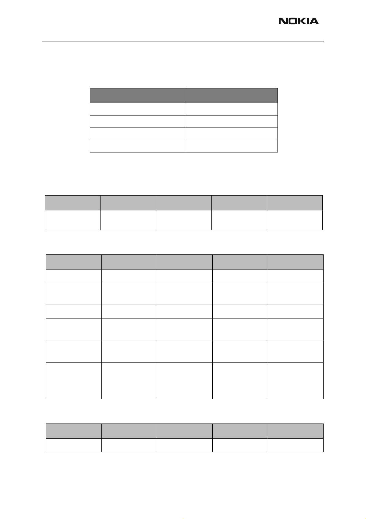
Main functionality of the NSB-9 baseband is implemented with two ASICs: UPP (Universal Phone Processor) and UEM (Universal Energy Management).
Figure 1: Baseband Block Diagram
RF interface
RF interface
(GSM)
(GSM)
IR
LCD
LCD
LED driver
LED driver
VIBRA
VIBRA
IR
Memories
Memories
128M FLASH
128M FLASH
(incl. EEPROM)
(incl. EEPROM)
8M SRAM
8M SRAM
HALL sw.
HALL sw.
SIM
SIM
Battery
Battery
BLC-2
BLC-2
VOUT
VOUT
2.8V
2.8V
Charger
Charger
Baseband is running from power rails 2.8V analog voltage and 1.8V I/O voltage. UPP core
voltages can be lowered down to 1.0V, 1.3V and 1.5V. UEM includes 6 linear LDO (low
drop-out) regulators for baseband and 7 regulators for RF. It also includes 4 current
sources for biasing purposes and internal usage. UEM also includes SIM interface which
has supports both 1.8V and 3V SIM cards.
UEMK UPP8M
UEMK UPP8M
Mo/St Amp
Mo/St Amp
LM4855
LM4855
DC
DC
DC
jack
jack
jack
System connector
System connector
System connector
Tomahawk
Tomahawk
Tomahawk
KEYBOARD
KEYBOARD
KEYBOARD
KEYBOARD
1.8V
1.8V
L
L
FM radio
FM radio
R
R
ENGINE
ENGINE
FLIP
FLIP
uC
uC
A real time clock function is integrated into the UEM which utilizes the same 32kHz
clock supply as the sleep clock. A backup power supply is provided for the RTC which
keeps the real time clock running when the main battery is removed. The backup power
supply is a rechargeable surface mounted battery (capacitor type). The backup time with
the battery is 30 minutes minimum.
The analog interface between the baseband and the RF section is handled by a UEM
ASIC. UEM provides A/D and D/A conversion of the in-phase and quadrature receive and
transmit signal paths and also A/D and D/A conversions of received and transmitted
Page 8 Nokia Corporation Issue 1 04/03
Page 9

NSB-9
CCS Technical Documentation System Module and User Interface
audio signals to and from the user interface. The UEM supplies the analog TXC and AFC
signals to RF section according to the UPP DSP digital control. Data transmission
between the UEM and the UPP is implemented using two serial busses, DBUS for DSP and
CBUS for MCU. RF ASIC, Hagar, is controlled through UPP RFBUS serial interface. There is
also separate signals for PDM coded audio. Digital speech processing is handled by the
DSP inside UPP ASIC. UEM is a dual voltage circuit, the digital parts are running from the
baseband supply 1.8V and the analog parts are running from the analog supply 2.78V
also VBAT is directly used by flip, stereo amplifier, IR and some other blocks.
The baseband supports both internal and external microphone inputs and speaker outputs. UEM also includes third microphone input which is used in NSB-9 for FM radio
with IHF use (Left channel). Input and output signal source selection and gain control is
done by the UEM according to control messages from the UPP. Keypad tones, DTMF, and
other audio tones are generated and encoded by the UPP and transmitted to the UEM for
decoding. An external vibra alert control signal is generated by the UEM with separate
PWM outputs.
NSB-9 has two external serial control interfaces: FBUS and MBUS. These busses can be
accessed only through production test pattern.
EMC shielding for baseband is implemented using a metal shielding can. Although some
components are outside the shielding can. On the other side the engine is shielded with
PWB grounding. Heat generated by the circuitry will be conducted out via the PWB
ground planes.
Full functionality according to the specifications needs to be met through ambient temperature range -10 °C to +55 °C. Storage temperature range -40 °C to +85 °C.
Issue 1 04/03 Nokia Corporation Page 9
Page 10
NSB-9
System Module and User Interface CCS Technical Documentation
Baseband Technical Specifications
Absolute Maximum Ratings
Table 1: Absolute Maximum Ratings
Signal Note
Battery Voltage (Idle) -0.3V - 5.5V
Battery Voltage (Call) Max 4.8V
Charger Input Voltage -0.3V - 16V
Charging current 850mA
DC Characteristics
Regulators and Supply Voltage Ranges
Table 2: Battery Voltage Range
Signal Min Nom Max Note
VBAT 3.1V 3.6V 4.2V (charging high
3.2V SW cut off
limit voltage)
Table 3: Baseband Regulators
Signal Min Nom Max Note
VANA 2.70V 2.78V 2.86V I
VFLASH1 2.70V
2.61V (Sleep)
2.78V 2.86V
2.95V (Sleep)
VFLASH2 2.70V 2.78V 2.86V I
VSIM 1.745V
2.91V
1.8V
3.0V
1.855V
3.09V
VIO 1.72V 1.8V 1.88V I
VCORE 1.0V
1.235V
1.425V
1.710V
1.053V
1.3V
1.5V
1.8V
1.106V
1.365V
1.575V
1.890V
max
I
max
I
sleep
max
I
max
I
sleep
max
I
sleep
I
max
I
sleep
Default value 1.5V
= 80mA
= 70mA
= 1.5mA
= 40mA
= 25mA
= 0.5mA
= 150mA
= 0.5mA
= 200mA
= 0.2mA
Table 4: Accessory Regulator
Signal Min Nom Max Note
Vout 2.72V 2.80V 2.88V I
max
= 80mA
Page 10 Nokia Corporation Issue 1 04/03
Page 11

NSB-9
CCS Technical Documentation System Module and User Interface
Table 5: RF Regulators
Signal Min Nom Max Note
VR1A 4.6V 4.75V 4.9V I
VR2 2.70V
2.61V (Sleep)
2.78V 2.86V
2.95V (Sleep)
VR3 2.70V 2.78V 2.86V I
VR4 2.70V 2.78V 2.86V I
VR5 2.70V 2.78V 2.86V I
VR6 2.70V 2.78V 2.86V I
VR7 2.70V 2.78V 2.86V I
max
I
max
max
max
I
sleep
max
I
sleep
max
I
sleep
max
= 10mA
= 100mA
= 20mA
= 50mA
= 0.1mA
= 50mA
= 0.1mA
= 50mA
= 0.1mA
= 45mA
Issue 1 04/03 Nokia Corporation Page 11
Page 12
NSB-9
System Module and User Interface CCS Technical Documentation
Power Distribution diagram
Figure 2: Baseband Power Distribution Diagram
Baseband
UEM
RF Regulators
VLED+
LCD LED
Driver
Battery CHACON
Flip
VBAT
VBAT
Audio
Amplifier
RTC
Accessory
Regulator
Baseband
Regulators
VR1A
VR1B
VR2-7
VSIM
VCORE
VANA
VIO
VFLASH1
VFLASH2
6
SIM
UPP
FLASH
LCD
Backup
battery
FM
Radio
PA Supply
Vout
Bottom Connector
VBAT
IRDA
Page 12 Nokia Corporation Issue 1 04/03
Page 13

NSB-9
CCS Technical Documentation System Module and User Interface
Baseband External and Internal Signals and Connections
This section describes the external and internal electrical connection and interface levels
on the baseband. Electrical interface specifications are collected into tables that covers a
connector or a defined interface.
Internal Signals and Connections
Table 6: FM Radio Interface
BB Signal
VFLASH2 VCC 2.7V 2.78 V 2.86V Analog supply voltage
GenIO(3) FMClk 1.4V
GenIO(8) FMWrEn 1.4V
GenIO(11) FMCtrlClk 1.4V
FM Radio
Signal
VDIG 2.7V 2.78V 2.86V Digital supply voltage
Min Nom Max Condition Note
6.0mA 8.4mA 10.5mA Operational
3uA 6uA Stand by
2.1mA 3.0mA 3.9mA Operational
11 uA 19uA 26uA Stand by
(bus enable
LOW)
0
0V
0
1.8V 1.88V
0.4V
32kHz Frequency
1.8V 1.88V
0.4V
1.8V 1.88V
0.4V
High
Low
High
Low
High
Low
Reference clock for
FM radio module
Also 6.5MHz or
13MHz can be used
Write Enable
max. 1MHz
GenIO(12) FMCtrlDa 1.4V
0
FMANT f
FM_RADIO R VAFR 720mV 850mV 940mV fRF=98MHz,
FM_RADIO L VAFL 720mV 850mV 940mV fRF=98MHz,
FM(ant)
76MHz 108MHz FM input frequency.
1.8V 1.88V
0.4V
High
Low
V
RF
V
RF
=1mV
=1mV
Bidirectional
Headset used as an
antenna.
FM-radio output signal (right) to amplifier
input
FM-radio output signal (left) to amplifier
input
Issue 1 04/03 Nokia Corporation Page 13
Page 14
NSB-9
System Module and User Interface CCS Technical Documentation
Table 7: AC and DC Characteristics of RF-Baseband Voltage Supplies
Signal
name
VBAT Battery PA, UEM,
VR1A UEM VCP Voltage 4.6 4.75 4.9 V Supply for varactor for
VR2 UEM VRF_TX Voltage 2.70 2.78 2.86 V Supply for part of
VR3 UEM VCTCXO Voltage 2.70 2.78 2.86 V Supply for VCTCXO
From To Parameter Min Typ Max Unit Function
Voltage 2.95 3.6 4.2 V Battery supply.
STEREO
AMPLIFIER, FLIP
Current 3 A
Current drawn
by PA when
”off”
Current 2 10 mA
Current 65 100 mA
Current 1 20 mA
0.8 2 uA
UHF VCO tuning.
transmit strip. Supply
for TX I/Q-modulators.
VR4 UEM VRF_RX Voltage 2.70 2.78 2.86 V Supply for Hagar RX;
preamp., mixer,DTOS
Noise density decades
20dB/dec from 6Hz to
600Hz. From f >600Hz
maximum noise density 55nV
Current 50 mA
VR5 UEM VDIG,
VPRE,
VLO
VR6 UEM VBB Voltage 2.70 2.78 2.86 V Supply for Hagar BB
VR7 UEM UHF VCO Voltage 2.70 2.78 2.86 V Supply for UHF VCO
Voltage 2.70 2.78 2.86 V Supply for Hagar PLL;
dividers, LO-buffers,
prescaler.
Current 50 mA
and LNA
Current 50 mA
Current 30 mA
RMS
/ÖHz.
Page 14 Nokia Corporation Issue 1 04/03
Page 15

NSB-9
CCS Technical Documentation System Module and User Interface
VrefRF01UEM VREF_RX Voltage 1.3341.35 1.366V Voltage Reference for
RF-IC.
Note:Below 600Hz
noise density is
allowed to increase 20
dB/oct
Current 100 uA
VrefRF02UEM VB_EXT Voltage 1.3231.35 1.377V Supply for RF-BB dig-
ital interface and
some digital parts of
RF.
Current 100 uA
Table 8: AC and DC Characteristics of RF-Baseband Digital Signals
Signal name From To Parameter Input Characteristics Function
TXP
(RFGenOut3)
RFBusEna1X UPP HAGAR ”1”
UPP
PA &
HAGAR
”1”
”0” 0 0.4 V
Load Resistance 10 220 kohm
Load
Capacitance
Timing Accuracy 1/4
”0” 0 0.4 V
Current 50 uA
Load resistance 10 220 kohm
Min Typ Max Unit
1.3
8
1.3
8
1.88 V
20 pF
symb
ol
1.88 V RFbus enable
Transmitter
power amplifier
enable / DCN2
timing???
Load capacitance 20 pF
RFBusData UPP HAGAR ”1” 1.38 1.88 V RFbus data;
read/write
”0” 0 0.4 V
Load resistance 10 220 kohm
Load capacitance 20 pF
Issue 1 04/03 Nokia Corporation Page 15
Page 16

NSB-9
System Module and User Interface CCS Technical Documentation
Data frequency 10 MHz
RFBusClk UPP HAGAR ”1” 1.38 1.88 V RFbus clock
”0” 0 0.4 V
Load resistance 10 220 kohm
Load capacitance 20 pF
Data frequency 10 MHz
RESET
(GenI/O6)
UPP HAGAR ”1” 1.38 1.85 V Reset to Hagar
”0” 0 0.4 V
Load capacitance 20 pF
Load resistance 10 220 kohm
Timing accuracy 1/4 sym-
bol
Page 16 Nokia Corporation Issue 1 04/03
Page 17

NSB-9
CCS Technical Documentation System Module and User Interface
Table 9: AC and DC Characteristics of RF-Baseband Analogue Signals
Signal name From To Parameter Min Typ Max Unit Function
High stability
clock signal for
the logic circuits,
AC coupled.
Distorted
sinewave eg.
sawtooth.
VCTCXO
VCTCX
O
UPP Frequency 13 26 MHz
Signal
amplitude
Input
Impedance
Input
Capacitance
Duty Cycle 40 60 %
VCTCXOGnd VCTXO UPP DC Level 0 V Ground for refer-
RXI/RXQ HAGAR UEM Differential volt-
age swing
(static)
DC level 1.3 1.35 1.4 V
TXIP / TXIN UEM HAGAR Differential volt-
age swing
(static)
0.2 0.8 2.0 Vpp
10 kohm
10 pF
ence clock
1.35 1.4 1.45 Vpp RX baseband signal.
2.23 2.48 Vpp Programmable
voltage swing.
Programmable
common mode
voltage.
Between TXIP-TXIN
DC level 1.17 1.20 1.23 V
Source Impedance
TXQP / TXQN UEM HAGAR Same spec as for TXIP / TXIN Differential quad-
AFC UEM VCTCXO Voltage Min
Max
Resolution 11 bits
Load resistance
and capacitance
0.0
2.4
1
200 ohm
0.1
2.6
100
V Automatic fre-
kohm
nF
rature phase TX
baseband signal for
the RF modulator
quency control signal for
VCTCXO
Issue 1 04/03 Nokia Corporation Page 17
Page 18

NSB-9
System Module and User Interface CCS Technical Documentation
Step settling
time
Aux_DAC
(TxC)
RFTemp RF UEM
Vbase RF UEM Voltage 2.7 V Detected voltage
UPP Pin Signal Min Nom Max Condition Note
UEM RF Voltage Min
Max
Source Impedance
Resolution 10 bits
Voltage at -20oC
Voltage at
o
+25
C
Voltage at +60oC
Table 10: Engine keyboard interface
2.4
1,57 V Temperature sensor
1,7
1,79
0.2 ms
0.1 V Transmitter power
control
200 ohm
of RF.
from PA power
level sensing unit
P00 COL(0) 0.7xVIO01.8V VIO
0.3xVIO
P01 COL(1) 0.7xVIO01.8V VIO
0.3xVIO
P02 COL(2) 0.7xVIO01.8V VIO
0.3xVIO
P03 COL(3) 0.7xVIO01.8V VIO
0.3xVIO
P04 COL(4) 0.7xVIO01.8V VIO
0.3xVIO
P05 /
GenI/O2
P10 ROW(0) 0.7xVIO01.8V VIO
P11 ROW(1) 0.7xVIO01.8V VIO
P12 ROW(2) 0.7xVIO01.8V VIO
P13 ROW(3) 0.7xVIO01.8V VIO
COL(5) 0.7xVIO01.8V VIO
0.3xVIO
0.3xVIO
0.3xVIO
0.3xVIO
0.3xVIO
High
Low
High
Low
High
Low
High
Low
High
Low
High
Low
High
Low
High
Low
High
Low
High
Low
Keyboard matrix column
0
Keyboard matrix column
1
Keyboard matrix column
2
Keyboard matrix column
3
Keyboard matrix column
4
Keyboard matrix column
5
Keyboard matrix row 0
Keyboard matrix row 1
Keyboard matrix row 2
Keyboard matrix row 3
P14 ROW(4) 0.7xVIO01.8V VIO
0.3xVIO
High
Low
Keyboard matrix row 4
Page 18 Nokia Corporation Issue 1 04/03
Page 19

NSB-9
CCS Technical Documentation System Module and User Interface
P15 ROW(5) 0.7xVIO01.8V VIO
0.3xVIO
GenI/O19 Shift 0.7xVIO01.8V VIO
0.3xVIO
Table 11: Stereo ampilifer interface
Stereo
BB signal
VBAT Vcc 3.1V 3.6V 4.2V Supply voltage
GND GND 0V Ground
GenI/O14 ENB 1.4V
GenI/O15 CLK 1.4V
amplifier
signal
Min Nom Max Condition Note
7.5mA 10mA Output
0.5uA Standby
1.8V 1.88V
0V
1.8V 1.88V
0V
0.4V
0.4V
High
Low
High
Low
mode 7,
Vin=0V,
Io=0A
High
Low
High
Low
Keyboard matrix row 5
Engine shift key
Chip enable, active
high
Clock input
GenI/O16 DATA 1.4V
0V
FM-RADIO L,
FM-RADIO R
XEAR Phone InHS,
Lin, Rin GND Vcc Lin, Rin input voltage
GND Vcc Phone in input volt-
Phone InIHF
1.8V 1.88V
0.4V
High
Low
External Signals and Connections
Table 12: Flip Connectors
Pin / Ref Signal Min Nom Max Condition Note
J301
J302
J303,
J304
J305,
J306
VBAT 3.1V 3.6 V 4.2V Flip Closed Flip supply voltage
2.9V 3.4V 4.0V Flip Open,
(load
switch)
DATA 0.7xVIO
0
CLOCK 0.7xVIO
0
0.3xVIO
0.3xVIO
High
Low
High
Low
Serial data input
age
GenI/O17
GenI/O18
J307,
J308
GND 0V Ground
Issue 1 04/03 Nokia Corporation Page 19
Page 20

NSB-9
System Module and User Interface CCS Technical Documentation
Table 13: LCD Connector (X300)
Pin Signal Min Nom Max Condition Note
1 VDD (VFLASH1) 2.72V 2.78V 2.86V Voltage supply
Connected to VFLASH1
2 XRES 0.8xVIO
0
1000ns t
3 SI 0.8xVIO
0
100ns t
100ns t
VIO
0.22xVIO
VIO
0.22xVIO
Logic ’1’
Logic ’0’
rw
Logic ’1’
Logic ’0’
sds
sdh
Reset
Active low
Reset active
Serial data (driver
input)
Data setup time
Data hold time
4 VDDI (VIO) 1.72V 1.8V 1.88V Logic voltage supply
Connected to VIO
5 XCS 0.8xVIO
0
130ns t
VIO
0.22xVIO
Logic ’1’
Logic ’0’
css
Chip select
Active low
XCS low before SCLK
rising edge
130ns t
csh
XCS low after SCLK rising edge
300ns t
csw
XCS high pulse width
6 SCLK 0.8xVIO
0
250ns t
11 0n s t
11 0n s t
VIO
0.22xVIO
6.5MHz
Logic ’1’
Logic ’0’
Max frequency
scyc
shw
slw
Serial clock input
Clock cycle
Clock high
Clock low
7 GND 0V Ground
8 LED -
0.505V
0V
0.525V
0.545V
LEDs OFF
LEDs ON
9 NC Not connected
10 LED +
9.505V
(9V+LED-)
0V
11.325V
(10.8V+LED)
12.545V
(12V+LED)
LEDs OFF
LEDs ON
Supply voltage for LCD
LEDs
Page 20 Nokia Corporation Issue 1 04/03
Page 21

NSB-9
CCS Technical Documentation System Module and User Interface
Table 14: DC Connector (X101)
Pin Signal Min Nom Max Condition Note
1 VCHAR 11 .1 V
7.0 V
RMS
8.4 V
RMS
peak
16.9
V
peak
7.9 V
RMS
1.0 A
peak
9.2 V
RMS
850 mA
Standard
charger
Fast
charger
Charger positive input
2 CHGND 0 Charger ground
Table 15: System Connector (X102)
Pin Signal
1 CHARGE Charge
2 GND Charge
DescriptionSpectral
range
DC 0...9V
Voltage
GND
UI levels Impedance Note
0.85A
100mΩ
(PWB + connector)
3 ACI Accessory
Control
1 kbit/s 0V
2.78V
47Ω Insertion & removal /
Control
Interface
4 VOUT DC out DC 2.78V
70mA
100mΩ
(PWB + connector)
5 Not connected in NSB-
9
6 FBUS RX 115 k bi t/ s 0...0.86V
33Ω
(logic ”0”)
2.0...3.0V
(logic ”1”)
7 FBUS TX 115 kb i t/ s 0...0.81V
33Ω
(logic ”0”)
1.89...2.83
V (logic
”1”)
8 Not connected in NSB-
9
9 XMIC N External
300...8k
mic input
10 XMIC P External
300...8k 2.1V DC
mic input
11 HSEAR N Ext audio
output
20...20k 10Ω Differential left channel
output
(left)
Issue 1 04/03 Nokia Corporation Page 21
Page 22

NSB-9
System Module and User Interface CCS Technical Documentation
12 HSEAR P Ext audio
ouput
(left)
13 HSEAR R N Ext audio
output
(right)
14 HSEAR R P Ext audio
output
(right)
Pin Name Parameter Min Typ Max Unit Notes
1 VSIM 1.8V SIM Card 1.6 1.8 1.9 V Supply voltage
3V SIM Card 2.8 3.0 3.2
2 SIMRST 1.8V SIM Card 0.9xVSIM
3V SIM Card 0.9xVSIM
20...20k 10Ω
20...20k 10Ω Differential right channel output
20...20k 10Ω
Table 16: SIM Connector (X386)
VSIM
0
0
0.15xVSIM
VSIM
0.15xVSIM
V SIM reset (output)
3 SIMCLK Frequency 3.25 MHz SIM clock
Trise/Tfall 50 ns
1.8V Voh
1.8V Vol
3 Voh
3 Vol
4 DATA 1.8V Voh
1.8V Vol
3 Voh
3 Vol
1.8V Vih
1.8V Vil
3V Vil
3V Vil
5 NC Not Connected
6 GND GND 0 V Ground
0.9xVSIM
0
0.9xVSIM
0
0.9xVSIM
0
0.9xVSIM
0
0.7xVSIM
0
0.7xVSIM
0
VSIM V
VSIM
VSIM
0.15xVSIM
VSIM
0.15xVSIM
VSIM
0.15xVSIM
VSIM
0.15xVSIM
V SIM data (output)
SIM data (input)
Trise/Tfall max 1us
Page 22 Nokia Corporation Issue 1 04/03
Page 23

NSB-9
CCS Technical Documentation System Module and User Interface
Table 17: Internal Microphone
Signal Min Nom Max Condition Note
MICP 200mV
AC 2.2kΩ to MIC1B
pp
2.0 V 2.1 V 2.25 V DC
MICN 2.0V 2.1V 2.25V DC
Table 18: Internal Speaker
Signal Min Nom Max Condition Note
EARP
0.75V 0.8V
EARN
0.75V 0.8V
2.0 V
0.85V
2.0 V
0.85V
pp
AC
Differential output
DC
(V
diff
pp
AC
DC
Table 19: Integrated hands free speaker
Signal Min Nom Max Condition Note
IHFP
V V
V
pp
V
AC
DC
Differential output
Vbat 4.1V, 1kHz, 8Ω,
1% THD
(V
diff
= 4.0 Vpp)
= 2.4Vpp)
IHFN
V V
V
pp
V
AC
DC
Table 20: Internal vibra
Signal Min Nom Max Condition Note
VBAT 3.1V 3.6V 4.2V
VIBRA 1.0V 1.5V 2.3V DC Udc_motor
Issue 1 04/03 Nokia Corporation Page 23
Page 24

NSB-9
System Module and User Interface CCS Technical Documentation
Baseband Functional Description
Modes of Operation
NSB-9 baseband has six different functional modes:
• No supply
• Back-up
•Acting Dead
•Active
• Sleep
• Charging
No supply
In NO_SUPPLY mode the phone has no supply voltage. This mode is due to disconnection
of main battery and backup battery or low battery voltage level in both of the batteries.
Phone is exiting from NO_SUPPLY mode when sufficient battery voltage level is detected.
Battery voltage can rise either by connecting a new battery with VBAT > VMSTR+ or by
connecting charger and charging the battery above VMSTR+.
Backup
In BACKUP mode the backup battery has sufficient charge but the main battery can be
disconnected or empty (VBAT < VMSTR and VBACK > VBUCOFF).
VRTC regulator is disabled in BACKUP mode. VRTC output is supplied without regulation
from backup battery (VBACK). All the other regulators are disabled.
Acting Dead
If the phone is off when the charger is connected, the phone is powered on but enters a
state called ”Acting Dead”. To the user the phone acts as if it was switched off. A battery
charging alert is given and/or a battery charging indication on the display is shown to
acknowledge the user that the battery is being charged.
Active
In the active mode the phone is in normal operation, scanning for channels, listening to
a base station, transmitting and processing information. There are several sub-states in
the active mode depending on if the phone is in burst reception, burst transmission, if
DSP is working etc.
Page 24 Nokia Corporation Issue 1 04/03
Page 25

NSB-9
CCS Technical Documentation System Module and User Interface
One of the sub-state of the active mode is FM radio on state. In that case UEM audio
blocks, stereo amplifier and FM radio are powered on. FM radio circuitry is controlled by
the MCU and 32kHz reference clock is supplied by the UPP. VFLASH2 regulator is operating.
In active mode the RF regulators are controlled by SW writing into UEM’s registers
wanted settings: VR1A can be enabled or disabled. VR2 can be enabled or disabled and
its output voltage can be programmed to be 2.78V or 3.3V. VR4 - VR7 can be enabled or
disabled or forced into low quiescent current mode. VR3 is always enabled in active
mode.
Sleep mode
Sleep mode is entered when both MCU and DSP are in stand-by mode. Sleep is controlled
by both processors. When SLEEPX low signal is detected UEM enters SLEEP mode. VCORE,
VIO and VFLASH1 regulators are put into low quiescent current mode. All RF regulators
are disabled in SLEEP. When SLEEPX=1 is detected UEM enters ACTIVE mode and all
functions are activated.
The sleep mode is exited either by the expiration of a sleep clock counter in the UEM or
by some external interrupt, generated by a charger connection, key press, headset connection etc.
In sleep mode VCTCXO is shut down and 32 kHz sleep clock oscillator is used as reference
clock for the baseband.
Charging
Charging can be performed in any operating mode. The battery type/size is indicated by a
resistor inside the battery pack. The resistor value corresponds to a specific battery
capacity. This capacity value is related to the battery technology as different capacity
values are achieved by using different battery technology.
The battery voltage, temperature, size and current are measured by the UEM controlled
by the charging software running in the UPP. Only Li-ion batteries are charged by NSB-9.
The charging control circuitry (CHACON) inside the UEM controls the charging current
delivered from the charger to the battery. The battery voltage rise is limited by turning
the UEM switch off when the battery voltage has reached 4.2 V. Charging current is
monitored by measuring the voltage drop across a 220 mΩ precision resistor.
Power Up and Reset
Power up and reset is controlled by the UEM ASIC. NSB-9 baseband can be powered up
in following ways:
1 Press power button which means grounding the PWRONX pin of the UEM
2 Connect the charger to the charger input
3 Supply battery voltage to the battery pin
Issue 1 04/03 Nokia Corporation Page 25
Page 26

NSB-9
System Module and User Interface CCS Technical Documentation
4 RTC Alarm, the RTC has been programmed to give an alarm
After receiving one of the above signals, the UEM counts a 20ms delay and then enters
it’s reset mode. The watchdog starts up, and if the battery voltage is greater than Vcoff+
a 200ms delay is started to allow references etc. to settle. After this delay elapses the
VFLASH1 regulator is enabled. 500us later VR3, VANA, VIO and VCORE are enabled.
Finally the PURX (Power Up Reset) line is held low for 20 ms. This reset, PURX, is fed to
the baseband ASIC UPP, resets are generated for the MCU and the DSP. During this reset
phase the UEM forces the VCTCXO regulator on regardless of the status of the sleep control input signal to the UEM. The FLSRSTx from the ASIC is used to reset the flash during
power up and to put the flash in power down during sleep. All baseband regulators are
switched on at the UEM power on except VSIM and VFLASH2 regulators which are controlled by the MCU. The UEM internal watchdogs are running during the UEM reset state,
with the longest watchdog time selected. If the watchdog expires the UEM returns to
power off state. The UEM watchdogs are internally acknowledged at the rising edge of
the PURX signal in order to always give the same watchdog response time to the MCU.
Power up with PWR key
When the Power on key is pressed the UEM enters the power up sequence as described
above. Pressing the power key causes the PWRONX pin on the UEM to be grounded. The
UEM PWRONX signal is not part of the keypad matrix. The power key is only connected
to the UEM. This means that when pressing the power key an interrupt is generated to
the UPP that starts the MCU. The MCU then reads the UEM interrupt register and notice
that it is a PWRONX interrupt. The MCU now reads the status of the PWRONX signal
using the UEM control bus, CBUS. If the PWRONX signal stay low for a certain time the
MCU accepts this as a valid power on state and continues with the SW initialization of
the baseband. If the power on key do not indicate a valid power on situation the MCU
powers off the baseband.
Power up when charger is connected
In order to be able to detect and start charging in a case where the main battery is fully
discharged (empty) and hence UEM has no supply (NO_SUPPLY or BACKUP mode of
UEM) charging is controlled by START-UP CHARGING circuitry.
Whenever VBAT level is detected to be below master reset threshold (VMSTR-) charging
is controlled by START_UP charge circuitry. Connecting a charger forces VCHAR input to
rise above charger detection threshold, VCHDET+. By detection start-up charging is
started. UEM generates 100mA constant output current from the connected charger’s
output voltage. As battery charges its voltage rises, and when VBAT voltage level higher
than master reset threshold limit (VMSTR+) is detected START_UP charge is terminated.
Monitoring the VBAT voltage level is done by charge control block (CHACON). MSTRX=‘1’
output reset signal (internal to UEM) is given to UEM’s RESET block when VBAT>VMSTR+
and UEM enters into reset sequence described earlier.
If VBAT is detected to fall below VMSTR- during start-up charging, charging is cancelled.
It will restart if new rising edge on VCHAR input is detected (VCHAR rising above VCHDET+).
Page 26 Nokia Corporation Issue 1 04/03
Page 27

NSB-9
CCS Technical Documentation System Module and User Interface
Power up when battery is connected
Baseband can be powered up by connecting battery with sufficient voltage. Battery voltage has to be over UEM internal comparator threshold level, Vcoff+. Battery low limit is
specified in Table 2. When proper battery voltage is detected UEM enters to reset
sequence as described earlier.
RTC alarm power up
If phone is in POWER_OFF mode when RTC alarm occurs the wake up procedure is as
described in section 5.5. After baseband is powered on an interrupt is given to MCU.
When RTC alarm occurs during ACTIVE mode the interrupt for MCU is generated.
A/D Channels
The UEM contains the following A/D converter channels that are used for several measurement purposes. The general slow A/D converter is a 10 bit converter using the the
UEM interface clock for the conversion. An interrupt will be given at the end of the measurement.
The UEM’s 11-channel analog to digital converter is used to monitor charging functions,
battery functions, voltage levels in external accessory detection inputs, user interface
and RF functions.
The monitored battery functions are battery voltage (VBATADC), battery type (BSI) and
battery temperature (BTEMP) indication.
The battery type is recognized through a resistive voltage divider. In phone there is a
100kOhm pull up resistor in the BSI line and the battery has a pull down resistor in the
same line. Depending on the battery type the pull down resistor value is changed. The
battery temperature is measured equivalently except that the battery has a NTC pull
down resistor in the BTEMP line.
KEYB1&2 inputs are used for keyboard scanning purposes. These inputs are also routed
internally to the miscellaneous block. In NSB-9 KEYB1 input is used for flip position
detection.
The HEADINT and HOOKINT are external accessory detection inputs used for monitoring
voltage levels in these inputs. They are routed internally from the miscellaneous block
and they are connected to the converter through a 2/1 multiplexer. HOOKINT is not used
in NSB-9. HEADINT is connected to System Connector ACI line, and it is switched inside
the UEM to MBUS line.
The monitored RF functions are PATEMP and VCXOTEMP detection. PATEMP input is used
to measure temperature of the HAGAR RFIC. VCXOTEMP is not used in NSB-9.
Issue 1 04/03 Nokia Corporation Page 27
Page 28

NSB-9
System Module and User Interface CCS Technical Documentation
FM Radio
FM radio circuitry used in NSB-9 is a single-chip electronically tuned FM stereo radio
with fully integrated IF selectivity and demodulation. The radio is completely adjustment-free and does only require a minimum of small and low cost external components.
It has signal dependent mono/stereo blend [Stereo Noise Cancelling (SNC)]. The radio can
tune the European, US and Japan FM bands.
FM-radio digital interface 3-wire bus contains write/read, clock and data lines. The bus
operates at maximum clock frequency of 1MHz. Channel tuning and other controls are
controlled through serial bus interface by the MCUSW. Reference clock, 32kHz, is generated by the UPP CTSI block (32kHz from sleep clock)
Figure 3: FM radio digital interface.
UPP
TEA5767
GenIO(12)
GenIO(11)
GenIO(8)
FMClk
VIO
FMCtrlDa
FMCtrlClk
FMWrEn
XTAL2GenIO(3)
SDA
SCL
W/R
Page 28 Nokia Corporation Issue 1 04/03
Page 29

NSB-9
CCS Technical Documentation System Module and User Interface
FM-radio audio connections
FM-radio audio output signals are fed to stereo audio amplifier Rin and Lin inputs and
UEM microphone input MIC3. Amplification of the audio signal is made by the audio circuitry inside the UEM (IHF mode) and stereo audio amplifier. In IHF mode the left audio
signal is looped internally in UEM from MIC input to XEAR output, which is connected to
stereo audio amplifier Phone input (Phone InHS and Phone InIHF). Amplified audio signal
is fed to IHF speaker or headset, which is also used as an antenna input for the radio. FM
radio audio output is muted during the search operation.
Figure 4: FM radio audio and antenna connections
IHF
Stereo
Amplifier
SPKRout +
SPKRout -
Phone_in
IHF
XEAR
UEM
MIC3
System
Connector
HSEAR P
HSEAR N
HSEAR R P
HSEAR R N
Keyboards
NSB-9 keyboard consists of engine keyboard and separate FLIP keyboard. Flip module is
connected to main PWB through 4pcs 2-pole pogo pin connectors. Flip position detection is implemented with HALL sensor switch. The switch is connected to UEM KEYB1 A/
D channel. Magnet is located inside the flip. According to the position detection, parts of
flip keyboards are enabled/disabled.
600Ω
600Ω
600Ω600Ω
@100MHz
Lout
Rout
Phone_in
HS
Lin
Rin
TEA5767
VAFL
VAFR
RFin
Engine Keyboard
6x6 matrix keyboard is used in engine side. Key pressing is detected by scanning procedure. Keypad signals are connected UPP keyboard interface. Side keys are included to
matrix. Engine shift key is connected to UPP GenI/O19. Power key is working as the third
SW key when flip is open.
Issue 1 04/03 Nokia Corporation Page 29
Page 30

NSB-9
System Module and User Interface CCS Technical Documentation
Table 21: Power key function
Flip position Power key Note
Closed Power key
Open 3rd SW key Right SW key is working as power key.
When no key is pressed row inputs are high due to UPP internal pull-up resistors. The
columns are written zero. When key is pressed one row is pulled down and an interrupt is
generated to MCU. After receiving interrupt MCU starts scanning procedure. All columns
are first written high and then one column at the time is written down. All other columns except one which was written down are set as inputs. Rows are read while column
at the time is written down. If some row is down it indicates that key which is at the
cross point of selected column and row was pressed. After detecting pressed key all register inside the UPP are reset and columns are written back to zero.
Table 22: Engine keyboard matrix
P10 P11 P12 P13 P15 P15
P00 6 7 8 9 0 Backspace
P01 Y U I O P =
P02 H J K L ; ‘
P03 N M , . / ENTER
P04 SW right END Arrow up Arrow left Arrow right Arrow down
P05 SW left SEND Space Vol up Vol down
GenI/O 19 Shift
Flip
Part of the NSB-9 keyboard is implemented in a separate flip module, which is double
sided. Top side consists of so called ITU-T keys (0, 1, 2, 3, 4, 5, 6, 7, 8, 9, * and #). On the
other side (inner side) there is a half of so called qwerty keys.
There are 4 contacts (2 in parallel) from engine to flip: Supply voltage, grounding, clock
and data lines. VBAT is used as flip power supply. There is a 1.8V / 50mA regulator inside
the flip for uController power supply. Upper VBAT voltage for flip is disabled with load
switch when flip is closed. When the flip is open, the lower VBAT voltage for the flip is
disabled with another loadswitch (U320)
Flip keyboard
4x9 matrix is used in flip keyboard. The matrix is connected to flip MCU. Character and
shift keys are connected to own inputs to enable simultaneus key pressings. Matrix key
pressing is detected with scanning. Character and shift keypressings are detected by I/O
port interrupts. Flip MCU is connected to the engine with serial data and clock lines (UPP
GenI/O17 and 18).
Page 30 Nokia Corporation Issue 1 04/03
Page 31

NSB-9
CCS Technical Documentation System Module and User Interface
Flip position detection
Flip position detection is implemented with HALL sensor switch (TLE4917) and magnet.
HALL switchs is located in engine top side, and magnet is inside the flip mechanics. HALL
switch output is connected to UEM KEYB1 AD input. Trigger level is 2.27V(min),
2.5V(typ), 2.69V(max) with 15...40mV hysteresis. HALL switch senses the possible presence of a magnet located inside the flip. Sensing is done by polling, the device wakes up
every 140ms and stays awake about 50us. When the flip is closed the output sensor is
floating , and an external 100k pull-up resistor is sets the line to 2.78V. Opening the flip
will move the magnet away from the sensing distance, and sensor output is driven down.
IR Module
The IR interface, when using 1.8V transceiver, is designed into the UPP. The IR link supports speeds from 9600 bit/s to 1.152 MBit/s up to distance of 80cm (2 feet 7 inches).
Transmission over the IR if half-duplex.
IR transceiver can be set into shut-down mode by setting SD pin to logic ’1’ for low current consumption. Shut-down mode is used all the time when IR transceiver is not in
use.
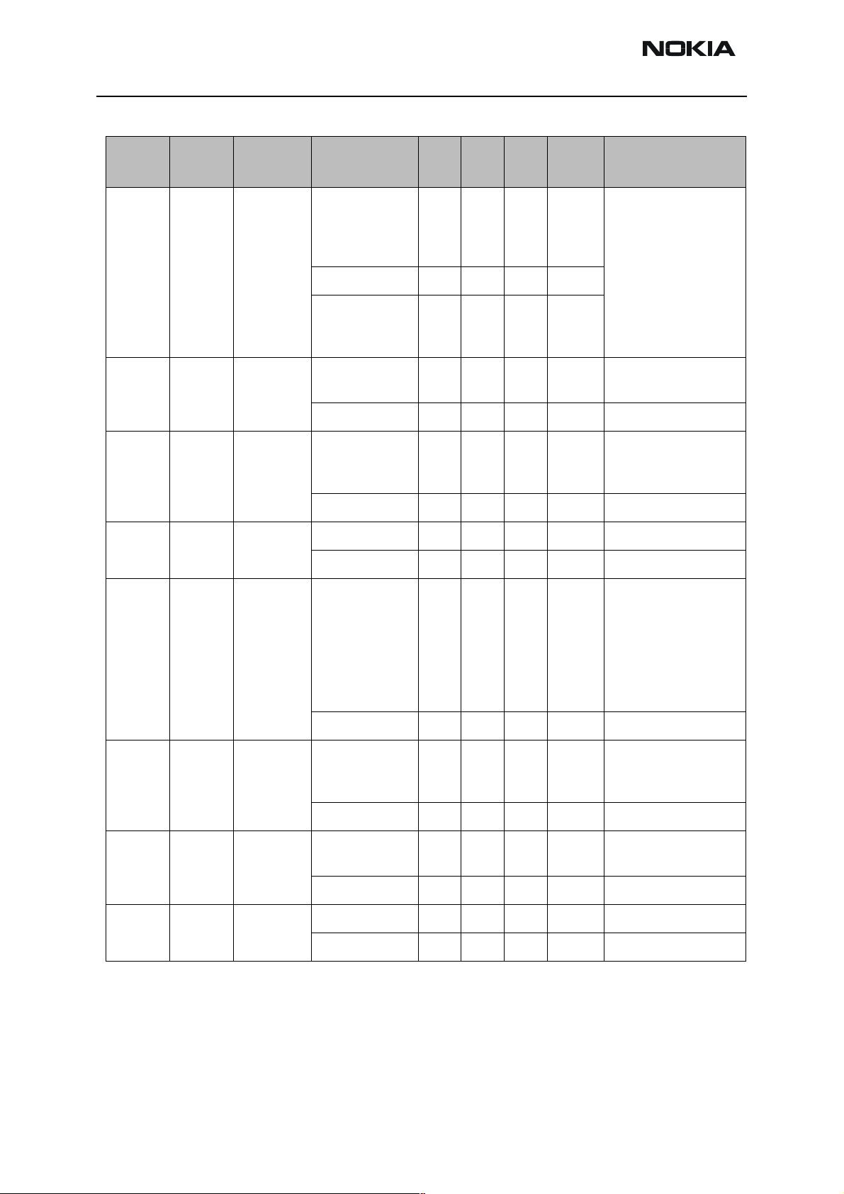
SIM Interface
UEM contains the SIM interface logic level shifting. SIM interface can be programmed to
support 3V and 1.8V SIMs. SIM supply voltage is selected by a register in the UEM. It is
only allowed to change the SIM supply voltage when the SIM IF is powered down.
The SIM power up/down sequence is generated in the UEM. This means that the UEM
generates the RST signal to the SIM. Also the SIMCardDet signal is connected to UEM.
The card detection is taken from the BSI signal, which detects the removal of the battery.
The monitoring of the BSI signal is done by a comparator inside UEM. The SIM interface
is powered up when the SIMCardDet signal indicates ”card in”. This signal is derived from
the BSI signal.
Table 23: SIMCARDet Detection
Parameter Variable Min Typ Max Unit
SIMCARDet, BSI comparator
Threshold
SIMCardDet, BSI comparator
Hysteresis (1)
The whole SIM interface locates in two chips: UPP and UEM.
Vkey 1.94 2.1 2.26 V
Vsimhyst 50 75 100 mV
The SIM interface in the UEM contains power up/down, port gating, card detect, data
receiving, ATR-counter, registers and level shifting buffers logic. The SIM interface is the
electrical interface between the Subscriber Identity Module Card (SIM Card) and mobile
phone (via UEM).
The data communication between the card and the phone is asynchronous half duplex.
The clock supplied to the card is in GSM system 1.083 MHz or 3.25 MHz.
Issue 1 04/03 Nokia Corporation Page 31
Page 32
NSB-9
System Module and User Interface CCS Technical Documentation
Figure 5: UPP/UEM SIM Interface Connections
GND
UPP
SIM
C5 C6 C7
C1 C2 C3
C8
C4
27p
27p
100p
100R
47R
100R
GND
SIMDATA
SIMIO
SIMCLK
SIMRST
VSIM
UEM
SIMClk
Data
SIMIF
register
SIMIO
SIMClk
Data
UIF Block
From Battery Type contact
UEM
digital
BSI
logic
UEMInt
CBusDa
CBusEnX
CBusClk
Page 32 Nokia Corporation Issue 1 04/03
Page 33

NSB-9
X
X
C
g
g
HSEAR
HSEAR
g
R
g
CCS Technical Documentation System Module and User Interface
System Connector
Table 24: DC- and System Connector features
Function Notes
Charging Pads for 2-wire charging in cradles
Audio - 4-wire fully differential stereo audio output
- 2-wire differential microphone input
Power supply for accessories 2.78V/70mA output to accessories
FBUS Standard FBUS
Figure 6: Charger plug socket and System Connector
PWB
1
14
e
Char
e
GND
Char
Shieldin
NC
ACI
Vout
Fbus R
NC
XMIC
Fbus T
XMI
External accessory regulator
An external regulator is needed for accessory power supply purposes. All ACI accessories
are requiring this power supply. Regulator input is connected to main battery voltage
VBAT and output is connected to System Connector VOUT pin. Regulator ON/OFF function is controlled with UPP GenI/O 0.
Table 25: Accessory Regulator Signals
Signal Min Nom Max Note
Vout 2.70V 2.78 2.86V Imax = 150mA
GenIO(0) 1.4 1.8 1.88
0.6
High (ON)
Low (OFF)
GND
Shieldin
HSEAR RHSEAR
Issue 1 04/03 Nokia Corporation Page 33
Page 34

NSB-9
Ω
Ω
System Module and User Interface CCS Technical Documentation
Figure 7: Accessory Power Supply Diagram
EN
VBATUPP
600
600Ω
600Ω600
@100MHz
Vout
Pin
System
Connector
GenI/O 0
Battery
1000 mAh Li-ion battery pack BLC-2 is used in NSB-9.
Table 26: BLC-2 Characteristics
Description of phenomenon Volts
Nominal discharge cut-off voltage 3.1V
Nominal battery voltage 3.6V
Nominal charging voltage 4.2V
Maximum charger output current 850 mA
Minimum charger output current 200 mA
Page 34 Nokia Corporation Issue 1 04/03
Page 35

NSB-9
CCS Technical Documentation System Module and User Interface
Table 27: Pin numbering of Battery Pack
Signal name Pin number Function
VBAT 1 Positive battery terminal
BSI 2 Battery capacity measurement (fixed resistor inside the battery pack)
BTEMP 3 Battery temperature measurement (measured by ntc resistor inside pack)
GND 4 Negative/common battery terminal
Figure 8: Battery Pack contents
The BSI fixed resistor value indicates type and default capacity of a battery. NTC-resistor
BTEMP measures the battery temperature.
Temperature and capacity information are needed for charge control. These resistors are
connected to BSI and BTEMP pins of battery connector. Phone has 100 kΩ pull-up resistors for these lines so that they can be read by A/D inputs in the phone.
Backup Battery
Backup battery is used in case when main battery is either removed or discharged.
Backup battery is used to keep real-time clock (RTC) running for minimum of 30 minutes.
Rechargeable backup battery (capacitor type) is connected between UEM VBACK and
GND. In UEM backup battery charging high limit is set to 3.2V. The cut-off limit voltage
(VBUCoff-) for backup battery is 2.0V. Backup battery charging is controlled by MCU by
writing into UEM register. Battery is not charged during power off.
Parameter
Test conditions
4(GND)
3(BTEMP)
Table 28: Back-up circuity
Symbol Min Typ Max Units
2(BSI)
1 (+)
Back-up battery voltage VBACK 2.43 3.3 V
Back-up battery cut-off limit V_BU
Charging voltage (VBAT ≥ 3.4V) VBU 3.1 3.2 3.3 V
Charging current I
V_BU
LIMVBU
COFF+
COFF-
2.04
1.94
150 500 mA
2.10
2.0
2.16
2.06
V
V
Issue 1 04/03 Nokia Corporation Page 35
Page 36

NSB-9
System Module and User Interface CCS Technical Documentation
LCD & Keypad Illumination
In NSB-9 white LEDs are used for LCD and keypad illumination. For LCD illumination
three LEDs are used and for keypad three in both qwerty sides and four in ITU-T keypad
(0, 1, 2, 3, 4, 5, 6, 7, 8, 9, * and #), and three in engine control keys. Engine LEDs are controlled by UEM KLIGHT and DLIGHT signals. Flip LEDs are controller by flip MCU, according to flip serial interface messages.
Figure 9: Engine qwerty keypad LED connection
VBAT
22R
VBAT
Engine qwerty
keypad LEDs
470R
330R
KLIGHT
Current through LEDs is controlled by transistor circuitry. External transistor driver circuitry is used as constant current source in order to prevent any change in the battery
voltage to be seen as varying LED brightness.
Page 36 Nokia Corporation Issue 1 04/03
Page 37

NSB-9
CCS Technical Documentation System Module and User Interface
Figure 10: Engine qwerty keypad LED connection
LCD
LCD and engine SW & control keys LEDs are driven in serial mode (3 + 3 connected parallel) by a LED driver to achieve stable and bright backlightning. 33R resistor is used to
define the proper current for LCD backlightning (about 16mA). The feedback signal Vfb
(voltage across 33R) is used to control the current. LED driver will increase or decrease
the output voltage for LEDs to keep the current stable. If current path through LCD LEDs
is open, current is at its maximum and it flows through the three other LEDs
NSB-9 has 130 x 130 8bpp (bits per pixel) passive matrix colour STN display. Interface is
using 9 bit data transfer. D/C bit is set during each transmitted byte.
UPP drives the CSX pin low and starts by setting the D/C-bit (data/command) to SDA. The
bit is read by the display on the first rising edge of CLK. On the next falling edge of CLK
the MSB data bit (D7) is set to SDA by the engine. On the next falling edge of CLK the
next bit (D6) is set to SDA. This continues until all 8 bits have been transmitted.
Issue 1 04/03 Nokia Corporation Page 37
Page 38

NSB-9
System Module and User Interface CCS Technical Documentation
ACI
(Accessory Control Interface) is a point-to-point, bi-directional serial bus. ACI has three
main features:
• Insertion and removal detection of an accessory device
• Identify and authenticate the connected accessory
• Data bus for accessory control
The accessories are detected by the HEADINT signal when the accessory is inserted.
Normally when no accessory is present, the 100k pull-up resistor pulls up the HEADINT
signal to VFLASH1. When the accessory is inserted, the external ”insertion and removal”
resistor works as a voltage devider and decreases the voltage level below the threshold
Vhead. Thereby the comparator output will be changed to high state causing an interrupt.
When the accessory is removed, the voltage level of HEADINT increases again to
VFLASH1. This voltage level is higher than the threshold of the comparator and thereby
its output will be changed to low state. This change causes an interrupt.
Those HEADINT interrupts are initiated by the accessory detection or removal sequence.
External Audio
NSB-9 is designed to support fully differential external audio accessory connection by
using Pop-Port system connector. Pop-Port connector has serial data bus called ACI
(Accessory Control Interface) for accessory insertion and removal detection, utilizing,
identification and authentication. ACI line is also used for accessory control purposes.
Audio support with Pop-Port system connector:
• 2-wire differential mic input
• 4-wire fully differential stereo audio output (used also as an FM-radio antenna)
External Microphone Connection
The external microphone input is fully differential and lines are connected to the UEM
microphone input MIC2P/N.
The UEM (MICB2) provides bias voltage. Microphone input lines are ESD protected. Creating a short circuit between the headset microphone signals (with headset button) generates the hook signal. When the accessory is not connected, the UEM resistor pulls up
the HookInt signal. When the accessory is inserted and the microphone path is biased the
HookInt signal decreases to 1.8V due to the microphone bias current flowing through the
resistor. When the button is pressed the microphone signals are connected together, and
the HookInt input will get half of micbias dc value 1.1 V. This change in DC level will
Page 38 Nokia Corporation Issue 1 04/03
Page 39

NSB-9
CCS Technical Documentation System Module and User Interface
cause the HookInt comparator output to change state, in this case from 0 to 1. The button can be used for answering incoming calls and then ending them. The button can be
used for initiating outgoing calls, if voice tags are saved for dialing.
Figure 11: External microphone connection
Hookint
MICB2
UEM
MIC2P
MIC2N
EMC/ESD
Components
XMICP
XMICN
Issue 1 04/03 Nokia Corporation Page 39
Page 40

NSB-9
System Module and User Interface CCS Technical Documentation
External Earphone Connections
Figure 12: System connector
Internal Audio
Internal Microphone
The internal microphone module and holder is mounted into the B-cover. Microphone is
omni directional. The internal microphone is connected to the UEM microphone input
MIC1P/N. The microphone input is asymmetric and microphone bias is provided by the
UEM MIC1B. The microphone input on the UEM is ESD protected. Spring contacts are
used to connect the microphone contacts to the main PWB.
UEM
MIC1P
MIC1N
Figure 13: Internal microphone connections
600
2k2
2x33nF
2x2k2
ΩΩΩΩ
@100MHz
MICB1
4u7
100nF
Page 40 Nokia Corporation Issue 1 04/03
Page 41

NSB-9
CCS Technical Documentation System Module and User Interface
Internal Speaker
The internal earpiece is mounted into the LCD metal frame. The earpiece is a dynamic
earpiece with a 32 ohm impedance. The earpiece is low impedance one since the sound
pressure is to be generated using current and not voltage as the supply voltage is
restricted to 2.7V. The earpiece is driven directly by the UEM. The earpiece driver in UEM
is a bridge amplifier.
Figure 14: Internal speaker
connections
UEM
EARP
EARN
2x1000
ΩΩΩΩ
@100MHz
8mm PICO
5140247
27p
Integrated Hands Free
Integrated Handsfree (IHF) makes it possible to keep the phone for example on desk and
keep both hands free. When IHF mode is activated, internal microphone is used as in HPmode and IHF speaker is used instead of earpiece.
The FM-radio can be listened from the IHF speaker as well, if a headset is connected
(FM-radio antenna).
The stereo audio amplifier supports four inputs and three outputs. It is capable of delivering 340mW of continuous averahe power into a mono 8Ohm bridged-tied load and
25mW per channel of continuous average power into stereo 32Ohm loads (when using
3V supply voltage). Stereo signal from FM-radio is connected to Rin and Lin inputs, and
XEAR signal from UEM is connected to PhoneInHS input of stereo audio amplifier. Phone
IHF line includes discrete RC high-pass filtering in order to cut off low frequencies from
IHF speaker. SPKROut lines are connected to IHF speaker. PhoneInIHF to SPKROut path
has fixed 12dB gain.
27p
Issue 1 04/03 Nokia Corporation Page 41
Page 42

NSB-9
System Module and User Interface CCS Technical Documentation
Figure 15: IHF connections
TEA5767
VAFR
VAFL
UEM
MIC3
XEAR
Memory Block
Stereo
Amplifier
Rin
Lin
Phone_in
IHF
SPKRout -
SPKRout +
IHF
For the MCU UPP includes ROM, 2 kbytes, that is used mainly for boot code of MCU. To
speed up the MCU operation small 64 byte cache is also integrated as a part of the MCU
memory interface. For program memory 8Mbit (512k x 16bit) PDRAM is integrated into
UPP, and 8Mbit external SRAM is in separate COMBO MEMORY chip. RAM block can also
be used as data memory and it is byte addressable. RAM is mainly for MCU purposes but
also DSP has also access to it if needed.
MCU code is stored into external flash memory, which is in a combo memory chip. The
size of the flash is 128Mbit (8M x 16bit). The NSB-9 baseband supports a burst mode
flash with multiplexed address/data bus. Access to the flash memory is performed as 16bit access. The flash has Read While Write capabilities which makes the emulation of
EEPROM within the flash easy.
Security
The phone flash program and IMEI code are software protected using an external security device that is connected between the phone and a PC.
Page 42 Nokia Corporation Issue 1 04/03
Page 43

NSB-9
CCS Technical Documentation System Module and User Interface
Production / After Sales Interface
Test pads are placed on engine PWB bottom side for service and production trouble
shooting purposes.
The standard 5 pin test pattern is shown in figure below. NSB-9 has two pins for FMradio testing. The pins are connected in parallel with two system connector audio output
lines (HSEAR P and HSEAR R N). The FM radio can be tested between those lines.
Figure 16: Flash and FM-radio test connection
FM Radio test
FM Radio test
(audio output)
FBUS_RX
FBUS_TX
(audio output)
GND
MBUS
VPP
Issue 1 04/03 Nokia Corporation Page 43
Page 44

NSB-9
System Module and User Interface CCS Technical Documentation
[This page intentionally left blank.]
Page 44 Nokia Corporation Issue 1 04/03
 Loading...