

Page 1

CCS Technical Documentation
NSB-9 Series Transceivers
Troubleshooting Instructions
Issue 1 04/03 Nokia Corporation
Page 2
NSB-9
Troubleshooting Instructions CCS Technical Documentation
[This page left intentionally blank]
Page 2 Nokia Corporation Issue 1 04/03
Page 3

NSB-9
CCS Technical Documentation Troubleshooting Instructions
Table of Contents
Page No
RF Troubleshooting ....................................................................................................... 4
Introduction ..................................................................................................................4
EQUIPMENT NEEDED:.......................................................................................... 4
USEFUL HINTS ....................................................................................................... 4
TROUBLESHOOTING IN CASE OF RF TUNING FAIL ........................................5
Channel Select Filter Calibration .............................................................................. 5
RX Calibration .......................................................................................................... 5
RX AM Suppression Calibration .............................................................................. 5
RX Band Filter Response Compensation.................................................................. 5
TX Power Level Tuning............................................................................................ 5
TX IQ Tuning............................................................................................................ 5
TX 850 Troubleshooting ..............................................................................................6
Phoenix commands ................................................................................................... 6
TX1900 TROUBLESHOOTING ................................................................................9
Phoenix commands ................................................................................................... 9
RX850 troubleshooting ..............................................................................................12
Phoenix commands ................................................................................................. 12
RX1900 Troubleshooting ..........................................................................................15
Phoenix commands ................................................................................................. 15
Figures of signals and voltages in testpoints .............................................................18
FM Radio Troubleshooting ........................................................................................35
Introduction ............................................................................................................. 35
EQUIPMENT NEEDED......................................................................................... 35
FM RADIO SCHEMATICS ......................................................................................36
FM Radio layout...................................................................................................... 39
REFERENCE MEASUREMENT RESULTS ........................................................ 42
Baseband Troubleshooting........................................................................................... 45
PWB Test points ........................................................................................................45
Troubleshooting steps ................................................................................................51
Main troubleshooting tree ..........................................................................................53
Phone is dead .............................................................................................................55
Flash faults .................................................................................................................56
Phone is jammed ......................................................................................................58
Charging fault ............................................................................................................60
SIM card fault ............................................................................................................61
Audio faults ...............................................................................................................62
Display faults .............................................................................................................70
Keypad faults .............................................................................................................72
Flip faults ...................................................................................................................76
FM Radio doesn’t work .............................................................................................78
Issue 1 04/03 Nokia Corporation Page 3
Page 4
NSB-9
Troubleshooting Instructions CCS Technical Documentation
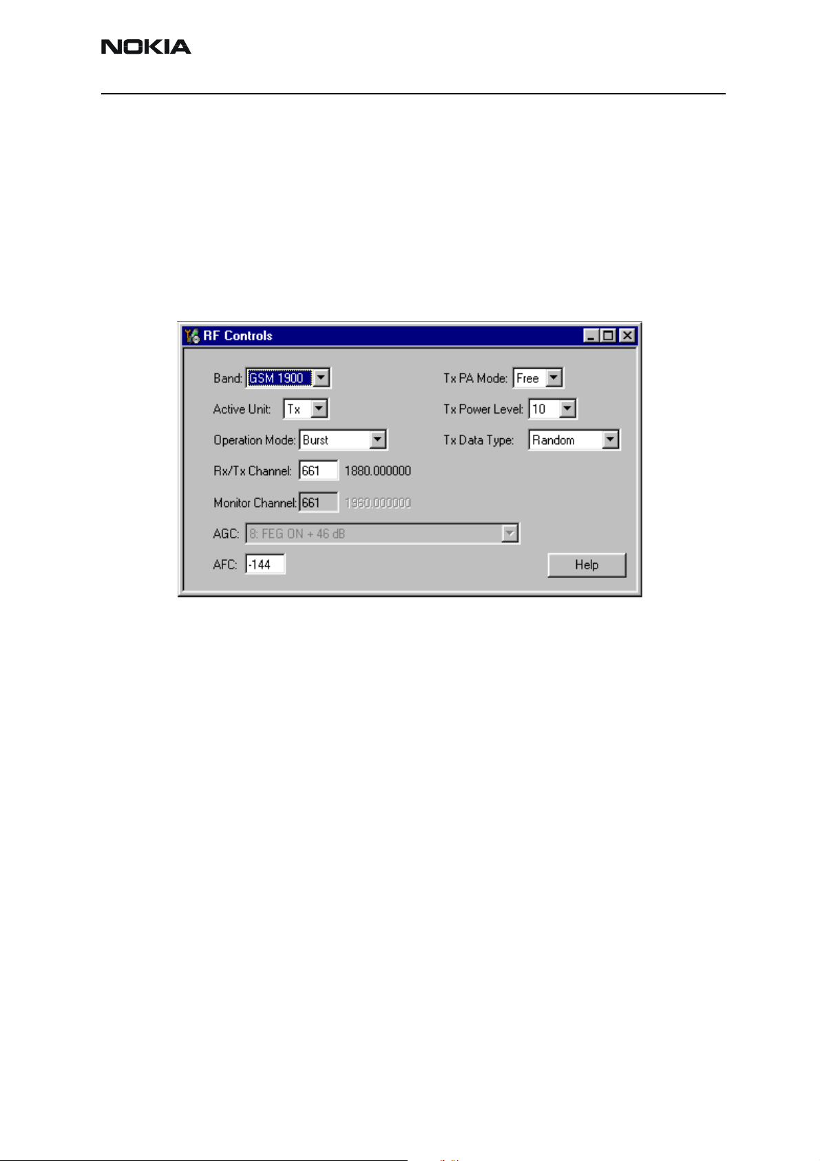
RF Troubleshooting
Introduction
This document describes the methods of RF troubleshooting for Iris NSB-9 transceiver.
Fault finding charts of the most common fails are included in this document. Arrows are
marked with 9 (OK) and 8 (NOT OK), respectively. Measurement equipment is marked as:
DMM Digital Multimeter
OSC Oscilloscope
SA Spectrum Analyzer
Figures of typical signals and voltages at each testpoint are described in Chapter 8.
Location of testpoints are described in Chapters 9 and 10.
EQUIPMENT NEEDED:
NSB-9 module jig MJS-48, power and DAU-9S cables
DC power supply 3.9 VDC >3A
Radio Communication Tester with GSM850/1900 option
Spectrum analyzer and probe with frequency range up to 4 GHz
Digital multimeter (DMM)
Oscilloscope with 10:1 probe
PC with Phoenix software
USEFUL HINTS
Sometimes it is difficult to get reliable measurement results at high frequencies
(500...4000 MHz) because of probe properties etc. If measurement results of faulty
phone don't correspond to the results shown in this document it may be useful to measure a reference phone and finally, compare the results.
Special attention shall be paid with internal antenna. Visual inspection of antenna module (shape of radiator metal) is needed to verify that antenna is GSM850/1900 antenna not GSM900/1800 used in similar European product. Both antennas behave very similarly in MJF-32 jig so it may be impossible to distinguish them by doing measurements
over air interface.
Page 4 Nokia Corporation Issue 1 04/03
Page 5

NSB-9
CCS Technical Documentation Troubleshooting Instructions
TROUBLESHOOTING IN CASE OF RF TUNING FAIL
Channel Select Filter Calibration
Calibration is done using internal calibration circuit (UEM sends and receives a test signal to/from Hagar). VCO (G650), RX-bandfilters (Z501, Z551) and TX-filter/balun (Z700,
T700) don't have any effect to the Channel Select Filter Calibration. Instead, baseband
shall be functional (=VCTCXO G660 is running). Any failure in Hagar, its supply voltages
or RX/TX IQ-lines may cause this calibration to be failed.
If baseband works and there are not any visible cause around Hagar (missing or broken
components etc.), Hagar shall be replaced at first place.
RX Calibration
The most probably reason for this is lack of gain in receiver chain. Check rx chain according to RX850/1900 fault finding charts. In GSM850 RX, components Z520, V500 and
Z501 should be checked. In GSM1900 RX, components Z520, V550 and Z551 should be
checked.
If signal seems to pass rx chains with adequate gain, VCO function shall be checked. It is
also possible that signal passes rx chain to Hagar and VCO is functional but signal
doesn't appear in RX IQ-lines. In this case, Hagar shall be replaced.
RX AM Suppression Calibration
RX AM Suppression Calibration limits (LOPI, LOMI, LOPQ and LOMQ) are so wide that the
calibration results can't exceed the limits. Instead, RSSI value measured after tuning may
be too high. Also in this case, replacing Hagar may improve the result.
RX Band Filter Response Compensation
If RX Calibration results are ok but this compensation fails, the most probably reason for
this is lack of gain (or too big gain) in receiver chain in some frequency. Check rx chain
according to RX850/1900 fault finding charts. Retest rx chain also in low and high channels. In GSM850 RX, components Z520 and Z501 should be checked. In GSM1900 RX,
components Z520 and Z551 should be checked.
TX Power Level Tuning
The most likely reason for this is lack of gain in transmitter chain. Check tx chain according to TX850/1900 fault finding charts. In GSM850 TX, components Z500, L750, N700
and Z700 should be checked. In GSM1900 TX, components Z500, L750, N700 and T700
should be checked.
If signal seems to pass tx chains with adequate gain, VCO function shall be checked. It is
also possible that signal doesn't appear in TX IQ-lines. In this case, baseband shall be
checked.
TX IQ Tuning
TX IQ tuning fails, if IQ-spikes in the spectrum can't be tuned low enough. If replacing
Hagar doesn't help with this issue, VCO component (G650) and components around it
Issue 1 04/03 Nokia Corporation Page 5
Page 6
NSB-9
Troubleshooting Instructions CCS Technical Documentation
shall be checked.
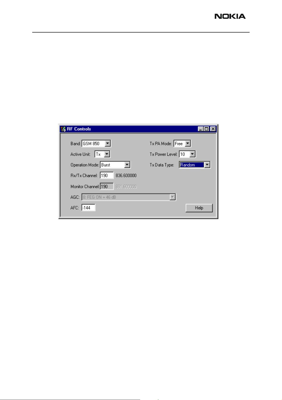
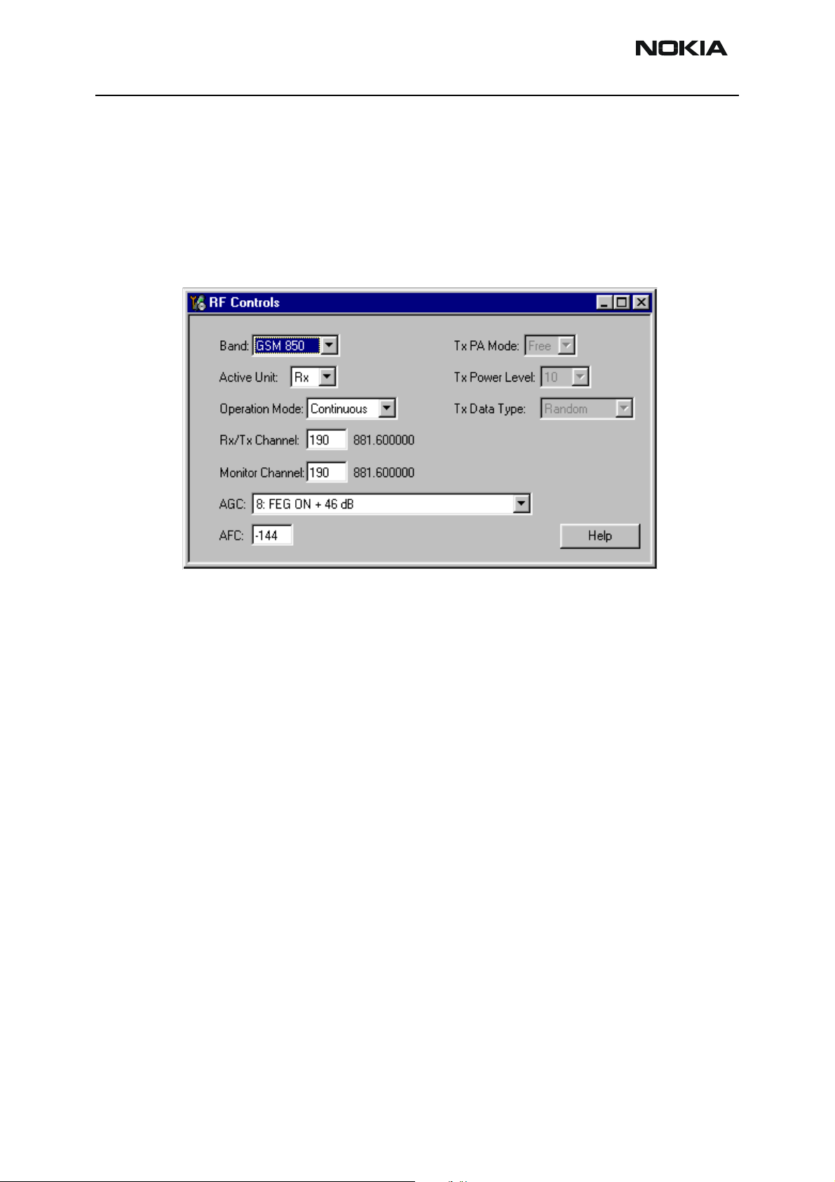
TX 850 Troubleshooting
Phoenix commands
RF Controls ⇒ Band GSM 850 TX ⇒ Burst mode
Channel 190 ⇒ TX Power Level 10
TX PA Mode Free ⇒ TX Data Random
Page 6 Nokia Corporation Issue 1 04/03
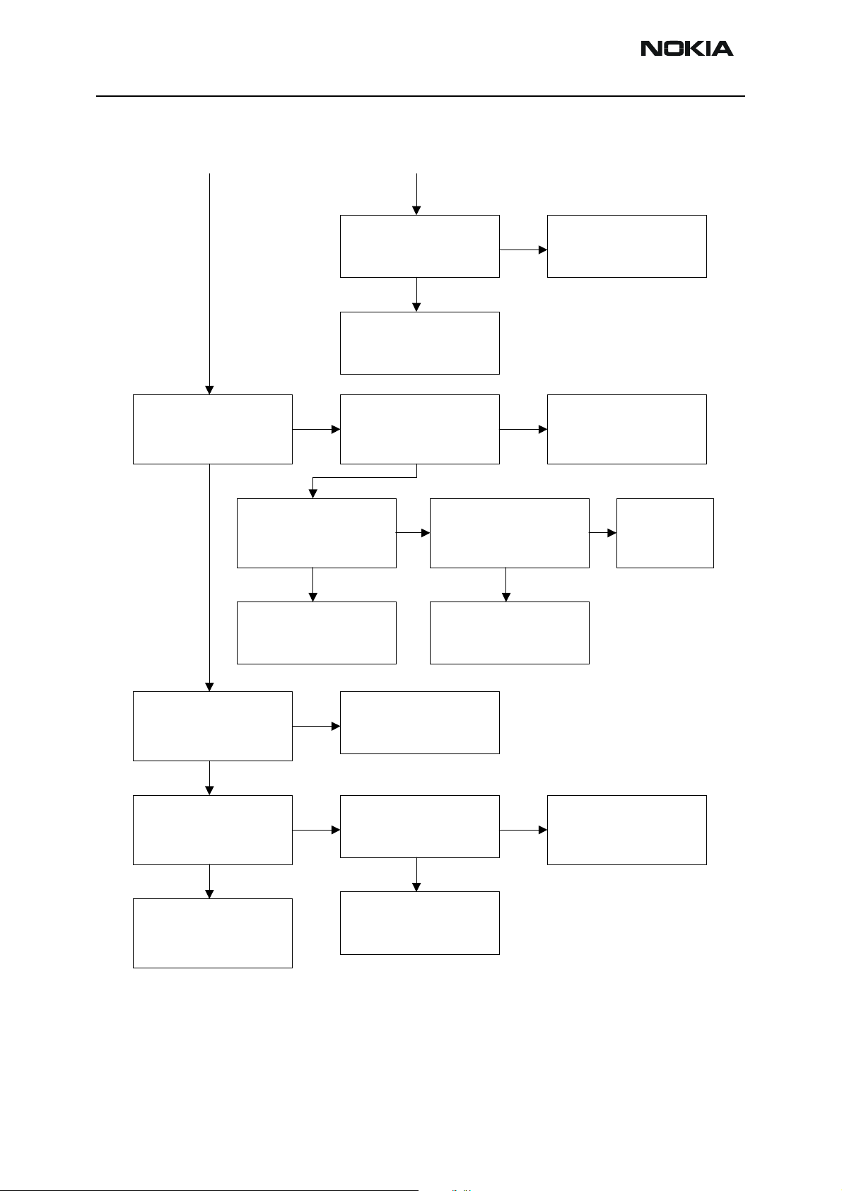
Page 7
NSB-9
CCS Technical Documentation Troubleshooting Instructions
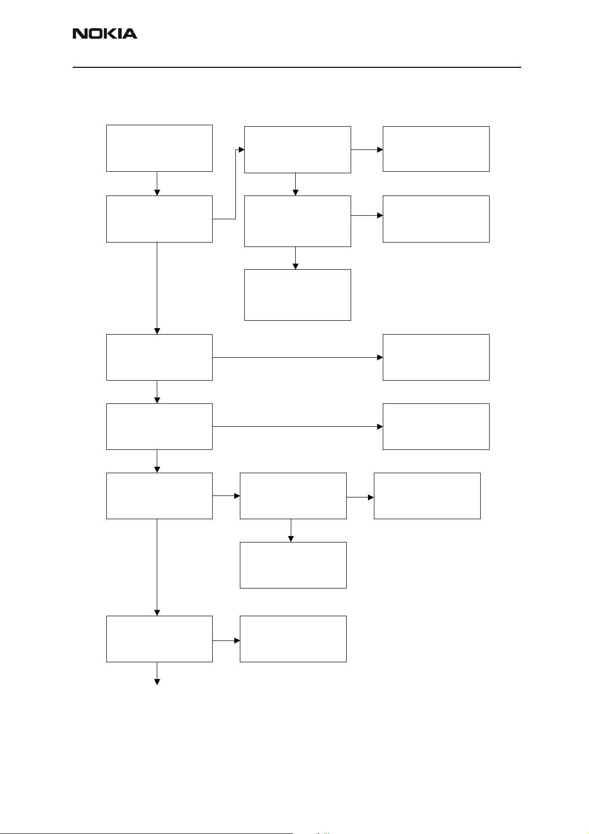
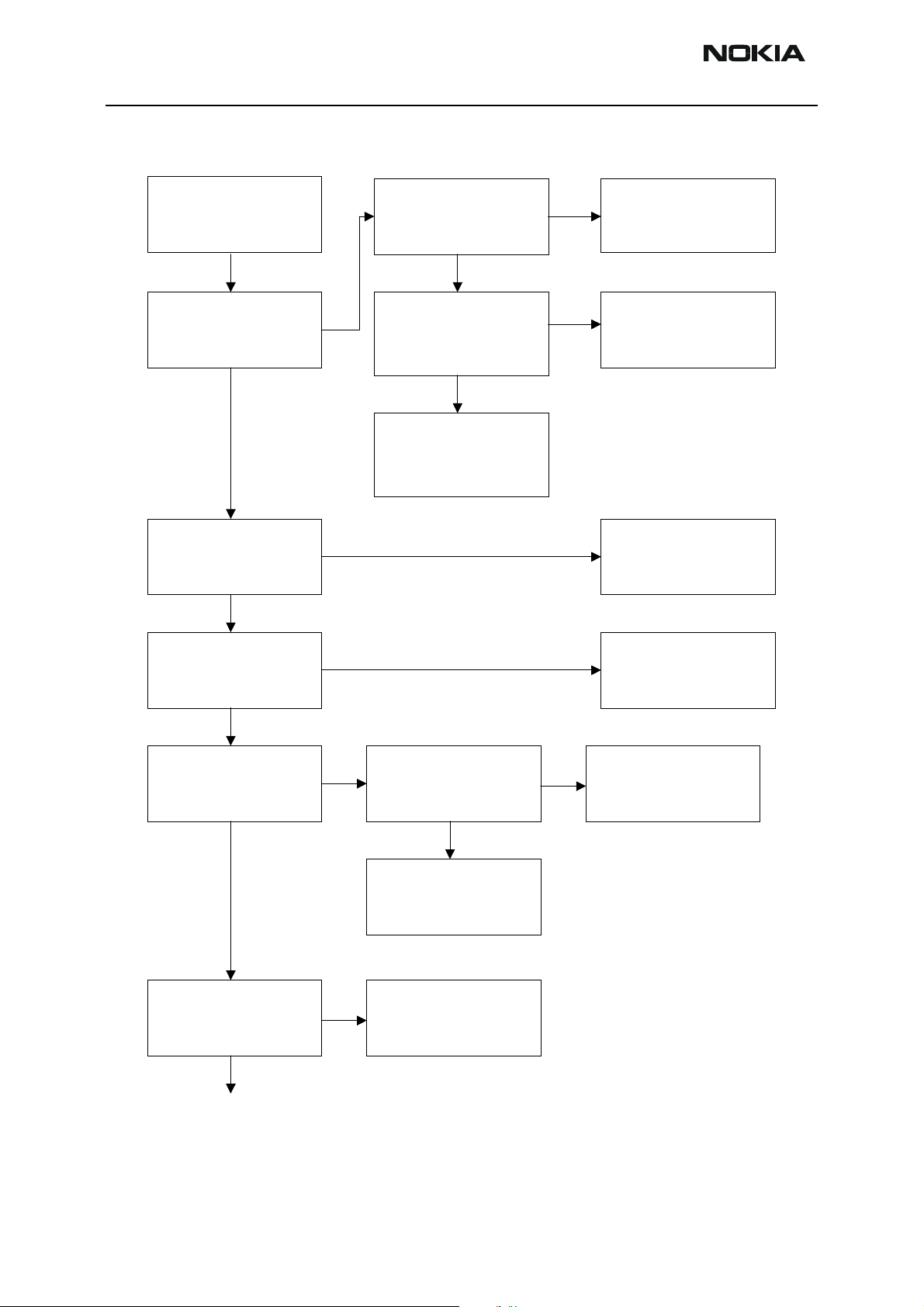
Figure 1: Fault finding chart, TX850
Check VCTCXO
output signal at TP20
26 MHz
9
Check TX IQ signals
at TP21
9
Check TX modulator
output signal at TP24
836.6 MHz
OSC
OSC
SA
8
8
8
Check VCTCXO
supply voltage at TP3
2.78 VDC ± 3%
DMM
9
Check VCTCXO
control voltage at
TP13
1.1 VDC ± 200 mV
9
Change VCTCXO
G660
Check SHF VCO
output signal at TP40
3346.4 MHz
DMM
SA
8
8
8
Start baseband
troubleshooting (UEM)
Start baseband
troubleshooting (UEM)
Start baseband
troubleshooting (UEM)
8
Check VCO supply
voltage at TP7:
2.78 VDC ± 3%
DMM
9
9
DMM
Check Hagar ASIC
supply voltages at
TP4, TP5, TP6, TP8:
2.78 VDC ± 3%
TP10: 1.35 VDC ± 2%
TP1: 4.75 VDC ± 3.2%
9
Check VCO control
1.1 VDC ± 200 mV
Change
Hagar ASIC
N600
8
troubleshooting (UEM)
9
voltage at TP41:
DMM
89
Change
8
SHF VCO
G650
Start baseband
Issue 1 04/03 Nokia Corporation Page 7
Page 8
NSB-9
Troubleshooting Instructions CCS Technical Documentation
99
Check PA output
signal at TP60
836.6 MHz
9
TP51, SCLK TP52,
8
SA
Check PA control
voltage at TP27
VBATT (∼3.9 VDC)
9
Change PA
N700
Check SDATA at
SLE TP53
9
Change
Hagar ASIC
N600
Check PA supply
voltage at TP9
9
OSC
8
signal at TP23
8
OSC
DMM
8
Check TXC
9
Change
Hagar ASIC
N600
Start baseband
troubleshooting (UPP)
Check VBATT path
from battery connector
to PA
OSC
Start baseband
8
troubleshooting
(UEM)
Check coupler output
signal at TP61
836.6 MHz
9
Check TX output
signal at TP30
836.6 MHz
9
TX is ok
SA
SA
8
8
Change
coupler
L750
Check antenna switch
control signal at TP62
2.78 V squarewave
OSC
9
Change
antenna
switch Z500
8
Change Hagar
ASIC
N600
Page 8 Nokia Corporation Issue 1 04/03
Page 9
NSB-9
CCS Technical Documentation Troubleshooting Instructions
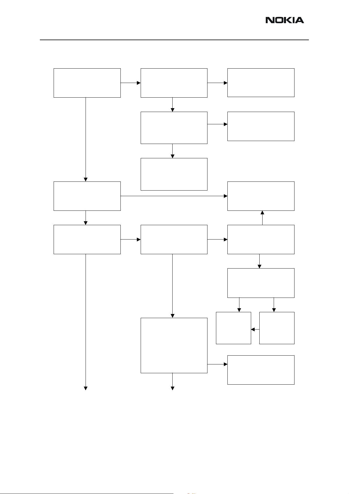
TX1900 TROUBLESHOOTING
Phoenix commands
RF Controls ⇒ Band GSM 1900 TX ⇒ Burst mode
Channel 661 ⇒ TX Power Level 10
TX PA Mode Free ⇒ TX Data Random
Issue 1 04/03 Nokia Corporation Page 9
Page 10
NSB-9
Troubleshooting Instructions CCS Technical Documentation
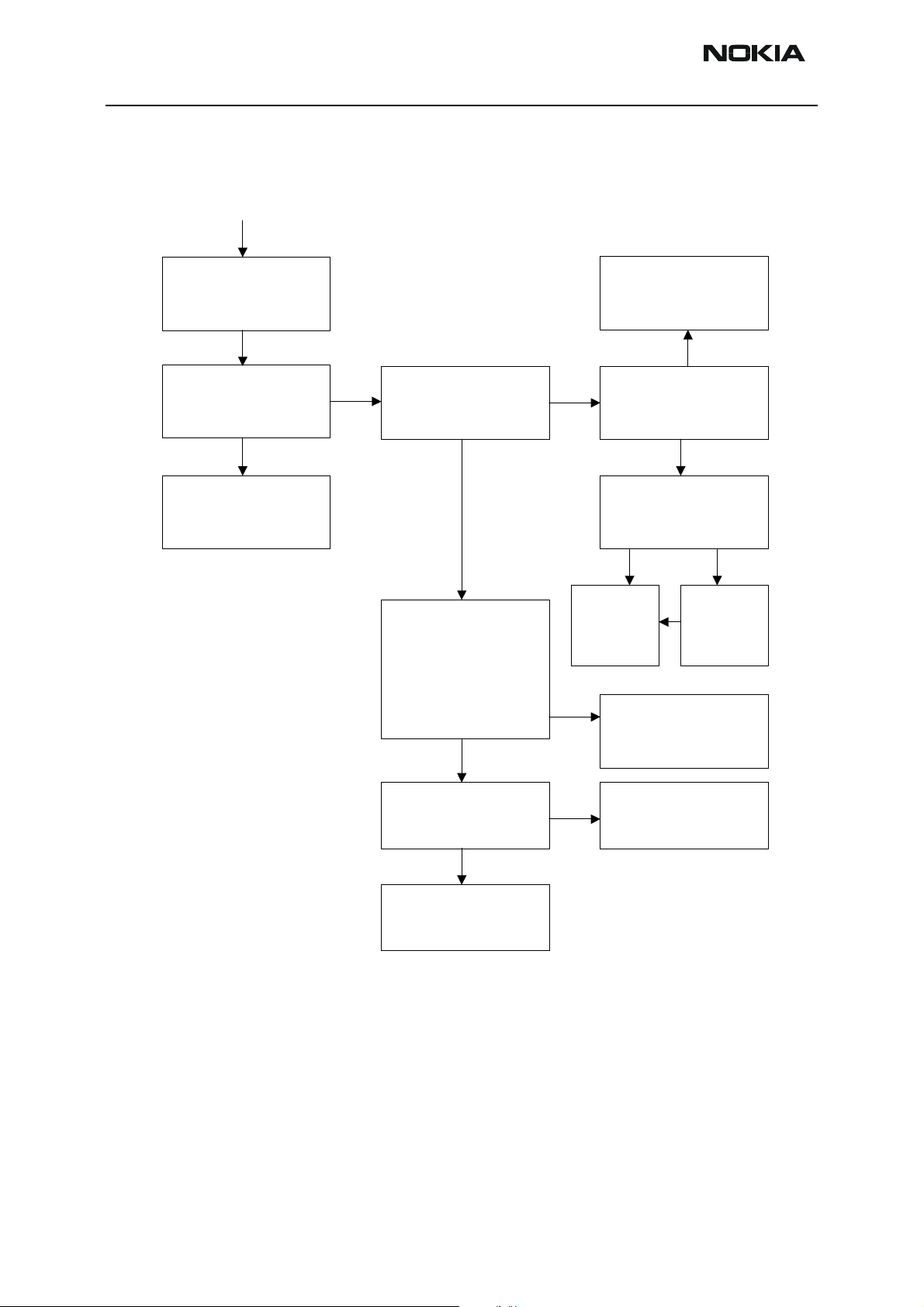
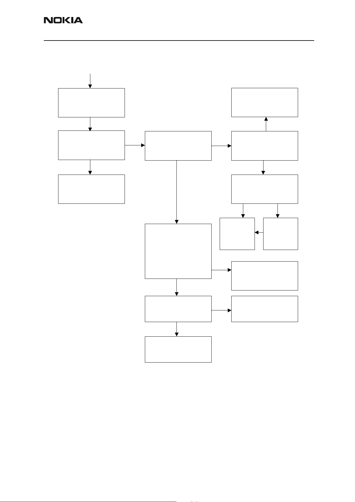
Figure 2: Fault finding chart, TX1900
Check VCTCXO
output signal at TP20
26 MHz
9
Check TX IQ signals
at TP21
9
Check TX modulator
output signal at TP22
1880 MHz
OSC
OSC
SA
8
8
8
Check VCTCXO
supply voltage at TP3
2.78 VDC ± 3%
DMM
9
Check VCTCXO
control voltage at
TP13
1.1 VDC ± 200 mV
9
Change VCTCXO
G660
Check SHF VCO
output signal at TP40
3760 MHz
DMM
SA
8
8
8
Start baseband
troubleshooting (UEM)
Start baseband
troubleshooting (UEM)
Start baseband
troubleshooting (UEM)
Check VCO supply
voltage at TP7:
2.78 VDC ± 3%
8
DMM
9
9
DMM
Check Hagar ASIC
supply voltages at
TP4, TP5, TP6, TP8:
2.78 VDC ± 3%
TP10: 1.35 VDC ± 2%
TP1: 4.75 VDC ± 3.2%
9
Check VCO control
voltage at TP41:
2.7 VDC ± 200 mV
89
Change
Hagar ASIC
N600
8
Start baseband
troubleshooting (UEM)
8
9
DMM
Change
SHF VCO
G650
Page 10 Nokia Corporation Issue 1 04/03
Page 11
NSB-9
CCS Technical Documentation Troubleshooting Instructions
99
Check PA output
signal at TP25
1880 MHz
9
TP51, SCLK TP52,
8
SA
Check PA control
voltage at TP26
VBATT (∼3.9 VDC)
9
Change PA
N700
Check SDATA at
SLE TP53
9
Change
Hagar ASIC
N600
Check PA supply
voltage at TP9
9
OSC
8
signal at TP23
8
OSC
DMM
8
Check TXC
9
Change
Hagar ASIC
N600
Start baseband
troubleshooting (UPP)
Check VBATT path
from battery connector
to PA
OSC
Start baseband
8
troubleshooting
(UEM)
Check coupler output
signal at TP28
1880 MHz
9
Check TX output
signal at TP30
1880 MHz
9
TX is ok
SA
SA
8
8
Change
coupler
L750
Check antenna switch
control signal at TP29
2.78 V squarewave
OSC
9
Change
antenna
switch Z500
8
Change Hagar
ASIC
N600
Issue 1 04/03 Nokia Corporation Page 11
Page 12
NSB-9
Troubleshooting Instructions CCS Technical Documentation
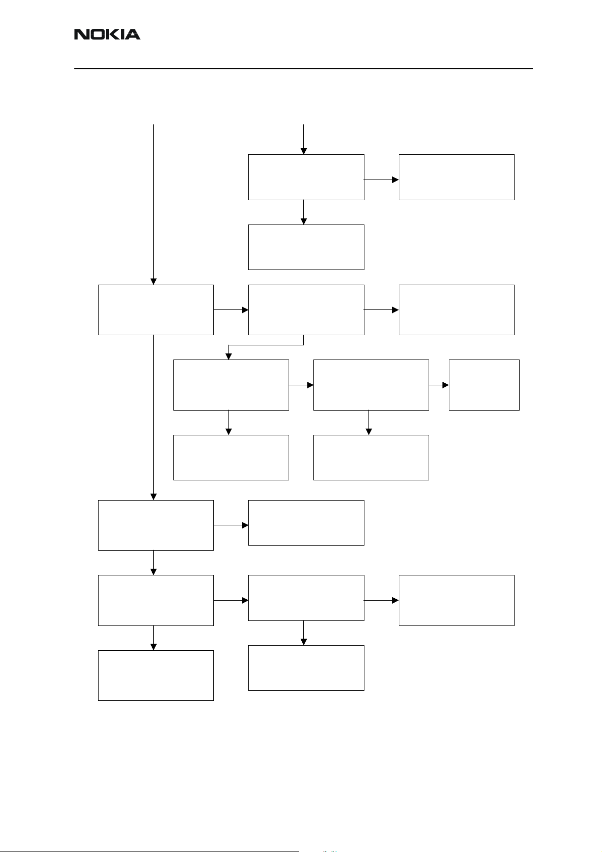
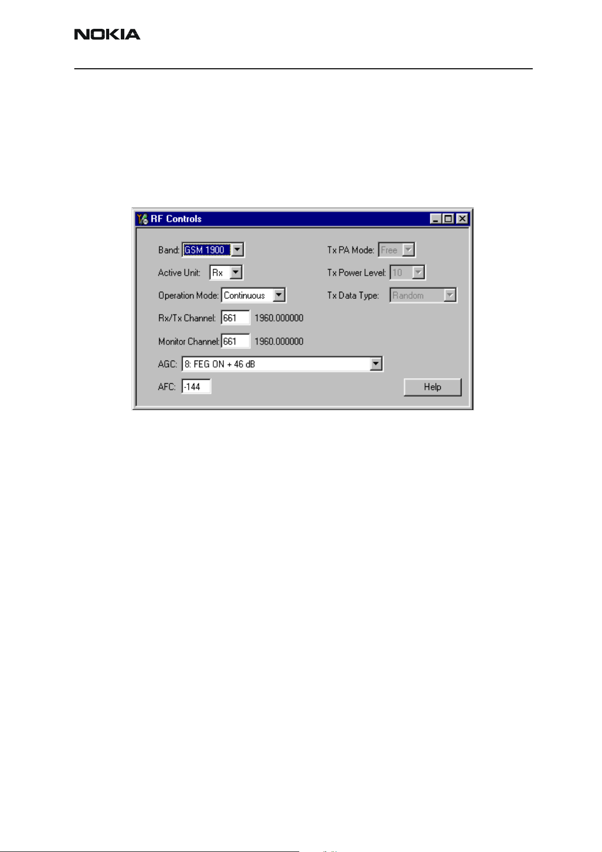
RX850 troubleshooting
Phoenix commands
RF Controls ⇒ Band GSM 850 RX ⇒ Continuous mode
Channel 190 ⇒ AGC 8 FEG ON + 46 dB
Page 12 Nokia Corporation Issue 1 04/03
Page 13
NSB-9
CCS Technical Documentation Troubleshooting Instructions
Figure 3: Fault finding chart, RX850
Apply input signal
881.667 MHz
-50 dBm
9
Check VCTCXO
output signal at TP20
26 MHz
OSC
9
Check RX signal at
antenna switch output
TP63
881.667 MHz
9
Check RX signal at
dual filter output TP64
881.667 MHz
SA
SA
8
8
8
Check VCTCXO
supply voltage at TP3
2.78 VDC ± 3%
DMM
9
Check VCTCXO
control voltage at
TP13
1.1 VDC ± 200 mV
DMM
9
Change VCTCXO
G660
8
8
Start baseband
troubleshooting (UEM)
Start baseband
troubleshooting (UEM)
Change antenna
switch Z500
Change dual filter
Z520
9
Check RX signal at
LNA output TP66
881.667 MHz
9
Check RX signal at
filter output TP68
881.667 MHz
9
SA
SA
Check LNA voltages
8
8
at TP65 1 VDC
TP67 2.6 VDC
Check LNA V500 and
other components
around it
Change filter Z501
9
DMM
If R501 and R502 are
8
ok, change Hagar
ASIC N600
Issue 1 04/03 Nokia Corporation Page 13
Page 14
NSB-9
Troubleshooting Instructions CCS Technical Documentation
9
Apply input signal
881.667 MHz
-90 dBm
9
OSC
Check RX IQ signal at
TP37
9
Start baseband
troubleshooting (UEM)
Check SHF VCO
8
output signal at TP40
3526.4 MHz
Check Hagar ASIC
supply voltages at
TP4, TP5, TP6, TP8:
2.78 VDC ± 3%
TP10: 1.35 VDC ± 2%
TP1: 4.75 VDC ± 3.2%
9
SA
DMM
Start baseband
troubleshooting (UEM)
8
Check VCO supply
voltage at TP7:
2.78 VDC ± 3%
Check VCO control
voltage at TP41:
1.8 VDC ± 200 mV
8 9
Change
Hagar ASIC
N600
8
Start baseband
troubleshooting (UEM)
8
8
DMM
9
DMM
Change
SHF VCO
G650
9
Check SDATA at
TP51, SCLK TP52,
SLE TP53
9
Change
Hagar ASIC
N600
OSC
8
Start baseband
troubleshooting (UPP)
Page 14 Nokia Corporation Issue 1 04/03
Page 15
NSB-9
CCS Technical Documentation Troubleshooting Instructions
RX1900 Troubleshooting
Phoenix commands
RF Controls ⇒ Band GSM 1900 RX ⇒ Continuous mode
Channel 661 ⇒ AGC 8 FEG ON + 46 dB
Issue 1 04/03 Nokia Corporation Page 15
Page 16
NSB-9
Troubleshooting Instructions CCS Technical Documentation
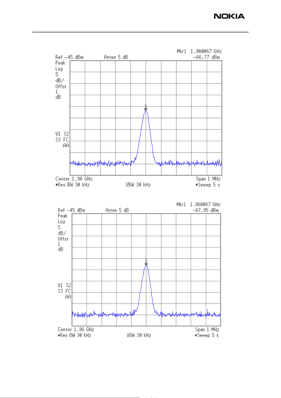
Figure 4: Fault finding chart, RX1900
Apply input signal
1960.067 MHz
-50 dBm
9
Check VCTCXO
output signal at TP20
26 MHz
OSC
9
Check RX signal at
antenna switch output
TP31
1960.067 MHz
SA
9
8
8
Check VCTCXO
supply voltage at TP3
2.78 VDC ± 3%
DMM
9
Check VCTCXO
control voltage at
TP13
1.1 VDC ± 200 mV
DMM
9
Change VCTCXO
G660
8
8
Start baseband
troubleshooting (UEM)
Start baseband
troubleshooting (UEM)
Change antenna
switch Z500
Check RX signal at
dual filter output TP32
1960.067 MHz
9
Check RX signal at
LNA output TP33
1960.067 MHz
9
Check RX signal at
filter output TP36
1960.067 MHz
9
SA
SA
SA
8
Check LNA voltages
8
8
at TP34 2.6 VDC
TP35 0 VDC
Check LNA V550 and
other components
around it
Change filter Z551
9
DMM
Change dual filter
If R551 is ok, change
8
Hagar ASIC N600
Z520
Page 16 Nokia Corporation Issue 1 04/03
Page 17
NSB-9
CCS Technical Documentation Troubleshooting Instructions
9
Apply input signal
1960.067 MHz
-90 dBm
9
OSC
Check RX IQ signal at
TP37
9
Start baseband
troubleshooting (UEM)
Check SHF VCO
8
output signal at TP40
3920 MHz
Check Hagar ASIC
supply voltages at
TP4, TP5, TP6, TP8:
2.78 VDC ± 3%
TP10: 1.35 VDC ± 2%
TP1: 4.75 VDC ± 3.2%
9
SA
DMM
Start baseband
troubleshooting (UEM)
8
Check VCO supply
voltage at TP7:
2.78 VDC ± 3%
Check VCO control
voltage at TP41:
3.3 VDC ± 200 mV
89
Change
Hagar ASIC
N600
8
Start baseband
troubleshooting (UEM)
8
8
DMM
9
DMM
Change
SHF VCO
G650
9
Check SDATA at
TP51, SCLK TP52,
SLE TP53
9
Change
Hagar ASIC
N600
OSC
8
Start baseband
troubleshooting (UPP)
Issue 1 04/03 Nokia Corporation Page 17
Page 18
NSB-9
Troubleshooting Instructions CCS Technical Documentation
Figures of signals and voltages in testpoints
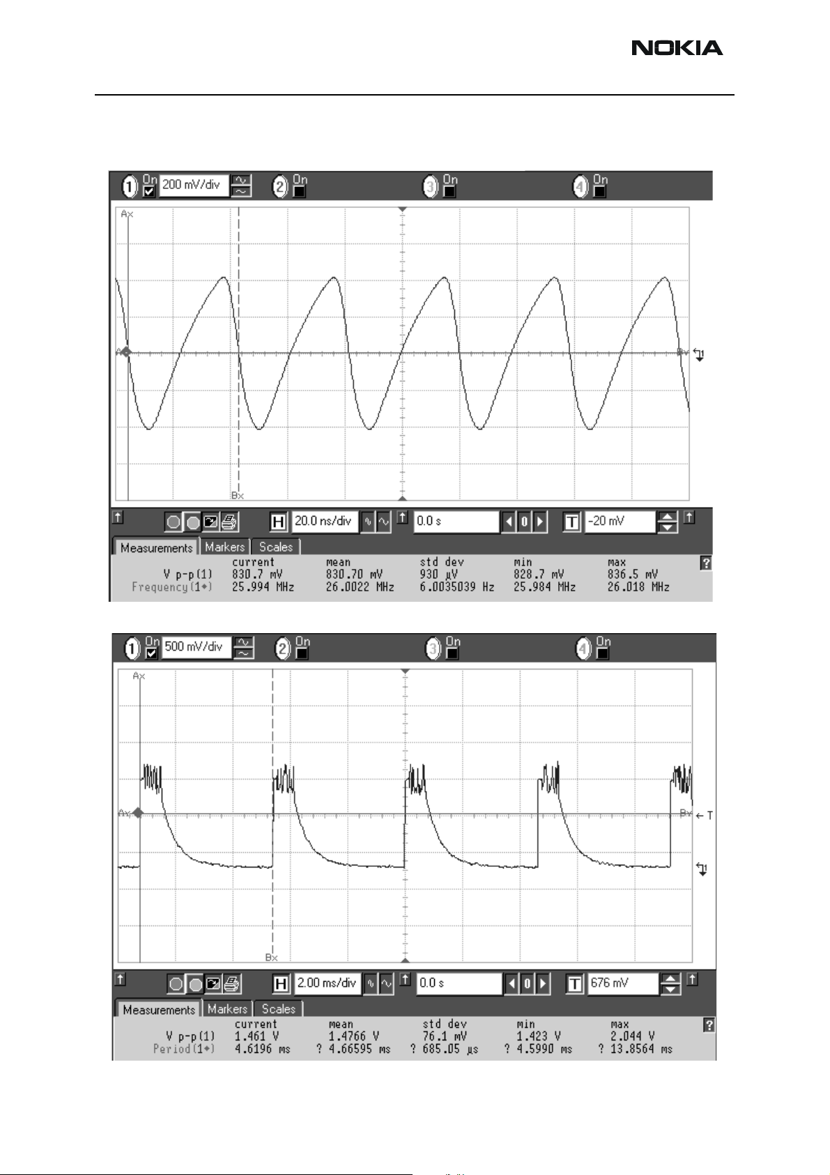
Figure 5: TP20: 26 MHz VCTCXO output signal
Figure 6: TP21: TX I/Q signal
Page 18 Nokia Corporation Issue 1 04/03
Page 19
NSB-9
CCS Technical Documentation Troubleshooting Instructions
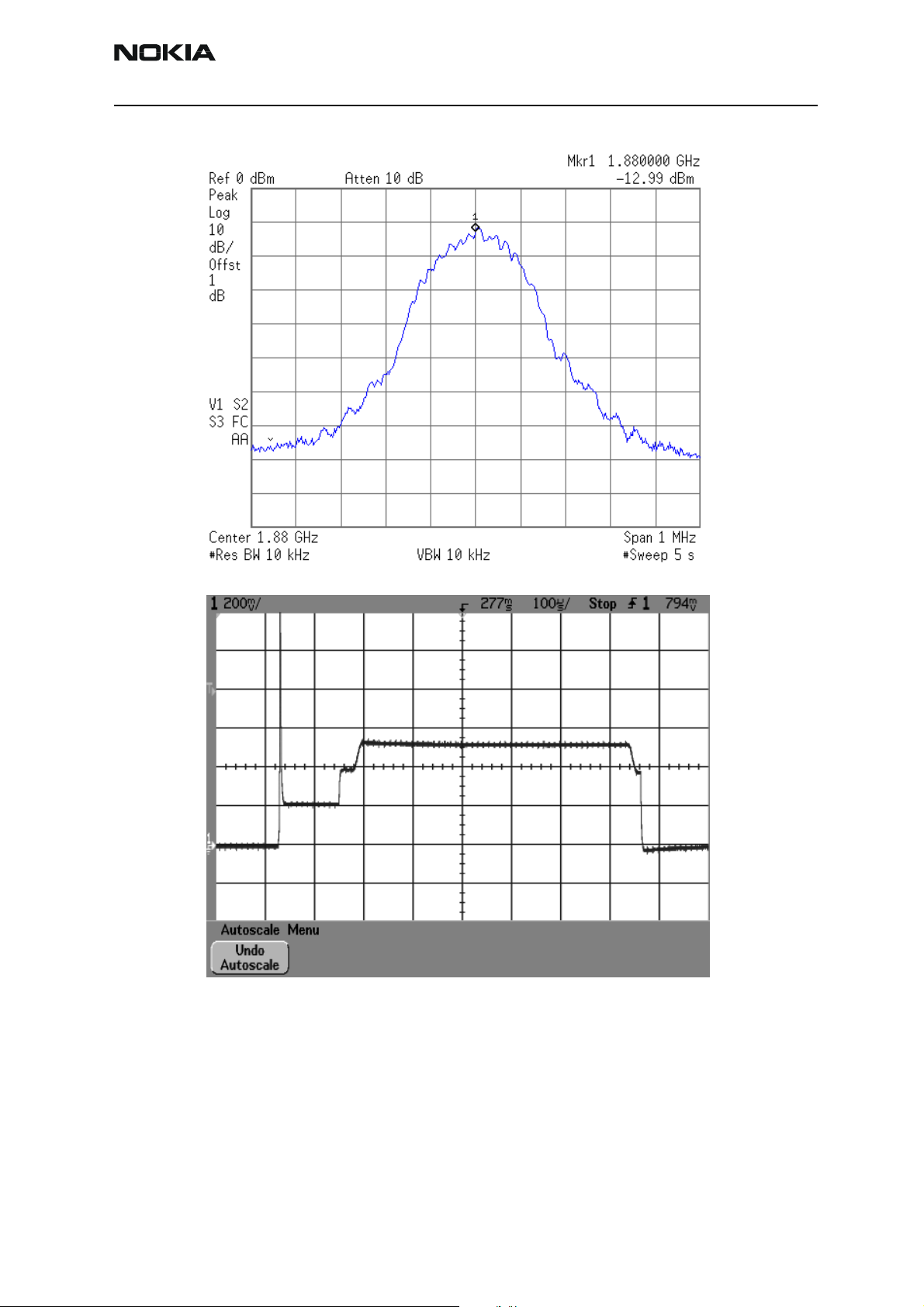
Figure 7: TP22: TX1900 modulator output signal
Figure 8: TP23: TXC signal from UEM ASIC
Issue 1 04/03 Nokia Corporation Page 19
Page 20
NSB-9
Troubleshooting Instructions CCS Technical Documentation
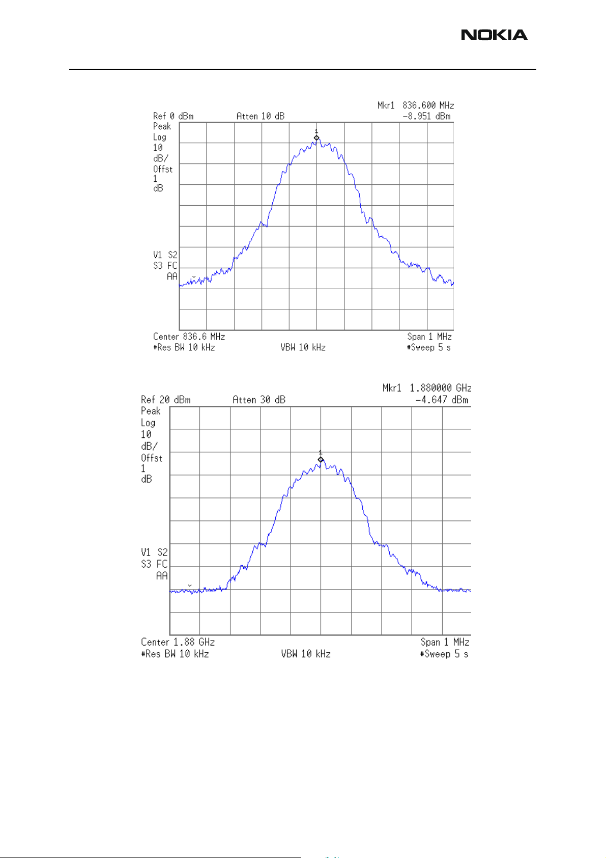
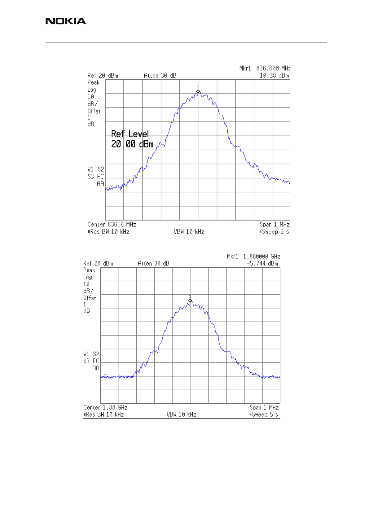
Figure 9: TP24: TX850 modulator output signal
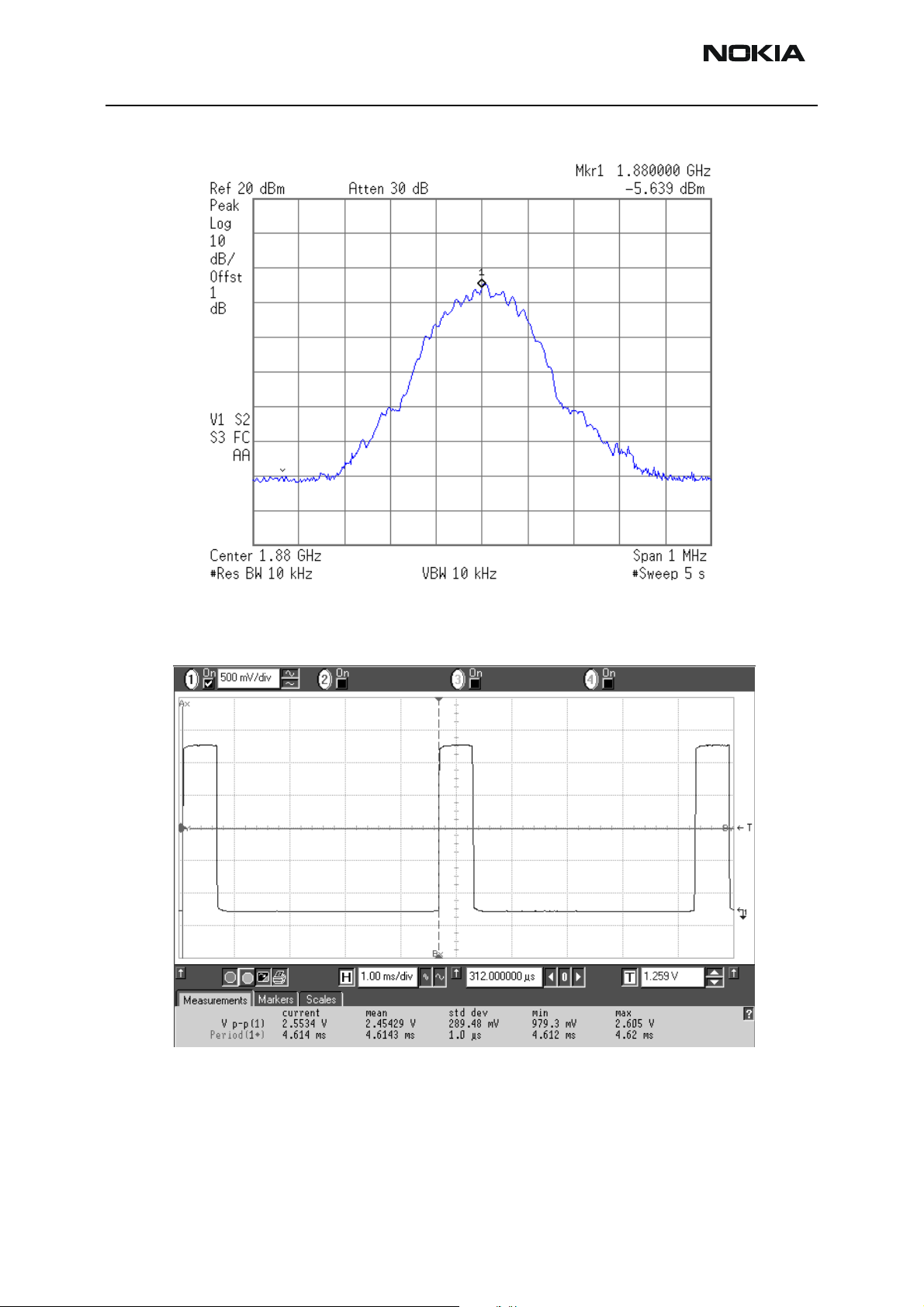
Figure 10: TP25: TX1900 PA output signal
Page 20 Nokia Corporation Issue 1 04/03
Page 21
NSB-9
CCS Technical Documentation Troubleshooting Instructions
Figure 11: TP 26: TX1900 PA power control signal
Figure 12: TP27: TX850 PA power control signal
Issue 1 04/03 Nokia Corporation Page 21
Page 22
NSB-9
Troubleshooting Instructions CCS Technical Documentation
Figure 13: TP 28: TX1900 signal at coupler output
Figure 14: TP29: Antenna switch control signal in TX1900 mode
Page 22 Nokia Corporation Issue 1 04/03
Page 23
NSB-9
CCS Technical Documentation Troubleshooting Instructions
Figure 15: TP30: TX850 signal at antenna pad
Figure 16: TP30: TX1900 signal at antenna pad
Issue 1 04/03 Nokia Corporation Page 23
Page 24
NSB-9
Troubleshooting Instructions CCS Technical Documentation
Figure 17: TP31: RX1900 signal at antenna switch output
Figure 18: TP32: RX1900 signal at dual SAW filter output
Page 24 Nokia Corporation Issue 1 04/03
Page 25

NSB-9
CCS Technical Documentation Troubleshooting Instructions
Figure 19: TP33: RX1900 signal at LNA output
Figure 20: TP34, TP35: RX1900 LNA control signals (Burst mode)
Issue 1 04/03 Nokia Corporation Page 25
Page 26

NSB-9
Troubleshooting Instructions CCS Technical Documentation
Figure 21: TP36: RX1900 signal at 2nd band filter output
Figure 22: TP37: RX IQ signal (Burst Mode)
Page 26 Nokia Corporation Issue 1 04/03
Page 27

NSB-9
CCS Technical Documentation Troubleshooting Instructions
Figure 23: TP37: RX IQ signal (GSM850, Continuous Mode, Signal level -90 dBm)
Figure 24: TP37: RX IQ signal (GSM1900, Continuous Mode, Signal level -90 dBm)
Issue 1 04/03 Nokia Corporation Page 27
Page 28

NSB-9
Troubleshooting Instructions CCS Technical Documentation
Figure 25: TP40: SHF VCO output signal in TX850 mode
Figure 26: TP40: SHF VCO output signal in TX1900 mode
Page 28 Nokia Corporation Issue 1 04/03
Page 29

NSB-9
CCS Technical Documentation Troubleshooting Instructions
Figure 27: TP40: SHF VCO output signal in RX850 mode
Figure 28: TP40: SHF VCO output signal in RX1900 mode
Issue 1 04/03 Nokia Corporation Page 29
Page 30

NSB-9
Troubleshooting Instructions CCS Technical Documentation
Figure 29: TP51,52,53: SDATA, SCLK and SLE signals in GSM850/1900 mode
Figure 30: TP60: TX850 PA Output Signal
Page 30 Nokia Corporation Issue 1 04/03
Page 31

NSB-9
CCS Technical Documentation Troubleshooting Instructions
Figure 31: TP61: TX850 signal at coupler output
Figure 32: TP62: Antenna switch control signal in TX850 mode
Issue 1 04/03 Nokia Corporation Page 31
Page 32

NSB-9
Troubleshooting Instructions CCS Technical Documentation
Figure 33: TP 63: RX850 signal at antenna switch output
Figure 34: TP 64: RX850 signal at dual SAW filter output
Page 32 Nokia Corporation Issue 1 04/03
Page 33

NSB-9
CCS Technical Documentation Troubleshooting Instructions
TP 65, 67: RX850 LNA control signals (Burst mode)
Figure 35: TP 66: RX850 signal at LNA output
Issue 1 04/03 Nokia Corporation Page 33
Page 34

NSB-9
Troubleshooting Instructions CCS Technical Documentation
Figure 36: TP68: RX850 signal at 2nd band filter output
Page 34 Nokia Corporation Issue 1 04/03
Page 35

NSB-9
CCS Technical Documentation Troubleshooting Instructions
FM Radio Troubleshooting
Introduction
This document describes the methods of FM radio troubleshooting for Iris NSB-9 transceiver.
EQUIPMENT NEEDED
NSB-9 module jig MJS-48, power and DAU-9S cables
DC power supply 3.9 VDC >3A
Digital multimeter (DMM)
Audio Analyzer
Oscilloscope with 1 MHz 1:1 probe
PC with Phoenix software
Headset (HDB-4 or HDS-3)
Issue 1 04/03 Nokia Corporation Page 35
Page 36

NSB-9
Troubleshooting Instructions CCS Technical Documentation
FM RADIO SCHEMATICS
Figure 37: Input signal connection to antenna (headset cable)
Figure 38: Input signal single to differential conversion
Page 36 Nokia Corporation Issue 1 04/03
Page 37

NSB-9
CCS Technical Documentation Troubleshooting Instructions
Figure 39: VCO components
Figure 40: Connection to UPP
Issue 1 04/03 Nokia Corporation Page 37
Page 38

NSB-9
Troubleshooting Instructions CCS Technical Documentation
Figure 41: Audio signal output
Page 38 Nokia Corporation Issue 1 04/03
Page 39

NSB-9
CCS Technical Documentation Troubleshooting Instructions
FM Radio layout
Figure 42: Components
Figure 43: Components on PWB
Note! Components L105, L106, L107, L108, L109, C108, C109, C110, C111, R164, R165, R166, R167,
R170 and R171 are not shown in the picture. Components are placed near audio amplifier N150.
Issue 1 04/03 Nokia Corporation Page 39
Page 40

NSB-9
p
Troubleshooting Instructions CCS Technical Documentation
Figure 44: FM radio testpoints
AUDIO AMPLIFIER
HSEAR R
VFLASH2
HSEAR L
J359, FMCLK
J356, FMCTRLDA
J358, FMWREN
J357, FMCTRLCLK
FM RADIO R FM RADIO L
J104, HSEAR P
J105, FM RADIO
ANTENNA INPUT
J103, HSEAR R N
Page 40 Nokia Corporation Issue 1 04/03
Page 41

NSB-9
CCS Technical Documentation Troubleshooting Instructions
Figure 45: FM radio fault finding chart
Turn on FM radio in local
mode. Does the radio start?
9
Apply RF input signal
= 98 MHz
f
0
∆f= 75 kHz
f
= 1 kHz
m
level= -90 dBm
Set radio channel to
98 MHz
Set audio volume to
maximum (100%)
9
Check audio signal at audio
amplifier N150 input (C170
and C171).
Is the frequency 1 kHz and
amplitude 0.5…0.8 Vpp?
Check components around
8
FM radio serial bus and
clock signal (C374, C375,
R357 and R361).
Check 32 kHz clock signal
at J359. Does the radio
start now?
9
9
Replace N356.
Does the radio start
now?
8
Check supply voltages at
TEA5767 (N356) pins 7 and
34 (2.78 VDC).
Does the radio start now?
9
9
Check N356 soldering
8
(all pins).
Does the radio start
now?
8
8
Baseband digital
failure (UPP)
Set radio channel and RF
generator to 88.1 Mhz. Re-
9 Audio amplifier failure
check audio signal level
(0.5…0.8 Vpp at C170 and
C171). Re-check also in
107.9 MHz.
9
(N150)
8
Check RF input
components (C108…C111,
L109, C367, C378, 379 and
L358).
Re-check audio signal at
C170 and C171. Is the
frequency 1 kHz and
amplitude 0.5…0.8 Vpp?
8
9
8
Check VCO components
(V356,V357, L356, L357,
C357, C358, C362, R359,
(0.5…0.8 Vpp at C170 and
R360).
Re-check audio signal
C171) in 88.1 MHz and
107.9 MHz.
9
Replace TEA5767
(N356)
Re-check audio signal
(0.5…0.8 Vpp at C170
and C171) in 88.1
MHz and 107.9 MHz.
8
8
Replace transceiver
NSB-9
9
8
Check audio amplifier
output (R164…R167,
L105…L108).
Check audio signal at J103
and J104. Is the frequency
1 kHz and amplitude
0.015…0.3 Vpp?
9
FM radio is OK
Issue 1 04/03 Nokia Corporation Page 41
Page 42

NSB-9
Troubleshooting Instructions CCS Technical Documentation
REFERENCE MEASUREMENT RESULTS
Figure 46: Audio output signal
Signal 1: Audio output signal at PWB test points J103 and J104 (FM test signal, audio
volume 100%)
Signal 2: Audio output at FM radio pins 22 and 23 (same signal as in C170 and C171)
Page 42 Nokia Corporation Issue 1 04/03
Page 43

NSB-9
CCS Technical Documentation Troubleshooting Instructions
Figure 47: Reference clock signal from UPP
FM radio clock at test point J359 (32 kHz clock signal when radio is turned on)
Figure 48: RF input signal
15:51:49 03 JUL 2002
#AT 0 dBREF -20.0 dBm
PEAK
LOG
10
dB/
WA SB
CORR
SC FS
CENTER 98.0000 MHz SPAN 300.0 kHz
#RES BW 10 kHz VBW 10 kHz #SWP 1.00 sec
MKR 97.9280 MHz
-71.03 dBm
SWEEP
CONT SGL
FREE RUN
VIDEO
LINE
EXTERNAL
SYNC CRD
TV TRIG
FM modulated test signal at FM radio ASIC pin 37, at the other end of L358
Issue 1 04/03 Nokia Corporation Page 43
Page 44

NSB-9
Troubleshooting Instructions CCS Technical Documentation
Figure 49: VCO signal
10:46:24 03 JUL 2002
#AT 10 dBREF .0 dBm
PEAK
LOG
10
dB/
WA SB
CORR
SC FS
CENTER 196.450 MHz SPAN 1.000 MHz
#RES BW 10 kHz #VBW 10 kHz #SWP 20.0 msec
MKR
196.440 MHz
-9.40 dB
MEAS UNCAL
SWEEP
CONT SGL
FREE RUN
VIDEO
LINE
EXTERNAL
SYNC CRD
TV TRIG
VCO frequency at FM radio pins 3 and 4, at the other ends of V356 and V357
Page 44 Nokia Corporation Issue 1 04/03
Page 45

NSB-9
CCS Technical Documentation Troubleshooting Instructions
Baseband Troubleshooting
PWB Test points
Figure 50: Flash programming testpoints
J101, BSI
J102, BTEMP VBAT
FBUS RX
FBUS TX
GND
MBUS
VPP
J1, RESET
J2, RFBUSDA
J3, RFBUSCLK
J4, RFBUSEN1
Issue 1 04/03 Nokia Corporation Page 45
Page 46

NSB-9
Troubleshooting Instructions CCS Technical Documentation
J410, MBUSRX
J412, FBUSRX
J100, VBAT
J409, MBUSTX
J404, SLEEPCLK
J411, FBUSTX
J415, DBUSEN1X
VCORE
VFLASH2
J402, PURX
J403, SLEEPX
VANA
Figure 51: Baseband testpoints
VBATT6
VFLASH1 VIO
VBATT4
VBATT2
VBATT3
VBATT1
VBATT5
J405, UEMINT
J414, DBUSDA
J413, DBUSCLK
J419, FLSCLK
J418, FLS2CSX
J420, FLSCSX
J416, EXTWRX
J417, EXTRDX
Page 46 Nokia Corporation Issue 1 04/03
Page 47

NSB-9
CCS Technical Documentation Troubleshooting Instructions
J404, SLEEPCLK
J407, CBUSDA
J402, PURX
Figure 52: SIM testpoints
VIO VSIM
J408, CBUSENX
J406, CBUSCLK
SIMRST
SIMCLK
VSIM
SIMRST
SIMIODA
Issue 1 04/03 Nokia Corporation Page 47
Page 48

NSB-9
Troubleshooting Instructions CCS Technical Documentation
Figure 53: Miscellanous testpoints
EARP EARN
J306 J302
FLIP CLOCK FLIP VBAT FLIP GND FLIP DATA
J305 J301
J304 J308
J303 J307
J153, CLK
J152, ENB
N301 HALL-SENSOR
J154, DATA
Audio amplifier
control lines, some
are placed under
dome sheet
Page 48 Nokia Corporation Issue 1 04/03
Page 49

NSB-9
CCS Technical Documentation Troubleshooting Instructions
J150, IHF -
J151, IHF +
V319 UPPER FLIP VBAT SWITCH
V319 LOWER FLIP VBAT SWITCH
VIBRA VBAT
UEM VIBRA
J331, HALL SENSOR OUTPUT
J106, MICN
J107, MICP
X102
PIN 1
GND VCHAR
Issue 1 04/03 Nokia Corporation Page 49
Page 50

NSB-9
Troubleshooting Instructions CCS Technical Documentation
Signal Name Function Test Point Signal Characteristics Notes
FBUS_TX Flash programming data and phone
FBUS_RX Flash programming data and phone
MBUS Flash programming clock and phone
BSI Flash programming startup
VPP Flash programming voltage PRODTP6 1.8V, up to12V during
VR1A Power supply for Hagar PLL charge
VR2 Power supply for TX modulator C706 2.8 V
VR3 Power supply for VCTCXO C662 2.8 V Controlled by SLEEPX signal
VR4 Power supply for Hagar C601 2.8 V
VR5 Power supply for Hagar C603 2.8 V
VR6 Power supply for Hagar C605 2.8 V
VR7 Power supply for VCO R652 2.8 V
Signal Name Function Test Point Signal Characteristics Notes
VSIM Power supply for SIM card C390/conn. 1.8 or 3.0V Level depend on SIM card type
SIMRST SIM reset C387/conn. digital signal Level depend on SIM card type
SIMIODAO SIM data C386/conn. digital signal Level depend on SIM card type
SIMCLKO SIM clock C388/conn. 3.25 MHz digital clock
SLEEPX Sleep mode control J403 1.8-0V, digital signal
PURX Power up reset J402 1.8-0V, digital signal
SLEEPCLK Sleep clock J404 1.8-0V, 32 kHz digital
Signal Name Function Test Point Signal Characteristics Notes
VBATTO_1 Power supply for VANA,VR3,VR4
VBATTO_2 Power supply for
VBATTO_3 Power supply for VCORE regulator C262 = VBAT
VBATTO_4 Power supply for VR1A,VR1B and
VBATTO_5 Power supply for VR5 and VR6
VBATTO_6 Power supply for VIO regulator C265 = VBAT
RFCLK System clock for baseband C420 13 MHz analog signal Requirement > 0.3 Vpp
RF_BUSDA Hagar control serial data J2 0 -1.8V, digital signal
RF_BUSCLK Hagar control serial clock J3 0 -1.8V, 13 MHz digital
Signal Name Function Test Point Signal Characteristics Notes
CBUSCLK Serial clock J406 1.8-0V, 1MHz digital clock
CBUSDA Serial data input/output J407 1.8-0V, digital signal Controlled by MCU
control
control
control
signal,battery size indicator, local
mode switch, SIM card detection
pump
and VR7 regulators
VFLASH1,VFLASH2 and VSIM
regulators
VR2 regulators
regulators
PRODTP2 2.8-0V, digital signal From phone to prommer or PC
PRODTP3 2.8-0V, digital signal From prommer or PC to phone
PRODTP7 2.8-0V, digital signal,
Battery
connector
and J101
C600 4.75 V
C260 = VBAT
C261 = VBAT
C264 = VBAT
C263 = VBAT
clocks up to 6.5MHz
2.8-0V, analog ADconverter and digital signal
flash programming
signal
clock signal
clock signal
signal
Bidirectional phone control
2.8V pulse when flashing starts, approx. 1.0V
in normal mode and 0V in local mode
Internal programming voltage 1.8V , external
12V
Level depend on SIM card type
Controlled by MCU
Page 50 Nokia Corporation Issue 1 04/03
Page 51

NSB-9
CCS Technical Documentation Troubleshooting Instructions
CBUSENX CBUS selection and enable J408 1.8-0V, digital signal
VIO Power supply for LCD, UPP and flash
VFLASH1 Power supply for LCD, IR and flash
VANA Power supply for UEM (AD, RF and
VCORE Power supply for UPP C208 1.0-1.8V programmable 1.8 V used in NHM-4, initial value is 1.5V
DLIGHT DC/DC converter control Converter
Signal Name Function Test Point Signal Characteristics Notes
RESET Hagar reset J1 0 -1.8V, digital signal
RF_BUSEN1 Hagar chip select and latch enable J4 1.8-0V, digital signal
XRES LCD reset X300/2 1.8-0V, digital signal
SI LCD serial data input X300/3 0 -1.8V, digital signal
SCI LCD serial clock input X300/6 0 -1.8V, 3.25 MHz digital
XCS LCD chip select X300/5 1.8-0V, digital signal
EXTRDX Flash memory read enable J417 1.8-0V, digital signal
FLSCSX Flash memory chip select J420 1.8-0V, digital signal
FLSCLK Flash memory clock in burst mode J419
EXTWRX Flash memory write enable J416 1.8-0V, digital signal
Signal Name Function Test Point Signal Characteristics Notes
VBAT Battery voltage for UEM, power
memory
memory
audio codecs)
amplifier, DC/DC converter, IR,
C207 1.8V
C205 2.8V
C206 2.8V
pin8
Battery
connector
VBAT
∼∼∼∼
clock signal
0 -1.8V,
35 MHz digital
∼∼∼∼
clock signal
3.6V 3.1V – 4.2V
Controlled by MCU
Burst mode only when read
audio amp, keyboard leds and vibra
BTEMP Battery temperature, test mode
switch
Battery
connector
and J102
FBUSRX FBUS from UEM to UPP J412 0 -1.8V, digital signal
FBUSTX FBUS from UPP to UEM J411 1.8-0V, digital signal
UEMINT Interrupt request for UPP J405 0 -1.8V, digital signal
DBUSDA DBUS clock J414 0 -1.8V, digital signal Controlled by DSP
DBUSCLK DBUS data input/output J413 0 -1.8V, 13 MHz digital
Controlled by DSP
clock signal
DBUSEN1X DBUS selection and enable J415 1.8-0V, digital signal Controlled by DSP
MBUSRX MBUS from UEM to UPP J410 1.8-0V, digital signal
MBUSTX MBUS from UPP to UEM J409 1.8-0V, digital signal
Issue 1 04/03 Nokia Corporation Page 51
Page 52

NSB-9
Troubleshooting Instructions CCS Technical Documentation
Troubleshooting steps
The following hints help to find the problem if the circuitry seems to be faulty. The
instructions are divided into following sections:
1. Phone is dead
2. Flash faults
3. Phone is jammed
4. Charging fault
5. Sim card fault
6. Audio faults
7. Display faults
8. Keypad fault
9. FM-radio faults
The first thing to do is to carry out a thorough visual check of the module. Ensure in particular that:
1. there is no any mechanical damages
2. soldered joints are OK
Page 52 Nokia Corporation Issue 1 04/03
Page 53

NSB-9
No No No N
CCS Technical Documentation Troubleshooting Instructions
Main troubleshooting tree
TOP
Phone is
totally dead
o
Flash
programming
doesn´t work
Phone doesn´t
start up or the
phone is
jammed
Yes
Yes
Yes
Phone
is dead
Flash
faults
Phone
is
jammed
Charging
doesn´t work
TOP
2
Yes
Charging
fault
Issue 1 04/03 Nokia Corporation Page 53
Page 54

NSB-9
No N
No N
Troubleshooting Instructions CCS Technical Documentation
TOP
2
Phone doesn´t
read SIM card
o
Audio faults
Display or
LED´s doesn´t
work
Yes
Yes
Yes
SIM
card
fault
Audio
faults
Display
faults
Keypad
doesn´t work
Yes
Keypad
faults
o
FM Radio
doesn´t work
Yes
FM
Radio
faults
No
END
Page 54 Nokia Corporation Issue 1 04/03
Page 55

NSB-9
j
NoN
N
NoN
N
CCS Technical Documentation Troubleshooting Instructions
Phone is dead
Phone
is
dead
Phone current is
0mA?
o
Phone current is
< 26mA
Phone current is
26-30mA
Yes
Yes
Yes
Check X100 solder.
Check L260 – L265 and
C260 – C265.
Check all VBAT lines.
Is phone flash
programing
OK?
o
Yes
o
Phone
is
ammed
Flash
fauItIs
Is phone in
LOCAL mode
Yes
Retest
Check BSI line
X100, C114,
R202, C240,
R206 Are they
OK?
o
Yes
Change UEM
Change defect part
Issue 1 04/03 Nokia Corporation Page 55
Page 56

NSB-9
No No N
N
Troubleshooting Instructions CCS Technical Documentation
Flash faults
Flash
faults
The phone does
not set FBUSTX
line high after
the startup.
o
The phone does
not set FBUSTX
line low after the
line has been
high.
Yes
Yes
Measure BSI
pulse during
Flash
programming.
Is it OK ?
Yes
Measure FBUSTX
line during Flash
programming from
testpoint J411. Is
it ~1.8V
Yes
Check BSI
line. X100,
C114, C240,
R202, R206
Check R109
if OK,
Change
UEM
Change
UPP
Change
UPP
o
Flash
faults
page 2
Page 56 Nokia Corporation Issue 1 04/03
Page 57

NSB-9
No No N
CCS Technical Documentation Troubleshooting Instructions
Flash
faults
page 2
Wrong
manufactor ID
and Device ID
o
Is the phone
totally dead?
Phone doesn´t
start up or the
phone is
jammed?
Yes
Yes
Yes
Change
FLASH
Phone
is dead
Phone
is
jammed
Retest
Issue 1 04/03 Nokia Corporation Page 57
Page 58

NSB-9
j
No N
No No No No N
Troubleshooting Instructions CCS Technical Documentation
Phone is jammed
Phone
is
ammed
Measure VIO,
VCORE, FLASH1,
VANA, VR3 voltages.
Are they OK?
Yes
Measure 32.6kHz
Sleep CLK from
testpoint J404. Is it
OK?
Yes
Measure 13MHz
RFClk from R420. Is it
OK?
Yes
Check VBATT 1-6
VIO, VCORE,
FLASH1, VANA,
VR3 lines. Are they
OK?
Yes
Measure 32.6kHz
Sleep Clk from
B200. Is it OK?
Yes
o
Measure 26MHz
RFClk from C660.
Is it OK?
Yes
Check L260-L265
C260-C265
BSI/BTEMP lines and
VBATT lines
Check BSI/BTEMP
lines. If OK and UEM
regulators are not
working. Change
UEM
Check B200, C209,
Check R661, C661,
R660, C660 and
VR3 line. If OK,
change G660.
Check R420, C420. If
OK change N600
C210
Change UEM
Measure PURX signal
from testpoint J402.Is it
high (~1.8V)?
Yes
Jammed
page2
o
Change UEM
Page 58 Nokia Corporation Issue 1 04/03
Page 59

NSB-9
N
N
N
N
OK?
CCS Technical Documentation Troubleshooting Instructions
Jammed
page2
Phone shutdown
after 30s
o
Measure DBUSClk
1 Mhz signal from
testpoint J413. Is it
Yes
Read phone info.
Is it OK?
Yes
Yes
No
Measure watchdog
signal CBUSDA
from testpoint J407
Is it OK?
o
Measure FBUSRX
signal during
phone info read
from testpoint 412.
Is it OK?
Yes
o
Yes
Change UPP
Change UEM
Retest
Measure FBUSTX
signal during phone
info read from
testpoint J411. Is it
Yes
o
Change UPP
Change UEM
Issue 1 04/03 Nokia Corporation Page 59
Page 60

NSB-9
N
No No N
N
N
Troubleshooting Instructions CCS Technical Documentation
Charging fault
Charging
fault
Connect
ACP
(
charger
-7)
Battery bar doesn´t
work (scroll)
Yes
Measure voltage
over V100 Is it > 3.0
Vdc?
Yes
Read BTEMP value.
(Compare it to
ambient temperature)
Is it ~25 C (0319)?
Retest
o
Check X101,
X102, F100, L100,
V100, C100, C101
and charger line.
Check X100,
C114, R202,
C220, R207 and
line. Are they OK?
Yes
Change defected
part
Re-calibrate
BTEMP and
retest.
Yes
Measure charger
current through F100.
Is it ~350...390mA
with ACP-7?
-
Yes
Retest
o
o
Check R200. Is
it OK?
Yes
Change defect ,
re-calibrate and
retest
Change UEM
o
Change defected part,
recalibrate charge
current/voltage.
Page 60 Nokia Corporation Issue 1 04/03
Page 61

NSB-9
No No No No
CCS Technical Documentation Troubleshooting Instructions
SIM card fault
SIM
card
Insert SIM or
Card rejected
fault
Yes
Check X386. Is
it OK?
Yes
Try to set
phone in local
mode. Is it OK?
Yes
Measure VSIM
voltage at
X386. Is it
~3.0V
Change defected
part
Check BSI-line
including X100,
C100, C240, R202
and R206. If OK,
change UEM
Check VSIM line
X386, C390, C203.
If OK, change
R388. If still fail,
change UEM.
Yes
Retest
Check SIM
power-up
sequence. Is it
OK?
Yes
Check SIM lines
X386. If OK,
change R388. If still
fail, change UEM.
Change UPP
Issue 1 04/03 Nokia Corporation Page 61
Page 62

NSB-9
No No N
N
Troubleshooting Instructions CCS Technical Documentation
Audio faults
Audio
faults 1
Is the earpiece
working ?
Yes
Try to change the
earpiece. Is it
working now?
o
Set phone to LOCAL mode. Set routing
EXT IN, HP OUT by using phoenix
“Audio Routing and Test Signals” test
Measure DC offset
voltage from earpiece
pads (against GND).
Is it ~1.36V ?
Yes
Measure MICB2 voltage
from XMICP (X102 /
pin10). Is it ~1.9V with
headset?
Yes
Check L150, C180,
C181, R152, R153
and line. If OK ->
change UEM
Check L103, R161,
o
C163, C162, R156,
R157, C158, C152,
C159 and line. If OK
-> change UEM
Retest
Yes
Audio
faults 2
Earpiece 2
Page 62 Nokia Corporation Issue 1 04/03
Page 63

NSB-9
N
CCS Technical Documentation Troubleshooting Instructions
Earpiece
2
Connect external 1kHz (sine
200mVpp) audio signal in XMICP
line and ground line to XMICN
line.
Measure
differential sine
signal from
earpiece pads. Is
it ~190mVpp?
Yes
Retest
No
Measure signal
from C152,
(XMICP). Is it
~110mVpp?
o
Check L150,
Yes
Check L103, L104, R161,
C163, C162, R156, R157,
C158, C152, C159 and
corresponding componenets
from XMICN line.
R152, R153,
C180, C181 If
still fail, change
UEM
Issue 1 04/03 Nokia Corporation Page 63
Page 64

NSB-9
N
N
N
N
N
N
Troubleshooting Instructions CCS Technical Documentation
Audio
faults 2
Is the IHF
speaker
working?
Yes
Change
defected part
and retest
o
o
Set phone in LOCAL mode. Use
Phoenix “Audio Routing and Test
Signals” test. Set output path as IHF
Measure DC
offset voltage
from speaker
pads (J150 / J151
to GND). Is it
~1.9V?
Check IHF
speaker
connections.
Is it OK?
speaker
(1
Yes
o
Try to change
IHF speaker.
Is it working
now?
Check L151,
L152, R162,
C172 and
line. OK?
Yes
Yes
Retest
o
o
Change defected
parts
Yes
Check data
communication of
audio amp. control
lines J152, J153,
J154. Is it OK?
Audio
faults 3
IHF 2
Yes
Change N150
1) If not working set first “All outputs off” and after that “IHF speaker”
Check lines if OK
o
change UPP.
If NOK change
Page 64 Nokia Corporation Issue 1 04/03
Page 65

NSB-9
N
N
CCS Technical Documentation Troubleshooting Instructions
IHF 2
Use Phoenix “Audio Routing and
Test Signals” test. Use internal
sine wave generator and set
signal frequency to 1kHz and
peak level to 4000 Hex
Measure
differential sine
signal from IHF
speaker pads
J150, J151. Is it
~810mVpp?
o
Check C174,
C179, C178, R163
and XAUDIO(7)
line. Are they OK?
o
Change defect
part and retest
Yes
Retest
Yes
Change UEM
and retest
Issue 1 04/03 Nokia Corporation Page 65
Page 66

NSB-9
N
N
N
N
N
Troubleshooting Instructions CCS Technical Documentation
Audio
faults 3
Is the
External
Audio out
working?
Yes
Change defected
part and retest
o
o
Set phone in LOCAL mode. Use Phoenix
“Audio Routing and Test Signals” test. Set
output path as HP speaker. Insert headset to
Measure DC offset
voltage from
HSEAR P&N and
HSEAR R P&N
lines. Is it ~2.0V?
Check system
connector and
soldering. Are
they OK?
route audio to HSEAR
(2
o
Check X102
L103 - L106, C108 C111, C115 - C118,
R111 - R114, C165,
C167, R164 - R167
and line. OK?
o
Change defected
parts
Audio
faults 4
Yes
communication of
audio pa control lines
J152, J153, J154. Is
Ext. audio
out 2
Yes
Check data
it OK?
Yes
Change N150
Check lines if OK
change UPP.
o
If NOK change
radio module
TB9
2) If not working set first “All outputs off” and after that “HP speaker”, after that insert headset again
Page 66 Nokia Corporation Issue 1 04/03
Page 67

NSB-9
N
N
CCS Technical Documentation Troubleshooting Instructions
Ext.
audio out
2
Yes
Use Phoenix “Audio Routing and
Test Signals” Test. Use internal
sine wave generator and set
signal frequency to 1kHz and
peak level to 4000 Hex
Measure differential
sine signal from
HSEAR P&N and
HSEAR R P&N
speaker pads. Is it
~60mVpp?
Yes
Retest
o
Check C174,
C169 and
XAUDIO(7) line.
Are they OK?
o
Change defect
part and retest
Yes
Change UEM
and retest
Issue 1 04/03 Nokia Corporation Page 67
Page 68

NSB-9
No N
N
No N
N
Troubleshooting Instructions CCS Technical Documentation
Audio
faults 4
Is internal
microphone
working ?
Yes
Check microphone
connector. Is it OK
o
Try to change
microphone. Is it
working now?
o
Set phone in LOCAL mode. Use Phoenix
“Audio Routing and Test Signals” Test. Set
Connect external 1kHz (sine 30mVpp)
audio signal in MICP line and ground line
routing HP in Ext out
Yes
Measure MICB1 voltage
from MICP (J107). Is it
~2.1V ?
Yes
to MICN line
(3
Yes
Change defect part and
Check L110, C153,
o
R155, C154 and
line. If OK -> change
retest
Retest
UEM
Audio
faults 5
Measure sine signal
from HSEAR and
HSEAR R lines. Is it
~160mVpp with
headset?
Yes
Retest
o
Check R154, C150
and line. If OK ->
change UEM
3) If you don’t get such a small signal out from signal generator, use resistor network to attenuate
Page 68 Nokia Corporation Issue 1 04/03
Page 69

NSB-9
No N
N
N
N
N
CCS Technical Documentation Troubleshooting Instructions
Audio
faults 5
Is external
microphone
working ?
Yes
o
Set phone in LOCAL mode. Use Phoenix
“Audio Routing and Test Signals” Test. Set
Connect external 1kHz (sine 200mVpp)
audio signal in XMICP line and ground line
Check if external
audio device is OK?
Yes
Check system
connector X102. Is
it OK ?
Yes
routing Ext in HP out
Yes
Measure MICB2 voltage
from XMICP (X102 / pin
10). Is it ~2.0V with
headset?
Yes
to XMICN line.
(4
o
o
C162, R157, C158 and line. If
Retest with
undamaged ext. audio
device.
Change defect part and
retest
Check L103, R161, C163,
OK -> change UEM
Check C159 If OK, change
UEM
Yes
Measure sine signal
from EARP and EARN
lines. Is it ~190mVpp?
END
Yes
Retest
4) If not working set “Loops Off” and after that “Ext in HP out” again
o
Check L103, R161, C163, C162, R156,
R157, C158, C152, C159 and also
corresponding componenets from
XMICN line line. Change defect part.
Measure signal
from C152. Is it
~110mVpp?
o
Issue 1 04/03 Nokia Corporation Page 69
Page 70

NSB-9
N
No No No N
Troubleshooting Instructions CCS Technical Documentation
Display faults
Display
faults
Set phone in LOCAL mode.
Start Display test with Phoenix
Try to change
display module.
Is it working now?
Yes
Retest
Are the display
module LED´s
turned ON?
Yes
Display
faults 2
o
Measure signal from
X300 pin 10.
Is it 10 – 14V?
Check R306. If OK
measure VBAT from
N300 pin 1.
Is it OK?
Yes
Check LED driver
control signal from
N300 pin 8.
Is it high?
Yes
Check
X300
Yes
Check X300
Check C300 and
VBAT line
o
Check N300, C301, V300,
L300, C302, R318 and
change defect componenet
Check control
signal line. If OK
change UEM.
Page 70 Nokia Corporation Issue 1 04/03
Page 71

NSB-9
N
N
N
N
CCS Technical Documentation Troubleshooting Instructions
Display
faults 2
Does the display
start?
Yes
o
Measure
VDD (2.78V) and
VDDI (1.8V).
Are they OK?
Yes
Try to chance the
display module. Is it
working now?
o
Check X300
o
Yes
Retest
Check C305, C306
and lines. If OK,
change UEM.
Measure XRES,
XCS, SI. Are
voltage levels
~1.8V?
o
Check X300 and
lines.
If OK, change UPP.
Yes
END
Issue 1 04/03 Nokia Corporation Page 71
Page 72

NSB-9
No No No
N
Troubleshooting Instructions CCS Technical Documentation
Keypad faults
Keypad
faults
Is the power
key working?
Yes
Measure
voltage from
S336 when
key is pressed.
Is it high?
Measure voltage
from S336. Is it
high?
Yes
Check S336.
Yes
Is it OK?
Check R317,
C311, S336 and
line.
If OK change
UEM.
Yes
Phone
is dead
o
Change S336
Keypad
faults 2
Phone
is
jammed
Page 72 Nokia Corporation Issue 1 04/03
Page 73

NSB-9
N
N
No No N
N
CCS Technical Documentation Troubleshooting Instructions
Keypad
faults 2
Are flip T9
keys
working?
o
Check flip poco pins,
engine contact pads.
and spring contacts
between A-cover and
engine module. Are
they OK?
Yes
o
Change defected part,
either flip or A-cover.
Yes
Change flip. Is it OK
o
Measure Flip VBAT
voltage between J301
and J307 (Should be
same as engine
VBAT voltage).
Yes
Measure voltage
levels from flip data
(J303) and clock
(J305). Is it ~1.8V
Yes
Check with
oscilloscope that data
is flowing, data shape
and levels are OK.
Yes
Retest
Flip
faults 1
Check R300, R302,
o
Z300, genio17/18 lines
and R319 pull-up to VIO
(~1.8V). If ok change
UPP
Yes
Keypad
faults 3
Retest
Issue 1 04/03 Nokia Corporation Page 73
Page 74

NSB-9
N
N
No No No N
Troubleshooting Instructions CCS Technical Documentation
Keypad
faults 3
Check flip poco pins,
engine contact pads.
and spring contacts
between A-cover and
engine module. Are
they OK?
o
Change defected part,
either flip or A-cover.
Are flip
QWERTY
keys
working?
Yes
o
Yes
Change flip. Is it OK
now?
o
Measure Flip VBAT
voltage between J302
and J308 (Should be
same as engine
VBAT voltage).
Yes
Measure voltage
levels from flip data
(J304) and clock
(J306). Is it ~1.8V
Yes
Yes
Retest
Flip
faults 2
Check L310, L312,
R300, R302, Z300,
genio17/18 lines and
R319 pull-up to VIO
(~1.8V). If ok change
UPP
Keypad
faults 4
Check with
oscilloscope that data
is flowing, data shape
and levels are OK.
Yes
Retest
Page 74 Nokia Corporation Issue 1 04/03
Page 75

NSB-9
N
No No N
N
N
CCS Technical Documentation Troubleshooting Instructions
Keypad
faults 4
Are engine
QWERTY
keys
working?
Yes
Is it a S306 that is
not working (SHIFT
key)
o
Measure voltage of
keypad ROW
where faulty key is
located. Is it ~1.8V
Yes
Yes
o
Check switch S306,
R316, Genio 19 line
and VIO voltage at
R316 ~1.8V. OK?
Yes
Change
UPP
Check keypad
switch and lines,
R330, R331, R315.
Are they OK?
Yes
Check switch and lines of
faulty key. If OK change
Z301. If still not OK
change UPP.
o
Change
defect part
o
Change
defect part
Keypad
faults 5
Check keypad
COLUMN where faulty
key is located. Is there
a pulse sequency
every 50ms when
faulty key is pressed
down
Yes
Change
UPP
Check switch and lines of
faulty key. In case of column
4 or 5 check also R330,
R331, R315. If OK change
Z301. If still not OK change
UPP.
Issue 1 04/03 Nokia Corporation Page 75
Page 76

NSB-9
N
No N
N
N
No N
N
N
Troubleshooting Instructions CCS Technical Documentation
Flip faults
Flip faults
1
Check VBAT
voltage from
V320/pin5. Is it OK?
Yes
Check componenets
R326, R327, R301.
Are they OK?
Yes
Check V320
control voltage
levels (pin 4). Flip
closed -> ~2.75V.
Flip open -> ~0V.
OK?
Yes
Change V320 and
retest
o
Check VBAT line, C201, C202.
If not OK, change defect part
and retest
o
Change defect
part and retest
Check voltage
N301/pin3. Flip
closed ->
~2.75V. Flip
open -> ~0V.
OK?
Yes
Check line
between
N301/pin3 and
V320/pin5. Is it
OK?
o
o
Check
voltage
N301/pin1 is
it ~2.75V?
Yes
Check R202 and
KEYB1 line.
Are they OK?
Yes
Change N301 if
not still OK
change UEM
o
Change defect
part and retest.
Check R309,
C309, C205
and VFLASH1
Yes
Check
VFLASH1
voltage is it
~2.75V?
Yes
Change
N301
o
o
Change
UEM
Change
defect
part
Yes
Retest
Change TB9
module
Page 76 Nokia Corporation Issue 1 04/03
Page 77

NSB-9
N
No N
N
N
No N
N
N
CCS Technical Documentation Troubleshooting Instructions
Flip faults
2
Check VBAT
voltage from
V319/pin5. Is it OK?
Yes
Check componenets
R321, R323, R328,
L311, L313 and
lines. Are they OK?
Yes
Check V319
control voltage
levels (pin 4). Flip
closed -> ~0V.
Flip open ->
~2.75V. OK?
Yes
Change V319 and
retest
o
Check VBAT line, C201, C202.
If not OK, change defect part
and retest
o
Change defect
part and retest
Check voltage
N301/pin3. Flip
closed ->
~2.75V. Flip
open -> ~0V.
OK?
Yes
Check line
between
N301/pin3 and
UEM KEYB1
line. Is it OK?
o
o
Check
voltage
N301/pin1 is
it ~2.75V?
Yes
Check R202 and
UEM KEYB1
line. Are they
OK?
Yes
Change N301 if
not still OK
change UEM
o
Change defect
part and retest.
Check R309,
C309, C205
and VFLASH1
Yes
Check
VFLASH1
voltage is it
~2.75V?
Yes
Change
N301
o
o
Change
defect
part
Change
UEM
Yes
Retest
Change TB9
module
Issue 1 04/03 Nokia Corporation Page 77
Page 78

NSB-9
Troubleshooting Instructions CCS Technical Documentation
FM Radio doesn’t work
See page 35, FM Radio troubleshooting.
Page 78 Nokia Corporation Issue 1 04/03
 Loading...