

Page 1

CCS Technical Documentation
RH-26 Series Transceivers
2 - System Module
Issue 1 02/04 ©Nokia Corporation
Page 2

RH-26
2 - System Module CCS Technical Documentation
[This page intentionally blank]
Page 2 ©Nokia Corporation Issue 1 02/04
Page 3

RH-26
CCS Technical Documentation 2 - System Module
Table of Contents
Page No
Glossary of Terms.......................................................................................................... 4
System Module .............................................................................................................. 7
Baseband........................................................................................................................ 8
Technical summary ......................................................................................................8
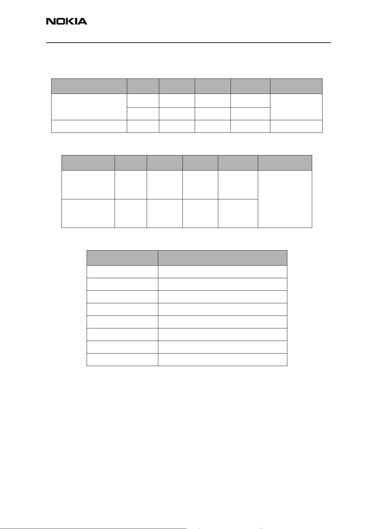
Main technical specifications ......................................................................................9
DC characteristics ..................................................................................................... 9
Internal signals and connections ............................................................................. 12
External signals and connections ............................................................................ 13
Baseband functional description ................................................................................16
Modes of operation.................................................................................................. 16
Battery..................................................................................................................... 17
Charging.................................................................................................................. 19
Supported chargers.................................................................................................. 21
Charger interface protection.................................................................................... 24
Power up and reset .................................................................................................. 24
A/D channels........................................................................................................... 25
Bluetooth................................................................................................................. 26
Keypads................................................................................................................... 27
LCD & keyboard illumination ................................................................................ 27
LCD......................................................................................................................... 29
IR module................................................................................................................ 29
Backup battery......................................................................................................... 29
SIM interface........................................................................................................... 30
System connector .................................................................................................... 31
Internal audio........................................................................................................... 34
Memory block......................................................................................................... 35
RF interface block................................................................................................... 35
Security ......................................................................................................................36
After sales interface ...................................................................................................36
FBUS interface........................................................................................................ 36
MBUS Interface ...................................................................................................... 36
RF................................................................................................................................. 37
Main technical specifications ....................................................................................38
Nominal and maximum ratings............................................................................... 38
RF frequency plan................................................................................................... 38
DC characteristics ................................................................................................... 39
Typical current consumption................................................................................... 40
RF characteristics .......................................................................................................42
Channel numbers and frequencies........................................................................... 42
Main RF characteristics........................................................................................... 42
TX characteristics.................................................................................................... 42
RX characteristics ......................................................................................................43
RF block diagram ......................................................................................................43
Receiver .....................................................................................................................45
Transmitter .................................................................................................................46
Connections ...............................................................................................................46
Issue 1 02/04 ©Nokia Corporation Page 3
Page 4

RH-26
2 - System Module CCS Technical Documentation
Antenna ................................................................................................................... 46
RF-BB interface ...................................................................................................... 47
Page 4 ©Nokia Corporation Issue 1 02/04
Page 5

RH-26
CCS Technical Documentation 2 - System Module
Glossary of Terms
ACI Accessory Control Interface
ADC Analogue-Digital Converter
AEC Acoustic Echo Canceller
AFC Automatic Frequency Control
AGC Automatic Gain Control
AIF Application Interface
ALWE Background noise suppressor
AMS After Market Service
API Application Programming Interface
ARM Processor architecture
ASIC Application Specific Integrated Circuit
BB Baseband
CMT Cellular Mobile Telephone (MCU and DSP)
CPU Central Processing Unit
CTSI Clocking Timing Sleep Interrupt
COG Chip On Glass
CSP Chip Scale Package
CSTN Color Super Twisted Nematic
DAC Digital-Analog Converter
DAI Digital Audio Interface
DB Dual band
DCN Offset Cancellation control signal
DLL Dynamic Link Library
Issue 1 02/04 ©Nokia Corporation Page 5
Page 6

RH-26
2 - System Module CCS Technical Documentation
DRC Dynamic Range Controller
DSP Digital Signal Processor
EGSM Extended – GSM
EFR Enhanced Full Rate
EMC Electromagnetic compatibility
EMI Electromagnetic Interference
ESD Electro Static Discharge
EXT RF External RF
FBUS Asynchronous Full Duplex Serial Bus
GPRS General Packet Radio Service
GSM Global System for Mobile communications
HS Half Rate Speech
HSCSD High Speed Circuit Switched Data
IC Integrated Circuit
IHF Integrated Hands Free
I/O Input/Output
IRDa Infrared Association
LCD Liquid Crystal Display
LDO Low Drop-Out
LNA Low Noise Amplifier
MBUS 1-wire half duplex serial bus
MCU Micro Controller Unit
MDI MCU-DSP Interface
MFI Modulator and Filter Interface
Page 6 ©Nokia Corporation Issue 1 02/04
Page 7

RH-26
CCS Technical Documentation 2 - System Module
PA Transmit Power Amplifier
PC Personal Computer
PCM Pulse Code Modulation
PCM SIO Synchronous serial bus for PCM audio transferring
PIFA Planar Inverted F-antenna
PWB Printed Wiring Board
RF Radio Frequency
SIM Subscriber Identity Module
UEM Universal Energy Management
UI User Interface
UPP Universal Phone Processor
VCXO Voltage Controlled Crystal Oscillator
VCTCXO Voltage Controlled Temperature Compensated Crystal Oscillator.
Issue 1 02/04 ©Nokia Corporation Page 7
Page 8

RH-26
2 - System Module CCS Technical Documentation
System Module
The system module TB6 consists of Radio Frequency (RF) and Baseband (BB) blocks. User
Interface (UI) contains display, keyboard, bluetooth, IR link, HF/HS connector and audio
parts. Part of the keyboard is implemented in a separate flip module, TF6.
The electrical part of the TB6 and half of the qwerty keyboard is located inside the flip
module.
RH-26 includes a Pop-Port™ accessory interface. Both two and three wire type of chargers are supported. BL-5C Li-ion battery with nominal capacity of 850 mAh is used as
main power source.
The baseband blocks provide the MCU, DSP, external memory interface and digital control functions in the UPP ASIC. Power supply circuitry, charging, audio processing and RF
control hardware are located in the UEM ASIC.
The purpose of the RF block is to receive and demodulate the radio frequency signal from
the base station and to transmit a modulated RF signal to the base station.
Page 8 ©Nokia Corporation Issue 1 02/04
Page 9
RH-26
y
j
µ
CCS Technical Documentation 2 - System Module
Baseband
Technical summary
The main functionality of the baseband is implemented into two ASICs:
- UPP (Universal Phone Processor) and
- UEMK Edge (Universal Energy Management)
Figure 1: Baseband block description
UPP8Mv3
Combo
Memor
FLASH 128Mbit
& utRAM 16MBit
Keyboards
Engine QWERTY
Engine control
Flip T9
C
Flip QW ERTY
LCD
Passive colour STN
Led driver
Keyboard &
display
illumination
SIM
DEMI
RF-BB Interface
UEMK
Edge
1.8 V
Battery
BL-5C
BU
IR
Bluetooth
Vibra
Accessory
Regulator
System connector
DC
ack
IHF
IHF Amp
LM4890
HWA
Baseband is running from power rails 2.8V analog voltage and 1.8V I/O voltage. UPP core
voltages can be programmed to 1.053V, 1.35V, 1.57V (default) and 1.8V. UEMK includes
a 6-linear LDO (low drop-out) regulator for baseband and 7 regulators for RF. It also
includes 4 current sources for biasing purposes and internal usage. UEMK also includes
SIM interface, which supports both 1.8V and 3V SIM cards.
The baseband architecture supports a power saving function called ”sleep mode”. This
sleep mode shuts off the VCTCXO, which is used as system clock source for both RF and
baseband. During the sleep mode, the system runs from a 32 kHz crystal. The phone is
waken up by a timer running from this 32 kHz clock supply or from external interrupt.
The sleeping time is determined by network parameters. The sleep mode is entered when
both the MCU and the DSP are in standby mode and the normal VCTCXO clock has been
switched off. Bluetooth has its own sleep period that is not aligned with phone sleep.
CSR BC02
Camera
CIF
Issue 1 02/04 ©Nokia Corporation Page 9
Page 10
RH-26
2 - System Module CCS Technical Documentation
A real time clock function is integrated into the UEMK, which utilises the same 32kHz
clock supply as the sleep clock. A backup power supply is provided for the RTC-battery,
which keeps the real time clock running when the main battery is removed. The backup
power supply is a rechargeable surface mounted cell capacitor. The backup time with the
cell capacitor is 15 minutes minimum.
The interface between the baseband and the RF section is mainly handled by a UEMK
ASIC. UEMK provides A/D and D/A conversion of the in-phase and quadrature receive and
transmit signal paths and also A/D and D/A conversions of received and transmitted
audio signals to and from the user interface. The UEMK supplies the analog TXC and AFC
signals to the RF section according to the UPP DSP digital control. Data transmission
between the UEMK and the UPP is implemented using two serial busses, DBUS for DSP
and CBUS for MCU. There are also separate signals for PDM coded audio. Digital speech
processing is handled by the DSP inside UPP ASIC. UEMK is a dual voltage circuit, the
digital parts are running from the baseband supply 1.8V and the analogue parts are running from the analogue supply 2.78V also VBAT is directly used by some specific blocks.
The baseband supports both internal and external microphone inputs and speaker outputs. Input and output signal source selection and gain control is done by the UEMK
according to control messages from the UPP. Keypad tones, DTMF, and other audio tones
are generated and encoded by the UPP and transmitted to the UEMK for decoding. An
external vibra alert control signal is generated by the UEMK with separate PWM output.
RH-26 has two external serial control interfaces: FBUS and MBUS. FBUS can be accessed
through service test pattern and Pop-PortTM System Connector. FBUS interface and
MBUS can be accessed through the service test pattern.
EMC shielding is implemented using soldered metal cans. Heat generated by the circuitry
is conducted out via ground planes located in the PWB.
The RH-26 PWB is implemented into an 8-layer selective OSP coated PWB using buried
via technology.
Main technical specifications
DC characteristics
Regulators and supply voltage ranges
Table 1: Baseband regulators
Signal Min Nom Max Note
VANA 2.70V 2.78V 2.86V I
VFLASH1 2.70V 2.78V 2.86V I
VFLASH2 2.70V 2.78V 2.86V I
max
max
I
sleep
max
= 80mA
= 70mA
= 1.5mA
= 40mA
Page 10 ©Nokia Corporation Issue 1 02/04
Page 11
RH-26
CCS Technical Documentation 2 - System Module
VSIM 1.745V
2.91V
VIO 1.72V 1.8V 1.88V I
VCORE 1.0V
1.283V
1.492V
1.710V
1.8V
3.0V
1.053V
1.35V
1.57V
1.8V
1.855V
3.09V
1.106V
1.418V
1.649V
1.890V
I
= 25mA
max
I
= 0.5mA
sleep
= 150mA
max
= 0.5mA
I
sleep
I
= 200mA
max
I
= 0.2mA
sleep
Default value 1.57V
Table 2: Accessory regulator
Signal Min Nom Max Note
Vout 2.70V 2.78 2.86V I
= 150mA
max
I
quiescent
< 1.5µA
Enable controlled
through GenIO(0)
Table 3: RF regulators
Signal Min Nom Max Note
VR1A / VR1B 4.6V 4.75V 4.9V I
VR2 2.70V
3.20V
2.78V
3.3V
2.86V
3.40V
VR3 2.70V 2.78V 2.86V I
VR4 2.70V 2.78V 2.86V I
VR5 2.70V 2.78V 2.86V I
VR6 2.70V 2.78V 2.86V I
VR7 2.70V 2.78V 2.86V I
max
I
max
max
max
I
sleep
max
I
sleep
max
I
sleep
max
= 10mA
= 100mA
= 20mA
= 50mA
= 50mA
= 50mA
= 45mA
Table 4: Current sources
Signal Min Nom Max Note
IPA1 and IPA2 0mA – 5mA Programmable, +/-6%
V
= 0V - 2.7V
IPA1,2
= 0.1mA
= 0.1mA
= 0.1mA
IPA3 and IPA4 95µA 100µA 105µA V
IPA3,4
= 0V - 2.7V
(used internally in the UEMK)
Issue 1 02/04 ©Nokia Corporation Page 11
Page 12
RH-26
y
2 - System Module CCS Technical Documentation
Table 5: External BT regulator characteristics
Power source Voltage (V)
Max. load
(mA)
Function
Min Typ Max
VBth 2.72 2.80 2.86 70mA From external 2.8V reg-
ulator
VIO 1.72 1.80 1.88 10 mA I/O-voltage to ensure
compatible IO levels.
Table 6: External camera regulator characteristics
Power source Voltage (V)
Max. load
(mA)
Function
Min Typ Max
VCAMDIG 1.72 1.80 1.88 150 mA I/O-voltage to ensure com-
patible IO levels.
Figure 2: Power distribution diagram
Baseband
BT
Camera
VLED+
White LED
Driver
Battery
Reg.
2.8V
Reg.
1.8V
VBAT
VBAT
Audio
Amplifier
PA Supply
UEM
RTC
RF Regulators
VFLASH2
Baseband
Regulators
CHACON
Accessory
Regulator
Vout
System Connector
VR1A
VR1B
VR2-7
VSIM
VCORE
VANA
VIO
VFLASH1
6
SIM
UPP
Combo
Memor
LCD
Backup
battery
IRDA
VBAT
Page 12 ©Nokia Corporation Issue 1 02/04
Page 13
RH-26
CCS Technical Documentation 2 - System Module
Internal signals and connections
Table 7: Internal microphone
Signal Min Nom Max Condition Note
MICP 200mV
2.0 V 2.1 V 2.25 V DC
MICN 2.0V 2.1V 2.25V DC
Table 8: Internal speaker
Signal Min Nom Max Condition Note
EARP
0.75V 0.8V
EARN
0.75V 0.8V
Table 9: Bluetooth clock specifications
Bluetooth clock Specification
BTClk Single ended input
2.0 V
0.85V
2.0 V
0.85V
pp
pp
AC 2.2kΩ to MIC1B
pp
AC
DC
AC
DC
Differential output
(V
= 4.0 Vpp)
diff
Frequency 26MHz (VCTCXO)
Min. level 200 mVpp
Max. level 1.8 Vpp (VIO)
Input impedance Input impedance < 4 pF and >10kohm
Phase noise Max. –129 dBc/Hz @ 1 kHz at 26 MHz
Phase Jitter 15ps rms
Settling time Max. 5ms (BTHostWakeUp -> BTClk stabile)
Issue 1 02/04 ©Nokia Corporation Page 13
Page 14
RH-26
2 - System Module CCS Technical Documentation
External signals and connections
Table 10: UI connector
Pin Signal Min Nom Max Condition Note
16 VDDI 1.72V 1.8V 1.88V Logic voltage supply
Connected to VIO
15 XRES 0.7*VDDI
0
1us t
14 SDA 0.7*VDDI
0
100ns t
100ns t
13 SCLK 0.7*VDDI
0
250ns t
100ns t
100ns t
12 CXS 0.7*VDDI
0
60ns t
VDDI
0.3*VDDI
VDDI
0.3*VDDI
VDDI
0.3*VDDI
6.5MHz
VDDI
0.3*VDDI
Logic ’1’
Logic ’0’
rw
Logic ’1’
Logic ’0’
sds
sdh
Logic ’1’
Logic ’0’
Max frequency
scyc
shw
slw
Logic ’1’
Logic ’0’
css
Reset
Active low
Reset active
Serial data
Data setup time
Data hold time
Serial clock input
Clock cycle
Clock high
Clock low
Chip select
Active low
CXS low before SCLK rising
edge
100ns t
csh
CXS low after SCLK rising edge
11 GND 0V
10 GND 0V
9 GND 0V
8 GND 0V
7 GND 0V
6 GND 0V
5 VDD VDD 2.70V 2.78V 2.86V Supply Voltage.
Connected to VFLASH1
4 GND 0V
3 GND 0V
2 VLED- 0V
0.5V
LED off
LED on
Feedback Voltage to LED Driver
Page 14 ©Nokia Corporation Issue 1 02/04
Page 15
RH-26
CCS Technical Documentation 2 - System Module
1 VLED+ 0V
9V
LED off
LED on
Supply Voltage for LEDs
Table 11: FLIP connector
Pin Signal Min Nom Max Condition Note
1 FLIPCLK 0.7*VIO
0
VIO
0.3*VIO
Logic ’1’
Logic ’0’
Bus clock for flip
module
2 VBAT 3.7V 4.2V Supply for flip µC
3 FLIPDATA 0.7*VIO
0
VIO
0.3*VIO
Logic ’1’
Logic ’0’
I/O data for flip
module
Table 12: DC connector
Pin Signal Min Nom Max Condition Note
1 VCHAR 11 . 1V
7.0 V
RMS
8.4 V
peak
RMS
16.9 V
7.9 V
1.0 A
9.2 V
850 mA
peak
RMS
peak
RMS
Standard
charger
Fast charger
Charger positive
input
2 CHGND 0 Charger ground
Table 13: Pop-Port
TM
system connector
Pin Signal Description Spectral Range U/I levels Impedance Notes
1 CHARGE V Charge DC 0-9 V / 0.85 A
2 GND Charge GND 0.85 A 100 mΩ (PWB + conn.)
3 ACI ACI 1 kbit/s Dig 0 / 2.78V 47 Ω Insertion & removal
detection
4 VOUT DC out DC 2.78V / 70mA 100 mΩ (PWB + conn.) 200mW
5 NC DC in DC 4.375-5.25V
6 FBUS RX FBUS 115k FBus 0 / 2.78V 33 Ω
7 FBUS TX FBUS 115k FBus 0 / 2.78V 33 Ω
8 GND Data GND
9 XMIC N Audio in 300 - 8k 1Vpp & 2.78V DC
10 XMIC P Audio in 300 - 8k 1Vpp & 2.78V DC
11 HSEAR N Audio out 20 - 20k 1Vpp 10 Ω
12 HSEAR P Audio out 20 - 20k 1Vpp 10 Ω
13 NC Not Connected
Issue 1 02/04 ©Nokia Corporation Page 15
Page 16

RH-26
2 - System Module CCS Technical Documentation
14 NC Not Connected
Table 14: SIM connector
Pin Name Parameter Min Typ Max Unit Notes
1 VSIM 1.8V SIM Card 1.62 1.8 1.98 V Supply voltage
3V SIM Card 2.7 3.0 3.3 V
2 SIMRST 1.8V SIM Card 0.8xVSIM
0
3V SIM Card 0.8xVSIM
0
3 SIMCLK Frequency 3.25 MHz SIM clock
Trise/Tfall 50 ns
1.8V Voh
1.8V Vol
3V Voh
3V Vol
4 DATA 1.8V Voh
1.8V Vol
3V Voh
3V Vol
1.8V Vih
1.8V Vil
3V Vil
3V Vil
0.7xVSIM
0
0.7xVSIM
0
0.7xVSIM
0
0.7xVSIM
0
0.7xVSIM
-0.3
0.7xVSIM
-0.3
VSIM
0.2xVSIM
VSIM
0.2xVSIM
VSIM
0.2xVSIM
VSIM
0.2xVSIM
VSIM
0.3
VSIM
0.4
VSIM +0.3
0.2xVSIM
VSIM +0.3
0.2xVSIM
V SIM reset (output)
V
V
V
V SIM data (output)
V
V SIM data (input)
Trise/Tfall max 1us
5 NC Not connected
6 GND GND 0 0 V Ground
Page 16 ©Nokia Corporation Issue 1 02/04
Page 17

RH-26
CCS Technical Documentation 2 - System Module
Baseband functional description
Modes of operation
RH-26 baseband engine has six different functional modes:
• No supply
• Back-up
•Acting Dead
•Active
• Sleep
• Charging
No supply
In NO_SUPPLY mode, the phone has no supply voltage. This mode is a result of disconnection of the main and backup batteries or low battery voltage level in both of the batteries.
Phone is exiting from NO_SUPPLY mode when sufficient battery voltage level is detected.
Battery voltage can rise either by connecting a new battery with VBAT > V
connecting charger and charging the battery above V
Back-up
In BACK_UP mode, the backup battery has sufficient charge but the main battery can be
disconnected or empty (VBAT < V
VRTC regulator is disabled in BACK_UP mode. VRTC output is supplied without regulation
from backup battery (VBACK). All the other regulators are disabled in BACK_UP mode.
Acting dead
If the phone is off when the charger is connected, the phone is powered on but enters a
state called ”Acting Dead”. To the user, the phone acts as if it was switched off. A battery
charging alert is given and/or a battery charging indication on the display is shown to
acknowledge the user that the battery is being charged.
and VBACK > VBU
MSTR
MSTR+
COFF
or by
MSTR+
.
).
Active
In the ACTIVE mode, the phone is operates normally, scanning for channels, listening to a
base station, transmitting and processing information. There are several sub-states in the
active mode depending on if the phone is in burst reception, burst transmission, if DSP is
working, etc.
In the Active mode, the RF regulators are controlled by SW, which writes the desired settings into UEMK’s registers: VR1A can be enabled or disabled. VR2 can be enabled or dis-
Issue 1 02/04 ©Nokia Corporation Page 17
Page 18

RH-26
2 - System Module CCS Technical Documentation
abled and its output voltage can be programmed to be 2.78V or 3.3V. VR4 -VR7 can be
enabled, disabled, or forced into low quiescent current mode. VR3 is always enabled in
the Active mode.
Sleep mode
SLEEP mode is entered when both MCU and DSP are in stand–by mode. Sleep is controlled by both processors. When SLEEPX low signal is detected, UEMK enters the SLEEP
mode. VCORE, VIO and VFLASH1 regulators are put into low quiescent current mode. All
the RF regulators are disabled in SLEEP. When SLEEPX=1 is detected, UEMK enters the
ACTIVE mode, which activates all functions.
The sleep mode is exited either by the expiration of a sleep clock counter in the UEMK or
by some external interrupt, generated by a charger connection, key press, headset connection, etc.
In the sleep mode, VCTCXO is shut down and a 32 kHz sleep clock oscillator is used as a
reference clock for the baseband.
Charging
Battery
Charging can be performed in any operating mode. The battery type/size is indicated by a
resistor inside the battery pack. The resistor value corresponds to a specific battery
capacity. This capacity value is related to the battery technology as different capacity
values are achieved by using different battery technology.
The battery voltage, temperature, size and current are measured by the UEMK controlled
by the charging software running in the UPP.
The charging control circuitry inside the UEMK controls the charging current delivered
from the charger to the battery. The battery voltage rise is limited by turning the UEMK
switch off when the battery voltage reaches 4.2 V. Charging current is monitored by
measuring the voltage drop across a 220 mΩ resistor.
850 mAh Li-ion battery pack BL-5C is used in RH-26.
Table 15: BL-5C characteristics
Description Value
Nominal discharge cut-off voltage 3.1V
Nominal battery voltage 3.7V
Nominal charging voltage 4.2V
Maximum charger output current 850 mA
Minimum charger output current 200 mA
Discharge Temperature -20 °C… +70 °C
Page 18 ©Nokia Corporation Issue 1 02/04
Page 19

RH-26
CCS Technical Documentation 2 - System Module
Charging Temperature -30 °C… +60 °C
Table 16: Pin numbering of battery pack
Signal name Pin number Function
VBAT 1 Positive battery terminal
BSI 2 Battery capacity measurement (fixed resistor inside the battery pack)
GND 3 Negative/common battery terminal
Figure 3: BL-5C battery pack contacts
3(GND)
1 (+)2(BSI)
The BSI fixed resistor value indicates type and default capacity of a battery. NTC-resistor
measures the battery temperature.
Temperature and capacity information is needed for the charge control. BSI is connected
to a pin in the battery connector. BTEMP is connected to NTC resistor. NTC is located on
the engine PWB. Phone has 100 kΩ pull-up resistors for these lines so that they can be
read by A/D inputs in the phone.
Table 17: BSI resistor values
Parameter Min Typ Max
Battery size indicator resistor
BSI
6.7 6.8 6.9 kΩ Test mode resistor value
3.2 3.3 3.4 kΩ Local mode resistor value
75 kΩ Battery size indicator (BL-5C)
Uni
t
Notes
Tolerance ±1%
Table 18: BTEMP NTC resistor properties
Parameter Min Typ Max
NTC resistor BTEMP 47 kΩ Battery temperature indicator (NTC
4050 K Beta value (B).
Uni
Notes
t
pulldown) ±5% @ 25°C
Tolerance ±3%, +25°C / +85°C
Issue 1 02/04 ©Nokia Corporation Page 19
Page 20

RH-26
2 - System Module CCS Technical Documentation
Figure 4: Interconnection diagram
Charging
Supported chargers are ACP-7, ACP-8, ACP-9, ACP-12, LCH-8, LCH-9 and LCH-12.
Charging is controlled by the UEMK ASIC. External components are needed for current
sensing, EMC, reverse polarity and transient protection of the input to the baseband
module. The charger is connected to the system connector interface. The RH-26 baseband is designed to support DCT3 chargers. Both 2- and 3-wire type chargers are supported.
The operation of the charging circuit has been specified in such a way as to limit the
power dissipation across the charge switch and to ensure safe operation in all modes.
VBATT
GND
BSI
Li-Ion
Overcharge /
Overdischarge
protection
Page 20 ©Nokia Corporation Issue 1 02/04
Page 21

RH-26
CCS Technical Documentation 2 - System Module
Figure 5: UEMK charging circuitry
Charger detection
When connected, a charger creates voltage on VCHAR input of the UEMK. When VCHAR
input voltage level is detected to have risen above VCH
threshold by CHACON, the
DET+
charging process starts. VCHARDET signal is generated to indicate the presence of the
charger. The charger identification is controlled by EM SW.
The charger recognition is initiated when the EM SW receives a ”charger connected”
interrupt. The algorithm consists of the following three steps:
1 Check that the charger output (voltage and current) is within safety limits.
Issue 1 02/04 ©Nokia Corporation Page 21
Page 22

RH-26
2 - System Module CCS Technical Documentation
2 Identify the charger as a two-wire or three-wire charger.
3 Check that the charger is within the charger window.
If the charger is accepted and identified, the appropriate charging algorithm is initiated.
Charge control
In the active mode, charging is controlled by UEMK’s digital part. Charging voltage and
current monitoring is used to limit charge into safe area. For that reason, UEMK has programmable charging cut–off limits VBATLim
(3.6V / 5.0V /5.25V). Maximum
1,2L,2H
charging current is limited to 1.2 A. Default for VBATLim is 3.6V.
VBATLim
+ charging is stopped by turning charging switch OFF. There is no change in oper-
1,2L,2H
are designed with hysteresis. When the voltage rises above VBATLim
1,2L,2H
ational mode. After voltage has decreased below VBAT-Lim–, charging re–starts.
If VBAT is detected to have risen above the programmed limit, the output signal OVV is
set to ‘1’ by CHACON. If charging current limit is reached, OVC output is set to ‘1’ by
CHACON (disabled by EM SW).
Pulse–width–Modulated (PWM) control signals PWM1 and PWM32 are generated by
UEMK’s digital part to CHACON block. There are two PWM frequencies in use depending
on the type of the charger: standard charger 1Hz, fast charger 32Hz. Duty cycle range is
from 0% to 100%.
Supported chargers
Transformer type chargers
The standard charger (ACP-7) has a mains transformer with a typical output impedance
of 11.1 Ω. It has a full-wave rectified output with no smoothing capacitor on the output.
As charging circuitry gets its supply from the charger, voltage UEMK must be able to
generate supply voltage for needed control from full wave rectified charger input.
Table 19: ACP-7 characteristics
Description Min. Typ. Max. Unit
Output impedance (at +23*C) 10.1 11 . 1 12.1 W
Output voltage (average) with 5 kΩ load 7.25 7.6 7.95 V
Output voltage (peak) with 5 kΩ load and with max. (Nominal
+20%) mains voltage.
16.9 V
Page 22 ©Nokia Corporation Issue 1 02/04
Page 23

RH-26
CCS Technical Documentation 2 - System Module
Figure 6: Transformed type charger window (U/I curve)
Figure 7: Full-wave rectified output of standard charger
Current limited constant voltage chargers
2- and 3-wire current limited constant voltage chargers are supported.
3-wire chargers:
•ACP-9
•LCH-9
2-wire chargers:
Issue 1 02/04 ©Nokia Corporation Page 23
Page 24

RH-26
2 - System Module CCS Technical Documentation
•ACP-8
•ACP-12
•LCH-8
•LCH-12
The 3-wire chargers have a 3-wire interface to the phone, 2 power and 1 control. To control the charger output voltage, the wire carries a 32Hz digital pulse width modulated
signal generated by the phone. In RH-26, 32 Hz PWM for the charger is connected to
GND inside the bottom connector. This sets full charger output voltage and equals to 0%
PWM from the charger point of view.
The output capacity of a fast charger is typically 1000uF. The cable impedance (from output capacitor to the phone) is typically 0.5 Ω.
Figure 8: U/I specification at control input 0% or without control
Page 24 ©Nokia Corporation Issue 1 02/04
Page 25

RH-26
CCS Technical Documentation 2 - System Module
Charger interface protection
In order to ensure safe operation with all chargers and in misuse/fail situations, the
charger interface is protected by using a transient voltage suppressor (TVS) and 1.5A
fuse. TVS used in RH-26 is a 16V@175W device.
Table 20: TVS characteristics
Parameter Value
Breakdown voltage (VBR) 17.8 Vmin (at IT 1.0mA)
Reverse standoff voltage (VR) 16V
Max reverse leakage current at VR (IR) 5uA
Max peak impulse current (Ipp)
(at Ta=25*C and peak impulse current waveform:
10/1000us)
Max clamping voltage at Ipp (Vc) 26V
Power up and reset
Power up and reset is controlled by the UEMK ASIC. RH-26 baseband can be powered up
in the following ways:
• Press power button, meaning grounding the PWRONX pin on UEMK.
• Connect the charger to the charger input.
• Supply battery voltage to the battery pin.
• RTC Alarm, the RTC has been programmed to give an alarm.
After receiving one of the above signals, the UEMK counts a 20ms delay and then enters
its reset mode. The watchdog starts up, and if the battery voltage is greater than Vcoff+,
a 200ms delay is started to allow references to settle. After this delay elapses, the
VFLASH1 regulator is enabled. 500us later VR3, VANA, VIO and VCORE are enabled.
Finally, the PURX line is held low for 20 ms. This reset, PURX, is fed to the baseband ASIC
UPP. Resets are generated for the DSP and the MCU. During this reset phase the UEMK
forces the VCXO regulator on, regardless of the status of the sleep control input signal to
the UEMK. The sleep signal from the ASIC is used to reset the flash during the power up
mode and to put the flash in the power down mode during sleep. All baseband regulators
are switched on at the UEMK power on, except the SIM regulator that is controlled by
the MCU. The UEMK internal watchdog is running during the UEMK reset state, with the
longest watchdog time selected. If the watchdog expires, the UEMK returns to power off
state. The UEMK watchdog is internally acknowledged at the rising edge of the PURX signal in order to always give the same watchdog response time to the MCU.
7A
Power up with PWR key
When the power on key is pressed, the UEMK enters the power up sequence as described
in the previous paragraph. Pressing the power key causes the PWRONX pin on the UEMK
Issue 1 02/04 ©Nokia Corporation Page 25
Page 26

RH-26
2 - System Module CCS Technical Documentation
to be grounded. The UEMK PWRONX signal is not part of the keypad matrix. The power
key is only connected to the UEMK. This means that when pressing the power key, an
interrupt is generated to the UPP that starts the MCU. The MCU then reads the UEMK
interrupt register and notices that it is a PWRONX interrupt. The MCU now reads the status of the PWRONX signal using the UEMK control bus, CBUS. If the PWRONX signal
stays low for a certain time, the MCU accepts this as a valid power on state and continues with the SW initialization of the baseband. If the power on key does not indicate a
valid power on situation, the MCU powers off the baseband.
Power up when charger is connected
In order to be able to detect and start charging in a case where the main battery is fully
discharged (empty), and hence UEMK has no supply (NO_SUPPLY or BACKUP mode of
UEMK), charging is controlled by the START-UP CHARGING circuitry.
Whenever VBAT level is detected to be below master reset threshold (VMSTR-), charging
is controlled by START_UP charge circuitry. Connecting a charger forces VCHAR input to
rise above charger detection threshold, VCHDET+. Upon detection, start-up charging is
started. UEMK generates 100mA constant output current from the connected charger’s
output voltage. As battery charges, its voltage rises, and when VBAT voltage level is
higher than master reset threshold limit (VMSTR+), charge is terminated.
Charge control block (CHACON) monitors the VBAT voltage level. MSTRX=‘1’ output reset
signal (internal to UEMK) is given to UEMK’s RESET block when VBAT>VMSTR+. UEMK
enters the reset sequence.
If VBAT is detected to fall below VMSTR- during start-up charging, charging is cancelled.
Charging will restart, if new rising edge on VCHAR input is detected (VCHAR rising above
VCHDET+).
Power up when battery is connected
Baseband can be powered up by connecting battery with sufficient voltage. Battery voltage has to be over UEMK internal comparator threshold level, Vcoff+. When battery voltage is detected, UEMK enters the reset sequence.
Phone can be powered up to LOCAL mode by setting BSI resistor to 3.3kΩ. This causes
MCU to wake up directly when battery voltage is supplied.
RTC alarm power up
If phone is in power off mode when an RTC alarm occurs, the wake up follows the procedure described in section Power up and reset. After baseband is powered on, an interrupt
is given to MCU. When RTC alarm occurs during power on state, the interrupt for MCU is
generated.
A/D channels
The UEMK contains following A/D converter channels that are used for several measurement purposes. The general slow A/D converter is a 10-bit converter using the UEMK
interface clock for the conversion. An interrupt is given at the end of the measurement.
Page 26 ©Nokia Corporation Issue 1 02/04
Page 27

RH-26
CCS Technical Documentation 2 - System Module
The UEMK’s 11-channel analogue to digital converter is used to monitor charging functions, battery functions, user interface and RF functions.
Bluetooth
A single chip bluetooth BC02-ROM is used in RH-26.
Figure 9: Baseband-BT connections
Vbat
CBUSClk
HELGO
UPP8Mv3
VR3
PURX
VIO
2.8V
LDO
BC02-ROM
Vreg_in
VDD_VIO
GenIO 14 (PCMClk)
GenIO 16 (PCMRx)
GenIO 15 (PCMTx)
GenIO 17 (PCMSync)
GenIO 8 (BTRstX)
GenIO 19 (BTUARTRx)
GenIO 20 (BTUARTTx)
GenIO 11 (UPP_BT_CTS)
GenIO 12 (BTHostWakeup)
GenIO 21 (UPP_BT_RTS)
GenIO 10(BTWakeup)
Xtal_in
PCM_clk
PCM_out
PC_Min
PCM_sync
ResetB VDD_radio
UART_tx VDD_vco
UART_rx VDD_core
UART_rts_p[PIO2]
Host_wakeup [PIO6]
UART_cts_P [PIO3]
UART_cts PIO[0-11]
BT_Wakeup [PIO4]
1.8V
VDD_ANA
The BB and BC02 interface can be logically divided into audio, user data and control
interfaces.
User and control data is transferred through the UART interface. Audio is using a PCM
interface of the UPP.
A BC02 internal voltage regulator provides 1.8V supply for the analogue and digital sections of BC02. An external 2.8V regulator is used to ensure that the input voltage to the
BC02 internal regulator is within the recommended operating range. VIO is directly used
as a supply for IO interface.
Camera
The camera supports a video preview mode with integrated color processing, and high
Issue 1 02/04 ©Nokia Corporation Page 27
Page 28
RH-26
2 - System Module CCS Technical Documentation
quality still image mode. The camera module supports the CCP/CCI interface.
The camera module supports a sleep and shutdown functions in order to minimize the
current consumption when not used.
In viewfinder mode the device outputs RGB 4:4:4 pixel data for the color LCD display.
Keypads
RH-26 consists of a separate flip board, TF6, which includes contacts for the qwerty and
T9 keypad domes, MCU, led driver and LEDs for keypad lighting. The flip board is connected to the main PWB through a 3-pin flip connector interface with coaxial cables.
Signals of the connector are described in section: External signals and connections.
The keyboard of RH-26 consists of qwerty keypads located on the top side of the engine
PWB and the FLIP module.
Keypad signals of the engine qwerty keypad are connected to the UPP keyboard interface. The flip keypad is connected to the MCU located in the flip PWB. Key presses are
sent to engine through a 2-wire serial interface. The implementation of the engine and
flip keypad is similar.
LCD & keyboard illumination
In RH-26, white LEDs are used for LCD and keypad lighting. Three LEDs are used for LCD
lighting and on the engine side eight LEDs for qwerty keypad and soft key lighting. A
step-up DC-DC converter (LM3500) is used as a LED driver. On the flip module, four LEDs
are used for T9 and four LEDs for the qwerty keypad lighting.
LCD LEDs are driven in a serial mode to achieve stable backlight quality. This means constant current flow through LCD LEDs. Serial resistance Rlcd is used to define the proper
current. The feedback signal, FB, is used to control the current. Driver increases or
decreases the output voltage for LEDs in order to keep the current stable.
Page 28 ©Nokia Corporation Issue 1 02/04
Page 29

RH-26
CCS Technical Documentation 2 - System Module
Engine qwerty keypad LEDs are driven in 2 serial mode with each branch having its own
current limiting resistor. Serial resistance R is used to limit the current through the LEDs.
The feedback signal, FB, from LCD LEDs controls also the current of keypad LEDs. Qwerty
LEDs are controlled through UEMK CALLED1 pin.
Driver is controlled by the UEMK via DLight output. This signal is connected to driver ENpin (on/off).
Figure 10: Engine board LCD and keyboard LED connections
On the flip module, there is a transistor based “constant current” circuitry for LED driving. A diode is used to set the reference voltage, and resistors, Rs, are used to set the current through transistor and LEDs.
LED drivers are controlled by the MCU I/O-pins. By setting either (qwerty & T9) of the
control signals “high”, the driver is enabled for the selected keypad.
Figure 11: Flip LED driver circuitry
Issue 1 02/04 ©Nokia Corporation Page 29
Page 30

RH-26
2 - System Module CCS Technical Documentation
LCD
A passive matrix colour STN display having 128 x 128 8 bpp (bits per pixel) is used in RH-
26. The LCD display is connected to the transceiver PWB by a board-to-board connector.
Table 21: LCD characteristics
Technology CSTN
Display format 128 columns x 128 rows
Weight estimation 7 g
Illumination Mode
RAM bit data
Numbers of colours 256 (8 bits per pixel, 3 x Red, 3 x Green & 2 x Blue)
Colour filter arrangement Stripe (RGB)
Pixel height to width ratio 1:1
Main viewing direction 6 o’clock
IR module
The IR interface is designed into the UPP. The IR link supports speeds from 9600 bit/s to
1.152 MBit/s up to distance of 100 cm (75 cm with 1.152Mbit/s). Transmission over the
IR if half-duplex.
The length of the transmitted IR pulse depends on the speed of the transmission. When
230.4 kbit/s or less is used as a transmission speed, pulse width is maximum1.63µs. If
transmission speed is set to 1.152Mbit/s, the nominal pulse width is 154ns.
Backup battery
A backup battery is used when the main battery is either removed or discharged. The
backup battery is used for keeping real-time clock running for a minimum of 10 minutes.
Transreflective
"0000"…OFF (minimum voltages) Black
The rechargeable backup battery is connected between UEMK VBACK and GND. In UEMK,
the backup battery charging high limit is set to 3.2V. The cut–off limit voltage (V
BUCoff– ) for the backup battery is 2.0V. Charging is controlled by the MCU by writing
into UEMK register.
Cell capacitor SMD “battery” type is used. The nominal capacity of the battery is 0.01
mAh.
Table 22: Backup battery circuitry
Parameter
Test conditions
Back-up battery voltage VBACK 2.43 3.3 V
Symbol Min Typ Max Unit
Page 30 ©Nokia Corporation Issue 1 02/04
Page 31

RH-26
CCS Technical Documentation 2 - System Module
Back-up battery cut-off
limit
Charging voltage (VBAT ?
3.4V)
Charging current I
SIM interface
The UEMK contains the SIM interface logic level shifting. The SIM interface can be programmed to support 3V and 1.8V SIMs. SIM supply voltage is selected by a register in the
UEMK. It is only allowed to change the SIM supply voltage when the SIM IF is powered
down.
The SIM comparator offset is such that the comparator outputs do not alter state as long
as the battery is connected. The threshold voltage is calculated from the battery size
specifications.
The whole SIM interface is located in two chips, namely UPP and UEMK.
The SIM interface in the UEMK contains power up/down, port gating, card detect, data
receiving, ATR-counter, registers and level shifting buffers logic. The SIM interface is the
electrical interface between the Subscriber Identity Module Card (SIM Card) and mobile
phone (via UEMK device).
V_BU
COFF+
V_BU
COFF-
VBU 3.1 3.2 3.3 V
LIMVBU
2.04
1.94
150 500 µA
2.10
2.0
2.16
2.06
V
V
The data communication between the card and the phone is asynchronous half duplex.
The clock supplied to the card is in GSM system 3.25 MHz. The data baudrate is SIM card
clock frequency divided by 372 (by default), 64, 32 or 16. The supported protocol type,
that is T=0 (asynchronous half-duplex character transmission as defined in ISO 7816-3).
Issue 1 02/04 ©Nokia Corporation Page 31
Page 32

RH-26
2 - System Module CCS Technical Documentation
Figure 12: UPP/UEMK SIM interface connections
GND
UPP
SIM
C5 C6 C7
C1C2C3
From Battery Type contact
C8
C4
BSI
SIMDATA
SIMCLK
SIMRST
VSIM
GND
UEM
SIMIF
register
SIMIO
SIMClk
Data
UEM
digital
logic
SIMIO
SIMClk
Data
UIF Block
UEMInt
CBusDa
CBusEnX
CBusClk
The internal clock frequency from CTSI block is 13 MHz in GSM. To achieve the minimum
starting SIMCardClk rate of 3.25 MHz and the duty cycle requirement between 40% and
60%, the slowest possible clock supplied to the SIM has to be in the GSM system clock
rate of 13/4 MHz.
System connector
The system connector in RH-26 is called Pop-PortTM System Connector. It consists of
charging plug socket and system connector. In RH-26, the system connector includes:
Function Note
Charging Pads for 2 -wire charging in cradles
Audio - 2 -wire fully differential mono audio output
Power Supply for Accessories 2.78V 70 mA output to accessories (DCT4)
ACI (Accessory Control Interface) Accessory detection/removal & controlling
FBUS Standard FBUS
- 2-wire differential microphone input
Page 32 ©Nokia Corporation Issue 1 02/04
Page 33

RH-26
y
CCS Technical Documentation 2 - System Module
Figure 13: Pop-PortTM system connector (charger plug socket & system connector)
ACI
ACI (Accessory Control Interface) is a point-to-point, bi-directional serial bus. ACI has
two main features: 1) The insertion and removal detection of an accessory device 2) acting as a data bus, intended mainly for control purposes. A third function provided by ACI
is to identify and authenticate the specific accessory which is connected to the system
connector interface.
External accessory regulator
An external LDO Regulator is needed for accessory power supply purposes. All ACI-accessories require this power supply. Regulator input is connected to battery voltage VBAT
and output is connected to Vout pin in system connector. Regulator is controlled via UPP
(On/Off-function).
Figure 14: Accessory power supply diagram
System Connector
VBAT
UPP
Genio(0)
Signal Min Nom Max Note
Vout 2.70V 2.78 2.86V I
GenIO(0) 1.4 1.8 1.88
Accessor
Regulator
Table 23: Accessory regulator signals
0.6
Vout
= 150mA
max
High (ON)
Low (OFF)
External audio
RH-26 is designed to support fully differential external audio accessory connection. A
headset can be directly connected to the system connector. Only mono audio is supported. With RH-26, two different kinds of headsets can be used: stereo or mono headset.
Headset implementation uses separate microphone and earpiece signals. The accessory is
detected by the HeadInt signal when the plug is inserted. Normally when no plug is
present, the internal pull-down on the HF pin pulls down the HeadInt signal. Because of
Issue 1 02/04 ©Nokia Corporation Page 33
Page 34

RH-26
2 - System Module CCS Technical Documentation
that the comparator level is 1.9V. The HeadInt signal does not change the state, even if
the HF output is biased to 0.8V. When the plug is inserted, the switch is opened and the
HeadInt signal is pulled up by the internal pull-up. The 1.9V threshold level is reached
and the comparator output changes to low state causing an interrupt.
The hook signal is generated by creating a short circuit between the headset microphone
signals. In this case, an LP-filter is needed on the HookInt input to filter the audio signal.
In this mode, the earpiece signal on the HF and HFCM pins is in opposite phase. The earpiece is driven differentially. When no accessory is present, the HookInt signal is pulled
up by the UEMK resistor. When the accessory is inserted and the microphone path is
biased, the HookInt signal decreases to 1.8V as a result of the microphone bias current
flowing through the resistor. When a button is pressed, the microphone signals are connected together, and the HookInt input gets half of the MicBias DC value 1.1 V. This
change in DC level causes the HookInt comparator output to change state, in this case
from 0 to 1. The button can be used for answering incoming calls but not for initiating
outgoing calls.
Figure 15: RH-26 Audio connections (all components are not shown)
HeadInt comparator reference level is 1.90 V +-0.15 V. HookInt comparator reference is
selected, level is 1.35 V.
Page 34 ©Nokia Corporation Issue 1 02/04
Page 35

RH-26
A
_
CCS Technical Documentation 2 - System Module
Internal audio
IHF speaker & audio amplifier
Integrated handsfree speaker, 16mm MALT, is used to generate alerting and warning
tones in RH-26. IHF speaker is driven by the audio amplifier (LM4890 & NCP2890) external to the UEMK. The speaker capsule is mounted in the antenna assembly. Spring contacts are used to connect the IHF Speaker contacts to the main PWB.
Figure 16: Block diagram of IHF speaker and amplifier
VBAT
UPP
UEM
Internal microphone
The internal microphone is connected to the UEMK microphone input. The microphone
input is symmetric and microphone bias is provided by the UEMK. The microphone input
on the UEMK is ESD protected. Microphone capsule is mounted in the UI Module. Spring
contacts are used to connect the microphone contacts to the main PWB.
GenIO(13)
EARN
EARP
XEAR
UEM
MIC1B
MIC1N
MIC1P
SD
Mono
audio
mplifier
Figure 17: Internal microphone connection
100nF
33nF
33nF
2k2
2k2
2k2
600Ω@100MHz
IHF speaker
1nF
22pF
Internal speaker
The internal earpiece is a dynamic earpiece with impedance of 32 ohms. The earpiece
must be low impedance, since the sound pressure is generated by using current and not
voltage as the supply voltage is restricted to 2.7V. The earpiece is driven directly by the
UEMK and the earpiece driver in the UEMK is a bridge amplifier. In RH-26, 8mm PICO
type earpiece is used.
Issue 1 02/04 ©Nokia Corporation Page 35
Page 36

RH-26
2 - System Module CCS Technical Documentation
Figure 18: Speaker connection
UEM
10
Ω
EARP
1000Ω@100MHz
10
Ω
EARN
Memory block
For the MCU, UPP includes ROM, 2x4kbytes, that is used mainly for boot code of MCU. To
speed up the MCU operation, small 4 kbytes cache is also integrated as a part of the
MCU memory interface. For program memory, 8Mbit (512k x 16bit) PDRAM is integrated
into the UPP. RAM block can also be used as data memory and it is byte addressable.
RAM is mainly for MCU purposes but also DSP has access to it if needed.
RH-26 needs also external RAM to have sufficient RAM capacity. A combo flash is used
for that purpose (single package with stacked ICs, 128Mbit flash + 16Mbit pseudo RAM).
MCU code is stored into external flash memory. The size of the flash is 128Mbit (8M x
16bit). The RH-26 baseband supports a burst mode flash with multiplexed address/data
bus. Access to the flash memory is performed as a 16–bit access. The flash has readwhile-write capabilities which makes the emulation of EEPROM within the flash easy.
RF interface block
The interface between the baseband and the RF can be divided into two categories.
Firstly, there is a digital interface from the UPP to the HELGO chip. The interface is used
to control the operation of the different blocks in the HELGO chip. This serial interface is
also connected to the UEMK. The operation of the RF converters and the RF regulators in
then UEMK is controlled by this serial interface. Secondly, there is an analogue interface
between the RF and the baseband is connected to the UEMK. The analogue interface
consists of RX and TX converter signals. The power amplifier control signal TXC as well as
the AFC signal comes from the UEMK. PWB
27pF
14V
27pF
14V
Page 36 ©Nokia Corporation Issue 1 02/04
Page 37

RH-26
(7)
CCS Technical Documentation 2 - System Module
Figure 19: Flip PWB construction
Security
The phone flash program and IMEI codes are software protected using an external security device that is connected between the phone and a PC.
After sales interface
Test pads are placed on the engine PWB for service troubleshooting purposes. The same
test pattern is used for after sales purposes as well.
In the pin assignment below, pins numbered 1, 4, and 5 are not in use.
Figure 20: Pin assignment in standard 5-pin production test pattern, PWB view.
STI_RX (5)
VPP (6)
MBUS
GND (8)
NC (9)
FBUS interface
FBUS is an asynchronous data bus having separate TX and RX signals. Default bit rate of
the bus is 115.2 kbit/s. FBUS can also be accessed via system connector.
STI_CLK (1)
FBUS_TX (2)
FBUS_RX (3)
STI_TX (8kHz sync clock for DAI)
(4)
MBUS Interface
MBUS interface is used for controlling the phone in R&D and AS. It is a bi-directional
serial bus between the phone and PC. The phone initialization is made using MBUS. The
default transmission speed is 9.6 kbit/s.
Issue 1 02/04 ©Nokia Corporation Page 37
Page 38

RH-26
2 - System Module CCS Technical Documentation
RF
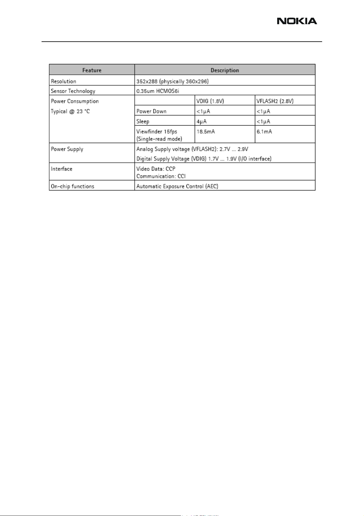
This section presents the electrical specifications of the GSM850/GSM1800/GSM1900
triple band transceiver, RH-26. The section contains electrical specifications, functional
descriptions and block diagrams. The RF requirements follow ETSI GSM850/GSM1800/
GSM1900 phase2+ specifications.
The module is supporting GPRS, EGPRS, and HSCSD protocols. GPRS multislot class in 10
and HSCSD multislot class is 6. EGPRS multislot classes are 1 - 2. Power class in
EGSM850 mode is 4 (33 dBm output power) and 1 in 1800/1900 bands (30 dBm). In 8PSK (EDGE) -mode power class is E2 (27 dBm in 850 band, and 26 dBm in 1800 and 1900
bands). Multislot power class in EGSM850 is 5 and in GSM1800/1900 bands 1.
The operating temperature range for all the components is from -10 to +80 C° unless
otherwise mentioned in the specifications.
The RF module performs the necessary high frequency operations of the GSM850/
GSM1800/GSM1900 triple band engine. Both the transmitter and receiver have been
implemented by using direct conversion architecture.
Another core component is a power amplifier module which includes two amplifier
chains, one for GSM850 and the other for GSM1800/GSM1900. Other key components
are a 26 MHz VCTCXO (voltage controlled temperature compensated crystal oscillator)
for frequency reference, 3420-3980 MHz SHF VCO (super high frequency voltage controlled oscillator), a front end module with a RX/TX switch with internal SAW filters
(EGSM850 and GSM1800), and one additional SAW filter and one balun for GSM1900
band. GSM850 and GSM1800 LNAs (low noise amplifier) for the receiver front-end are
integrated in Helgo, while GSM1900 LNA is external.
The control information for the RF is coming from the baseband section of the engine
through a serial bus, referred to later on as the RFBus. This serial bus is used to pass the
information about the frequency band, mode of operation, and synthesizer channel for
the RF. In addition, exact timing information and receiver gain settings are transferred
through the RFBus. Physically, the bus is located between the baseband ASIC called UPP
and Helgo. Using the information obtained from the UPP, Helgo controls itself to the
required mode of operation and further sends control signals to the front end and power
amplifier modules. In addition to the RFBus there are still other interface signals for the
power control loop and VCTCXO control and for the modulated waveforms.
The RF module takes care of all RF functions of the engine. RF circuitry is located on the
double side of the 8-layer PWB. PWB area for the RF circuitry is 8.7 cm2.
EMC leakage is prevented by using metal cans. The RF circuits are separated into three
blocks. The first includes the PA and TX 850band SAW. The second includes the front end
module, 1900 LNA and 1900 band SAW. The last block includes the Helgo RF IC, VCO,
VCTCXO and baluns. The RF transmission lines are made with striplines.
The RF transmission lines are made by striplines and microstriplines after PA.
Page 38 ©Nokia Corporation Issue 1 02/04
Page 39

RH-26
CCS Technical Documentation 2 - System Module
The baseband circuitry is located on the other side of the board, which is shielded with a
metallized frame and ground plane of the UI-board.
Maximum height of the RF components on the PWB is 1.8 mm. Heat generated by the
circuitry is carried off via the PWB ground planes and metallic shields.
Main technical specifications
Nominal and maximum ratings
Parameter Rating
Battery voltage nominal 3.7 V
Battery voltage maximum 4.2 V
Battery voltage minimum 3.1 V *)
Regulated supply voltage 2.78+/-3% V
*) Normal cut off battery voltage is 3.04V but minimum battery voltage level for RF is
2.95V.
RF frequency plan
The VCO operates at the channel frequency multiplied by two or four depending on the
frequency band of operation. This means that the baseband modulated signals are
directly converted up to the transmission frequency and the received RF signals directly
down to the baseband frequency. In addition, the circuit implementation of the frequency dividers in an integrated circuit offers a good topology for 90 degrees phase
shifter which is needed in the IQ-modulator and -demodulator.
Voltage reference 1.35+/-1.2% V
Operating temperature range
-10...+55 C
-25...+70 Co reduced performance,
no damage
o
Issue 1 02/04 ©Nokia Corporation Page 39
Page 40

RH-26
2 - System Module CCS Technical Documentation
Figure 21: RF frequency plan
DC characteristics
Regulators
The transceiver baseband section has a multi-function analogue ASIC, UEM, which contains six pieces of 2.78 V linear regulators and a 4.8 V switching regulator. All the regulators can be controlled individually by the 2.78 V logic directly or through a control
register. Normally, direct control is needed because of the switching speed requirement:
the regulators are used to enable the RF-functions which means that the controls must
be fast enough.
The use of regulators can be seen in the power distribution diagram. The seven regulators
are named from VR1 to VR7. VrefRF01 is used as the reference voltage for Helgo,
VrefRF01 (1.35V) for the bias reference.
The regulators (except for VR7) are connected to Helgo. Different modes of operation can
be selected inside Helgo according to the control information coming through the RFBus.
Page 40 ©Nokia Corporation Issue 1 02/04
Page 41

RH-26
CCS Technical Documentation 2 - System Module
Typical current consumption.
Operation mode Current consumption Notes
Power OFF < 10uA Leakage current (triple band PA)
RX, GSM850 75 mA, peak
RX, GSM 1800/GSM1900 70 mA, peak
TX, power level 5, GSM850 2500 mA, peak
TX, power level 0, GSM 1800/
GSM1900
1100 mA peak
Issue 1 02/04 ©Nokia Corporation Page 41
Page 42

RH-26
2 - System Module CCS Technical Documentation
Figure 22: Power distribution diagram
Helgo
Page 42 ©Nokia Corporation Issue 1 02/04
Page 43

RH-26
CCS Technical Documentation 2 - System Module
RF characteristics
Channel numbers and frequencies
Main RF characteristics
TX characteristics
Issue 1 02/04 ©Nokia Corporation Page 43
Page 44

RH-26
2 - System Module CCS Technical Documentation
RX characteristics
Table 24: Receiver characteristics
RF block diagram
The block diagram of the RF module can be seen in the figure below. The detailed functional description is given in the following sections.
Page 44 ©Nokia Corporation Issue 1 02/04
Page 45

RH-26
CCS Technical Documentation 2 - System Module
Figure 23: RF block diagram.
Helgo
Issue 1 02/04 ©Nokia Corporation Page 45
Page 46

RH-26
2 - System Module CCS Technical Documentation
Receiver
Each receiver path is a direct conversion linear receiver. From the antenna, the received
RF-signal is fed to a front end module where a diplexer first divides the signal into two
separate paths according to the band of operation: either lower, GSM850 or upper,
GSM1800/GSM1900 path. Each of the paths follows a pin-diode switch which is used to
select either a receive or transmit mode. At the upper band in the receive mode, either
GSM1800 or GSM1900 path is further selected by another pin-diode switch. The selections are controlled by Helgo, which obtains the mode/band and timing information
through the RFBus. After the front end module there is a SAW filter at each of the
receiver paths. Then, the signal is fed to the LNAs which are integrated in Helgo in
GSM850 and GSM1800 while in GSM1900 the LNA is external. In GSM1900 the amplified signal is fed to balun and after that to a pregain stage of the mixer, while in
GSM850 and GSM1800 the signals are connected directly to the LNA’s and after that to
the pregain stages. The pregain stages as well as all the following receiver blocks are
integrated in Helgo. The LNAs have three gain levels. The first one is the maximum gain,
the second one is about 30 dB below the maximum, and the last one is the off state
level.
After the pregain stages there are demodulator mixers at each signal path to convert the
RF signal directly down to baseband I and Q signals. Local oscillator signals for the mixers are generated by an external VCO. The frequency is divided by two in GSM1800 and
GSM1900 and by four in GSM850. Those frequency dividers are integrated in Helgo. They
provide accurate phase shifting by 90 degrees which is needed for the demodulator mixers.
The demodulator output signals are all differential. After the demodulators, there are
amplifiers called DtoS (differential to single ended) which convert those differential signals to single ended. Before that, they combine the signals from the three demodulators
to a single path which means that from the output of the demodulators to the baseband
interface there are just two signal paths (I and Q) which are common to all the frequency
bands of operation. In addition, the DtoS amplifiers perform the first part of the channel
filtering and AGC (automatic gain control): they have two gain stages, the first one with
a constant gain of 12 dB and 85 kHz -3 dB bandwidth and the second one with a switchable gain of 6 dB and -4 dB. The filters in the DtoS blocks are active RC filters. The rest of
the analogue channel filtering is provided by blocks called BIQUAD which include modified Sallen-Key biquad filters.
After the DtoS and BIQUAD blocks there is another AGC-amplifier which provides a gain
control range of 42 dB in 6 dB steps.
In addition to the AGC steps, the last AGC stage also performs the real time DC offset
compensation which is needed in a direct conversion receiver to cancel out the effect of
the local oscillator leakage. DC offset compensation is performed during the operations
called DCN1. DCN1 is carried out by charging large off-chip capacitors in the last AGC
stages to a voltage which causes a zero DC offset.
After the last AGC and DC offset compensation stages, the single ended and filtered Iand Q-signals are finally fed to the RX ADCs. The maximum peak-to-peak voltage swing
Page 46 ©Nokia Corporation Issue 1 02/04
Page 47

RH-26
CCS Technical Documentation 2 - System Module
for the ADCs is 1.45 V.
Transmitter
In contrast to the receiver where the adaptation to the modulation (GMSK) is performed
by the DSP algorithm, the transmitter must be configured differently also as regards the
hardware. The selected modulation scheme affects the operation of the IQ-modulator,
power control loop, and the power amplifier biasing.
Generally, the transmitter consists of two final frequency IQ-modulators and power
amplifiers, for the lower and upper bands separately, and a power control loop. The IQmodulators are integrated in Helgo, as well as the operational amplifiers of the power
control loop. The two power amplifiers are located in a single module and the power
detector, directional coupler, and loop filter parts of the power control loop are implemented as discrete components on the PCB. In the GMSK mode, the power is controlled
by adjusting the DC bias levels of the power amplifiers.
The modulated waveforms, the I- and Q-signals, are generated by the baseband part of
the engine module. After postfiltering, implemented as RC-networks, waveforms are
transferred into the IQ-modulator. Local oscillator signals for the modulator mixers are
generated by an external VCO the frequency of which is divided by two in GSM1800 and
in GSM1900 and by four in GSM850. Those frequency dividers are integrated in Helgo
and in addition to the division they also provide accurate phase shifting by 90 degrees
which is needed for the modulator mixers.
At the upper band there is a dual mode buffer amplifier at the output of the IQ-modulator. In the GMSK mode it acts as a buffer amplifier while in the 8-PSK mode it is used as
a voltage variable attenuator.
The final amplification is realised by a three stage power amplifier. There are two different amplifier chains in a single amplifier module, one for GSM850 and one for
GSM1800/GSM1900. The lower band power amplifier is able to deliver over 2 W of RF
power, while the capability of the upper band amplifier is over 1 W. In the GMSK mode,
the gain control is implemented by adjusting the bias voltages of the first two transistor
stages, reaching the dynamic range of over 70 dB. In the 8-PSK mode, the biases are
fixed and they are set higher than in the GMSK mode to meet the more demanding linearity requirements.
After the power amplifier, the signal goes through a low pass filter and a pin-diode
switch which is used to select between the reception and transmission. Finally, the two
signal paths, lower and upper band, are combined in a diplexer after which the signal is
routed through an antenna connector to the antenna.
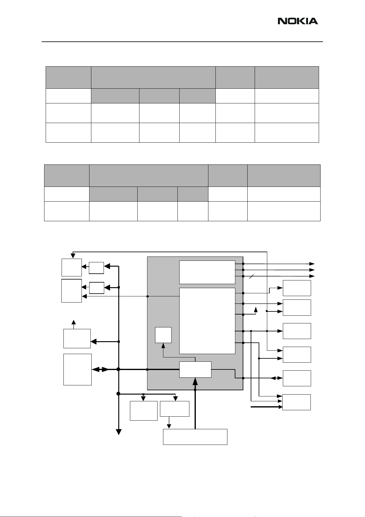
Connections
Antenna
The GSM850/GSM1800/GSM1900 transceiver uses internal antenna.
Issue 1 02/04 ©Nokia Corporation Page 47
Page 48

RH-26
2 - System Module CCS Technical Documentation
RF-BB interface
Figure 24: Engine block diagram
Page 48 ©Nokia Corporation Issue 1 02/04
 Loading...