

Page 1

CCS Technical Documentation
RH-26 Series Transceivers
7 - Troubleshooting Instructions
Issue 1 02/04 ©Nokia Corporation
Page 2
RH-26
7 - Troubleshooting Instructions CCS Technical Documentation
[This page left intentionally blank]
Page 2 ©Nokia Corporation Issue 1 02/04
Page 3

RH-26
CCS Technical Documentation 7 - Troubleshooting Instructions
Table of Contents
Page No
RF Troubleshooting ....................................................................................................... 4
RF key component placement .....................................................................................6
RF measurement points ...............................................................................................7
GSM850, GSM1800 and GSM1900 Transmitter ........................................................9
General instructions for Tx troubleshooting ............................................................. 9
Transmitter troubleshooting diagram ........................................................................10
PA/antenna switch troubleshooting diagram .............................................................11
Pictures of transmitter signals ....................................................................................12
Additional Information for EDGE troubleshooting..................................................... 14
Transmitter EDGE troubleshooting diagram .............................................................15
PA & antenna switch EDGE troubleshooting diagram .............................................16
Pictures of EDGE transmitter signals ........................................................................17
GSM850, GSM1800 and GSM1900 Receiver............................................................. 18
General instructions for Rx troubleshooting ..............................................................18
Troubleshooting diagram for GSM850 receiver ........................................................20
Troubleshooting diagram for GSM1800 receiver ......................................................21
Troubleshooting diagram for GSM 1900 receiver .....................................................22
Synthesizer................................................................................................................... 23
General instructions for synthesizer troubleshooting ................................................23
Synthesizer troubleshooting diagram ........................................................................24
Pictures of synthesizer signals ...................................................................................25
Baseband Troubleshooting........................................................................................... 26
Faults by symptom .....................................................................................................28
SIM card.................................................................................................................. 28
Display .................................................................................................................... 29
Keypad .................................................................................................................... 30
Lights....................................................................................................................... 32
Charging.................................................................................................................. 34
Pop-PortTM system connector................................................................................ 34
Audio....................................................................................................................... 37
Vibra........................................................................................................................ 41
Real time clock battery............................................................................................ 41
Flip position recognition ......................................................................................... 41
IR............................................................................................................................. 42
Bluetooth................................................................................................................. 42
Camera .................................................................................................................... 43
Baseband calibration ..................................................................................................45
Issue 1 02/04 ©Nokia Corporation Page 3
Page 4

RH-26
7 - Troubleshooting Instructions CCS Technical Documentation
[This page intentionally blank]
Page 4 ©Nokia Corporation Issue 1 02/04
Page 5

RH-26
CCS Technical Documentation 7 - Troubleshooting Instructions
RF Troubleshooting
Measurements should be done using a spectrum analyzer with a high-frequency highimpedance passive probe (LO-/reference frequencies and RF power levels) and an oscilloscope with a 10:1 probe (DC-voltages and low frequency signals)
The RF-section is build around one RF-ASIC (HELGO N500).
Most RF semiconductors are static discharge sensitive! So ESD protection must be
taken care of during repair (ground straps and ESD soldering irons).
Apart from key components described in this document there are a lot of discrete components (resistors, inductors and capacitors). Their troubleshooting is done by checking
that the soldering of the component is done properly (for factory repairs checking if it is
missing from the PWB). Capacitor can be checked for shortening and resistors for value
by means of an ohmmeter, but be aware, in-circuit measurements should be evaluated
carefully.
Please be note that all measured voltages or RF levels in this document are rough figures.
Especially RF levels vary due to different measuring equipment and different grounding
of the probe used. When using the RF probe, use metallic tweezers to connect the probe
ground to the PWB ground as close to measurement point as possible.
Issue 1 02/04 ©Nokia Corporation Page 5
Page 6
RH-26
7 - Troubleshooting Instructions CCS Technical Documentation
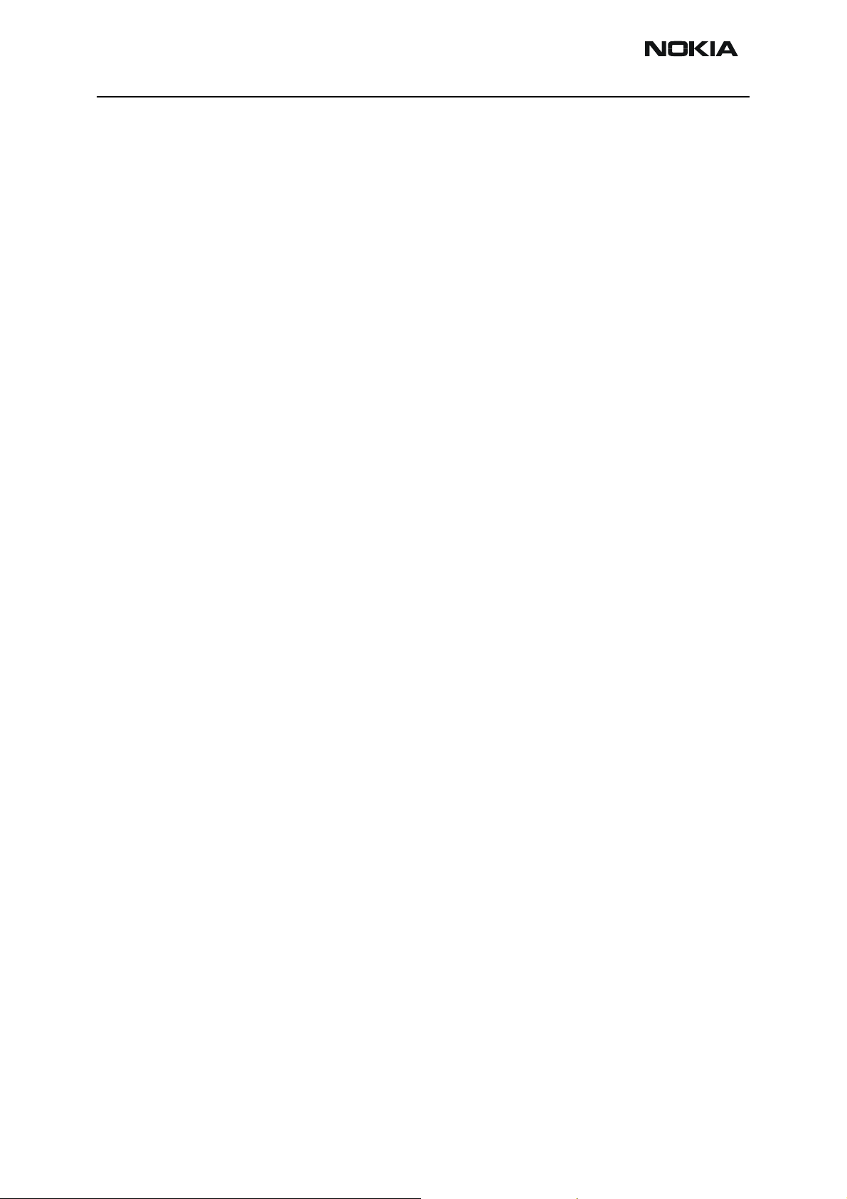
RF key component placement
Figure 1: RF key component placement - top side
Page 6 ©Nokia Corporation Issue 1 02/04
Page 7
RH-26
CCS Technical Documentation 7 - Troubleshooting Instructions
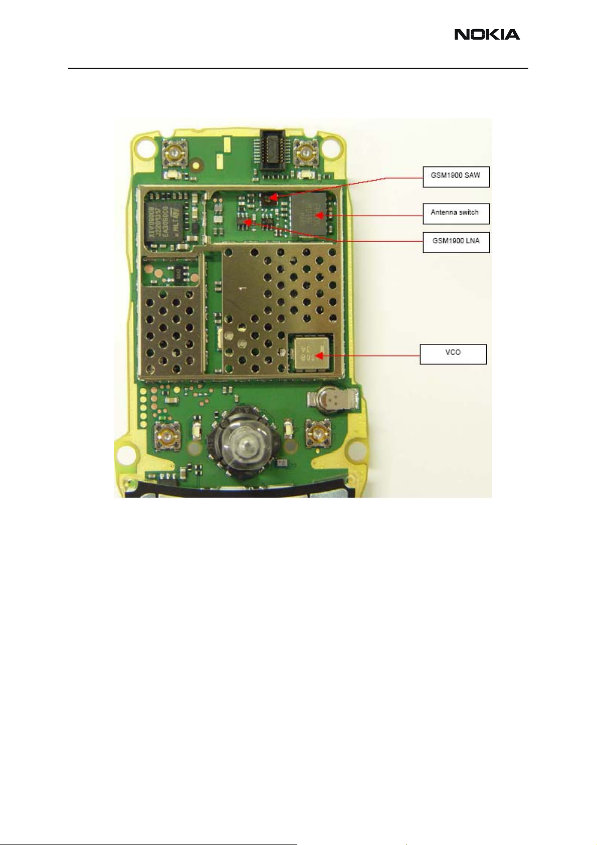
RF measurement points
Figure 2: RF measurement points - top side
Issue 1 02/04 ©Nokia Corporation Page 7
Page 8
RH-26
7 - Troubleshooting Instructions CCS Technical Documentation
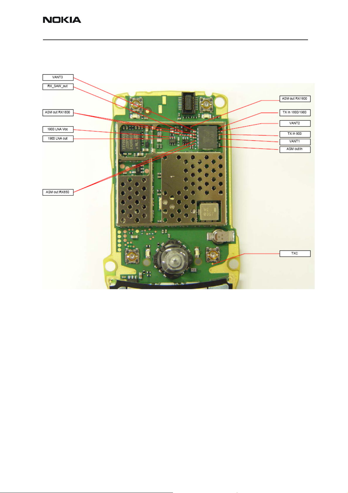
Figure 3: RF measurement points - bottom side
Page 8 ©Nokia Corporation Issue 1 02/04
Page 9

RH-26
CCS Technical Documentation 7 - Troubleshooting Instructions
GSM850, GSM1800 and GSM1900 Transmitter
General instructions for Tx troubleshooting
1 Connect test jig to computer with DAU-9S cable or to FPS-8 flash prommer with
XCS-4 modular cable.
Make sure that you have PKD-1 dongle connected to computers parallel port.
2 Connect DC power supply to module test jig with FLC-2 cable.
Note: When repairing or tuning transmitter use external DC supply with at
least 3A current capability. Set the DC supply voltage to 4.2V.
3 Connect an RF cable to the module test jig (MJ-5), RF connector to measurement
equipment or at least 10dB attenuator, otherwise the PA may be damaged. Normally a spectrum analyzer is used as measurement equipment.
Note: Normally spectrum analyzer maximum input power is +30dBm. It is recommended to use 10dB attenuator in spectrum analyzer input to prevent damage.
4 Set the phone module to test jig and start Phoenix service software.
5 To initialize connection to the phone (when using FPS-8 together with DAU-9S
and COMBOX driver, use FBUS driver):
• From the File menu, choose Product.
• Select RH-26.
• From the toolbar, set operating mode to "Local".
6 To activate the RF controls window:
From the Testing menu, choose RF Controls
7 In the RF controls window:
• Select band "GSM850", "GSM 1800" or “GSM1900 (Default = "GSM850").
• Set Active unit to "Tx" (Default = "Rx").
• Set Operation mode to "Burst" (Default = "Burst").
• Set Tx data type to "Random" (Default = "All1").
• Set Rx/Tx channel to 37 on GSM850 band or 700 on GSM1800 band or 661 on
GSM1900 (Defaults).
Issue 1 02/04 ©Nokia Corporation Page 9
Page 10
RH-26
7 - Troubleshooting Instructions CCS Technical Documentation
• Set Tx PA mode to "Free" (Default).
• Set power level to 5 (Default = 19) on GSM850 or to 0 (Default = 15) on
GSM1800 and GSM1900.
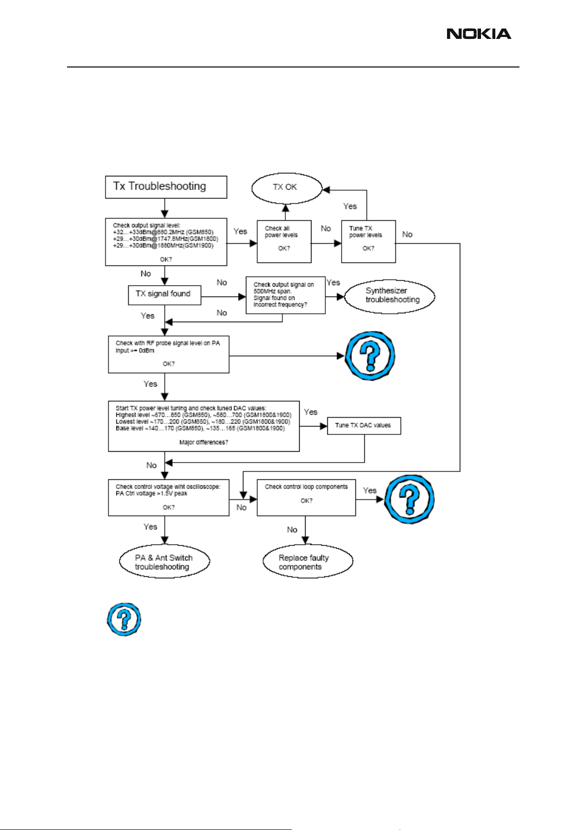
Transmitter troubleshooting diagram
= beyond economical repair
Page 10 ©Nokia Corporation Issue 1 02/04
Page 11
RH-26
CCS Technical Documentation 7 - Troubleshooting Instructions
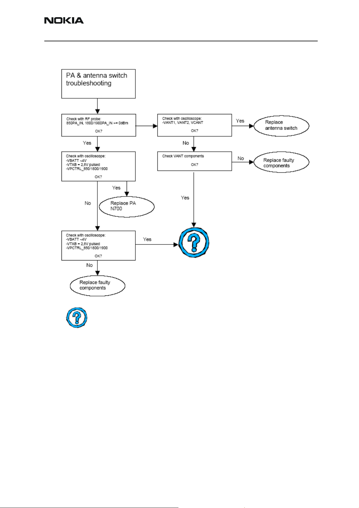
PA/antenna switch troubleshooting diagram
= beyond economical repair
Issue 1 02/04 ©Nokia Corporation Page 11
Page 12
RH-26
7 - Troubleshooting Instructions CCS Technical Documentation
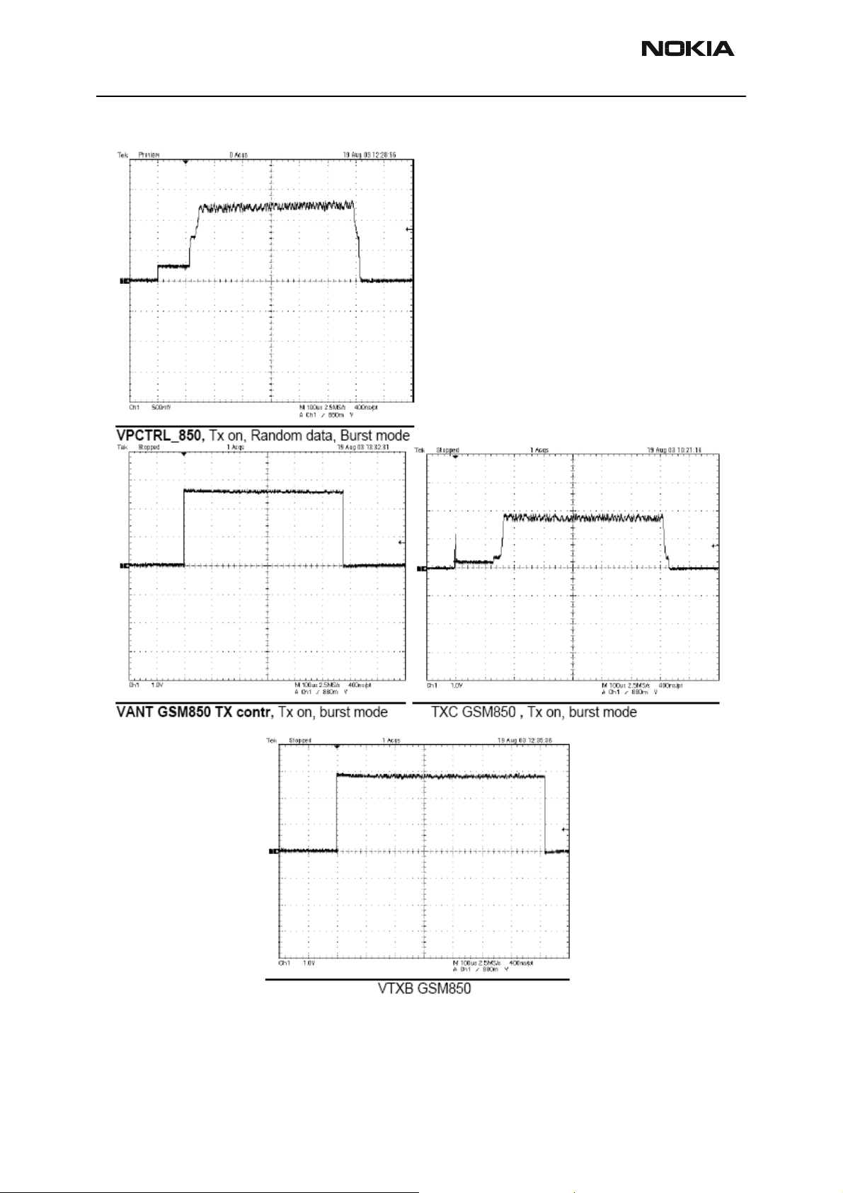
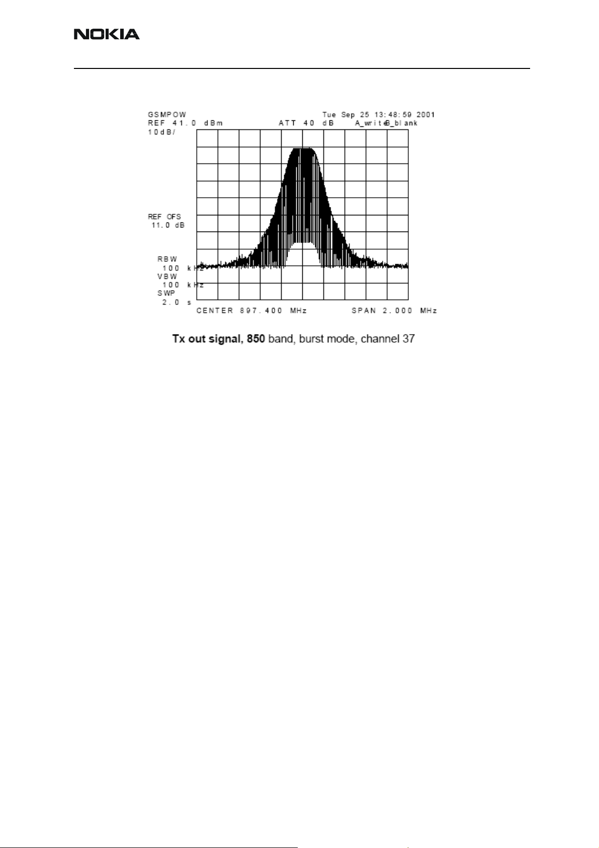
Pictures of transmitter signals
Page 12 ©Nokia Corporation Issue 1 02/04
Page 13
RH-26
CCS Technical Documentation 7 - Troubleshooting Instructions
Issue 1 02/04 ©Nokia Corporation Page 13
Page 14
RH-26
7 - Troubleshooting Instructions CCS Technical Documentation
Additional Information for EDGE troubleshooting
Note! EDGE mode troubleshooting differs slightly from basic GSM troubleshooting.
1 Establish connection to the phone normally (see GSM850/GSM1800/GSM1900
troubleshooting instructions).
2 From the File menu, choose Product.
3 Select RH-26.
4 From the toolbar, set operating mode to “Local”.
5 To activate the RF Controls window:
• From the Testing menu, choose RF Controls.
6 In the RF Controls window:
• Select Band “GSM850”, “GSM1800” or “GSM1900” (Default = “GSM850”).
• Set Active unit to “Tx” (Default “Rx”).
• Set Edge “On” (Default = “Off”).
• Set Operation mode to “Burst” (Default = “Burst”).
• Set Tx data type to “Alternate PN9” (Default = “All 1”).
• Set Rx/Tx channel to 37 on GSM850, 700 on GSM1800 or 661 on GSM1900
(Defaults).
• Set Power level to 8 on GSM850 (Default = “19”) or to 2 on GSM1800 and
GSM1900 (Default = “15”).
NOTE! For GSM850 EDGE power levels 5, 6 and 7 are not in use and for GSM1800 and GSM1900
EDGE power levels 0 and 1 are not in use.
Page 14 ©Nokia Corporation Issue 1 02/04
Page 15

RH-26
CCS Technical Documentation 7 - Troubleshooting Instructions
Transmitter EDGE troubleshooting diagram
= beyond economical repair
Issue 1 02/04 ©Nokia Corporation Page 15
Page 16

RH-26
7 - Troubleshooting Instructions CCS Technical Documentation
PA & antenna switch EDGE troubleshooting diagram
= beyond economical repair
Page 16 ©Nokia Corporation Issue 1 02/04
Page 17

RH-26
CCS Technical Documentation 7 - Troubleshooting Instructions
Pictures of EDGE transmitter signals
Issue 1 02/04 ©Nokia Corporation Page 17
Page 18

RH-26
7 - Troubleshooting Instructions CCS Technical Documentation
GSM850, GSM1800 and GSM1900 Receiver
General instructions for Rx troubleshooting
1 Connect test jig to computer with DAU-9S cable or to FPS-8 Flash Prommer with
XCS-4 modular cable.
Make sure that you have PKD-1 dongle connected to computers parallel port.
2 Connect DC power supply to module test jig with FLC-2 cable.
3 Set the DC supply voltage to 4.2V.
4 Connect an RF-cable to the module test jig (MJ-5) RF connector and to RF signal
generator.
5 Set the phone module to test jig and start Phoenix service software.
6 To initialize connection to the phone (use FBUS driver when using DAU-9S and
COMBOX driver when using FPS-8).
• From the File menu, choose Product.
• From the list, select RH-26.
• From toolbar set operating mode to "Local"
7 To activate the RF controls window:
• From the Testing menu, choose RF Controls.
8 In the RF controls window:
• Select band "GSM850", "GSM1800" or “GSM1900” (Default = "GSM850").
• Set Active unit to "Rx" (Default = "Rx").
• Set Operation mode to "Continuous" (Default = "Burst").
• Set AGC to "12: FEG_ON + DTOS_ON + BB_30 = Vgain_60” (Default = "12:
FEG_ON + DTOS_ON + BB_42 = Vgain_72").
• Set Rx/Tx channel to 37 on GSM850 band, 700 on GSM1800 band or 661 on
GSM1900 (Defaults).
• Apply 942.46771 MHz (channel 37 + 67.710 kHz offset), 1842.86771 MHz (channel 700 + 67.710 kHz offset) or 1960.06771 MHz (channel 661 + 66.710 kHz offset) –90 dBm signal to the RF-connector (remember to compensate for cable
attenuation).
Page 18 ©Nokia Corporation Issue 1 02/04
Page 19

RH-26
CCS Technical Documentation 7 - Troubleshooting Instructions
When measured with an oscilloscope on "RX_I" or "RX_Q", the following screens
should be seen on a working GSM850, GSM1800 or GSM1900 receiver:
9 Correct signal amplitudes approximately:
• GSM850~190mVpp
• GSM1800~140mVpp
• GSM1900~160mVpp
Signal part frequency 67,7110 kHz sine.
DC level of signal part is 1,30V. DC level can variate about +/- 100mV between I
and Q signals and between different bands as well.
View of GSM1900 continuous mode RX I and Q signals measured from test points
RXI and RXQ simultaneously.
Issue 1 02/04 ©Nokia Corporation Page 19
Page 20

RH-26
7 - Troubleshooting Instructions CCS Technical Documentation
Used channel 37 input signal 942,46771 MHz, level –90 dBm at antenna port,
AGC setting 12.
Phase difference should be 90 degrees between I and Q signals at all bands.
Troubleshooting diagram for GSM850 receiver
= beyond economical repair
Page 20 ©Nokia Corporation Issue 1 02/04
Page 21

RH-26
CCS Technical Documentation 7 - Troubleshooting Instructions
Troubleshooting diagram for GSM1800 receiver
= beyond economical repair
Issue 1 02/04 ©Nokia Corporation Page 21
Page 22

RH-26
7 - Troubleshooting Instructions CCS Technical Documentation
Troubleshooting diagram for GSM 1900 receiver
= beyond economical repair
Page 22 ©Nokia Corporation Issue 1 02/04
Page 23

RH-26
CCS Technical Documentation 7 - Troubleshooting Instructions
Synthesizer
General instructions for synthesizer troubleshooting
1 Connect test jig to computer with DAU-9S cable or to FPS-8 Flash Prommer with
XCS-4 modular cable.
Make sure that you have PKD-1 dongle connected to computers parallel port.
2 Connect DC power supply or FPS-8 to module test jig with FLC-2 cable.
3 Set the DC supply voltage to 4.2V.
4 Set the phone module to test jig and start Phoenix service software.
5 To initialize connection to the phone (use FBUS driver when using DAU-9S and
COMBOX driver when using FPS-8):
• From the File menu, choose Product.
• Select RH-26.
6 From the toolbar, set operating mode to "Local".
7 To activate the RF controls window:
• From the Testing menu, choose RF Controls.
8 In the RF Controls window:
• Select band "GSM850", "GSM 1800" or “GSM 1900” (Default = "GSM850")
• Set Active unit to "Rx" (Default = "Rx")
• Set Operation mode to "Continuous" (Default = "Burst")
• Set Rx/Tx channel to 37 on GSM850 band, 700 on GSM1800 band or 661 on
GSM1900 band (Defaults)
Issue 1 02/04 ©Nokia Corporation Page 23
Page 24

RH-26
7 - Troubleshooting Instructions CCS Technical Documentation
Synthesizer troubleshooting diagram
= beyond economical repair
Page 24 ©Nokia Corporation Issue 1 02/04
Page 25

RH-26
CCS Technical Documentation 7 - Troubleshooting Instructions
Pictures of synthesizer signals
Issue 1 02/04 ©Nokia Corporation Page 25
Page 26

RH-26
7 - Troubleshooting Instructions CCS Technical Documentation
Baseband Troubleshooting
These instructions show how to repair the baseband section of RH-26 transceiver. Since
RH-26 transceiver shielding is made by using fixed shielding cans, there are some limitations for servicing work (see relevant service bulletins for more information). This is due
to fact that when soldering new cans, component joints located under the shielding cans
may be damaged. Also as a result, traditional troubleshooting flow chart is not very practical in the case of RH-26. Instead, fault cases are handled by fault symptoms.
NOTE:
• Inside the flip unit there are no serviceable parts either, the whole unit should be
replaced in fault situation.
• Appropriate service tools and Phoenix service software are needed for troubleshooting.
• Camera module is very sensitive to heat and must be always removed when
doing solderings to main board.
Figure 4: Transceiver module - top view
Page 26 ©Nokia Corporation Issue 1 02/04
Page 27

RH-26
CCS Technical Documentation 7 - Troubleshooting Instructions
Figure 5: Transceiver module - bottom view
Issue 1 02/04 ©Nokia Corporation Page 27
Page 28

RH-26
7 - Troubleshooting Instructions CCS Technical Documentation
Faults by symptom
SIM card
The whole SIM interface locates in two chips: UPP and UEM. The SIM card is connected
to UEM through EMI/ESD filter R388. The SIM card detection signal is taken from the BSI
line. If the “Insert SIM card” text or other SIM related message appears on the display,
check the following:
• BSI contact is reliable. Very short break can cause “Insert SIM card” message.Typical DC-level is 1.19V with BL-5C.
• SIM connector contacts and solderings. SIM card holder.
VSIM,SIM CLK,SIM RST and SIM DATA signals are according to the figure below after the
power switched on. If signals are OK only at test points, change R388. Note that SIM
connector contacts are on the opposite side of the connector pads
Figure 6: SIM test points.
Page 28 ©Nokia Corporation Issue 1 02/04
Page 29

RH-26
CCS Technical Documentation 7 - Troubleshooting Instructions
Figure 7: SIM signals at start-up with 3V SIM card
Display
Display is a 130 * 130 dot LCD display with 4096 colors.The illumination is accomplished
with 3 LEDs integrated into the LCD module as well as the display drivers mounted on
the flex. Serial data transfer begins when UPP drives the CSX pin low and starts by setting bits to SDA. The bits are read by the display on the rising edge of SCLK. RESX
GENIO(4) line is normally 1.8 V.
There are no serviceable components in the LCD module, the whole module must be
changed in fault situation.
If change does not help, check:
1 Signals at test points should be like in Figure: LCD Signals.
2 Series resistors R301,R302 and R303.
3 Connector contacts and solderings.
Figure 8: LCD test points.
Issue 1 02/04 ©Nokia Corporation Page 29
Page 30

RH-26
7 - Troubleshooting Instructions CCS Technical Documentation
Figure 9: LCD signals
Figure 10: Location of LCD-related components
Keypad
RH-26 phone includes traditional T9 and qwerty keypads. The keys on the engine board
are connected through EMI/ESD filter Z300 (under UPP shielding can) to the KEYB(10:0)
bus to the UPP. Volume up/down functionality is combined with joystick functionality.
Two of the KEYB(10:0) lines are connected through EMI/ESD filter Z301 to the joystick.
Engine keypad includes half of the qwerty, PWR and “soft” keys. 5-way joystick is used
for navigation. The power on key is connected to the UEMK PWRONX signal and is not
part of the keypad matrix.
The flip keypad includes T9 and second half of the qwerty keys. SEND & END keys are on
the flip module. Keypad matrix is connected to the MCU located on the flip PWB. Key
presses are sent to UPP through flip interface. This interface consist of VBAT, DATA, CLK
and GND lines. GND connection is made through connector shielding and others with 3
flexible micro-coax cables, all included in one plug.
Page 30 ©Nokia Corporation Issue 1 02/04
Page 31

RH-26
CCS Technical Documentation 7 - Troubleshooting Instructions
Symptoms
Flip does not work:
• Check that flip connector contacts are reliable. Connector is properly assembled
when clear snap can be heard when pressing it down.
• Check DATA- and CLK-signals, see figures: Flip Test points and Flip CLK and Data.
• Series coils L300,L301,L302 and VBAT, see Figure: Flip Test Points.
• VBAT switch V320 is under UPP shielding and is always on when power is turned
on.
If one key does not work, check mechanical damages or dirt under qwerty keydomes.
Power switch is connected to UEM through resistor R306.
Joystick does not work. There may be a mechanical damage or EMI/ESD filter Z301 is
broken.
If several keys are not working, it means that at least one of the KEYB(10:0) lines is broken. In this case, repair is not possible.
If one qwerty or T9 key is stuck down, the corresponding keypad does not work.
Figure 11: Flip test points
Figure 12: Flip CLK and data
Issue 1 02/04 ©Nokia Corporation Page 31
Page 32

RH-26
7 - Troubleshooting Instructions CCS Technical Documentation
Lights
The total amount of LEDs is 19 pcs: 3 inside LCD, 8 assembled to engine and 8 to flip
module. LCD and engine LEDs are powered from DC-DC converter D300 located under
the UPP shielding. LCD and function keys are always illuminated when D300 is switched
on. On/off control line is UIDRV(3) KLight. Engine side qwerty-LEDs have own switch
V350 controlled by UIDRV(2) DLight line. Both controls are driven by UEMK D200.
Flip LEDs are connected straight to VBAT. Both T9 and qwerty lights have own switch and
can be independently switch on and off by flip MCU.
Symptoms
No lights.
• Engine side (half-qwerty, function keys and LCD). D300 circuitry under UPP
shielding is faulty. Repair is not possible.
One or more LED blank.
• Check all LEDs and series resistors R311, R312, R313 and R314. If the engine side
qwerty-LEDs V311-V314 are blank, check switch V350, which is located under the
UEM shielding. Lights are on when DLight line (R305) is 1.8V.
Illumination failure LCD.
• Check LCD connector X300/pins 1,2. If OK, change LCD module.
Illumination failure flip, keyboard working.
• Change flip module.
Figure 13: Engine LEDs and series resistors
Page 32 ©Nokia Corporation Issue 1 02/04
Page 33

RH-26
CCS Technical Documentation 7 - Troubleshooting Instructions
Figure 14: Engine LEDs and series resistors
Issue 1 02/04 ©Nokia Corporation Page 33
Page 34

RH-26
7 - Troubleshooting Instructions CCS Technical Documentation
Charging
Charging is controlled by UEMK D200 and software. Two charger connectors are used:
one in the system connector soldered to the PWB and one spring contact to DC-jack in
the B-cover assy.
If charging does not work, check:
• DC-jack X102 spring contacts and system connector X101 solderings.
• BTemp resistor R105. Typical voltage at +25°C is 0.9V.
• Charging circuitry external components; fuse F100, coil L100 and protection
diode V100.
• If these are OK, UEM circuitry is faulty. The circuitry consists of UEMK D200 itself
and series resistor R200.
Pop-PortTM system connector
System connector X101 has the following interfaces:
Figure 15: Charging circuitry components.
• Pads for 2 -wire charging in cradles.
• 2-wire fully differential mono audio output.
• 2-wire differential microphone input.
• 2.78V 70 mA output to accessories.
Page 34 ©Nokia Corporation Issue 1 02/04
Page 35

RH-26
NC N
CCS Technical Documentation 7 - Troubleshooting Instructions
• ACI accessory detection/removal & controlling.
• Standard FBUS.
All lines are connected to engine through series components and if the connector itself
and solderings are OK, check those components.
If Vout voltage to accessories is missing, check regulator N100 located under the UEM
shielding. Vout 2.78V is switched on when GENIO(0) is 1.8V.
Figure 16: Pop-PortTM system connector
C
Shielding GND HSEAR R P
HSEAR P
HSEAR N
HSEAR R N
XMIC P
XMIC N
Fbus RX
Fbus TX
ACI
Charge GND
Shielding
GND
Vout
Charge
114
Issue 1 02/04 ©Nokia Corporation Page 35
Page 36

RH-26
7 - Troubleshooting Instructions CCS Technical Documentation
Table 1: System connector interface description
Pin # Signal Notes
1 VCHAR Charging voltage input
2 GND Charge ground
3 ACI Accessory insertion & removal detection /
Serial data bi-directional 1 kbit/s. Pull-up to
2.78V when no accessories connected.
4 Vout 2.8V supply for ACI accessories. 0V when no
accessories present.
5 Not used
6 FBUS_RX Serial data from accessory to phone /
115 kb it /s
7 FBUS_TX Serial data from phone to accessory /
115 kb it /s
8 GND Data ground
9 XMIC N Negative audio in signal
10 XMIC P Positive audio in signal. 2.1V bias for microphone
when ext. mic. in use.
11 HSEAR N Negative audio out signal.
12 HSEAR P Positive audio out signal.
13 Not used, connected to GND
14 Not used, connected to GND
Figure 17: ACI regulator N100
Page 36 ©Nokia Corporation Issue 1 02/04
Page 37

RH-26
CCS Technical Documentation 7 - Troubleshooting Instructions
Figure 18: System connector series components
Audio
The audio hardware is mostly integrated into the UEMK D200. External amplifier N150 is
needed to drive the internal handsfree speaker (IHF). Other external components are
functioning as capacitors, series resistors and ESD protection components. The required
bias voltages for internal and external microphones are also taken from the UEMK.
Acoustics components are assembled into the phone mechanics. All contacts are spring
type, so in fault situation check that pads on the PWB are clean and spring force is OK.
Earpiece is fed by the differential signals "EARP" and "EARN" from the UEMK. External
earpiece signals is fed by the "HF" & "HFCM" pins.
MIC1N & MIC1P (audio signals) and MICB1 (bias voltage) are used for the internal
microphone. MIC2N & MIC2P and MICB2 are used for external microphone.
IHF circuitry uses XAUDIO(7) output from the UEMK for normal voice. For ringing and
alert tones, which should be heard simultaneously from the headset and IHF speaker, differential output (HF&HFCM) from the UEMK is used. The shutdown of the IHF amplifier is
controlled by the UPP using GENIO(13).
Furthermore, a couple of signals are needed to control the external audio device. HEADINT signal is needed for recognising an external device (e.g. headset) connected to the
system. The recognition is based on the ACI-in on the system connector that is sorted to
ground inside the external device used. HOOKINT is generated by a button of an external
device.
Issue 1 02/04 ©Nokia Corporation Page 37
Page 38

RH-26
7 - Troubleshooting Instructions CCS Technical Documentation
Symptoms
No voice from earpiece or bad quality.
• Earpiece is integrated into LCD module and the whole module must be changed
in fault situation. If change does not help, check L150 under RF-shield assembly
and R160 under the UEMK shielding.
No voice from microphone or bad quality.
• Microphone is in B-cover assembly and it is a replaceable part. Needed bias for
microphone is 2.1V, which is fed from AUDIO(4) MICB1 line through R165. Series
components are C153 and R157.
No voice from IHF speaker or bad quality.
• Check IHF amplifier N150 output series components L151 and L152. IHF speaker
is integrated into antenna and the whole antenna module must be changed in
fault situation. If change does not help, failure is under the UEMK shielding.
Input lines for the IHF amplifier are XAUDIO(7), XAUDIO(1) HF and XAUDIO(2)
HFCM. XAUDIO(7) series components are C170 and R169. HF and HFCM signals
are fed through C158, C166 and R164. Control line for the IHF amplifier is
GENIO(13), which is 1.8V when the amplifier is on.
External audios does not work.
• Refer to the previous section Pop-PortTM system connector. EXTMIC series components are C154 and R155. The required bias for the external microphone is
2.1V, which is fed from XAUDIO(3) MICB2 line through R156 and R153. XEAR
series component is R162. HOOKINT information goes through R166 to the UEMK
and HEADINT through R102.
Page 38 ©Nokia Corporation Issue 1 02/04
Page 39

RH-26
CCS Technical Documentation 7 - Troubleshooting Instructions
Figure 19: Location of audio components
Figure 20: Location of earpiece-related test points
Figure 21: Location of IHF-related test points
Issue 1 02/04 ©Nokia Corporation Page 39
Page 40

RH-26
7 - Troubleshooting Instructions CCS Technical Documentation
Figure 22: Location of microphone pads
Page 40 ©Nokia Corporation Issue 1 02/04
Page 41

RH-26
CCS Technical Documentation 7 - Troubleshooting Instructions
Vibra
Vibra motor M100 is soldered directly to the PWB and it is controlled by a PWM signal
(UEM UIDRV (1) line). The other vibra pad is connected straight to VBat. If the vibra does
not work, the possible fault is located in the vibra motor itself or in the UEM circuitry.
Figure 23: Location of vibra motor
Real time clock battery
Regulator for charging back-up battery G300 is inside the UEM. Charging starts when
the main battery is connected and power is on.
The battery type is cell capacitor and it is soldered directly to the PWB. Typical voltage
for a fully charged battery is 3.2V, but backup circuitry can operate between 2-3.3V. If
RTC does not work, the possible fault is in the RTC battery itself or in the UEM circuitry.
Figure 24: Location of RTC battery
Flip position recognition
The flip position, open or close, is detected by the hall sensor N301. The hall sensor
detects the magnet, which is integrated into the flip mechanics.
Issue 1 02/04 ©Nokia Corporation Page 41
Page 42

RH-26
7 - Troubleshooting Instructions CCS Technical Documentation
Hall sensor output is 2.78V when the flip is closed, 0V when open. Output is connected
to the UEM via SLOWAD(2) KEYB1 line.
If the flip is not recognised, check:
• N301/pin 3 output = 0V.
• N301/pin 1 = 2.78V. If not check R309.
• Bring the magnet close.
• If the pin 3 does not go up, change the Hall sensor N301.
Figure 25: Location of hall sensor
IR
The infrared module N350 is connected to the UPP through IACCDID(0,1) line and
GENIO(24) line. TxD and SD are active when high, while RxD is active when low. All IR
related components are under the UPP shielding except the IR module itself.
Bluetooth
Figure 26: IR Signals
All bluetooth functions are integrated into a single chip, only a few external components
Page 42 ©Nokia Corporation Issue 1 02/04
Page 43

RH-26
CCS Technical Documentation 7 - Troubleshooting Instructions
are needed (RF filters, power supply filtering, etc.) Bluetooth components are under the
RF shield assembly. External 2.8V regulator N131 is used as a power supply for bluetooth
internal regulator, which is switched on by PURX line. Antenna is integrated into the
main PWB, same shape in all layers 1-8.
In fault situation check:
• There is no mechanical damage between test point J148 and antenna.
• Output of N131 (VREG_IN) is 2.8V at test point J130. If not, check control signal
PURX 1.8V at N131/pin3 and Vbat at N131/pin1. If OK, change N131.
Figure 27: Bluetooth test points
Camera
Camera is connected to baseband (UPP) through HW accelerator IC D970. External 1.8V
regulator N970 is used as a power supply (VCAMDIG) for camera module and for HW
accelerator together with VFLASH2. N970 is switched on and off by GENIO(1) line.
In fault situation:
• Remove camera module and check connector X970 contacts and solderings.
• Check regulator N970: output should be 1.8V at C983,984 when J974 is 1.8V.
• Signals are according to the attached figures below:
Issue 1 02/04 ©Nokia Corporation Page 43
Page 44

RH-26
7 - Troubleshooting Instructions CCS Technical Documentation
Figure 28: Camera test points
Figure 29: Camera signals
Page 44 ©Nokia Corporation Issue 1 02/04
Page 45

RH-26
CCS Technical Documentation 7 - Troubleshooting Instructions
Baseband calibration
All these calibrations should be performed by using the JBV-1 box, controlled by Phoenix
through FPS-8. Calibration is done in the LOCAL mode.
Manual calibration instructions:
1 Calibrate VBAT.
• Set VBATT line to 3.1V and 4.2V (+/-20 mV) -> read AD-converter values and
save them.
• VBAT calibration is made in order to get correct battery voltage.
2 Calibrate BSI.
• Set to BSI line 1% 75kohm resistor -> read AD-converter value and save it.
• BSI calibration is made in order to get correct battery size information.
3 Calibrate VCHARGE.
• Connect 8.4V (+/-20 mV) to charger line -> read AD-converter value and save it.
• VCHARGE calibration is made in order to get charger types and charger voltages
correct.
4 Calibrate charging current.
• Connect 500mA (+/-15 mA) to charger line -> read AD-converter value and save
it.
• Charging current calibration is made in order to get correct charge current.
Issue 1 02/04 ©Nokia Corporation Page 45
Page 46

RH-26
7 - Troubleshooting Instructions CCS Technical Documentation
[This page intentionally blank]
Page 46 ©Nokia Corporation Issue 1 02/04
 Loading...