

Page 1

Nokia Customer Care
RH-51/52, RH-67/68 Series Cellular Phones
6(b) - RF Troubleshooting and
Manual Tuning Guide
Issue 3 09/2004 © 2004 Nokia Corporation. Page 1
Company Confidential
Page 2

RH-51/52, RH-67/68 Company Confidential
6(b) - RF Troubleshooting Nokia Customer Care
This page has been deliberately left blank
Page 2 © 2004 Nokia Corporation. Issue 3 09/2004
Page 3

Company Confidential RH-51/52, RH-67/68
Nokia Customer Care 6(b) - RF Troubleshooting
Table of contents
Page No
Introduction ...............................................................................................................................................7
General troubleshooting ..................................................................................................................... 7
RF key component placement...............................................................................................................9
Receiver troubleshooting......................................................................................................................10
General description ............................................................................................................................10
General instructions for RX troubleshooting ..............................................................................12
Measuring RX I/Q signals using RSSI..........................................................................................12
Measuring RX performance using SNR measurement ...........................................................14
Measuring the RX module manually using oscilloscope and spectrum analyzer...........15
GSM 900/850.....................................................................................................................................15
GSM1800 ............................................................................................................................................17
GSM1900 ............................................................................................................................................19
Measurement points in the receiver ...........................................................................................21
Tuning RX using Phoenix......................................................................................................................23
RX channel select filter calibration ...............................................................................................23
RX calibration ....................................................................................................................................23
RX band filter response compensation.......................................................................................25
Transmitter troubleshooting................................................................................................................27
General description ............................................................................................................................27
Preparation for troubleshooting .....................................................................................................28
Fault-finding chart: TX-BB interface and control signals.....................................................30
Fault-finding chart: RF side of transmitter...............................................................................31
Transmitter tuning..................................................................................................................................34
TX IQ tuning .........................................................................................................................................34
TX power level tuning ........................................................................................................................39
Synthesizer troubleshooting................................................................................................................43
General description ............................................................................................................................43
Assumption ...........................................................................................................................................45
Preparation for troubleshooting .....................................................................................................46
Measuring the synthesizer manually using spectrum analyzer ............................................47
Troubelshooting chart for synthesizer ..........................................................................................47
Bluetooth troubleshooting...................................................................................................................49
Bluetooth component placement ..................................................................................................49
Bluetooth settings for Phoenix ................................................................................................
Bluetooth troubleshooting diagram ..............................................................................................52
.......49
Issue 3 09/2004 © 2004 Nokia Corporation. Page 3
Page 4

RH-51/52, RH-67/68 Company Confidential
6(b) - RF Troubleshooting Nokia Customer Care
This page has been deliberately left blank
Page 4 © 2004 Nokia Corporation. Issue 3 09/2004
Page 5

Company Confidential RH-51/52, RH-67/68
Nokia Customer Care 6(b) - RF Troubleshooting
List of figures
Page No
Fig 1 RF key components.........................................................................................................................9
Fig 2 RF key components.........................................................................................................................9
Fig 3 Receiver signal path .................................................................................................................... 10
Fig 4 Troubleshooting chart for EGSM900 (GSM850).................................................................. 16
Fig 5 Probed RX I/Q signals J827, 828.............................................................................................. 17
Fig 6 Troubleshooting chart for GSM1800...................................................................................... 18
Fig 7 Troubleshooting chart for GSM1900...................................................................................... 20
Fig 8 Measurement points at RX frontend - part 1...................................................................... 21
Fig 9 Measurement points at RX frontend - part 2...................................................................... 21
Fig 10 Measurement points at baseband IQ................................................................................... 22
Fig 11 Measurement points at digital IQ......................................................................................... 22
Fig 12 TX RF block diagram.................................................................................................................. 27
Fig 13 Troubleshooting chart of TX-BB interface and control signals .................................... 30
Fig 14 Oscilloscope screen shots........................................................................................................ 30
Fig 15 Troubleshooting chart of RF side of transmitter............................................................... 31
Fig 16 Phoenix set-up (RF Controls menu)......................................................................................35
Fig 17 Phoenix set-up (Tx IQ Tuning menu).................................................................................... 35
Fig 18 Phoenix set-up (Tx IQ Tuning windows).............................................................................. 36
Fig 19 Spectrum analyzer screen shot when performing IQ tuning, part 1........................... 37
Fig 20 Spectrum analyzer screen shot when performing IQ tuning, part 2........................... 38
Fig 21 Phoenix menu select (Tx Power Level Tuning menu)....................................................... 39
Fig 22 Phoenix Power Level Tuning menu .......................................................................................40
Fig 23 Phoenix screen shot (Tx Power Level Tuning).................................................................... 41
Fig 24 Spectrum analyzer screen shot during power level tuning ........................................... 42
Fig 25 Synthesizer block diagram ...................................................................................................... 43
Fig 26 RF key component. .................................................................................................................... 45
Fig 27 Synthesizer key components without shielding frame ...................................................45
Fig 28 Preparation for troubleshooting using Phoenix – RF control setup............................ 46
Fig 29 Troubleshooting chart for synthesizer .................................................................................47
Fig 30 Measurement points for synthesizer. Layout shows HELGO/VCO compartment..... 48
Fig 31 Measurement points for synthesizer. Layout shows UEME compartment................ 48
Fig 32 RH-51/52, RH-67/68 Bluetooth component placement ................................................49
Fig 33 Phoenix settings for Bluetooth troubleshooting............................................................... 51
Fig 34 Bluetooth troubleshooting flowchart .................................................................................. 52
Issue 3 09/2004 © 2004 Nokia Corporation. Page 5
Page 6

RH-51/52, RH-67/68 Company Confidential
6(b) - RF Troubleshooting Nokia Customer Care
This page has been deliberately left blank
Page 6 © 2004 Nokia Corporation. Issue 3 09/2004
Page 7

Company Confidential RH-51/52, RH-67/68
Nokia Customer Care 6(b) - RF Troubleshooting
Introduction
This document describes troubleshooting and RF tuning of RH-51/52, RH-67/68. In general, two types of measurements have to be done during troubleshooting and repair of
phones:
• RF measurements shall be done with a spectrum analyzer, either connected directly
to the RF connector of the RF adapter board SA-29, or used together with a highfrequency probe to measure RF signals at points along the TX or RX chain.
• LF (Low-Frequency) and DC measurements shall be done either with a multimeter, or
with an oscilloscope together with a 10:1 probe.
All tuning must be done with Phoenix Service Software 2004.32.2.58 or later.
Always make sure that the measurement set-up has been calibrated when measuring RF
parameters at the RF connector. Remember to include the correct losses in the module
repair jig and the connecting cable when realigning the phone.
Most RF semiconductors are static discharge sensitive. ESD protection must be taken
into account during repair (ground straps and ESD soldering irons).
Helgo RF ASIC is moisture sensitive. Therefore, Helgo RF ASIC must be pre-baked prior
to soldering unless it is stored in a sealed moisture barrier bag.
RF calibration done via Phoenix software is temperature sensitive because of calibration of 26MHz reference oscillator (VCXO). According to the Helgo specification,
the ambient temperature has to be in the range of 22 to 36°C.
General troubleshooting
Note: In this text the following terms are used interchangeably:
GSM900 = EGSM900 = EGSM
GSM1800 = DCS band = PCN band
GSM1900 = PCS band
The first step of fault-finding should always be a visual inspection. Carefully inspect the
RF area using a microscope and look for solder bridges, missing components, short circuits, components that have partially come off and other anomalies. Capacitors can be
checked to see that they are not short-circuited, and inductors that they are not open
circuits. Also check that power supply lines are not short-circuited, i.e. not 0Ω to ground.
Instruments needed for troubleshooting (minimum requirement):
• oscilloscope
• multimeter
• spectrum analyzer (SA)
Note:
Always use an attenuator at the spectrum analyzer input to ensure that the SA will not become damaged by
excessive input power from the phone. Check the spectrum analyzer for maximum allowable input power.
Issue 3 09/2004 © 2004 Nokia Corporation. Page 7
Page 8

RH-51/52, RH-67/68 Company Confidential
6(b) - RF Troubleshooting Nokia Customer Care
For example, when transmitting in the EGSM band at max power level, the output power will be around
+33dBm. By using a 10dB attenuator the actual input to the SA will then be +23dBm. Also adjust the internal attenuator so that the transmitted signal is reduced to less than around -10dBm in order to avoid saturation of SA input stage.
• power supply that can deliver at least 2Adc
• Nokia MJ-25 module jig (also called test jig)
•RF adapter SA-29
• PC with Phoenix installed
• PKD-1 deskey dongle for Phoenix
Page 8 © 2004 Nokia Corporation. Issue 3 09/2004
Page 9
Company Confidential RH-51/52, RH-67/68
Nokia Customer Care 6(b) - RF Troubleshooting
RF key component placement
The following figure shows the key components of the RF section.
Figure 1: RF key components
Z800
Antenna
Switch
1
N700
Power
Amplifer
Z801
SAW
2
EGSM900/GSM850
12
Figure 2: RF key components
V800
LNA
Z191
SAW
3
GSM1900
GSM1800
13 14
T800
BALUN
Z802
SAW
Z803
SAW
Z700
SAW
T700
BALUN
Z192
BALUN
4
G500
VCO
10
5
N500
Cellular
Transceiver
6
ASIC
HELGO
9
G501
TCXO
7
11
8
D190
Bluetooth
Transceiver
15
11
7
9
10
3
2
1
8
4
56
12
13
14
15
Issue 3 09/2004 © 2004 Nokia Corporation. Page 9
Page 10
RH-51/52, RH-67/68 Company Confidential
6(b) - RF Troubleshooting Nokia Customer Care
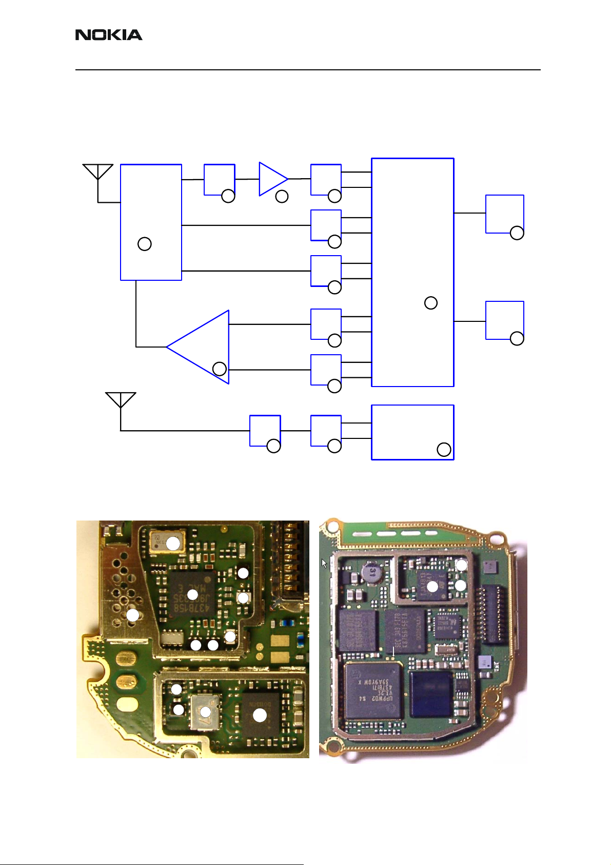
Receiver troubleshooting
General description
Figure 3: Receiver signal path
Page 10 © 2004 Nokia Corporation. Issue 3 09/2004
Page 11

Company Confidential RH-51/52, RH-67/68
Nokia Customer Care 6(b) - RF Troubleshooting
Each receiver path is a direct conversion linear receiver. From the antenna, the received
RF signal is fed to a front end module where a diplexer first divides the signal to two
separate paths according to the band of operation: either lower, GSM850/EGSM900 or
upper, GSM1800/1900 path. At each of the paths follows a pin-diode switch, which is
used to select either a receive- or transmit mode. At the upper band in the receive mode
either GSM1800 or 1900 path is further selected by another pin-diode switch. The selections are controlled by Helgo, which obtains the mode/band and timing information
through the RFBus. After the switches an external bandpass filter follows each receiver
paths. Thereafter, the signal is fed to the LNA's. GSM850/EGSM900 and GSM1800 LNA's
are integrated in Helgo, while the GSM1900 LNA is a discrete component placed
between SAW filter and balun. In GSM1900, the amplified signal is fed to a pre-gain
stage of the mixer. GSM850/EGSM900 and GSM1800 LNA's are connected directly to the
pregain stages. The pregain stages as well as all the following receiver blocks are integrated in Helgo. The LNA's have three gain levels. The first one is the maximum gain, the
second one is about 30 dB below the maximum, and the last one is the off state.
After the pregain stages there are demodulator mixers at each signal path to convert the
RF signal directly down to baseband I and Q signals. Local oscillator signals for the mixers are generated by an external VCO. The frequency is divided by two in GSM1800 and
GSM1900 and by four in GSM850/EGSM900. Those frequency dividers are integrated in
Helgo and in addition to the division they also provide accurate phase shifting by 90
degrees which is needed for the demodulator mixers.
The demodulator output signals are all differential. After the demodulators there are
amplifiers called DtoS (differential to single ended) which convert the differential signals
to single ended. Before that, they combine the signals from the three demodulators to a
single path which means that from the output of the demodulators to the baseband
interface are just two signal paths (I and Q), which are common to all the frequency
bands of operation. In addition, the DtoS amplifiers perform the first part of the channel
filtering and AGC (automatic gain control). They have two gain stages, the first one with
a constant gain of 12 dB and -3 dB bandwidth of 85 kHz and the second one with a
switchable gain of ±6 dB. The filters in the DtoS blocks are active RC filters. The rest of
the analog channel filtering is provided by blocks called BIQUAD which include modified
Sallen-Key biquad filters.
After the DtoS and BIQUAD blocks, there is another AGC-amplifier which provides a gain
control range of 42 dB in 6 dB steps. The correlation between the gain steps and the
absolute received power levels is found by a calibration routine in the production for
each assembled phone.
In addition to the AGC steps, the last AGC stage also performs the real time DC offset
compensation, which is needed in a direct conversion receiver to cancel out the effect of
the local oscillator leakage. DC offset compensation is performed during an operation
called DCN1. DCN1 is carried out by charging capacitors at the input of the last AGC
stages to a voltage, which causes a zero DC offset. To improve the accuracy a DC level
alignment possibility has been added to Helgo.
After the last AGC stages the single ended and filtered I- and Q-signals are fed to the RX
Issue 3 09/2004 © 2004 Nokia Corporation. Page 11
Page 12

RH-51/52, RH-67/68 Company Confidential
6(b) - RF Troubleshooting Nokia Customer Care
ADCs. The maximum peak-to-peak voltage swing for the ADCs is 1.45 V.
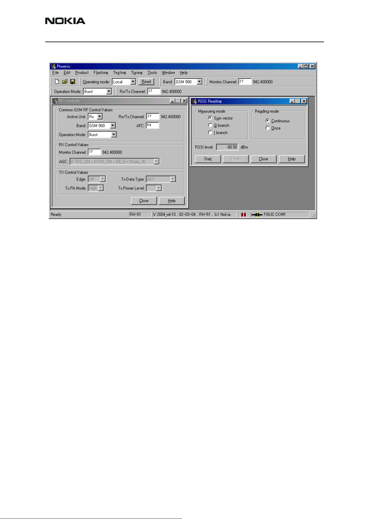
General instructions for RX troubleshooting
Connect the phone to a PC with DAU-9S cable and dongle and follow the following
instructions:
Measuring RX I/Q signals using RSSI
Start Phoenix Service Software and establish connection to the phone
Select File -> Open Product
RH-51, -52, -67 or -68
Select Testing ->RF controls
Select Band ->GSM850 / GSM900 / GSM1800 / GSM1900
Active unit ->RX
Operation mode ->Burst
RX/TX channel -> EGSM900: 37
GSM850: 190
GSM1800: 700
GSM1900: 661
Select
Testing (T)
RSSI Reading (R)
Set –up now looks like this:
Page 12 © 2004 Nokia Corporation. Issue 3 09/2004
Page 13
Company Confidential RH-51/52, RH-67/68
Nokia Customer Care 6(b) - RF Troubleshooting
Apply a signal with frequency of
EGSM900:942.4677MHz (channel 37 + 67.7KHz offset)
GSM850: 881.667MHz (channel 190 + 67.7KHz offset)
GSM1800:1842.8677MHz (channel 700 + 67.7KHz offset)
GSM1900:1960.0677MHz (channel 661 + 67.7KHz offset)
and a power level of –80dBm to the RF connector (remember to compensate for cable
loss).
In RSSI reading, click Read now.
The resulting RSSI level should be –80dBm in each band.
Issue 3 09/2004 © 2004 Nokia Corporation. Page 13
Page 14

RH-51/52, RH-67/68 Company Confidential
6(b) - RF Troubleshooting Nokia Customer Care
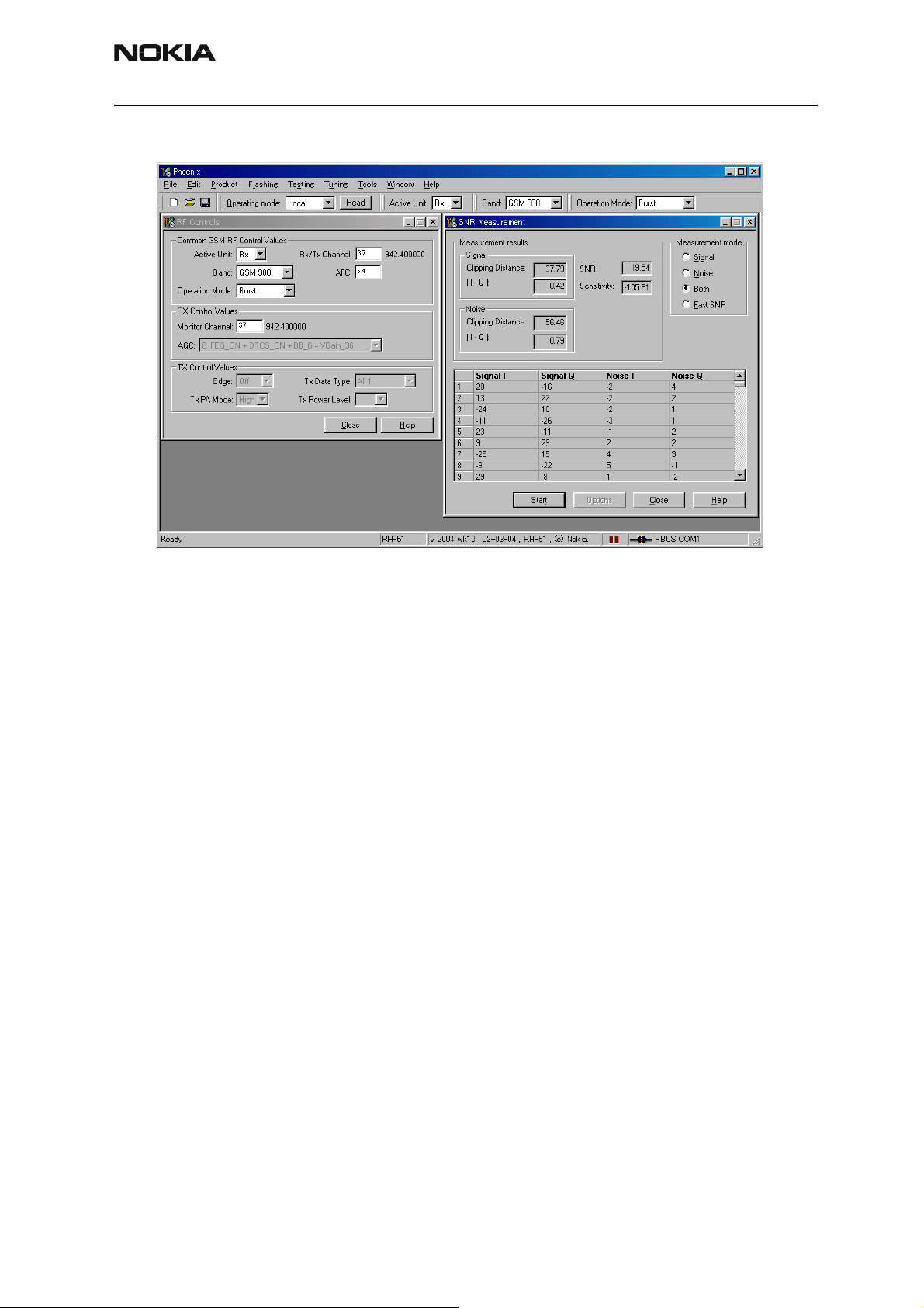
Measuring RX performance using SNR measurement
Note: This measurements also provides an indication of the conducted sensitivity
Start Phoenix Service Software and establish connection to the phone
Select File ->Open Product
RH-51, -52, -67 or -68
Select Testing ->RF controls
Select Band ->GSM850 / GSM900 / GSM1800 / GSM1900
Active unit ->RX
Operation mode ->Burst
RX/TX channel -> EGSM900: 37
GSM850: 190
GSM1800: 700
GSM1900: 661
Select Testing (T)
SNR Measurement (M)
select Both
Choose respective band (GSM850, EGSM900, GSM1800, GSM1900).
Press Start.
Follow the instructions for Signal generator set–up in the pop–up window.
Press OK.
Read the SNR result. SNR should be: >18dB.
Check the sensitivity value.
The set–up should now look like this; the icon also includes pop–up window for reference:
Page 14 © 2004 Nokia Corporation. Issue 3 09/2004
Page 15
Company Confidential RH-51/52, RH-67/68
Nokia Customer Care 6(b) - RF Troubleshooting
Measuring the RX module manually using oscilloscope and spectrum analyzer
Spectrum analyzer level values depend on the probe type and should be validated using a
known good sample. The levels that are given here are measured using a high frequency
probe.
Measuring with oscilloscope at test point RXI (J827) or RXQ (J828) ) and RXID (J261) or
RXQD (J262) is recommended only if RSSI reading does not provide enough information.
GSM 900/850
Start Phoenix Service Software and establish connection to the phone
Select File Open Product
RH-51, -52, -67 or -68
Select Testing RF controls
Select Band GSM900 (GSM850)
Active unit RX
Operation mode Continuous *
RX/TX channel 37 (190 for GSM850)
AGC 12
Issue 3 09/2004 © 2004 Nokia Corporation. Page 15
Page 16
RH-51/52, RH-67/68 Company Confidential
6(b) - RF Troubleshooting Nokia Customer Care
Input freq/level of signal generator is 942.4677MHz, -60dBm
(881.6677MHz for GSM850)
Note: Because DC compensation doesn’t work during continuous mode, DC offset level at RXI and RXQ will
gradually shift from the optimized level. To have most reliable result, it is highly advisable to set operation
mode from burst to continuous just before measuring values and complete measurement within no longer
than 30 seconds.
Figure 4: Troubleshooting chart for EGSM900 (GSM850)
EGSM900 (GSM850)
chain functional
Replace UPP
D370
942.4677 MHz (881.6677 MHz for GSM850)
YES
YES
Apply -60 dBm
from generator to antenna connector
Check RSSI using
Phoenix Does it
match Sig Gen
Output level ?
NO
Is L.O running at
3769.6MHz
(3526.4MHz for
GSM850?
YES
Probe J827, 828
RX I &Q Does waveform
look like example given
earlier ?
YES
Probe J261 &J263 Is
digital data visable ?
NO
Replace UEM
D250
NO
NO
Refer to Synthesiser
Fault -finding chart
Check RX/TX switch
at RX 900 Z800
Input -63 dBm
Output -63dbm
YES
Spectrum analyzer
EGSM SAW filter
Z803
output -66 dBm
YES
NO NO
NO
Oscilloscope
check Vc1, Vc2, Vc3
at Z800 signal 0V
YES
Check
RX/TX switch
Z800
Check SAW filter
Z803
Check HELGO
N500
Spectrum analyzer
Check signal after
inductors L804 and
L805
-66 dBm
YES
Oscilloscope
VR4 2.7 V
on N500
YES
NO
NO
Check inductors
L804, L805
Check UEM
D250
Page 16 © 2004 Nokia Corporation. Issue 3 09/2004
Page 17

Company Confidential RH-51/52, RH-67/68
Nokia Customer Care 6(b) - RF Troubleshooting
Figure 5: Probed RX I/Q signals J827, 828
Signal amplitude 180 ~ 600mVpp
DC offset 1.2 ~ 1.4V
Frequency approx 67KHz
GSM1800
Start Phoenix Service Software and establish connection to the phone.
Select File Open Product
Select Testing RF controls
Select Band GSM1800
Active unit RX
Operation mode Continuous *
RH-51, -52, -67 or 68
RX/TX channel 700
AGC 12
Issue 3 09/2004 © 2004 Nokia Corporation. Page 17
Page 18

RH-51/52, RH-67/68 Company Confidential
6(b) - RF Troubleshooting Nokia Customer Care
Input freq/level of signal generator is 1842.8677MHz, -60dBm
Note: Because DC compensation doesn’t work during continuous mode, DC offset level at RXI and RXQ will
gradually shift from the optimized level. To have most reliable result, it is highly advisable to set operation
mode from burst to continuous just before measuring values and complete measurement within no longer
than 30 seconds.
Figure 6: Troubleshooting chart for GSM1800
Apply -60 dBm
1842.8677 MHz
from generator to antenna
connector
Check RSSI using
YES
GSM1800 chain
functional
Phoenix Does it
match Sig Gen
Outp u t le v e l ?
NO
Replace UPP
D370
Is L.O running at
3685.6MHz?
YES
Probe J827,828
RX I &Q Does wave fo rm lo o k
like example given earlier ?
YES
YES
Probe J261 &J263
Is digital data
visable ?
NO
Replace UEM
D250
NO
Refer to Synthesiser
Fault -finding chart
Check RX/TX sw itch
NO
at RX 1800 Z800
Input -63 dBm
Output -65dBm
Spectrum analyzer GSM1800
SAW filter Z802
output -70 dBm
Spectrum analyzer
Check signal after inductors
L802 and L803
Oscilloscope
VRX 2.7 V on HELGO
YES
YES
-73 dBm
YES
N500
NO NO
NO
NO
NO
Oscilloscope
check Vc1, Vc2, Vc3
at Z800 signal 0V
YES
Check RX/TX switch
Z800
Check S A W filter
Check inductors
L802, L803
Check UEM
Z802
D250
Check HELGO
N500
YES
Page 18 © 2004 Nokia Corporation. Issue 3 09/2004
Page 19

Company Confidential RH-51/52, RH-67/68
Nokia Customer Care 6(b) - RF Troubleshooting
GSM1900
Start Phoenix Service Software and establish connection to the phone.
Select File Open Product
RH-51, -52, -67 or -68
Select Testing RF controls
Select Band GSM1900
Active unit RX
Operation mode Continuous *
RX/TX channel 661
AGC 12
Input freq/level of signal generator is 1960.0677MHz, -60dBm
Note: Because DC compensation doesn’t work during continuous mode, DC offset level at RXI and RXQ will
gradually shift from the optimized level. To have most reliable result, it is highly advisable to set operation
mode from burst to continuous just before measuring values and complete measurement within no longer
than 30 seconds.
Issue 3 09/2004 © 2004 Nokia Corporation. Page 19
Page 20

RH-51/52, RH-67/68 Company Confidential
6(b) - RF Troubleshooting Nokia Customer Care
Figure 7: Troubleshooting chart for GSM1900
Apply -60 dBm
1960.0677 MHz
from generator to antenna
connector
YES
GSM1900 chain
functional
Check RSSI using
Phoenix Does it
match Sig Gen
Output level ?
NO
Is L.O running at
3920.0MHz?
NO
Refer to Synthesiser
Fault -finding chart
Check RX/TX switch
Z800
Replace UPP
D370
Probe J827,828
RX I &Q Does waveform look
like example given earlier ?
YES
Probe J261 &J263 Is
digital data visable ?
Replace UEM
D250
YES
NO
YES
Check RX/TX switch
NO
at RX 1900 Z800
Input -63 dBm
Output -65 dBm
YES
Spectrum analyzer
GSM1900 SAW filter
Z801
output -70 dBm
YES
Spectrum analyzer
Check signal after
LNA V800
-55 dBm
YES
Spectrum analyzer
Check signal after
balun T800
-56 dBm
YES
Spectrum analyzer
Check signal after capacitor s
C805 and C806
-56 dBm
YES
YES
YES
NO NO
NO
NO
NO
NO
Oscilloscope
check Vc1, Vc2, Vc3
at Z800 signal Vc1,
Vc3 =0V
Vc2=2.7V
Check SAW filter
Z801
Check V800
Check balun
T800
Check
C805, C806 and
L807
Check HELGO
N500
Oscilloscope
VR4 2.7 V
on N500
YES
NO
Check UEM
D250
Page 20 © 2004 Nokia Corporation. Issue 3 09/2004
Page 21

Company Confidential RH-51/52, RH-67/68
p
p
p
p
Nokia Customer Care 6(b) - RF Troubleshooting
Measurement points in the receiver
Figure 8: Measurement points at RX frontend - part 1
L802, 803
output
L804, 805
GSM1900
ut
out
Z803
output
V800
output
Z800
output
Z801
ut
out
Z802
out
ut
Figure 9: Measurement points at RX frontend - part 2
C805, 806
out
ut
T800
output
Z800
VC2
Z800
VC1
Z800
GSM1800
output
Z800
EGSM900
(GSM850)
output
Z800
input
Z800
VC3
Issue 3 09/2004 © 2004 Nokia Corporation. Page 21
Page 22

RH-51/52, RH-67/68 Company Confidential
6(b) - RF Troubleshooting Nokia Customer Care
Figure 10: Measurement points at baseband IQ
J827
RXI
J828
RXQ
Figure 11: Measurement points at digital IQ
J261
RXID
J262
RXQD
Page 22 © 2004 Nokia Corporation. Issue 3 09/2004
Page 23

Company Confidential RH-51/52, RH-67/68
Nokia Customer Care 6(b) - RF Troubleshooting
Tuning RX using Phoenix
RX channel select filter calibration
This calibration calibrates the baseband filter inside Helgo ASIC. It is done by internally
measuring a prototype filter, for this reason the calibration is done once, not separately 3
bands.
This tuning doesn’t require RF input from an external signal generator.
Select Tuning RX Channel Select Filter Calibration
Check “Save to Phone”
Press Tune
Press Stop to store the data to the phone.
RX channel select filter calibration is finished.
RX calibration
The "RX calibration" is used to determine gain at different gain settings for front-end
and the Helgo ASIC and needs to be done in all three bands.
RX calibration requires an external signal generator.
Select Tuning RX calibration
Issue 3 09/2004 © 2004 Nokia Corporation. Page 23
Page 24

RH-51/52, RH-67/68 Company Confidential
6(b) - RF Troubleshooting Nokia Customer Care
Check Automatic calibration mode.
Check load from phone and Save to phone.
Press Start
Initial data will be loaded from the phone and calibration starts.
You will see following banner pops up.
Follow the instructions in the pop–up window and set frequency and level of the signal
generator
Press OK
Page 24 © 2004 Nokia Corporation. Issue 3 09/2004
Page 25

Company Confidential RH-51/52, RH-67/68
Nokia Customer Care 6(b) - RF Troubleshooting
Press “Save & Continue”
Calibration data will be stored to the phone and continue to the next band.
RX band filter response compensation
Rx band filter response compensation has 9 steps for each band.
Rx band filter response compensation requires an external signal generator.
Select Tuning RX Band Filter Response Compensation
Issue 3 09/2004 © 2004 Nokia Corporation. Page 25
Page 26

RH-51/52, RH-67/68 Company Confidential
6(b) - RF Troubleshooting Nokia Customer Care
Select Manual Tuning mode
Press Start.
Initial data will be loaded from the phone.
Press tune to start calibration.
Follow the instructions given in the following pop–up window and set frequency and
level of the signal generator.
Press OK to proceed to the next step.
After completely the 9 steps –calibration at 9 frequencies.
Test will be repeated for other bands.
Page 26 © 2004 Nokia Corporation. Issue 3 09/2004
Page 27

Company Confidential RH-51/52, RH-67/68
Nokia Customer Care 6(b) - RF Troubleshooting
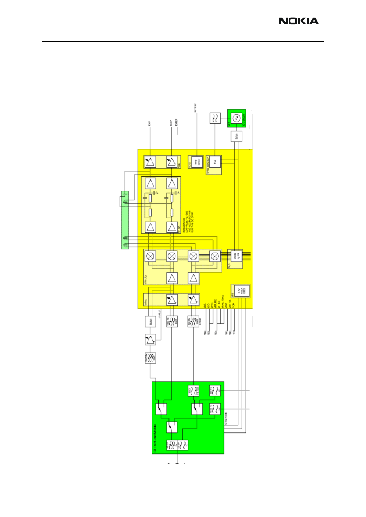
Transmitter troubleshooting
General description
A simple block diagram of the TX part of the phone is shown in the following figure. The
voice or data signals to be transmitted come from the UEME IC in the BB (baseband)
area, and go to the Helgo IC, where they are up-converted to RF. The TX signals going
from UEME to Helgo are called the IQ-signals, and consist of two balanced signals {
TXIN, TXIP } and { TXQN, TXQP }, i.e. a total of four signal lines. In addition to the IQ signals, there are also control signals going between BB and RF.
Figure 12: TX RF block diagram
BB-RF
Interface
Signals:
From UEME:
TXIQ
Helgo
4
V_BAT
1800 / 1900MHz
PA
Ant-Switch
1/2
900MHz
RFBusClk
RFBusEna1
RFBus Data
Reset
4
1/4
2
LO
Synthesizer
(LO=Local Oscillator)
VPCTRL_900
VPCTRL_1800_1900
SAW
2
Power Loop Filter
DET
The following picture shows the two shielding cans where the TX circuitry is located (the
lids have been removed). The upper shielding can contains BB-RF interface circuitry, the
Helgo RF system IC, a SAW filter for the GSM/EGSM band, and a balun for the DCS/PCS
band. The lower shielding can contains the power amplifier (PA) and the antenna switch
module (ASM).
Issue 3 09/2004 © 2004 Nokia Corporation. Page 27
Page 28

RH-51/52, RH-67/68 Company Confidential
6(b) - RF Troubleshooting Nokia Customer Care
(E)GSM
SAW filter
Helgo
DCS/PCS
Balun
Preparation for troubleshooting
• Place the phone (mechanics removed) on module jig.
• Connect the module jig to the PC via a DAU-9P cable.
• Connect the module jig to a power supply (4.2V).
• Connect the RF output to a spectrum analyzer or another measurement instrument.
Use a 10dB attenuator at the input to spectrum analyzer to avoid damaging it.
• Make sure the dongle is connected and start Phoenix.
• In Phoenix: File → Open Product → RH-51, -52, -67 or -68 Product Menu.
• Select Testing → RF Controls.
• From the toolbar: set Operating Mode to Local.
• Select band ‘GSM850’ ‘GSM900’, ‘GSM1800’ or ‘GSM1900’.
• Set Operation Mode to Burst.
ASM
hh
Power
Amplifier
• Set Active Unit to Tx.
• Set Tx Data Type to All 1.
• Set Rx/Tx Channel to 190 for GSM850, 37 for GSM900, 700 for GSM1800 or 661 for
GSM1900.
• Set Tx PA Mode to Free.
• Set Tx Power Level to 5 in GSM850/GSM900, otherwise to 0.
Page 28 © 2004 Nokia Corporation. Issue 3 09/2004
Page 29

Company Confidential RH-51/52, RH-67/68
Nokia Customer Care 6(b) - RF Troubleshooting
Phoenix should now look like this:
Issue 3 09/2004 © 2004 Nokia Corporation. Page 29
Page 30

RH-51/52, RH-67/68 Company Confidential
6(b) - RF Troubleshooting Nokia Customer Care
Fault-finding chart: TX-BB interface and control signals
Figure 13: Troubleshooting chart of TX-BB interface and control signals
TXC-signal
EGSM900
channel = 37
PL = 5
Figure 14: Oscilloscope screen shots
Typical oscilloscope plots
of the four TXIQ-line s:
6
zoom
1.1Vdc
TXP-signal
~67kHz
0.5Vpp
waveform for all 1's
4.615ms
VTXB_900
2.7V
Ctrl signals to ASM:
( DCS/PCS )
Cont1
Cont2
4.615ms
2.7V
4.615ms
4.
Page 30 © 2004 Nokia Corporation. Issue 3 09/2004
Page 31

Company Confidential RH-51/52, RH-67/68
Nokia Customer Care 6(b) - RF Troubleshooting
Fault-finding chart: RF side of transmitter
Figure 15: Troubleshooting chart of RF side of transmitter
Issue 3 09/2004 © 2004 Nokia Corporation. Page 31
Page 32

RH-51/52, RH-67/68 Company Confidential
6(b) - RF Troubleshooting Nokia Customer Care
ASM
Output
PA
850/900
Output
PA
1800/
1900
Output
PA
1800/
1900
Input
PA
850/
900
Input
VPCTRL 1800_1900
VBAT
VPCTRL 900
UPP
D370
J813
BT
D190
TXP
Page 32 © 2004 Nokia Corporation. Issue 3 09/2004
Page 33

Company Confidential RH-51/52, RH-67/68
Nokia Customer Care 6(b) - RF Troubleshooting
Issue 3 09/2004 © 2004 Nokia Corporation. Page 33
Page 34

RH-51/52, RH-67/68 Company Confidential
6(b) - RF Troubleshooting Nokia Customer Care
Transmitter tuning
In the transmitter there are two kinds of tunings that can be done; IQ tuning and power
level tuning. In general, different repairs require different tunings. In order to decide
which tuning is necessary after a repair, it is important to understand well the functionality of the repaired circuit. In general, it is recommended that if any TX component is
changed, both these tunings be done. All tunings are done in local mode, and using Phoe-
nix to control the phone.
In addition to that, note that the product has two different variants; RH-51, -67
(GSM900/GSM1800/GSM1900) and RH-52, -68 (GSM850/GSM1800/GSM1900), and
please proceed the tuning with corresponding bands for those variants. In this document,
some examples are described using GSM900 case, however please replace its description
as GSM850 if you handle the RH-52, -68 variant.
Also, as the RH-51/52, RH-67/68 doesn’t support EDGE feature, you don’t need to consider operating / tuning the phones in EDGE mode although Phoenix sometimes has a
control selectional box to enable EDGE.
TX IQ tuning
The tuning must be carried out in all three bands. In addition to Phoenix, a spectrum
analyzer (SA) is needed. Connect the SA to the RF connector of the module jig. The settings of the spectrum analyzer will depend on the band to be tuned. The following table
summarizes the settings for each of the three bands.
Table 1: Spectrum analyzer settings
GSM850 GSM900 GSM1800 GSM1900
Center frequency 836.6MHz 897.4MHz 1747.8MHz 1880MHz
Frequency span 300kHz 300kHz 300kHz 300kHz
Resolution Bandwidth 3kHz 3kHz 3kHz 3kHz
Video Bandwidth 3kHz 3kHz 3kHz 3kHz
Sweep Time 3 sec 3 sec 3 sec 3 sec
Trace Type Clear/Write Clear/Write Clear/Write Clear/Write
Detector Type Max Peak Max Peak Max Peak Max Peak
Reference Level 35dBm 35dBm 35dBm 35dBm
Marker 1 836.53229 MHz 897.33229 MHz 1747.73229 MHz 1879.93229 MHz
Marker 2 836.6 MHz 897.4MHz 1747.8MHz 1880MHz
Marker 3 836.66771 MHz 897.46771MHz 1747.86771MHz 1880.06771MHz
For this tuning, two windows of Phoenix must be open: (1) Testing → RF Controls, and
(2) Tuning → TX IQ Tuning, as seen in figures below.
Page 34 © 2004 Nokia Corporation. Issue 3 09/2004
Page 35

Company Confidential RH-51/52, RH-67/68
Nokia Customer Care 6(b) - RF Troubleshooting
Figure 16: Phoenix set-up (RF Controls menu)
Figure 17: Phoenix set-up (Tx IQ Tuning menu)
Issue 3 09/2004 © 2004 Nokia Corporation. Page 35
Page 36

RH-51/52, RH-67/68 Company Confidential
6(b) - RF Troubleshooting Nokia Customer Care
After opening the two before-mentioned windows, Phoenix should look like this:
Figure 18: Phoenix set-up (Tx IQ Tuning windows)
The following table summarizes the settings of the RF control window for IQ tuning of
the three bands.
Table 2: RF Control window settings
Band TX Data Type TX Power Level RX/TX Channel
GSM850 All 1 5 190
GSM900 All 1 5 37
GSM1800 All 1 0 700
GSM1900 All 1 0 661
To start the IQ tuning, press the ‘Start’ button in the IQ tuning window.
Page 36 © 2004 Nokia Corporation. Issue 3 09/2004
Page 37

Company Confidential RH-51/52, RH-67/68
A
5
5
Nokia Customer Care 6(b) - RF Troubleshooting
Figure 19: Spectrum analyzer screen shot when performing IQ tuning, part 1
Ref Lvl
Ref Lvl
35 dBm
35 dBm
3
27.5 dB Offset
30
20
10
Marker 1 [T1]
33.35 dBm
897.33229000 MHz
1
RBW 3 kHz
VBW 3 kHz
SWT 3 s
1 [T1] 33.35 dBm
897.33229000 MHz
2 [T1] -6.76 dBm
897.40000000 MHz
3 [T1] -10.74 dBm
897.46771000 MHz
RF Att 30 dB
Unit dBm
A
0
-10
-20
-30
-40
-50
-60
-6
Date: 14.JAN.2002 13:11:55
The purpose of this tuning is to reduce the frequency components at marker 2 (carrier
leakage) and marker 3 (+67kHz / upper sideband) as much as possible. Adjust the ‘TXI DC
Offset’ and the ‘TXQ DC Offset’ buttons in the TX IQ Tuning window so that the carrier
level (marker 2) reaches a minimum. After this adjustment is done, the carrier (marker 2)
should be at least 40dB below the lower side band (marker 1).
1M
2
3
30 kHz/Center 897.4 MHz Span 300 kHz
Next, use the ‘Amplitude difference’ and the ‘Phase difference’ buttons in the TX IQ Tuning window to adjust the upper side band (marker 3) to a minimum. Now, marker 3
should also be at least 40dB below marker 1.
At this point, the spectrum analyzer screen should look similar to that of the figure
below.
Issue 3 09/2004 © 2004 Nokia Corporation. Page 37
Page 38

RH-51/52, RH-67/68 Company Confidential
A
A
6(b) - RF Troubleshooting Nokia Customer Care
Figure 20: Spectrum analyzer screen shot when performing IQ tuning, part 2
Ref Lvl
Ref Lvl
35 dBm
35 dBm
Ref Lvl
Ref Lvl
35
35 dBm
35 dBm
27.5 dB Offset
30
35
27.5 dB Offset
30
20
20
10
10
0
0
10
-10
20
-20
30
-30
40
-40
50
-50
60
65
-60
-65
e: 14.JAN.2002 13:23:02
Date: 14.JAN.2002 13:23:02
33.40 dBm
Marker 1 [T1]
897.33229000 MHz
33.40 dBm
1
897.33229000 MHz
1
VBW 3 kHz
RBW 3 kHz
SWT 3 s
VBW 3 kHz
SWT 3 s
897.33229000 MHz
897.40000000 MHz
897.46771000 MHz
>40dB
>40dB
suppression
1 [T1] 33.40 dBm
2 [T1] -20.35 dBm
897.33229000 MHz
3 [T1] -27.60 dBm
897.40000000 MHz
897.46771000 MHz
RF Att 30 dB
Unit dBm
Unit dBm
1 [T1] 33.40 dBm
2 [T1] -20.35 dBm
3 [T1] -27.60 dBm
suppression
2
2
30 kHz/Center 897.4 MHz Span 300 kHz
30 kHz/Center 897.4 MHz Span 300 kHz
3
3
A
A
1M
1M
After reducing the amplitude of the frequency components at marker 2 and 3 to a minimum, press ‘Save & Continue’. The EGSM tuning has now been completed.
Now, using the spectrum analyzer settings listed in Table “Spectrum analyzer settings”
and the RF control settings listed in Table “RF Control window settings”, follow exactly
the same procedure to perform IQ tuning in the GSM1800 and GSM1900 bands.
Page 38 © 2004 Nokia Corporation. Issue 3 09/2004
Page 39

Company Confidential RH-51/52, RH-67/68
Nokia Customer Care 6(b) - RF Troubleshooting
TX power level tuning
This tuning is done separately in all three bands, and requires a spectrum analyzer to
measure the burst power of the GSM RF signal. When measuring the RF output (burst)
power on a spectrum analyzer, use the settings found in the following table:
Table 3: Spectrum analyzer settings for Tx power level tuning
GSM850 GSM900 GSM1800 GSM1900
Center frequency 836.6MHz 897.4MHz 1747.8MHz 1880MHz
Frequency span Zero-span Zero-span Zero-span Zero-span
Resolution Bandwidth 1MHz 1MHz 1MHz 1MHz
Video Bandwidth 1MHz 1MHz 1MHz 1MHz
Sweep Time 1ms 1ms 1ms 1ms
Trigger Type Video Video Video Video
Video trigger level Target pwr – 10dB Target pwr – 10dB Target pwr – 10dB Target pwr – 10dB
Trace Type Clear/Write Clear/Write Clear/Write Clear/Write
Detector Type Max Peak Max Peak Max Peak Max Peak
Reference Level Target power level +
10dB
Internal Attenuation Target power level +
10dB
Target power level +
10dB
Target power level +
10dB
Target power level +
10dB
Target power level +
10dB
Target power level +
10dB
Target power level +
10dB
In Phoenix, select Tuning → TX Power Level Tuning
Figure 21: Phoenix menu select (Tx Power Level Tuning menu)
Issue 3 09/2004 © 2004 Nokia Corporation. Page 39
Page 40

RH-51/52, RH-67/68 Company Confidential
6(b) - RF Troubleshooting Nokia Customer Care
Phoenix should now look similar to the figure below.
Figure 22: Phoenix Power Level Tuning menu
Connect the module jig RF output to the measurement instrument. The power must be
tuned in only high TX PA mode in all bands of GSM850, GSM900, GSM1800 and
GSM1900.
For each band, tune the power by adjusting the coefficient in the ‘Tx Power Level Tuning’
window in Phoenix until the target level is reached (measured on the spectrum analyzer).
Remember to take into account the external power loss, i.e. the loss of the cable and the
external attenuator at the spectrum analyzer input.
The coefficient must be tuned for the base level and other levels marked with bold letters
in Phoenix (GSM850/GSM900: PL19 / 15 / 5, GSM1800/1900: PL15, 11, 0). The target
power levels are specified as listed in the following table:
Table 4: Spectrum analyzer settings for Tx level tuning
GSM850 GSM900 GSM1800 GSM1900
LV5 32.5dBm LV5 32.5dBm LV0 30.0dBm LV0 30.0dBm
LV15 13.0dBm LV15 13.0dBm LV11 8.0dBm LV11 8.0dBm
LV19 5.0dBm LV19 5.0dBm LV15 0.0dBm LV15 0.0dBm
Base -27.0dBm Base -27.0dBm Base -27.0dBm Base -27.0dBm
When the tuning for the levels marked with bold letters has been completed, press ‘Cal-
Page 40 © 2004 Nokia Corporation. Issue 3 09/2004
Page 41

Company Confidential RH-51/52, RH-67/68
Nokia Customer Care 6(b) - RF Troubleshooting
culate coefficients’ to calculate the other power levels with non-bold letters.
When the coefficient calculation was done successfully, then press ‘Save & Continue’ to
save the new tuning values into the phone memory.
The following figure shows the power level tuning at the GSM900 band.
Figure 23: Phoenix screen shot (Tx Power Level Tuning)
The figure below shows one example from the spectrum analyzer screen during measuring the Tx power level.
Issue 3 09/2004 © 2004 Nokia Corporation. Page 41
Page 42

RH-51/52, RH-67/68 Company Confidential
6(b) - RF Troubleshooting Nokia Customer Care
Figure 24: Spectrum analyzer screen shot during power level tuning
Page 42 © 2004 Nokia Corporation. Issue 3 09/2004
Page 43

Company Confidential RH-51/52, RH-67/68
Nokia Customer Care 6(b) - RF Troubleshooting
Synthesizer troubleshooting
General description
Figure 25: Synthesizer block diagram
RFBusData
RFBusClk
AFC
8%1
NQQR
HKNVGT
/*\
RFBusEna1
Reset
RFCLK
LPRFCLK
1/2
PLL_BLOCK
1/4
EJCTIG
0&+8
RWOR
M
#&+8
4&+8
1/2
1/2
CNTROL
1/4
‡”
Issue 3 09/2004 © 2004 Nokia Corporation. Page 43
Page 44

RH-51/52, RH-67/68 Company Confidential
6(b) - RF Troubleshooting Nokia Customer Care
The PLL is capable of tuning frequency range for GSM band 850/900/1800/1900. Hence
PLL is common in all variants.
The VCO frequency is locked by a PLL (phase locked loop) into a stable frequency source
given by a VCTCXO, which is running at 26 MHz. The frequency of the VCTCXO is in turn
locked into the frequency of the base station with the help of an AFC (automatic frequency control) voltage, which is generated in UEME by an 11-bit D/A (digital-to-analog)
converter.
The PLL is integrated in Helgo and it is controlled through the RFBus. The PLL consists of
a 64/65 (P/P+1) prescaler, N- and A-divider, reference divider, phase detector and a
charge pump for the external loop filter. The 4 GHz oscillator signal, generated by the
VCO, is fed through a 180 degrees balanced phase shifter to the prescaler and the output
of the prescaler is fed to the N- and A-divider, which produces the input to the phase
detector. The phase detector compares this signal to the reference signal, which is
divided by the reference divider from the VCTCXO frequency. The frequency of the reference signal is 400 kHz. The output of the phase detector is connected to the charge
pump, which charges or discharges the integrator capacitor in the loop filter depending
on the phase of the measured frequency compared to the reference frequency. The integrator output voltage is finally connected to the control input of the VCO. The VCO operates at the channel frequency multiplied by two in DCS1800/PCS1900 and by four in
GSM850/EGSM900. The required frequency dividers for modulator and demodulator mixers are integrated in Helgo.
Loop filter filters out the comparison pulses of the phase detector and generates a DC
control voltage to the VCO. The loop filter determines the step response of the PLL (settling time) and contributes to the stability of the loop. Other filter components are for
sideband rejection. The dividers are controlled via the RFBus. RFBusData is for the data,
RFBusClk is a serial clock for the bus and RFBusEna1X is a latch enable, which stores the
new data into the dividers.
Page 44 © 2004 Nokia Corporation. Issue 3 09/2004
Page 45

Company Confidential RH-51/52, RH-67/68
Nokia Customer Care 6(b) - RF Troubleshooting
Figure 26: RF key component.
VCTXO 26MHz
G500
Balun 3-4GHz
T500
VCO 3-4GHz
G500
Assumption
Figure 27: Synthesizer key components without shielding frame
No failure i.e. soldering or component failure for simple SMD components such as resistors, inductors and capacitors.
Failure in one particular operating GSM channel whether Tx or Rx in which the synthesizer is the cause of the failure, all other GSM channel in Tx/Rx should fail.
Issue 3 09/2004 © 2004 Nokia Corporation. Page 45
Page 46

RH-51/52, RH-67/68 Company Confidential
6(b) - RF Troubleshooting Nokia Customer Care
Preparation for troubleshooting
• Place the phone (mechanics removed) on module jig.
• Connect the module jig to the PC via a DAU-9P cable.
• Connect the module jig to a power supply (4.2V).
• Connect the RF output to a spectrum analyzer or another measurement instrument.
• Use a 10dB attenuator at the input to spectrum analyzer to avoid damage.
• Make sure the dongle is connected and start Phoenix.
• In Phoenix: File → Open Product → RH-51, -52, -67 or -68 Product Menu.
• Select Testing → RF Controls.
• From the toolbar: set Operating Mode to Local.
• Select band “GSM 1800”.
• Set Operation Mode “Continuous”.
• Set Active Unit “Rx”.
• Set Rx/Tx Channel “700”.
Figure 28: Preparation for troubleshooting using Phoenix – RF control setup.
Page 46 © 2004 Nokia Corporation. Issue 3 09/2004
Page 47

Company Confidential RH-51/52, RH-67/68
Nokia Customer Care 6(b) - RF Troubleshooting
Measuring the synthesizer manually using spectrum analyzer
Spectrum analyzer level values depend on the probe type and should be validated using a
known good sample. The levels that are given here are measured using a high frequency
probe. Spectrum analyzer should be at least capable of measuring signal upto 4.5 GHz.
Troubelshooting chart for synthesizer
Figure 29: Troubleshooting chart for synthesizer
LOCAL OSCILLATOR
FAILURE
YES
Check
VCTXCO Output
min. 0.7p-p clipped sinewave
26MHz
OK
Check
VR1=Vcp=4.6-4.9V
VR5=Vpre=2.6-2.9V
OK
Check
VR7=VCO Vcc=2.6-2.9V
OK
Remove
HELGO/VCO
Shielding
Frame
NOK
NOK
NOK
Replace VCTXCO
G501
OK
Check
VCTCXO
Vcc=2.6-2.9V
Replace UEME
D250
Replace UEME
D250
NOK
NOK
Replace VCTXCO
G501
NOK
Replace UEME
D250
Replace HELGO
N500
Replace HELGO
N500
OK
VCO Output
Freq=3685.6Mhz
Power=-25 to-10dBm
Replace UEME
D250
Probe
NOK
Replace VCO
G500
NOK
Probe
VCO Output
Freq=3.0 to 4.5GHz
Power=-25 to-10dBm
OK
Probe Balun +/- output
Freq=3.0 to 4.5GHz
Power=-30 to-10dBm
OK
Replace HELGO
N500
NOKNOK
NOK
Replace VCO
G500
Replace
Attenuator&Balun
R503&T500
Issue 3 09/2004 © 2004 Nokia Corporation. Page 47
Page 48

RH-51/52, RH-67/68 Company Confidential
6(b) - RF Troubleshooting Nokia Customer Care
Figure 30: Measurement points for synthesizer. Layout shows HELGO/VCO compartment.
C526
VCTCXO Vcc
G501
VCTCXO Output
HELGO
N500
Balun +/- Output
T500
Figure 31: Measurement points for synthesizer. Layout shows UEME compartment
UEME
D250
G516
VR1=Vcp
C517
VR5=Vpre
G500
VCO RF Output
C301
VR7=VCO Vcc
Page 48 © 2004 Nokia Corporation. Issue 3 09/2004
Page 49

Company Confidential RH-51/52, RH-67/68
Nokia Customer Care 6(b) - RF Troubleshooting
Bluetooth troubleshooting
This document describes BC02 bluetooth solution troubleshooting for Care. Applicable
parts can be copied to phone products’ service document. It is assumed that the main
service manual includes part “How to connect Phoenix to phone”.
Bluetooth component placement
Figure 32: RH-51/52, RH-67/68 Bluetooth component placement
Bluetooth settings for Phoenix
Procedure:
1 Connect phone to Phoenix in ‘local’ mode.
2 Select product by: File −> Scan Product.
Issue 3 09/2004 © 2004 Nokia Corporation. Page 49
Page 50

RH-51/52, RH-67/68 Company Confidential
6(b) - RF Troubleshooting Nokia Customer Care
3 Choose: Testing −> Bluetooth LOCALS
4 Locate JBT-9’s Ser.No. (12 digits from the type label) found in the type label in
the back of JBT-9.
5 In the Bluetooth LOCALS setting enter Ser.No. for the “Counterpart Device
Address” field. This has to be done only once provided JBT-9 is not changed.
6 Run BER test when JBT-9 box is proximity of the DUT’s Bluetooth antenna. Suit-
able distance is approximately 10 centimeter.
Page 50 © 2004 Nokia Corporation. Issue 3 09/2004
Page 51

Company Confidential RH-51/52, RH-67/68
Nokia Customer Care 6(b) - RF Troubleshooting
Figure 33: Phoenix settings for Bluetooth troubleshooting
Issue 3 09/2004 © 2004 Nokia Corporation. Page 51
Page 52

RH-51/52, RH-67/68 Company Confidential
6(b) - RF Troubleshooting Nokia Customer Care
Bluetooth troubleshooting diagram
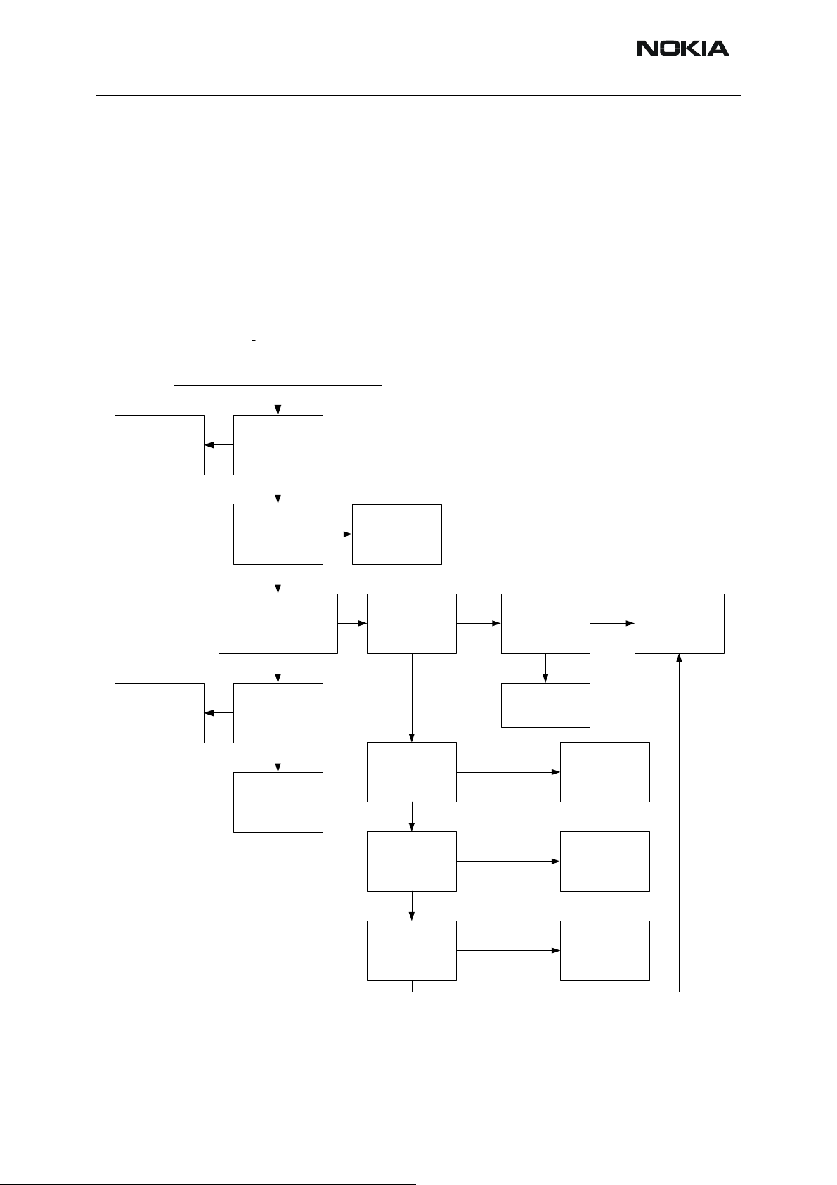
Figure 34: Bluetooth troubleshooting flowchart
Bluetooth fault
Replace BC02
(D190)
Connection to
JBT9 OK ?
N
Is BC02 VREG_IN =
2.8V at C203?
Is BC02 VDD_ANA
= 1.8V at C201
N
Y
Y
BER <=
0.1%?
Y
Bluetooth ok
N
N
Vflash1 from
UEME not
supplied
1)
Check component
soldering in RF path
(Z191, Z192, C191,
C192, L191, L192)
2)
Replace balun
and filter
(Z191, Z192)
3)
Replace BC02
(D190)
Y
Replace
inverter (D191)
Reference clock
from HELCO not
supplied
1)
N
2)
Is BC02 Xtal_in
(1) frequency = 26MHz
(2) voltage swing = about
1000mV
Y
Page 52 © 2004 Nokia Corporation. Issue 3 09/2004
 Loading...