

Page 1

Nokia Customer Care
RH-51/52, RH-67/68 Series Cellular Phones
7 - System Module
Issue 3 09/2004 © 2004 Nokia Corporation. Page 1
Company Confidential
Page 2

RH-51/52, RH-67/68 Company Confidential
7 - System Module Nokia Customer Care
This page has been deliberately left blank
Page 2 © 2004 Nokia Corporation. Issue 3 09/2004
Page 3

Company Confidential RH-51/52, RH-67/68
Nokia Customer Care 7 - System Module
Table of Contents
Page No
Glossary of terms......................................................................................................................................5
Introduction ...............................................................................................................................................6
System module block diagram ..........................................................................................................6
Functional description.............................................................................................................................7
BB description .......................................................................................................................................7
Memory configuration ......................................................................................................................7
Energy management.......................................................................................................................... 8
Modes of operation ..............................................................................................................................8
Voltage limits.......................................................................................................................................9
Clocking scheme ...................................................................................................................................9
UPP_WD2 voltage/clock frequency adjusting.........................................................................10
Power distribution, control and reset ...........................................................................................10
Power-up sequence (reset mode).................................................................................................11
Powering off.......................................................................................................................................11
Controlled powering off..................................................................................................................11
Uncontrolled powering off.............................................................................................................11
Watchdogs..........................................................................................................................................11
Charging..............................................................................................................................................12
Chargers...............................................................................................................................................12
Battery .................................................................................................................................................12
Back-up battery and real time clock ............................................................................................12
Baseband measurement A/D converter ........................................................................................12
ZOCUS........................................................................................................................................................13
RH-51/52, RH-67/68 baseband features and HW interfaces....................................................14
RH-51/52, RH-67/68 BB user interface .......................................................................................14
UI-module interface.........................................................................................................................14
Bluetooth ..............................................................................................................................................14
USB .........................................................................................................................................................14
SIM interface .......................................................................................................................................14
MMC interface ....................................................................................................................................14
RF PopPortTM ..................................................................................................................
RH-51/52, RH-67/68 audio concept .............................................................................................15
Earpiece ...............................................................................................................................................15
Microphone ........................................................................................................................................16
IHF amplifier and speaker...............................................................................................................16
External audio interface .................................................................................................................16
Camera interface ................................................................................................................................17
Flashing .................................................................................................................................................17
Testing interfaces ...............................................................................................................................18
Extreme voltages ...............................................................................................................................19
Temperature conditions ....................................................................................................................19
Humidity and water resistance ......................................................................................................19
RF description..........................................................................................................................................20
....................14
Issue 3 09/2004 © 2004 Nokia Corporation. Page 3
Page 4

RH-51/52, RH-67/68 Company Confidential
7 - System Module Nokia Customer Care
List of Figures
Page No
Fig 1 Module block diagram ...................................................................................................................6
Fig 2 RH-51/52, RH-67/68 clocking.................................................................................................. 10
Fig 3 RH-51/52, RH-67/68 audio blocks.......................................................................................... 15
Fig 4 External audio connector........................................................................................................... 17
Page 4 © 2004 Nokia Corporation. Issue 3 09/2004
Page 5

Company Confidential RH-51/52, RH-67/68
Nokia Customer Care 7 - System Module
Glossary of terms
ASIC Application Specific Integrated Circuit
BB Baseband
BT Bluetooth
BSI Battery Size Indicator
CBus MCU controlled serial bus connected to UPP_WD2,UEME and Zocus
CCP Compact Camera Port
CPU Central Processing Unit
DBus DSP controlled serial bus connected between UPP_WD2 and Helgo
DSP Digital Signal Processor
EGSM Extended – GSM
GPRS General Packet Radio Service
GSM Group Special Mobile/Global System for Mobile communication
HF Hands free
HFCM Handsfree Common
HS Handset
I/O Input/Output
IHF Integrated hands free
JPEG Joint Photographic Experts Group
LCD Liquid Crystal Display
MCU Micro Controller Unit
MIC, mic Microphone
PDA Pocket Data Application
PWB Printed Wiring Board
RF Radio Frequency
RFBUS Serial control Bus For RF
RF PopPort
TM
Reduced function PopPortTM interface
RS-MMC Reduced size Multi Media Card
SDRAM Synchronous Dynamic Random Access Memory
SIM Subscriber Identity Module
UI User Interface
UEME Universal Energy Management chip (Enhanced version)
VCXO Voltage Controlled Crystal Oscillator
Issue 3 09/2004 © 2004 Nokia Corporation. Page 5
Page 6
RH-51/52, RH-67/68 Company Confidential
7 - System Module Nokia Customer Care
Introduction
The system module RH-51/52, RH-67/68 consists of radio frequency (RF) and baseband
(BB), including user interface (UI) with keyboard.
System module block diagram
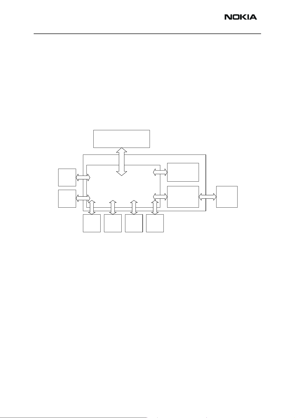
The 1BZ system module is the engine board of the RH-51/52, RH-67/68 phone. It
includes the baseband and RF functions of the phone and Bluetooth and camera modules
as shown in the figure below. External interfaces are drawn as arrows crossing the 1BZ
border.
Figure 1: Module block diagram
Flashing and Testing
Interface
1BZ module
RF
Pop-port
Baseband
Bluetooth
MMC
Card
MegaPixel
Camera
Module
RF
AudioUI
SIM
Card
GSM
antenna
The accessory interface is provided by Bluetooth and Reduced Function PopPortTM. RH51/52, RH-67/68 has a PopPortTM connector but no ACI interface internally, so it’s called
the RF PopPortTM.
RH-51/52, RH-67/68 uses the same connector as another PopPortTM phone but it can’t
communicate with ACI accessory. Monoural headsets, charger and camera flash are
interfaced via the RF PopPortTM and BT headset, and some BT accessories are interfaced
via Bluetooth.
Page 6 © 2004 Nokia Corporation. Issue 3 09/2004
Page 7

Company Confidential RH-51/52, RH-67/68
Nokia Customer Care 7 - System Module
Functional description
The heart of the BB is UPP_WD2, which includes the MCU, DSP and Digital Control Logic.
Power is supplied by the UEME ASIC and a number of discrete regulators. Memory comprises of 2 x 128Mbit Stacked and 64Mbit flash memory devices and 128 Mbit (16
Mbytes) SDRAM.
There are two audio transducers (earpiece 8 mm and IHF speaker 16 mm) and external
galvanic headset (PopPort
tone. The IHF speaker is driven by a discrete audio amplifier. In RH-51/52, RH-67/68
there is only one microphone for both HS and IHF modes.
For data connectivity there is USB v2.0 full-speed, Bluetooth and RS-MMC card.
The display is an TFT type colour display with 65536 colours and 176x208 pixels with
backlighting. The UI module features a round keymat and a navigation key.
For imaging purposes, BB supports a mega-pixel camera via the CCP interface, which is
integrated in UPP_WD2.
TM
) interface. The IHF speaker is also used to handle the ring
BB description
The BB core is based on UPP_WD2 CPU, which is a PDA version of the DCT4 UPP ASIC.
UPP_WD2 takes care of all the signal processing and operation controlling tasks of the
phone as well as all PDA tasks.
For power management, there is one main ASIC for controlling charging and supplying
power UEME plus some discrete power supplies. The main reset for the system is generated by the UEME.
The interface to the RF and audio sections is also handled by the UEME. This ASIC provides A/D and D/A conversion of the in-phase and quadrature receive and transmit signal
paths and also A/D and D/A conversions of received and transmitted audio signals. Data
transmission between UEME and RF and the UPP_WD2 is implemented using different
serial connections (CBUS, DBUS and RFBUS). Digital speech processing is handled by
UPP_WD2 ASIC.
A real time clock function is integrated into UEME, which utilizes the same 32kHz-clock
source as the sleep clock. A rechargeable battery provides backup power to run the RTC
when the main battery is removed. Backup time is approximately 5 Hours.
Memory configuration
RH-51/52, RH-67/68 uses two kinds of memories, Flash and SDRAM. These memories
have their own dedicated bus interfaces to UPP_WD2.
Synchronous DRAM is used as the working memory. Interface is 16 bit wide data and 14
bit address. Memory clocking speed is 123.5 MHz. The SDRAM size is 128Mbits.
SDRAM I/O is 1.8 V and core 1.8 V supplied by UEME regulator VIO. All memory contents
Issue 3 09/2004 © 2004 Nokia Corporation. Page 7
Page 8

RH-51/52, RH-67/68 Company Confidential
7 - System Module Nokia Customer Care
are lost if the supply voltage is switched off.
Multiplexed flash memory interface is used to store the MCU program code and user
data. The memory interface is a burst type FLASH with multiplexed address/data bus,
running at 123.5/3MHz.
Configuration of flash memory is a 2x128Mbit stacked flash memory and a 64Mbit flash
memory.
Both flash I/O and core voltage are 1.8 V supplied by UEME’s VIO.
Energy management
The master of EM control is UEME and with SW it has the main control of the system
voltages and operating modes.
Modes of operation
RH-51/52, RH-67/68 employs several hardware and software controlled operation
modes. Main modes are described below.
• NO_SUPPLY mode means that the main battery is not present or its voltage is too
low (below UEME master reset threshold) and back-up battery voltage is too low.
• In BACK_UP mode the main battery is not present or its voltage is too low but the
back-up battery has sufficient charge in it.
• In PWR_OFF mode the main battery is present and its voltage is over the UEME master reset threshold. All regulators are disabled.
• RESET mode is a synonym for start-up sequence and contains in fact several modes.
In this mode, regulators and oscillators are enabled and after they have stabilized
system reset is released and PWR_ON mode entered.
• In PWR_ON mode SW is running and controlling the system.
• SLEEP mode is entered from PWR_ON mode when the system’s activity is low
(SLEEPX controlled by SW).
• FLASHING mode is for production SW download.
Page 8 © 2004 Nokia Corporation. Issue 3 09/2004
Page 9

Company Confidential RH-51/52, RH-67/68
Nokia Customer Care 7 - System Module
Voltage limits
The voltage limits of the system are listed in the following table. These are also controlling system states.
Parameter Description Value
V
MSTR+
V
MSTR-
V
COFF+
V
COFF-
V_BU
V_BU
SW
COFF
COFF+
COFF-
Master reset threshold (rising) 2.1 V (typ.)
Master reset threshold (falling) 1.9 V (typ.)
Hardware cutoff (rising) 3.1 V (typ.)
Hardware cutoff (falling) 2.8 V (typ.)
Back-up battery cutoff (rising) 2.1 V (typ.)
Back-up battery cutoff (falling) 2.0 V (typ.)
SW cutoff limit (> regulator drop-out limit) MIN! 3.4 V SW changeable
The master reset threshold controls the internal reset of UEME. If battery voltage is
above V
MSTR
the main battery. Above V
may not succeed due to voltage drops during start-up. SW can also consider battery
voltage too low for operation and power down the system.
Clocking scheme
A 26 MHz VCXO is used as system clock generator in GSM. During the system start-up,
UEME RC-oscillators generate timing for state machines. All clock signals of the engine
are illustrated in following figure.
, UEME’s charging control logic is alive. Also, RTC is active and supplied from
UEME allows the system to be powered on although this
MSTR
Bluetooth uses a 26 MHz clock.
In SLEEP mode, the VCXO is off. UEME generates low frequency clock signal (32.768 kHz)
that is fed to UPP_WD2, Bluetooth and ZOCUS.
Issue 3 09/2004 © 2004 Nokia Corporation. Page 9
Page 10

RH-51/52, RH-67/68 Company Confidential
7 - System Module Nokia Customer Care
Figure 2: RH-51/52, RH-67/68 clocking.
UPP_WD2 voltage/clock frequency adjusting
No external clock is available for UPP_WD2 before VCXO starts. As reset is released, the
VCXO is running and MCU uses the 26 MHz clock while DSP is in reset. There are three
identical DPLL's, for MCU, for DSP and for accessory interfaces, which can be controlled
independently. The clock for MCU can be up to 130 MHz and 156 MHz is maximum clock
frequency for the DSP. These clock signals are used either directly (SDRAM IF) or divided
down for the interfaces (e.g. flash IF).
Power distribution, control and reset
All power (except backup battery power) is drawn from the BL-5C Li-Ion battery located
in the B cover. Current flows through ZOCUS current sense resister which is used for current measurement by ZOCUS and thus for remaining operating time estimation.
1BZ board contains one power ASIC, UEME and discrete regulators needed for generating
Page 10 © 2004 Nokia Corporation. Issue 3 09/2004
Page 11

Company Confidential RH-51/52, RH-67/68
Nokia Customer Care 7 - System Module
the different operating voltages. The discrete regulators consist of an SMPS to power
UPPWD2 voltage core. In addition, there is a SMPS in 1BZ generating the operating voltage for display module backlighting. In 1BZ, the keyboard backlight is powered with a
charge pump regulator.
Power-up sequence (reset mode)
RESET mode can be entered in four ways: by inserting the battery or charger, by RTC
alarm or by pressing the power key. The VCXO is powered by UEME. After a 220 ms delay,
regulators are configured and UEME enters PWR_ON mode and system reset PURX is
released.
During the system start-up, in RESET state, the regulators are enabled, and each regulator charges the capacitor(s) at the output with the maximum current (short circuit current) it can deliver. This results in battery voltage dropping during start-up. When a
battery with a voltage level just above the hardware cutoff limit is inserted, the system
may not start due to excessive voltage dipping. Dropping below 2.8 V for longer than 5
us forces the system to PWR_OFF state.
Powering off
Controlled powering off is done when the user requests it by pressing the power-key or
when the battery voltage falls too low. Uncontrolled powering off happens when the
battery is suddenly removed or if over-temperature condition is detected in regulator
block while in RESET mode. Then all UEME’s regulators are disabled immediately and discrete regulators are disabled as Vbat supply disappears.
Controlled powering off
For RH-51/52, RH-67/68, powering off is initiated by pressing the power key and power
off sequence is activated in UEME and SW. Basically, the power key causes UEME interrupt to UPP_WD2 and SW sets watchdog time value to zero and as this happens, PURX is
forced low and all regulators are disabled.
If the battery voltage falls below the very last SW-cutoff level, SW will power off the
system by letting the UEME’s watchdog elapse.
If thermal shutdown limit in the UEME regulator block is exceeded, the system is powered off. System reset PURX is forced low.
Uncontrolled powering off
This happens when the battery is suddenly removed. UEME’s state machine notices battery removal after the battery voltage has been below V
PWR_OFF mode. PURX is set low and all UEME’s regulators are disabled.
for 5 us and enters
COFF-
Watchdogs
There are three watchdogs in UEME. The first one is for controlling system power-on and
power-down sequences. The initial time for this watchdog after reset is 32 s and the
watchdog can not be disabled. The time can be set using a register. This watchdog is used
for powering the system off in a controlled manner. The other one is for security block
Issue 3 09/2004 © 2004 Nokia Corporation. Page 11
Page 12

RH-51/52, RH-67/68 Company Confidential
7 - System Module Nokia Customer Care
and is used during IMEI code setting. The third one is a power key watchdog. It is used to
power off the system in case SW is stuck and the user presses the power key. This WD is
SW configurable.
There is also a “soft watchdog” in UPP_WD2. It is used to reset the chip in case software
gets stuck for any reason.
Charging
Charging control and charge switch is in UEME. There are two different charging modes;
charging an empty battery (start-up charge mode), and SW controlled charging.
UEME digital part takes care of charger detection (generates interrupt to UPP_WD2),
pulse width modulated charging control (for internal charge switch) and over voltage
and current detection. SW using registers controls all these.
Chargers
RH-51/52, RH-67/68 BB supports a standard charger (two wires); ACP-12 and cigarette
charger LCH-12 officially.
Battery
RH-51/52, RH-67/68 battery is a detachable, semi-fixed lithium-Ion BL-5C battery. The
nominal voltage is thus 3.7 V (max charging voltage 4.2 V).
The interface consists of three pins: VBAT, GND and BSI. A pull-down resistor inside the
batteries (BSI signal) recognizes the battery types. The voltage level at BSI line is measured using UEME's AD-converter.
Back-up battery and real time clock
The real time clock (RTC), crystal oscillator and back-up battery circuitry reside in UEME.
A register in UEME controls back-up battery charging and charging is possible only in
POWER_ON State.
Baseband measurement A/D converter
UEME contains an 11 channels A/D converter, which is used for different baseband
measurement purposes. The resolution of the A/D converter is 10 bits. The converter uses
the CBUS interface clock signal for the conversion. An interrupt will be given to the MCU
at the end of the measurements. The converter is used for following purposes.
• Battery Voltage Measurement A/D Channel (Internal)
• Charger Voltage Measurement A/D Channel (Internal)
• Charger Current Measurement A/D Channel (Internal)
• Battery Temperature Measurement A/D Channel (External)
• Battery Size Measurement A/D Channel (External)
• LED Temperature measurement A/D Channel (External)
There is also an auxiliary AD converter in UEME, which is used to monitor RF functions.
Page 12 © 2004 Nokia Corporation. Issue 3 09/2004
Page 13

Company Confidential RH-51/52, RH-67/68
Nokia Customer Care 7 - System Module
ZOCUS
The ZOCUS device is a current sensor used for the battery bar display and for determining
whether the phone is in a high current consuming mode. The ZOCUS device measures the
voltage drop across a sense resistor in the battery voltage line. This sense resistor is
formed from a PWB track and is on an internal layer of the PWB. The sense resistor must
be located close to the battery terminals so that all of the phones current flow through
it. The nominal value of the sense resistor is 3.0m-ohm. ZOCUS reports the current measurement to UPP_WD2 via the Cbus interface.
Issue 3 09/2004 © 2004 Nokia Corporation. Page 13
Page 14

RH-51/52, RH-67/68 Company Confidential
7 - System Module Nokia Customer Care
RH-51/52, RH-67/68 baseband features and HW interfaces
RH-51/52, RH-67/68 BB user interface
UI-module interface
The UI-module consists of the LCD and keymat. The colour display resolution is 176 x 208
and backlighting is via 4 white LED’s. The display is connected to the 1BZ module via an
24 pin plug and socket. The keymat is connected to 1BZ by 20-pin contact type connector. The interface also includes power rails for keypad backlight. The keymat interface
uses GPIO pins of UPP_WD2.
Bluetooth
Bluetooth provides a fully digital link for communication between a master unit and one
or more slave units. The system provides a radio link that offers a high degree of flexibility to support various applications and product scenarios. Data and control interface for
a low power RF module is provided. Data rate is regulated between the master and the
slave.
USB
USB provides a wired connectivity between host PC and peripheral devices. RH-51/52,
RH-67/68 complies with USB 2.0, supporting data transfer at full-speed (max. 12Mbps).
The USB functionality of RH-51/52, RH-67/68 is implemented by a newly developed USB
interface device, Kaede (NMP code is 4342163), which is connected to UPP_WD2 via
flash memory interfaces. A 6MHz ceramic resonator, Ceralock (NMP code is 451B099), is
used for USB clock generation.
SIM interface
The SIM interface is located in two chips (UPP_WD2 and UEME). In UEME there is support only for one SIM card. The interfaces support both 1.8 V and 3 V SIM cards. Adjustable SIM regulator (1.8V/3.0V) is located in UEME and can be controlled by SW.
The data communication between the card and the phone is asynchronous half duplex.
The clock supplied to the card is 3.25 MHz. The data baudrate is SIM card clock frequency divided by 372 (by default), 64, 32 or 16.
MMC interface
The MMC interface consists of a block in UPP_WD2 plus a level shifting device known as
“Lester” and an EMC protection ASIP. The MMC interface comprises 3 lines clock, data
and command and runs at 8.66 MHz. The Lester device also incorporates a 2.85V regulator to power the MMC card.
RF PopPortTM
RH-51/52, RH-67/68 use same PopPortTM connector same as other PopPortTM phones but
it can’t communicate with ACI accessory such as HDS-3 stereo headset due to the lack of
ACI module in UPP_WD2.
Page 14 © 2004 Nokia Corporation. Issue 3 09/2004
Page 15

Company Confidential RH-51/52, RH-67/68
Nokia Customer Care 7 - System Module
Multiplexed data lines of USB and Fast-Fbus are also single usage for USB only cause
USB chip doesn’t have such functionality.
Hence there’s no PopPort
TM
stereo headset without ACI chip in it, RH-51/52, RH-67/68
uses only the mono headset interface.
RH-51/52, RH-67/68 audio concept
RH-51/52, RH-67/68 audio includes an earpiece, a microphone, and a PopPortTM connector for headset and integrated handsfree (IHF). Audio is based on ASIC's UPP_WD2,
UEME and a discrete amplifier for the handsfree speaker known as “boomer”.
Figure 3: RH-51/52, RH-67/68 audio blocks
UPP WD2
EAR DATA
MIC DATA
UEME
EarP
EarN
MicB1
Mic1P
Mic1N
PAoutP
PAoutN
EAR
MIC
LM4890
IHF
Earpiece
HF
HFCM
Camera flash
Hookint
MicB2
Mic2P
Mic2N
Headint Pin- 3: ACI
acc essory
detect circuit
Pin- 12: HS EARP
Pin- 11: HSEARN
Pin- 10: XMIC P
Pin- 9: XMICN
Pop- port
connector
Between UPP_WD2 and UEME, the audio signals are transferred in digital format using
signals MICDATA and EARDATA. Ringing tones and warning/info tones are to be produced to the IHF speaker.
The earpiece to be used in RH-51/52, RH-67/68 is an 8-mm Pico earpiece produced by
Philips Speaker Systems. It has 32
Ω continuous impedance and continuous power 8
Issue 3 09/2004 © 2004 Nokia Corporation. Page 15
Page 16

RH-51/52, RH-67/68 Company Confidential
7 - System Module Nokia Customer Care
mWatts. It's driven by differential signals from UEME (EARP & EARN). It makes contact
with the PWB via spring contacts.
Microphone
The microphone module for RH-51/52, RH-67/68 is used PopPortTM microphone module.
Its sensitivity is -42dB Nominal. Contacts are done by springs.
Two inputs are used from UEME, one for the normal internal microphone and the other
for the headset. The third microphone input is not used, so it is connected to ground via
capacitors. Microphone bias block in UEME generates bias voltages for handportable and
handsfree/headset microphones. For both microphone bias outputs (MICB1 & MICB2),
the minimum output voltage is 2.0 Volts and maximum output current is 600
µA. Micro-
phone bias block also includes a low pass filter for the reference voltage used as an input
for the MICB1&2 amplifiers.
IHF amplifier and speaker
The speaker to be used in RH-51/52, RH-67/68 is a 16mm 8Ω speaker. It can handle 0.3
Watts nominal power and short trem peak power of 0.8 Watts. The component is housed
in the antenna housing and connects to the PWB via spring contacts.
PAOUTP and PAOUTN lines of UEME are use to drive Boomer IHF amplifier.
Power amplifier is a differential opamp. The differential output drives the HandsFree
speaker. HandsFree amplifier load impedance is 8 ohm.
The outputs go into a high impedance state when powered down. The amplifier can be
enabled and shut down using a GENIO line from UPP_WD2.
SW controls IHF, headset and earpiece volume via UEME. Gain setting can be done in 2
dB steps, from –40 to +6 dB. The output sound pressure level of the internal HandsFree
speaker is controlled by SW (CBus is used for controlling).
The schematic around the Boomer IHF amplifier is presented in RH-51/52, RH-67/68
schematics. The schematic shows all the filtering needed and also protection components against ESD and EMC. The EMC and ESD filtering component must be as near as
possible to the earphone pads of the phone.
The supply voltage for the IHF amplifier is taken directly from the battery voltage.
External audio interface
In RH-51/52, RH-67/68 there is a PopPortTM connector which is fully differential 4–wire
connection.
Page 16 © 2004 Nokia Corporation. Issue 3 09/2004
Page 17

Company Confidential RH-51/52, RH-67/68
Nokia Customer Care 7 - System Module
Figure 4: External audio connector
PWB
The handsfree (HF) driver in UEME is meant for the headset. In RH-51/52, RH-67/68, the
output is driven in fully differential mode. In the fully differential mode, the HF pin is the
negative output and the HFCM pin is the positive output. The gain of the handsfree
driver in the differential mode is 6 dB. The earpiece (EARP, EARN) and headset (HF,
HFCM) signals are multiplexed so that the outputs can not be used simultaneously. The
HF and HFCM amplifiers include a transient suppression circuitry, which prevents
unwanted spikes in HF and HFCM outputs when switching on and off the amplifiers.
The HeadInt line will be pulled up to 2.7V by the internal resistor when the accessory is
connected. When not having the accessory inserted the voltage in the HeadInt line will
be <0.8 V caused by internal pull down resistor in the HF line.
Camera interface
RH-51/52, RH-67/68 has a digital still camera with viewfinder function. The camera resolution is VGA (640 x 480 pixels) and 1M Pixel (1152 x 864 pixels). The camera module is
connected by means of a soldered on connector to the PWB.
The camera interface is a serial CCP, which is an unidirectional interface; the control
information to camera is transmitted through I2C bus. The I2C bus is implemented purely
by the SW using general purpose I/Os.
GND
ChargeGND
VChar
Shielding
Headint (ACI)
Vout
USB D-
USB D+
USB Vbus
XMIC N
DATA GND
XMIC P
HEAR N
P
HEAR
XHEARNR
GND
XHEARPR
Shielding
The CCP interface consists of differential clock and data signals. The CCP enables the use
of high data rates with low EMI; maximum transfer capacity is 108Mbit/s, which means
that transferring YUV VGA(640 x 480) or 1Mp JPEG encoded images at 15fps is possible.
The camera needs two power sources, 2.5V for analog circuit voltage VDD and 1.5V for
digital circuit voltage VDDI. VDD is provided from same discrete regulator as LCD and
VDDI is fed from UEME’s Vcore.
Flashing
SW download in service is implemented by custom tools and SW, kindly refer to Service
Software Instructions and Service Tool section of the manual.
Issue 3 09/2004 © 2004 Nokia Corporation. Page 17
Page 18

RH-51/52, RH-67/68 Company Confidential
7 - System Module Nokia Customer Care
Testing interfaces
RH-51/52, RH-67/68 has a testing interface that is easy to access by service battery. The
following signals are allocated on test pads.
Table 1: Testing interface electrical specifications
Pad
No
1 STI_Rx <- Vil (From Ostrich) 0 0.3*VIO V
2 STI_CLK -> Vo 0.22*VIO V
3 VPP To Phone 0 / 2.8 / 9 +/-3% V Prommer Select
4 FBusTx -> Vol 0 2.7 0.3*VFlash1 V
5 MBUS <-> Vol 0 0.2 0.3*VFlash1 V
6 FBusRx <- Vil (From prommer) 0 2.7 0.3*VFlash1 V
Name Dir Parameter Min Typ Max Unit Notes
Vih (From Ostrich) 0.7*VIO VIO V
Voh 0.8*VIO V
Voh 0.7*VFlash1 2.7 VFlash1 V
Vil (From prommer) 0 0.2 0.3*VFlash1 V
Voh 0.7*VFlash1 2.7 0.7*VFlash1 V
Vih(From prommer) 0.7*VFlash1 2.7 VFlash1 V
Vih(From prommer) 1.89 2.7 VFlash1 V
Abs. Max. Voltage to
Test Pad Referenced
to GND
7,9 GND 0 V VBAT GROUND
8 STI_Tx -> Vo 0.22*VIO V
Voh 0.8*VIO V
Note 1: VFlash1 = 2.78 +/-3%, VIO = 1.8 +/- 4.5%
-0.3V 3.0 V Absolute Max
Voltage limits to
MBUS/FBUS
Page 18 © 2004 Nokia Corporation. Issue 3 09/2004
Page 19

Company Confidential RH-51/52, RH-67/68
Nokia Customer Care 7 - System Module
Table 2: Electrical specifications for power supply interface in production testing
Pin Name Min Typ Max Unit Notes
1VBAT 03.65.1 V
2 BSI 0 2.78 VFlash1 V Internal pullup
3GND 0 V
Extreme voltages
Lithium-Ion battery BL-5C (1 cell):
• Nominal voltage is 3.7V
• Lower extreme voltage is 2.8V (cut off voltage)
• Higher extreme voltage is 4.2V (charging high limit voltage)
Temperature conditions
Specifications are met within the range of –10oC to +55oC ambient temperature.
Reduced operation between [-30] and [+60]. Storage temperature range is of –40
o
+85
C.
Humidity and water resistance
Relative humidity range is 5 to 95%. Condensed or dripping water may cause intermittent malfunctions. Protection against dripping water have to be implemented in (enclosure) mechanics. Continuous dampness will cause permanent damage to the module.
o
C to
Issue 3 09/2004 © 2004 Nokia Corporation. Page 19
Page 20

RH-51/52, RH-67/68 Company Confidential
7 - System Module Nokia Customer Care
RF description
RH-51, -67 is the GSM900/1800/1900 version and RH-52, -68 is the GSM850/1800/
1900 version. The difference in RF module is 2 SAW filters, a capacitor on the 1BZ system
module, and antenna module.
The main ASIC of RF is Helgo 85G/86G, and power amplifier is RFMD RF9250, so called
microPA. RH-51/52, RH-67/68 does not support EDGE, even though the RF module itself
has the capacity for it.
The BC02 solution is used for Bluetooth. The ASIC and components are placed on the
bottom side of 1BZ system module, underneath the shield can with UPP_WD2.
For more details, see General description in RF Troubleshooting section.
Page 20 © 2004 Nokia Corporation. Issue 3 09/2004
 Loading...