

Page 1

Nokia Customer Care
9 — System Module
Issue 1 Company Confidential Page 9–1
Copyright © 2004 Nokia. All Rights Reserved.
Page 2

RM-1
Nokia Customer Care System Module
(This page left intentionally blank.)
Page 9–2 Company Confidential Issue 1
Copyright © 2004 Nokia. All Rights Reserved.
Page 3

RM-1
System Module Nokia Customer Care
Table of Contents
Baseband description...................................................................................................................................................................9–7
System module block diagram............................................................................................................................................9–7
Baseband functional description........................................................................................................................................9–7
Absolute maximum ratings..................................................................................................................................................9–9
Modes of operation.................................................................................................................................................................9–9
Power distribution................................................................................................................................................................9–12
Clocking scheme.....................................................................................................................................................................9–14
Bluetooth..................................................................................................................................................................................9–15
USB..............................................................................................................................................................................................9–15
SIM interface............................................................................................................................................................................9–15
RS MMC interface....................................................................................................................................................................9–16
Battery interface....................................................................................................................................................................9–17
Camera interface....................................................................................................................................................................9–18
User interface..........................................................................................................................................................................9–19
Display interface...............................................................................................................................................................9–19
Keyboard.............................................................................................................................................................................9–20
Display and keyboard backlight..................................................................................................................................9–20
ALS interface......................................................................................................................................................................9–20
ASICs...........................................................................................................................................................................................9–21
RAP3G ASIC.........................................................................................................................................................................9–21
Retu EM ASIC......................................................................................................................................................................9–21
Tahvo EM ASIC...................................................................................................................................................................9–22
Device memories...................................................................................................................................................................9–22
RAP3G memories NOR flash and SDRAM...................................................................................................................9–22
Combo memory (Helen 3).............................................................................................................................................9–22
Audio concept...............................................................................................................................................................................9–22
Audio HW architecture.........................................................................................................................................................9–22
Internal microphone.............................................................................................................................................................9–23
External microphone............................................................................................................................................................9–24
Internal earpiece....................................................................................................................................................................9–24
Internal speaker.....................................................................................................................................................................9–25
External earpiece...................................................................................................................................................................9–25
Vibra circuitry..........................................................................................................................................................................9–26
Pop-portTM connector.........................................................................................................................................................9–26
Baseband technical specifications.........................................................................................................................................9–28
External interfaces.................................................................................................................................................................9–28
ACI interface electrical characteristics.............................................................................................................................9–28
VOUT electrical characteristics...........................................................................................................................................9–29
USB IF electrical characteristics.........................................................................................................................................9–29
FBUS interface electrical characteristics.........................................................................................................................9–30
Headset hook detection interface (XMICN) electrical characteristics....................................................................9–30
Audio signal electrical characteristics.............................................................................................................................9–30
SIM IF connections.................................................................................................................................................................9–31
RS MMC interface connections...........................................................................................................................................9–31
Charger connector and charging interface connections & electrical characteristics.......................................9–32
Battery connector and interface connections & electrical characteristics...........................................................9–33
Internal interfaces.................................................................................................................................................................9–33
UI module connector and IF connections......................................................................................................................9–34
Keyboard interface electrical characteristics................................................................................................................9–35
Display connector and interface connections...............................................................................................................9–36
Issue 1 Company Confidential Page 9–3
Copyright © 2004 Nokia. All Rights Reserved.
Page 4

RM-1
Nokia Customer Care System Module
Camera interface connections and electrical characteristics...................................................................................9–37
Back-up battery interface connections and electrical characteristics..................................................................9–39
RF description...............................................................................................................................................................................9–40
Introduction to receiver functionality.............................................................................................................................9–40
WCDMA receiver......................................................................................................................................................................9–40
GSM receiver............................................................................................................................................................................9–40
Introduction to transmitter functionality......................................................................................................................9–41
WCDMA transmitter...............................................................................................................................................................9–41
GSM transmitter......................................................................................................................................................................9–43
Frequency synthesizers........................................................................................................................................................9–46
Regulators................................................................................................................................................................................9–47
Frequency mappings..................................................................................................................................................................9–49
EGSM900 frequencies............................................................................................................................................................9–49
GSM1800 frequencies...........................................................................................................................................................9–50
GSM1900 frequencies...........................................................................................................................................................9–51
WCDMA Rx frequencies.........................................................................................................................................................9–52
WCDMA Tx frequencies.........................................................................................................................................................9–53
List of Tables
Table 7 Keymatrix.........................................................................................................................................................................9–20
Table 8 ALS resistor values.........................................................................................................................................................9–21
Table 9 Audio connector pin assignments...........................................................................................................................9–27
Table 10 Charging interface connections..............................................................................................................................9–32
Table 11 Charging IF electrical characteristics....................................................................................................................9–32
Table 12 Battery interface connections.................................................................................................................................9–33
Table 13 Battery IF electrical characteristics........................................................................................................................9–33
Table 14 User interface connections......................................................................................................................................9–34
Table 15 Display interface connections.................................................................................................................................9–36
Table 16 Camera interface connections................................................................................................................................9–37
Table 17 Camera CCP IF electrical characteristics...............................................................................................................9–38
Table 18 Camera supply voltage characteristics.................................................................................................................9–39
Table 19 Camera control IF electrical characteristics........................................................................................................9–39
Table 20 Back-Up battery connections..................................................................................................................................9–39
Table 21 Back-Up battery electrical characteristics...........................................................................................................9–40
List of Figures
Figure 90 System level block diagram......................................................................................................................................9–7
Figure 91 Functional block diagram.........................................................................................................................................9–8
Figure 92 Helen3 high level block diagram............................................................................................................................9–8
Figure 93 State diagram.............................................................................................................................................................9–11
Figure 94 Power distribution diagram..................................................................................................................................9–12
Figure 95 System start-up timing............................................................................................................................................9–14
Figure 96 Clocking scheme........................................................................................................................................................9–15
Figure 97 SIM interface...............................................................................................................................................................9–16
Figure 98 Reduced size MMC.....................................................................................................................................................9–16
Figure 99 MMC interface.............................................................................................................................................................9–17
Figure 100 Battery pin order.....................................................................................................................................................9–17
Figure 101 Block diagram of Mirage-X camera module...................................................................................................9–18
Figure 102 General diagram of the LCD module.................................................................................................................9–19
Figure 103 ALS HW implementation.......................................................................................................................................9–21
Page 9–4 Company Confidential Issue 1
Copyright © 2004 Nokia. All Rights Reserved.
Page 5

RM-1
System Module Nokia Customer Care
Figure 104 Audio block diagram..............................................................................................................................................9–23
Figure 105 Internal microphone circuitry.............................................................................................................................9–24
Figure 106 External microphone circuitry (Pop-Port connects to the right side)....................................................9–24
Figure 107 Internal earpiece circuitry....................................................................................................................................9–25
Figure 108 Internal speaker circuitry.....................................................................................................................................9–25
Figure 109 External earpiece circuitry (Pop-Port connected on the right)................................................................9–26
Figure 110 Vibra circuitry...........................................................................................................................................................9–26
Figure 111 External audio connector.....................................................................................................................................9–27
Figure 112 Charger connector..................................................................................................................................................9–32
Figure 113 Battery connector...................................................................................................................................................9–33
Figure 114 UI connector.............................................................................................................................................................9–34
Figure 115 Display connector...................................................................................................................................................9–36
Figure 116 WCDMA transmitter................................................................................................................................................9–42
Figure 117 Block diagram of DCDC converter and WCDMA PA........................................................................................9–43
Figure 118 GSM transmitter.......................................................................................................................................................9–44
Figure 119 GSM/EDGE power control topology and control signals.............................................................................9–45
Figure 120 Power control signal usage in GSM (GMSK) and EDGE (8PSK) transmission. Timings are not shown
accurately........................................................................................................................................................................................9–45
Figure 121 Phase locked loop in N7500 and N7501 (PLL)...............................................................................................9–47
Figure 122 RF supply connections from the BB mixed mode ASIC................................................................................9–48
Issue 1 Company Confidential Page 9–5
Copyright © 2004 Nokia. All Rights Reserved.
Page 6

RM-1
Nokia Customer Care System Module
(This page left intentionally blank.)
Page 9–6 Company Confidential Issue 1
Copyright © 2004 Nokia. All Rights Reserved.
Page 7
RM-1
System Module Nokia Customer Care
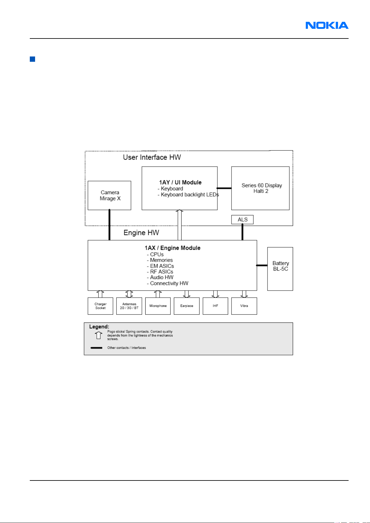
Baseband description
System module block diagram
The device consists of two different main modules: transceiver (1ax) and UI (1ay). The transceiver board consists
of baseband and RF components
The UI board consists of key domes and keypad backlights. Connection between the UI and the transceiver board
is established via a board-to-board spring connector.
Note: In this description, user interface HW covers display, camera, keyboard, keyboard backlight and
ALS.
Figure 90 System level block diagram
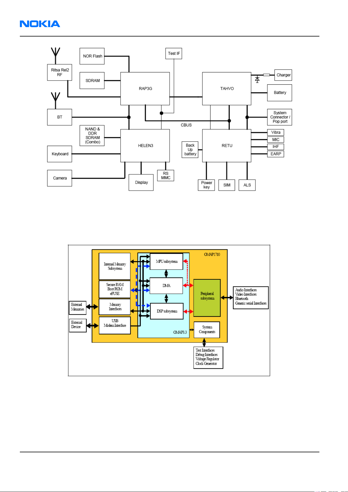
Baseband functional description
Digital baseband consists of ISA based modem and SYMBIAN based application sections. Modem functionality
is in RAP3G and Helen2/3 acts as a platform for SYMBIAN applications.
Modem section consists of RAP3G ASIC with NOR FLASH and SDRAM memory as the core. RAP3G supports cellular
protocols of WCDMA (3GPP R-4) and GSM (minimum EDGE glass 10, GPRS phase2). Modem SDRAM memory have
64Mbits of memory and NOR flash have 64Mbits of memory. RAP3G operates with the system clock of 38.4 MHz,
which comes from the VCTCXO.
Application section includes Helen3 ASIC with DDR/NAND combo memory as the core. Stacked DDR/NAND
application memory has 256Mbits of DDR memory and 256Mbits of flash memory. Helen3 uses 19.2MHz clock,
which comes from the RAP3G divided by two from the 38.4 MHz system clock.
Issue 1 Company Confidential Page 9–7
Copyright © 2004 Nokia. All Rights Reserved.
Page 8
RM-1
Nokia Customer Care System Module
Figure 91 Functional block diagram
Helen3 processor (OMAP1710) is called also as an application ASIC in RM-1 because it is processing application
SW and handles the UI SW. It consists of OMAP3.3 and peripheral subsystems like camera-, display- and keyboard
driver blocks.
Figure 92 Helen3 high level block diagram
OMAP3.3 consists of ARM926 (MPU subsystem), TMS320C55x (DSP subsystem), DMA and OMAP3.3s internal
peripherals.
Helen3s MPU subsystem is based on an ARM926EJ. MPU is able to perform most of the application operations
on the chip.
System DMA: This component is mainly used to help the MPU and DSP perform data memory transfer-specific
tasks, leaving more available MIPS for both processors.
Page 9–8 Company Confidential Issue 1
Copyright © 2004 Nokia. All Rights Reserved.
Page 9
RM-1
System Module Nokia Customer Care
The DSP subsystem is based on a TMS320C55x™ DSP core, which is responsible for intensive data computing
tasks like real-time audio and video handling on application side. E.g. voice recording.
Internal memory subsystem: This subsystem is composed of a single port SRAM.
Secure modules: OMAP1610 contains a set of several components, including ROM, a single port SRAM, and eFUSE
cells. These components enable the system to support secure applications.
Memory interfaces: The memory interfaces define the system memory access organization of OMAP1610.
USB & modem interface: These two modules enable the platform to support a universal serial link and a
dedicated modem interface, enabling a high data transfer rate between the modem and the application chip.
System components: System components are group of modules responsible for managing system interactions
such as interrupt, clock control and idle.
Peripheral subsystem: The peripheral subsystem defines all the components used to interface OMAP1610 with
specific external devices such as camera, keyboard, display etc.
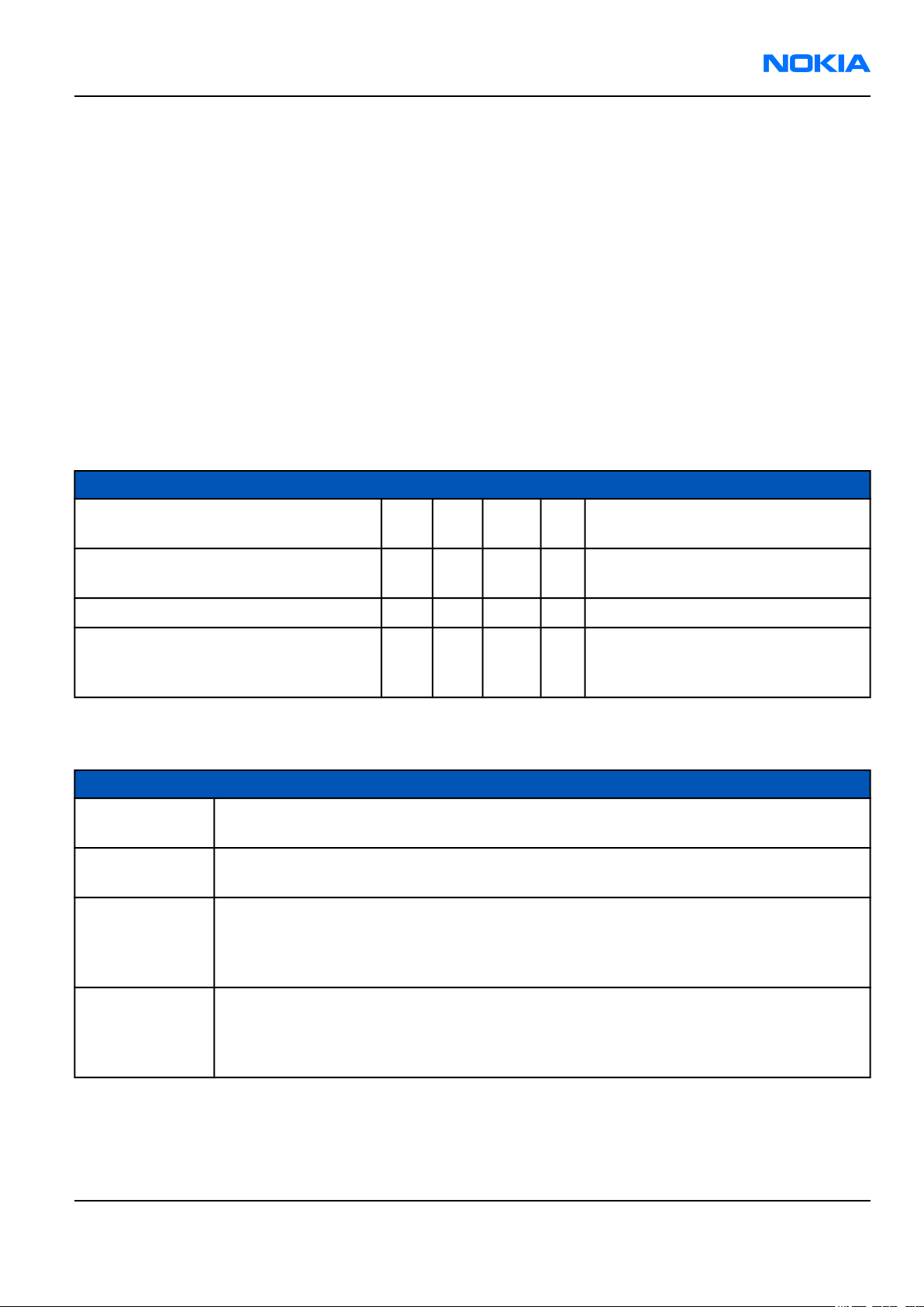
Absolute maximum ratings
Signal Min Nom Max Unit Notes
Battery voltage (idle) -0.3 +4.5 V Battery voltage maximum value is
specified during charging is active
Battery voltage (Call) +4.3 V Battery voltage maximum value is
specified during charging is active
Charger input voltage -0.3 +16V V
Back-Up supply voltage 0 2.5 2.7 V Maximum capacity of the backup
power supply assumed to be 200
µAh.
Modes of operation
Mode Description
NO_SUPPLY (dead) mode means that the main battery is not present or its voltage is too low (below
RETU master reset threshold) and that the back-up battery voltage is too low.
BACK_UP The main battery is not present or its voltage is too low but back-up battery voltage is
adequate and the 32kHz oscillator is running (RTC is on).
PWR_OFF In this mode (warm), the main battery is present and its voltage is over RETU master reset
threshold. All regulators are disabled, PurX is on low state, the RTC is on and the oscillator
is on. PWR_OFF (cold) mode is almost the same as PWR_OFF (warm), but the RTC and the
oscillator are off.
RESET RESET mode is a synonym for start-up sequence. In this mode certain regulators are
enabled and after they and RFClk have stabilized, the system reset (PurX) is released and
PWR_ON mode entered. RESET mode uses 32kHz clock to count the REST mode delay
(typically 16ms).
Issue 1 Company Confidential Page 9–9
Copyright © 2004 Nokia. All Rights Reserved.
Page 10

RM-1
Nokia Customer Care System Module
Mode Description
SLEEP SLEEP mode is entered only from PWR_ON mode with the aid of SW when the system’s
activity is low. There are in principle three different sleep modes:
• Helen3 sleep
• RAP3G sleep
• Helen3 and RAP3G sleep (deep sleep)
In SLEEP mode RETU’s regulators VIO, VDRAM, VSIM1, VSIM2, VAUX and Vana are in low
quiescent current mode (output voltages still present but regulators will not give as much
current out). Other regulators including VR1 supplying system clock oscillator are
disabled.
In SLEEP mode, TAHVO VCORE SMPS regulator is in low quiescent current mode (if sleep
mode is not internally disabled). Linear regulator VOUT state depends on the accessory
connected to the system connector (Pop-Port), if there is any.
FLASHING FLASHING mode is for SW downloading. FLASHING mode is not really a RETU or TAHVO
state but rather a system state. From RETU and TAHVO point of view, it is like PWR_ON.
The state is entered from PWR_ON. It is possible to use external voltage (VPP) during
flashing to speed up the process (provided that the memory components support the
feature).
Page 9–10 Company Confidential Issue 1
Copyright © 2004 Nokia. All Rights Reserved.
Page 11
RM-1
System Module Nokia Customer Care
Figure 93 State diagram
Voltage limits
Parameter Description Value
VMSTR Master reset threshold (RETU) 2.2V (typ.)
Threshold for charging, rising
VMSTR+
VMSTR-
VCOFF+ Hardware cutoff (rising) 2.9V (typ.)
VCOFF- Hardware cutoff (falling) 2.6V (typ.)
SWCOFF SW cutoff limit ~3.2V
Issue 1 Company Confidential Page 9–11
(TAHVO) 2.1V (typ.)
Threshold for charging, falling
(TAHVO) 1.9V (typ.)
Copyright © 2004 Nokia. All Rights Reserved.
Page 12
RM-1
Nokia Customer Care System Module
The master reset threshold controls the internal reset of Retu / (Tahvo). If battery voltage is above VMSTR, UEME’s
charging control logic is alive. Also, RTC is active and supplied from the main battery. Above VMSTR UEME allows
the system to be powered on although this may not succeed due to voltage drops during start up. SW can also
consider battery voltage too low for operation and power down the system.
Power key
The system boots up when power key is pressed (adequate battery voltage, VBAT, present).
Power down can be initiated by pressing the power key again (the system is powered down with the aid of
SW). Power on key is connected to Retu ASIC via PWRONX signal.
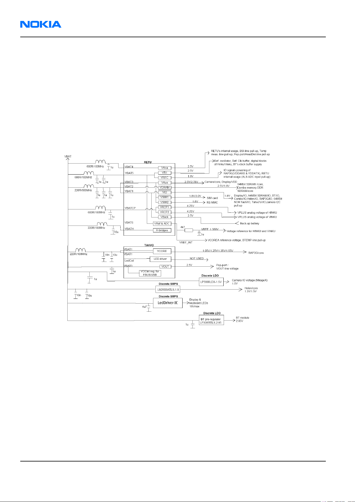
Power distribution
Figure 94 Power distribution diagram
Power supply components:
• RETU
• TAHVO
• Helen VCORE SMPS
• BT
• LDO
• camera LDO
• backlight SMPS
All the above are powered by the main battery voltage.
Battery voltage is also used on the RF side for power amplifiers (GSM PA & WCDMA PA) and for RF ASICs Hinku
(Rx) & Vinku(Tx).
Page 9–12 Company Confidential Issue 1
Copyright © 2004 Nokia. All Rights Reserved.
Page 13

RM-1
System Module Nokia Customer Care
Discrete power supplies are used to generate 2.8V for BT, 1.5V for the camera module, 1.3V/1.5V for Helen3 and
18V for backlight LEDs.
The device supports both 1.8V/3V SIM cards which are powered by RETU / VSIM1. RETUs VSIM2 is used to power
RS MMC 1.8V only. USB accessories which needs power from the device are powered by TAHVO / VOUT.
Because LED driver in TAHVO is not used, the external SMPS is used instead. External LED SMPS is still controlled
by TAHVO and powered by battery voltage.
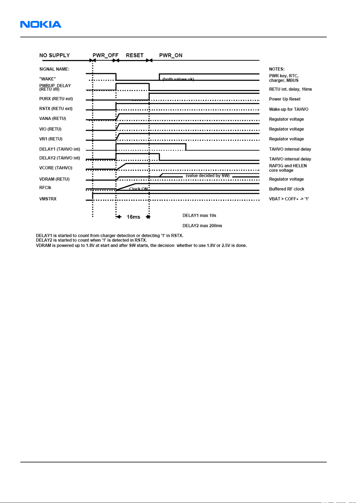
System power-up
After inserting the main battery, regulators started by HW are enabled. SW checks, if there is some reason to
keep the power on. If not, the system is set to power off state by watchdog. Power up can be caused by the
following reasons:
• Power key is pressed
• Charger is connected
• RTC alarm occurs
• MBUS wake-up
After that:
• Retu activates sleep clock and VANA, VDRAM, VIO and VR1 regulators.
• Voltage appearing at Retu’s RSTX pin is used for enabling Tahvo ASIC.
• Tahvo enables VCORE regulator and its internal RC-oscillator (600kHz).
• VCTCXO regulator is set ON and RF clock (main system clock) is started to produce.
• Retu will release PURX ~ 16ms after power up is enabled (the RF clock is then stable enough).
• Synchronizing clock (2.4MHz) for Tahvo is started to be produced. After PURX is released and two rising edges
of 2.4MHz synchronous clock have been detected in SMPSClk input Tahvo is starting to use that instead of
600kHz internal RC-oscillator.
• HW start-up procedure has been finalized and the system is up and running. Now it is possible for SW to
switch ON other needed regulators.
Issue 1 Company Confidential Page 9–13
Copyright © 2004 Nokia. All Rights Reserved.
Page 14
RM-1
Nokia Customer Care System Module
Figure 95 System start-up timing
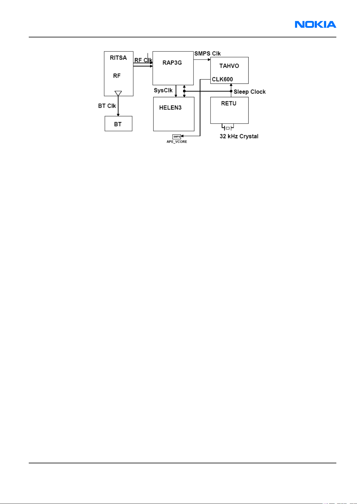
Clocking scheme
In BB5.0, two main clocks are provided to the system: 38.4MHz RF clock produced by VCTCXO in RF section and
32.768kHz sleep clock produced by RETU with an external crystal.
RF clock is generated only when VCTCXO is powered on by RETU regulator. Regulator itself is activated by SleepX
signals from both RAP3G and Helen3. When both CPUs are on sleep, RF clock is stopped.
RF clock is used by RAP3G that then provides (divided) 19.2MHz SysClk further to Helen3. Both RAPG and Helen3
have internal PLLs which then create clock signals for other peripheral devices/interfaces like RS MMC, SIM, CCP,
I2C and memories.
32k Sleep Clock is always powered on after startup. Sleep clock is used by RAP3G and Helen3 for low-power
operation.
SMPS Clk is 2.4MHz clock line from RAP3G to Tahvo used for switch mode regulator synchronizing in active
mode. In deep sleep mode, when VCTCXO is off, this signal is set to '0'-state.
BT Clk is 38.4MHz signal from Hinku ASIC to BT module.
CLK600 is 600KHz signal from Tahvo to APE VCORE SMPS. The clock source is internal RC oscillator in Tahvo (during
the RM-1 power-up sequence) or RAP3G SMPS Clk divided by 4 after the power-up sequence.
Page 9–14 Company Confidential Issue 1
Copyright © 2004 Nokia. All Rights Reserved.
Page 15
RM-1
System Module Nokia Customer Care
Figure 96 Clocking scheme
Bluetooth
Bluetooth provides a fully digital link for communication between a master unit and one or more slave units.
The system provides a radio link that offers a high degree of flexibility to support various applications and
product scenarios. Data and control interface for a low power RF module is provided. Data rate is regulated
between the master and the slave.
The device Bluetooth is based on CSR's BC3 BT ASIC.
The UART1 interface handles the transfer of control and data information between Helen3 and the BT system
(BC3).
The PCM interface is used for audio data transfer between RAP3G and the BT system (BC3).
USB
USB (Universal Serial Bus) provides a wired connectivity between host PC and peripheral devices.
USB is a differential serial bus for USB devices. USB controller (RAP3G) supports USB specification revision 2.0
with full speed USB (12Mbps). The device is connected to the USB host through the Pop-PortTM connector. The
USB bus is hot plugged capable, which means that USB devices may be plugged in/out at any time.
See Also
• USB interface electrical characteristics (Page 9–29)
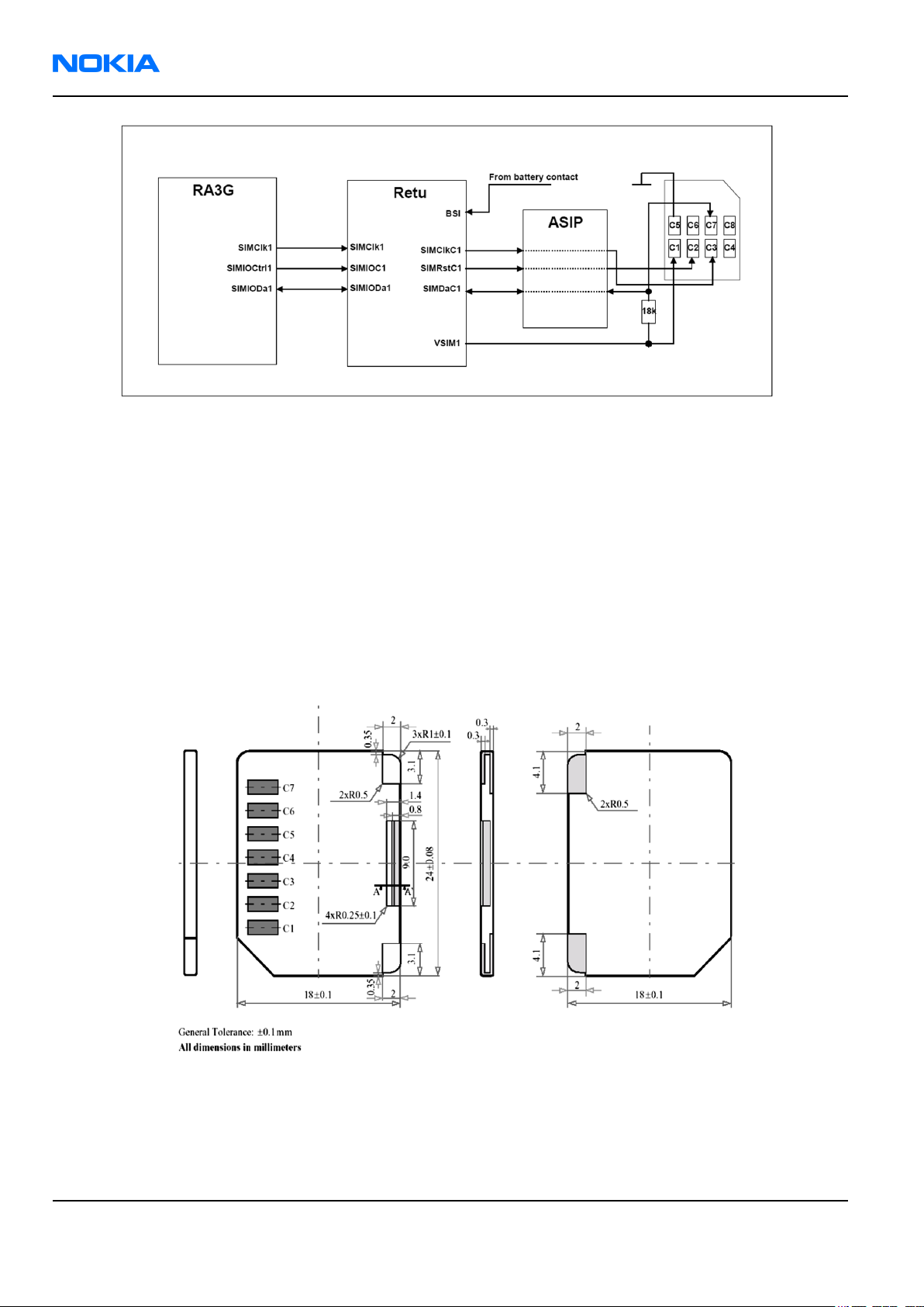
SIM interface
The device has one SIM (Subscriber Identification Module) interface and the SIM card location is under the
battery. SIM interface consists of internal interface between RAP3G and Retu and an external interface between
Retu and SIM contacts. SIM interface functionality is located in RAP3G while Retu takes care of power up/down,
card detection, ATR counting and level shifting. For Retu external SIM IF connections, see SIM interface
connections (Page 9–31).
The SIM IF is shown in the following figure:
Issue 1 Company Confidential Page 9–15
Copyright © 2004 Nokia. All Rights Reserved.
Page 16
RM-1
Nokia Customer Care System Module
Figure 97 SIM interface
Retu handles SIM card detection and the detection method is based on the BSI line. Due to location of the SIM
card removal of the battery causes quick power down of the SIM IF. The Retu SIM1 interface supports both the
1.8V and 3.0V SIM cards. SIM interface voltage is first 1.8V when the SIM card is inserted and if the card does not
response to the ATR (Answer To Reset) 3V interface voltage is used. The data communication between the card
and the phone is asynchronous half duplex and the clock supplied to cards is 1-5MHz, which is 3.2MHz by default
(in GSM system). The data baud rate is SIM card clock frequency divided by 372 (by default), 64, 32 or 16.
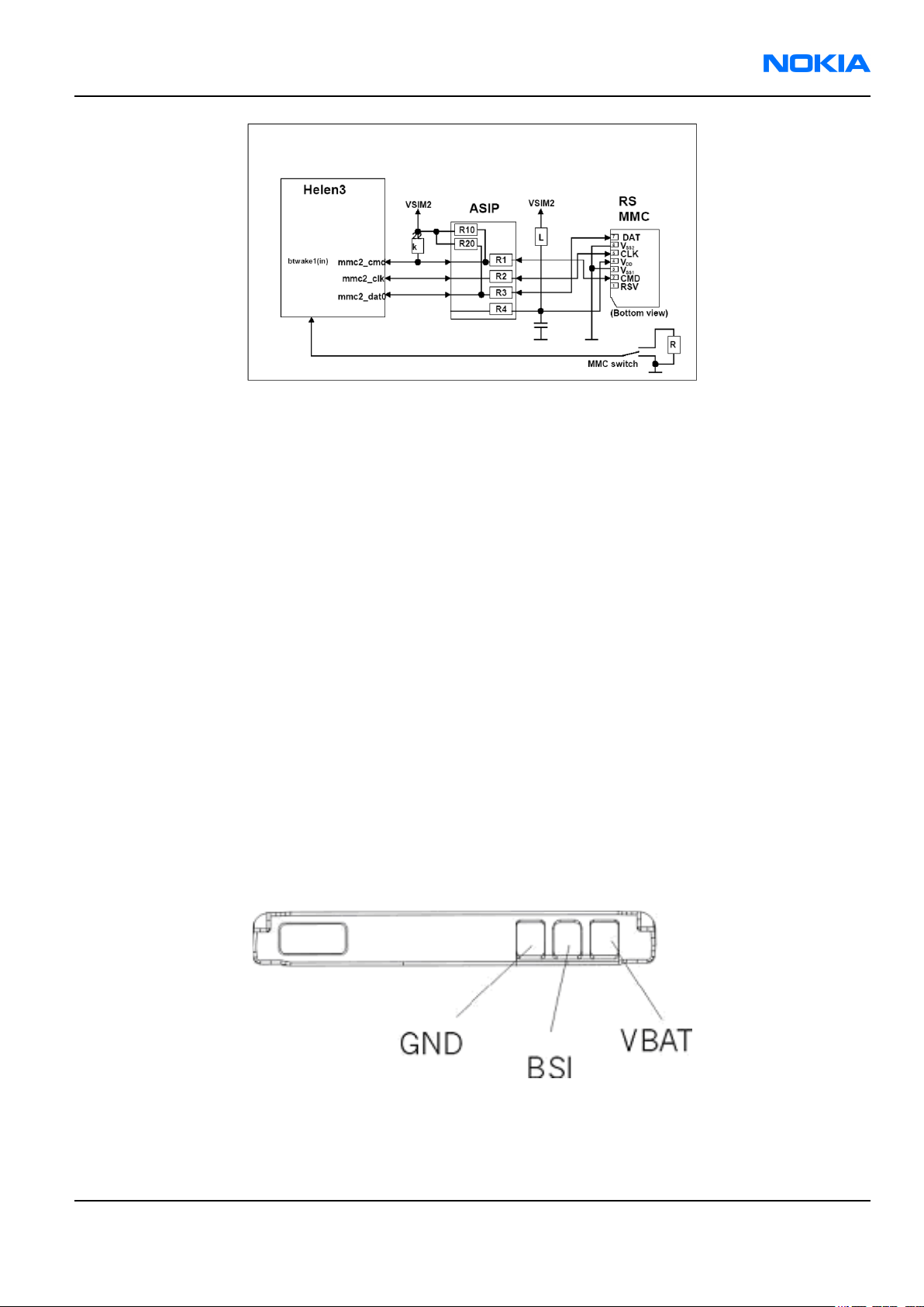
RS MMC interface
The reduced size (24mm x 18mm x 1.4mm) multimedia card slot is located under the battery. The device
supports RS MMC hot insertion so it is possible to remove/insert the card when the phone is powered on.
Figure 98 Reduced size MMC
RS MMC card is connected to the Helen3 processor MMC/SDIO2 (1.8V) interface. MMC interface is shown in the
following figure:
Page 9–16 Company Confidential Issue 1
Copyright © 2004 Nokia. All Rights Reserved.
Page 17
RM-1
System Module Nokia Customer Care
Figure 99 MMC interface
The basic multimedia card concept is based on the following communication signals CLK, CMD and DAT. With
each cycle of the CLK signal one bit transfer on the DAT and CMD line is done. The maximum CLK frequency is
20MHz (specified in multimedia card specification). Maximum used CLK frequency at the time is 16MHz. CMD is
a bi-directional command channel used for card initialization and data transfer commands. CMD signal has two
operational modes open-drain and push-pull mode. Open-drain mode is used for card initialization and pushpull mode for fast command transfer. CMD commands are sent by the host and CMD responses are sent by the
card. DAT is a bi-directional data channel, which operates at push-pull mode.
The detection of RS MMC card removal/insertion is done via RS MMC cover switch. Removing RS MMC while writing
to RS MMC may corrupt data in RS MMC. RS MMC cover switch gives an interrupt to the SW while the cover is
opened or closed. After RS MMC cover lid opening (RS MMC SW signal is connected to GND via cover switch) the
SW power down the RS MMC card and switches off the RS MMC power supply (VSIM2). When the RS MMC cover
lid is closed (RS MMC SW signal is internally connected in Helen3 to 1.8V) the card should be identified if card
exists.
See Also
• RS MMC interface connections (Page 9–31)
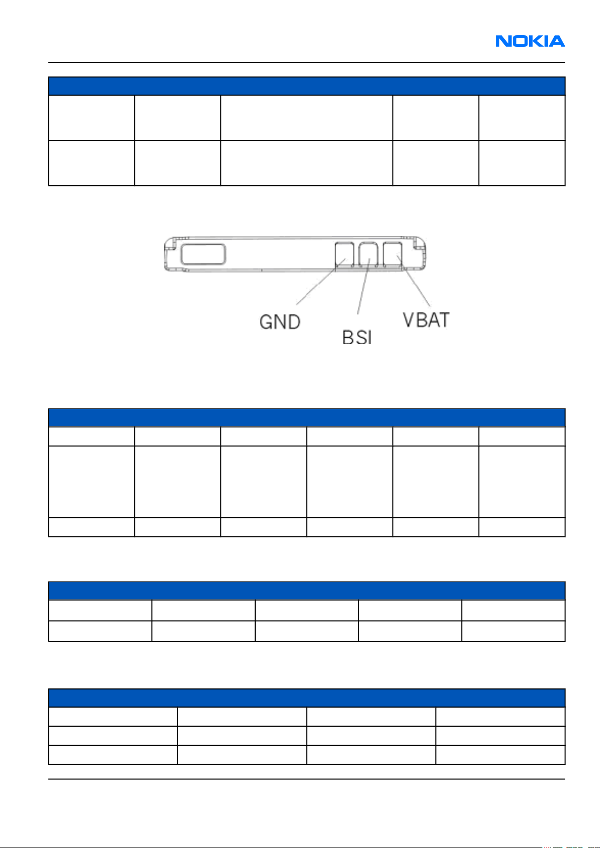
Battery interface
The battery interface supports NMP Lynx battery interface for the BL-5C battery. This interface consists of three
connectors: VBAT, BSI and GND. BSI line is used to recognize battery capacity by a battery internal pull down
resistor.
Figure 100 Battery pin order
Battery temperature is estimated by measuring separate battery temperature NTC via BTEMP line, which is
located on the transceiver PWB, in a place where phone temperature is most stabile.
Issue 1 Company Confidential Page 9–17
Copyright © 2004 Nokia. All Rights Reserved.
Page 18

RM-1
Nokia Customer Care System Module
For service purposes the device SW can be forced into local mode by using pull down resistors connected to the
BSI line.
See Also
• Battery connector and interface connections & electrical characteristics (Page 9–33)
Camera interface
The device uses a Mirage- X camera module. Mirage-X is a 1.3Mpixel camera with sensor resolution of 1280 x
960. The following figure shows the block diagram where CCP bus is used to transfer image data from camera
to engine. Bi-directional control bus is an SW implemented I2C interface.
Camera regulator N1470 powers digital parts of camera. VAUX power rail is for powering analogue parts of the
camera.
CAMVCTRL signal (Vctrl) is used for activating the camera module. When Vctrl is turned on High level , the camera
module enters the operation mode. When Vctrl is turned on Low level, the camera module enters the power
off mode.
CAMCLK signal feeds system clock for camera module.
Figure 101 Block diagram of Mirage-X camera module
See Also
• Camera interface connections and electrical characteristics (Page 9–37)
Page 9–18 Company Confidential Issue 1
Copyright © 2004 Nokia. All Rights Reserved.
Page 19

RM-1
System Module Nokia Customer Care
User interface
Display interface
Display module mechanical concept
Figure 102 General diagram of the LCD module
Display features:
• 65536 colours
• Partial display function Power saving by pausing display process on part of the screen.
• Built-in RAM capacity 176rows×208lines×16bit = 585,728 bits
The display has two different operating modes:
1 Normal mode, Full screen, 65k colours
2 Normal Partial mode, 65k colors but only part of the display is active
The module includes:
• FPWB foil including connector and discretes and driver circuits
• display panel (glass)
• drivers including display controller and 176 x 208 x 16 bits RAM
• backlight system: lightguide, LEDs and necessary optical sheets
• supporting mechanics
• metal frame (stainless steel)
• plastic frame
The interconnection between the LCD module and the Nokia engine is implemented with a 24-pin board-toboard connector.
Display is controlled via MeSSi-8 interface by Helen3. All MeSSi-8 signals go through the EMC filtering ASIPs.
The display module does not require any tunings in service.
Issue 1 Company Confidential Page 9–19
Copyright © 2004 Nokia. All Rights Reserved.
Page 20

RM-1
Nokia Customer Care System Module
Keyboard
The device keyboard is connected to the main PWB with a board-to-board connector.
The keymatrix has six rows and four columns. The voice key on the main PWB and the navigation key are
connected to the same keymatrix.
Table 7 Keymatrix
Col3 Col2 Col1 Col0
Row0 Right Left Right soft key Left soft key
Row1 Down Up Send Select
Row2 8 3 2 7
Row3 6 1 5
Row4 # * 9
Row5 4 Voice End
Row6 Apps Clear Edit 0
Display and keyboard backlight
The device has one Led Driver (SMPS) that is used to drive both display and keyboard LEDs.
Both display LEDs (4pcs) and keyboard LEDs (4pcs) are connected in series.
Current adjustment of the driver is done from the display LED branch, and keyboard current also depends on
the display brightness.
In a typical use case, keyboard LEDs are turned ON only in dark ambient lighting conditions.
Control signals for LED driver are:
From To Voltage Function
GenOut1 TAHVO R2302 (10k) 0V / 1.8V Maximum current
GenOut2 TAHVO R2301 (4k7) 0V / 1.8V
PWM TAHVO J2309, N2301 PWM 0%-100%,
1.8V
GenOut3 TAHVO V2300 0V / 1.8V Keyboard LEDs ON
control (0V ->max
curr.)
Current PWM
control (16 steps)
(1.8V) /OFF (0V)
ALS interface
Ambient Light Sensor (ALS) is located in the upper part of the phone. It consists of a lightguide (part of front
cover), phototransistor (V4400)+ resistor (R4401), NTC + resistors (R4400, R4402, R4403) and RETU EM ASIC
(N2200). Information of ambient lighting is used to control backlights of the phone:
• Keypad lighting is switched on only when environment is dark / dim
• Display backlights are dimmed, when environment is dark / dim
Ambient light sensor itself is a photo transistor which is temperature-compensated by an external NTC resistor.
Retu with its ADC reads the light sensor (LS) and temperature (LST) results.
Page 9–20 Company Confidential Issue 1
Copyright © 2004 Nokia. All Rights Reserved.
Page 21

RM-1
System Module Nokia Customer Care
ALS calibration is not possible in the service points. It is replaced by using selected phototransistors as spare
parts.
Figure 103 ALS HW implementation
Table 8 ALS resistor values
Symbol R1 R2 R3 R4 R5 R6 R7 NTC-res
Value 5 kOhm 15 kOhm 30 kOhm 50 kOhm
470
kOhm
100
kohm
470
kohm 47 kOhm
ASICs
RAP3G ASIC
RAP3G ASIC is a 3G Radio Application Processor. RAM memory is integrated into RAP3G.
In general RAP3G consists of three separate parts:
• Processor subsystem (PSS) that includes the main processor and related functions
• MCU peripherals that are mainly controlled by MCU
• DSP peripherals that are mainly controlled by DSP
RAP3G core voltage (1.40V) is generated from Tahvo VCORE and I/O voltage (1.8V) is from Retu VIO. The core
voltage in sleep mode is lowered to 1.05V.
Retu EM ASIC
Retu EM ASIC includes the following functional blocks:
• Start up logic and reset control
• Charger detection
• Battery voltage monitoring
• 32.768kHz clock with external crystal
• Real time clock with external backup battery
• SIM card interface
• Stereo audio codecs and amplifiers
• A/D converter
• Regulators
Issue 1 Company Confidential Page 9–21
Copyright © 2004 Nokia. All Rights Reserved.
Page 22

RM-1
Nokia Customer Care System Module
• Vibra interface
• Digital interface (CBUS)
Tahvo EM ASIC
Tahvo EM ASIC includes the. following functional blocks:
• Core supply generation
• Charge control circuitry
• Level shifter and regulator for USB/FBUS
• Current gauge for battery current measuring
• External LED driver control interface
• Digital interface (CBUS)
Device memories
RAP3G memories NOR flash and SDRAM
Modem memory consists of 64 Mbit SDRAM and 64 Mbit NOR flash memories.
SDRAM is a dynamic memory for ISA SW.
NOR is used for ISA SW code and PMM data and CDSP SW code.
16-bit wide SDRAM interface consists of DDR SDRAM controller from ARM, DCDL/DLLs and wrapper logic. 32-bit
wide flash interface is implemented by using EMC module.
SDRAM core voltage (1.8V) is generated from Retu VDRAM and I/O voltage (1.8V) is from VIO. NOR flash uses VIO
for both core and I/O voltages.
Combo memory (Helen 3)
The application memory of the device consists of NAND/DDR combo memory. Stacked DDR/NAND application
memory has 256 Mbit of DDR memory and 256 Mbit of flash memory. DDR DRAM memory is stacked above the
NAND flash.
Helen 3 includes a 16-bit dedicated memory interface called external memory interface fast (EMIFF). This is used
to support interface for DDR memory. OMAP1610 provides also NAND flash controller located on the shared
peripheral bus, providing support for 8-bit NAND flash. The interface requires an 8-bit address bus multiplexed
with 8-bit data bus and several control signals.
Core voltage for DDR is 1.8V, which is generated by discrete LDO (LP3999-1.8). 1.8V (VIO) is for DDR I/O voltage.
Both NAND core and I/O voltages are 1.8V generated by VIO.
Audio concept
Audio HW architecture
The functional core of the audio hardware is built around two ASICs: RAP 3G CMT engine ASIC and the mixedsignal ASIC Retu.
Retu provides an interface for the transducers and the accessory connector. Because audio amplifiers are also
integrated into Retu, the only discrete electronics components needed for audio paths are audio filtering
components and EMC/ESD components.
There are three audio transducers:
• 8mm dynamic earpiece
Page 9–22 Company Confidential Issue 1
Copyright © 2004 Nokia. All Rights Reserved.
Page 23

RM-1
System Module Nokia Customer Care
• 16mm dynamic speaker
• electret microphone module
In addition to the audio transducers, Retu also provides an output for the dynamic vibra component.
All galvanic audio accessories are connected to the Pop-PortTM accessory connector.
A Bluetooth audio module BC02 that is connected to RAP3G supports Bluetooth audio functionality.
There is a separate application ASIC, Helen 2 (OMAP 1610) for Symbian applications.
Figure 104 Audio block diagram
Internal microphone
Internal microphone is used for HandPortable (HP) and Internal HandsFree (IHF) call modes.
An analogue electret microphone is connected to Retu ASIC’s Mic1P and Mic1N inputs via asymmetric electrical
connection.
The microphone is biased by Retu ASIC MicB1 bias voltage output.
Issue 1 Company Confidential Page 9–23
Copyright © 2004 Nokia. All Rights Reserved.
Page 24

RM-1
Nokia Customer Care System Module
Figure 105 Internal microphone circuitry
External microphone
Galvanic accessories are connected to the system connector (Pop-PortTM).
Accessory audio mode is automatically enabled/disabled during connection/disconnection of dedicated phone
accessories.
External microphone circuitry is biased by Retu ASIC MicB2 bias voltage output. The circuitry provides a
symmetrical connection for the microphone from the Pop-PortTMconnections, XMICN and XMICP, to Retu ASIC
inputs, Mic2P and Mic2N.
Figure 106 External microphone circuitry (Pop-Port connects to the right side)
Internal earpiece
Internal earpiece is used for the HandPortable (HP) call mode. A dynamic 8mm earpiece capsule is connected
to Retu ASIC’s differential output EarP and EarN.
Page 9–24 Company Confidential Issue 1
Copyright © 2004 Nokia. All Rights Reserved.
Page 25

RM-1
System Module Nokia Customer Care
Figure 107 Internal earpiece circuitry
Internal speaker
Internal speaker is used for Internal HandsFree (IHF) call mode.
A dynamic 16mm speaker is connected to Retu ASIC’s outputs HFSpP and HFSpN.
IHF amplifier integrated in Retu is a Digital Pulse Modulated Amplifier (DPMA).
Figure 108 Internal speaker circuitry
External earpiece
Galvanic accessories are connected to the system connector (Pop-PortTM).
Accessory audio mode is automatically enabled/disabled during connection/disconnection of dedicated phone
accessories.
Retu ASIC provides two output channels in either single-ended or differential format. Retu ASIC outputs XearL
and XearLC form the left channel audio output and XearR and XearRC the right channel audio output. XearLC
and XearRC are the ground pins if the output works in a single-ended operation.
On the Pop-Port side, HSEAR P and HSEAR N form the left channel output and HSEAR R P and HSEAR R N the right
channel output. Respectively, HSEAR N and HSEAR R N are the ground pins if the output works in a single-ended
operation.
Issue 1 Company Confidential Page 9–25
Copyright © 2004 Nokia. All Rights Reserved.
Page 26

RM-1
Nokia Customer Care System Module
Figure 109 External earpiece circuitry (Pop-Port connected on the right)
Vibra circuitry
Vibra is used for vibra-alarm function.
The vibra motor is connected to the Retu ASIC VibraP and VibraN Pulse Width Modulated (PWM) outputs.
Figure 110 Vibra circuitry
Pop-portTM connector
Pop-PortTM connector provides a fully differential 4–wire connection.
The HandsFree (HF) driver in Retu is meant for the headset.
The output is driven in a fully differential mode. In the fully differential mode, the HF pin is the negative output
and the HFCM pin is the positive output. The gain of the handsfree driver in the differential mode is 6 dB.
The earpiece (EARP, EARN) and headset (HF, HFCM) signals are multiplexed so that the outputs cannot be used
simultaneously.
Page 9–26 Company Confidential Issue 1
Copyright © 2004 Nokia. All Rights Reserved.
Page 27
RM-1
System Module Nokia Customer Care
The HF and HFCM amplifiers include a transient suppression circuitry, which prevents undesired spikes in XEarL
and XEarLC outputs when switching on and off the amplifiers. The HeadInt line is pulled up to 2.7V by the internal
resistor when the accessory is connected. When there is not accessory inserted, the voltage in the HeadInt line
will be <0.8 V caused by internal pull down resistor in the HF line.
Figure 111 External audio connector
Table 9 Audio connector pin assignments
Pin #/ Signal
name
1/ Charge V Charge DC 0-9V/ 0.85A
2/ GND Charge GND - 0.85A 100mW (PWB+
3/ ACI ACI 1kbits/s Digital 0 / 47W Insertion &
4/ Vout DC out DC 2.78V 70 mA 100mW (PWB+
9 / XMIC N Audio in 300-8k 1Vpp &
10 / XMIC P Audio in 300-8k 1Vpp &
11 / HEAR N Audio out 20-20k 1Vpp 10W
12 / HEAR P Audio out 20-20k 1Vpp 10W
Signal
description
Spectral range Voltage/
Current levels
2.5-2.78V
2.5V 90mA
2.5-2.78VDC
2.5-2.78VDC
Max or nominal
serial
impedance
conn.)
conn.)
Notes
removal
detection
200mW
13 / HEAR R N Audio out 20-20k 1Vpp 10W Not conn. in
mono
14 / HEAR R P Audio out 20-20k 1Vpp 10W Not conn. in
mono
Issue 1 Company Confidential Page 9–27
Copyright © 2004 Nokia. All Rights Reserved.
Page 28

RM-1
Nokia Customer Care System Module
Baseband technical specifications
External interfaces
Name of Connection Connector reference Material Code
USB X2001 5460061
Charger X2000 5400243
Headset X2001 5460061
SIM X2700 N/A
RS MMC X5200 5469301
Battery connector X2070 5409255
ACI interface electrical characteristics
Description Parameter Min Typ Max Unit Notes
Accessory detection
Headset
1.75 1.9 2.05 V Retu specific
detection
threshold
Headset
25 mV
detection
hysteresis
Headset
1 2 4 uA
detection
pull ups
After Mbus is switched to HeadDet
High-level
input
V
IH
0.7 x V
DDS
V
DDS
V RAP3G
specific
voltage
(VDDS = 1.8V)
Low-level
V
IL
0 0.3 x V
DDS
V
input
voltage
High-level
V
OH
0.8 x V
DDS
V
DDS
V
output
voltage
Low-level
V
OL
0 0.22 x VDDS V
output
voltage
Rise/fall
tR/tF
25 ns
time
Page 9–28 Company Confidential Issue 1
Copyright © 2004 Nokia. All Rights Reserved.
Page 29

RM-1
System Module Nokia Customer Care
VOUT electrical characteristics
Description Parameter Min Max Unit Notes
Vout regulator
VOUT 2.43 2.57 V Max load 90mA
for external
accessories
USB IF electrical characteristics
Description Parameter Min Max Unit Notes
Absolute
maximum
voltage on D+
and D-
Supply voltage VBUS 4.4 5.25 V
Supply current:
Functioning I
Suspended I
Unconfigured I
High-level
input voltage:
V
VBUS
VBUS
VBUS
D+/D-
-1 4.6 V USB
specification
revision 2.0
100 mA
500 uA
100 mA
V
High (driven) V
High (floating) V
Low-level input
voltage
Differential
input
sensitivity
Differential
input voltage
range
Low-level
output voltage
High-level
output voltage
(driven)
Output signal
crossover
voltage
IH
IHZ
V
IL
V
DI
V
CM
2
2.7 3.6
0.8 V
0.2 V |(D+) - (D-)|
0.8 2.5 V Included VDI
range
V
OL
V
OH
V
CRS
0 0.3 V
2.8 3.6 V
1.3 2 V
Issue 1 Company Confidential Page 9–29
Copyright © 2004 Nokia. All Rights Reserved.
Page 30

RM-1
Nokia Customer Care System Module
FBUS interface electrical characteristics
Description Parameter Min Typ Max Unit Notes
High-level
input
V
IH
0.7 x
V
DDSHV2
V
DDSHV2
V Helen2/3 specific
voltage
(VDDSHV2 =
1.8V)
Low-level
Input
V
IL
0 0.3 x
V
DDSHV2
V
voltage
High-level
output
V
OH
0.8 x
V
DDSHV2
V
DDSHV2
V
voltage
Low-level
output
V
OL
0 0.22 x
V
DDSHV2
V
voltage
Rise/fall
tR/tF
0 25 ns
time
Headset hook detection interface (XMICN) electrical characteristics
Description Min Typ Max Unit Notes
Hook detection
threshold 1
Hook detection
threshold 2
Hook detection
1.25 1.35 1.45 V Two fixed
thresholds
0.5 0.6 0.7 V
inside Retu.
Selectable by
SW
25 mV
hysteresis
Hook detection
1 2 4 uA
pull ups
Audio signal electrical characteristics
Description Parameter Min Typ Max Unit Notes
XMIC N Audio in 1 V
XMIC P Audio in 1 V
HSEAR N Audio out 1 V
pp
pp
pp
DC Offset 2.5-
2.78V
DC Offset 2.5-
2.78V
10Ω nominal
serial
impedance
Page 9–30 Company Confidential Issue 1
Copyright © 2004 Nokia. All Rights Reserved.
Page 31

RM-1
System Module Nokia Customer Care
Description Parameter Min Typ Max Unit Notes
HSEAR P Audio out 1 V
pp
10Ω nominal
serial
impedance
HSEAR R N Audio out 1 V
pp
10Ω nominal
serial
impedance
Not
connected in
mono
HSEAR R P Audio out 1 V
pp
10Ω nominal
serial
impedance
Not
connected in
mono
SIM IF connections
Pin Signal I/O Engine connection Notes
C1 VSIM Out Retu VSIM1 Supply voltage
to SIM card,
1.8V or 3.0V.
C2 SIMRST Out Retu SIM1Rst Reset signal to
SIM card
C3 SIMCLK Out Retu SIM1ClkC Clock signal to
SIM card
C5 GND - GND Ground
C7 SIMDATA In/Out Retu SIM1DaC Data input /
output
RS MMC interface connections
Pin Signal I/O Engine connection Notes
1 RSV NC NC Reserved for
future use
2 CMD <-> Helen2/3 MMC2_CMD Command/
Response
3 Vss1 GND Ground
4 V
DD
<- Retu VSIM2 VSIM2, supply
voltage 1.8
(Max 70mA)
Issue 1 Company Confidential Page 9–31
Copyright © 2004 Nokia. All Rights Reserved.
Page 32
RM-1
Nokia Customer Care System Module
Pin Signal I/O Engine connection Notes
5 CLK <- Helen2/3 MMC2_CLK External clock
for the MMC
card, Max 20
MHz
6 Vss2 GND Ground
7 DAT <-> Helen2/3 MMC2_DAT0 Bi-directional
data bus
- MMCDET -> Helen2/3 btwake1(in)
[P10]
MMC card
detect
Charger connector and charging interface connections & electrical characteristics
Figure 112 Charger connector
Table 10 Charging interface connections
Pin Signal I/O Engine connection Notes
1 Vchar In Tahvo VCharIn1, 2 Charging
voltage /
charger
detection,
Center pin
2 Charge GND Ground Charger ground
Table 11 Charging IF electrical characteristics
Description Parameter Min Max Unit Notes
Vchar V Charge 0 9 V Center pin
Vchar I Charge 0.85 A Center pin
Charge GND 0.85 A
Page 9–32 Company Confidential Issue 1
Copyright © 2004 Nokia. All Rights Reserved.
Page 33
RM-1
System Module Nokia Customer Care
Description Parameter Min Max Unit Notes
Threshold for
V
MSTR+
2.1 V Typical value
charging, rising
(TAHVO)
Threshold for
V
MSTR-
1.9 V Typical value
charging,
falling (TAHVO)
Battery connector and interface connections & electrical characteristics
Figure 113 Battery connector
Table 12 Battery interface connections
Pin Signal I/O Engine connection Notes
1 VBAT -> Retu VBAT Battery voltage
2 BSI -> Retu BSI Battery size
indication
(fixed resistor
inside the
battery pack)
3 GND GND Ground
Table 13 Battery IF electrical characteristics
Description Parameter Max Unit Notes
Operation voltage V
Current rating I
IN
IN
4.23 VDC
0.9 A
Internal interfaces
Name of Connection Connector reference Material Code Notes
UI connector X4400 5469983
Display X4401 5469219
Camera X1470 5409297 Mirage 1.3X
Issue 1 Company Confidential Page 9–33
Copyright © 2004 Nokia. All Rights Reserved.
Page 34

RM-1
Nokia Customer Care System Module
Name of Connection Connector reference Material Code Notes
ALS V4400 486B033 Ambient Light Sensor
Vibra M2100 6800057
Microphone B2100 5140265
Earpiece B2101 5140251
IHF speaker B2102 5140253
UI module connector and IF connections
Figure 114 UI connector
Table 14 User interface connections
Pin Signal I/O Engine connection Notes
1 GND GND
2 LED+ <- N2301 VLEDOUT2
3 Col2 -> Helen3 Kbc_2
->
4 LED-
->
5 Col1
6 GND GND
R2305 + V2300 SETCURR2
Helen3 Kbc_1
Discrete
Backlight SMPS
(controlled by
Tahvo)
Serial resistor +
Transistor
switch
(controlled by
Tahvo)
Voice switch
connection
7 Row3 -> Helen3 Kbr_3
8 Row2 -> Helen3 Kbr_2
Page 9–34 Company Confidential Issue 1
Copyright © 2004 Nokia. All Rights Reserved.
Page 35

RM-1
System Module Nokia Customer Care
Pin Signal I/O Engine connection Notes
9 Row1 -> Helen3 Kbr_1
10 Row6 -> Helen3 Kbr_6
11 Row0 -> Helen3 Kbr_0
12 Col0 -> Helen3 Kbc_0
Voice switch
13 Row5 -> Helen3 Kbr_5
connection
14 Row4 -> Helen3 Kbr_4
15 GND GND
16 Col3 -> Helen3 Kbc_3
Keyboard interface electrical characteristics
Description Parameter Min Typ Max Unit Notes
High-level
input
voltage
(VDDS = 1.8V)
Low-level
input
voltage
High-level
output
voltage
Low-level
output
voltage
V
IH
V
IL
V
OH
V
OL
0.65* V
DDS
V
DDS
0.3+ V
-0.3 0 0.35* V
1.62 V
DDS
1.98 V Column
0 0.45 V Column
DDS
DDS
V Row
V Row
Issue 1 Company Confidential Page 9–35
Copyright © 2004 Nokia. All Rights Reserved.
Page 36

RM-1
Nokia Customer Care System Module
Display connector and interface connections
Figure 115 Display connector
Table 15 Display interface connections
Pin Signal I/O Engine connection Notes
1 GND
WRX
2
3 GND
4 D0 <-> Helen3 Lcdda0 Data
5 D1 <-> Helen3 Lcdda1 Data
6 D2 <-> Helen3 Lcdda2 Data
7 D3 <-> Helen3 Lcdda3 Data
8 GND
VDDI
9
10 VDD <- Retu VAUX Core voltage
11 GND
LEDin
12
-> Helen3 Lcdwrx
<- Retu VIO
<- N2301 VLEDOUT1
Write Enable
(active low)
Interface
voltage
N2301 is
controlled by
Tahvo
13 LEDout -> R2304 SETCURR1 Sink resistor
14 GND
CSX
15
Page 9–36 Company Confidential Issue 1
<- Helen3 Lcdcsx
Copyright © 2004 Nokia. All Rights Reserved.
Chip Select
(active low)
Page 37

RM-1
System Module Nokia Customer Care
Pin Signal I/O Engine connection Notes
D/CX
16
17 GND
18 D7 <-> Helen3 Lcdda7 Data
19 D6 <-> Helen3 Lcdda6 Data
20 D5 <-> Helen3 Lcdda5 Data
21 D4 <-> Helen3 Lcdda4 Data
22 TE -> Helen3 Te Tearing Effect
RDX
23
RESX
24
<- Helen3 Lcdcmd
<- Helen3 Lcdrdx
<- Helen3 Gpio_60
Data/
Command
select
(high=data,
low
=command)
Read Enable
(active low)
Reset (active
low)
Camera interface connections and electrical characteristics
Table 16 Camera interface connections
Pin Signal I/O Engine connection Notes
1 GND1
2 SDA <-> Helen3 sda
3 D+ -> Helen3 Ccpdap
4 SCL <- Helen3 scl
5 D- -> Helen3 Ccpdan
6 CAMCLK <- Helen3 ExtClk
Ground line
corresponding
to VDD
I2C serial
control bus
data
Differential
serial data,
positive node
I2C serial
control bus
clock
Differential
serial data,
negative node
System clock
for camera
module
Camera Digital
7 VDDI <- Regulator VCAM
Issue 1 Company Confidential Page 9–37
Copyright © 2004 Nokia. All Rights Reserved.
Voltage
Page 38
RM-1
Nokia Customer Care System Module
Pin Signal I/O Engine connection Notes
Ground line
corresponding
8 GND3
9 CLK+ -> Helen3 Ccpclkp
10 CAMVCTRL <- Helen3 VCtrl
11 CLK- -> Helen3 Ccpclkn
12 VDD <- Retu VAUX
to ExtClk
Differential
serial clock,
positive node
Camera
module
activating
signal
Differential
serial clock,
negative node
Camera
Analog
Voltage
Strobe timing
13 Strobe -> R2013 / R2014 Cam_strobe
14 GND2
Table 17 Camera CCP IF electrical characteristics
Description Parameter Min Typ Max Unit Notes
Common
mode
voltage
Differential
voltage
swing
Operating
frequency
Differential
rise and fall
time
VCMF 0.8 0.9 1 V -1
VOD 100 150 250 mV -2
fCLK 1 175 MHz SW controls
300 800 ps -3
pulse
Ground line
corresponding
to VDDI
frequency
Note:
• Common mode voltage is a mean value of high and low states of one single-ended signal.
• Differential voltage swing is differential amplitude between signals of differential pair.
• Differential transitions should be only measured with good equipment (bandwith > 1GHz),
otherwise results will seem too slow.
Page 9–38 Company Confidential Issue 1
Copyright © 2004 Nokia. All Rights Reserved.
Page 39

RM-1
System Module Nokia Customer Care
Table 18 Camera supply voltage characteristics
Description Parameter Min Typ Max Unit Notes
Camera
analog
voltage
Camera
digital
voltage
Description Parameter Min Typ. Max Unit Notes
SDA, SCL,
Vctrl, ExtClk
SDA, SCL,
Vctrl, ExtClk
SDA VOL 0 - 0.4 V High-level
Regulator
Enable
VDD 2.37 2.5 2.63 V
VDDI 1.4 1.5 1.65V V
Table 19 Camera control IF electrical characteristics
VIH 1.5 1.8 VDD V High-level
input
voltage
VIL 0 - 0.54 V Low-level
input
voltage
output
voltage
VOH 1.35 1.8 2.3V V Helen3 GPIO
High-level
output
voltage
Cam_strobe VOH 0.8 x VDD - VDD High-level
output
voltage
Cam_strobe VOL 0 - 0.4 V Low-level
output
voltage
ExtClk fExtClk 9.6 MHz SW controls
frequency
SDA, SCL tR 300 ns Risetime
Back-up battery interface connections and electrical characteristics
Table 20 Back-Up battery connections
Pin name I/O Connection Notes
L2207, VBack -> Retu, VBack Back-up battery G2200 is connected to RETU via
coil
Issue 1 Company Confidential Page 9–39
Copyright © 2004 Nokia. All Rights Reserved.
Page 40

RM-1
Nokia Customer Care System Module
Table 21 Back-Up battery electrical characteristics
Description Parameter Min Typ Max Unit
Back-Up
Battery Voltage
Vback 0 2.5 2.7 V
RF description
Introduction to receiver functionality
Receiver functions are implemented in RF ASIC N7501.
The receiver is a linear direct conversion receiver consisting of separate front ends (LNA and demodulator) for
each supported system.
After the demodulators, the signal paths are combined to one common BB path.
WCDMA receiver
In the WCDMA mode, the received signal is fed from the antenna to the duplex filter. After the duplex filter the
signal goes via balun to the integrated LNA residing in N7501. After the LNA, the signal goes trough an off chip
band pass SAW filter. The main task of the filter is to attenuate the Tx signal which is leaking trough the duplex
filter and amplified by LNA.
After filtering, the signal goes to the down conversion mixer, which converts the signal into baseband I and Q
signals (90 degrees phase shift). After the demodulator output there is a RC low pass filter with f0 of ca. 1.5
MHz. It is effectively part of the BB selectivity filtering.
At BB frequency the signal is amplified and fed to a low pass filter giving the selectivity of the receiver. The
filters need RC constants, which suffer of process variations. Therefore the integrated resistors are adjustable
by digital control word.
Rx channel filter must be calibrated with automatic routine whenever N7501 IC is changed to a phone.
In the WCDMA mode, the corner frequency of the filter is set to ca. 2.1MHz. The filter is followed by an AGC
amplifier with adjustable gain. Signal is further amplified before it is fed to balanced analogue IQ output pins.
Analogue output pins are accompanied by reference voltage output, which sets the DC level for the AD converter
in BB ASIC RAP3G.
The gain of the Rx chain can be adjusted in multiple phases. The first adjustable gain is in LNA which has low,
mid and high gain settings and isolation mode. After the mixer, there are adjustable gains (AGC) inside the
N7501 IC.
The last stage of the RF Rx chain is an output buffer which feeds the signal and a reference voltage (VREFCM) to
BB ASIC. The AGC stages are used to maintain the voltage swing at the input of the AD converters at an adequate
level.
The gain of the Rx chain is measured in production at one RF frequency and power level, so that RSSI reporting
gets calibrated. If N7501IC is changed this calibration needs to be performed.
GSM receiver
As GSM900, GSM1800 and GSM1900 Rx branches are functionally identical, the following description is applicable
to all of them.
The received signal goes from the GSM antenna to the antenna switch module. The switch module contains PIN
diode switches for a band and Rx/Tx selection and also Rx SAW filters.
Page 9–40 Company Confidential Issue 1
Copyright © 2004 Nokia. All Rights Reserved.
Page 41

RM-1
System Module Nokia Customer Care
The antenna switch module is followed by integrated LNAs residing in N7501.
The LNAs are followed by demodulators which downconvert the signal to baseband I and Q signals.
After the down conversion mixer, the Rx chain is similar to WCDMA Rx. Channel select filter is set to 115 kHz in
the GSM mode.
In the GSM mode, the DC compensation is carried out before the reception slot.
During an operation called DCN1 a sample of the DC level of the signal is stored in sufficiently large off chip
capacitors. During reception, information is in turn used for subtracting the DC information from the input signal
of the AGC amplifier.
DCN0 operation is carried out to discharge any charge from the capacitors before DCN1. This guarantees that
the starting point for the DC compensation is always the same.
See Also
• WCDMA receiver (Page 9–40)
Introduction to transmitter functionality
Transmitter functions are implemented in the RF ASIC N7501. It contains a BB frequency low pass filter, which
is tunable according to the signal bandwidth of the system in use.
In addition, N7501 contains three separate RF paths (GSM900, GSM1800/1900 and WCDMA) comprising a final
frequency IQ modulator and VGA amplifiers.
In order to eliminate the effect of process variations on the low pass filter characteristics, a tuning procedure
is carried out in production. The same tunings must be performed if the RF ASIC N7501 is changed.
WCDMA transmitter
In the transmitter side, an analogue I/Q modulated signal is received from the digital baseband into N7501 and
fed through the low pass filter.
The corner frequency of the filter is set to approximately 3 MHz.
After the filter the signal is fed to the IQ modulator, which converts the signal to final Tx frequency. There are
two separate I/Q modulators. One for WCDMA and another for EGSM900 and GSM1800/1900 signals.
The modulator is followed by two VGA stages giving 85 dB of gain control range. The signal then exits N7501
via a balanced line. In order to attenuate the out of band noise of the transmitter the signal is band pass filtered
by a SAW filter before it is fed to the WCDMA PA module.
After the PA the transmitted WCDMA signal is fed through an isolator and a duplex filter to the antenna.
Issue 1 Company Confidential Page 9–41
Copyright © 2004 Nokia. All Rights Reserved.
Page 42

RM-1
Nokia Customer Care System Module
Figure 116 WCDMA transmitter
WCDMA power control
WCDMA Tx power control is accomplished by the two VGA amplifier stages in N7500 Tx ASIC.
The VGAs have a common temperature compensation circuit and one voltage mode analogue input for gain
control (TXC).
The gain of VGA amplifier chain is controlled by a DA converter in BB. The same DA converter is shared by GSM
Tx power control function.
It is required that phone can measure its output power in high power levels. A sample of the output power is
taken by a capacitor between the power amplifier and the isolator and fed to a diode power detector. The
output of the detector is low pass filtered and the voltage is then AD converted in BB. The power detector
circuitry is calibrated in manufacturing.
Another function of the detector voltage is to steer the DC/DC converter, which is providing a variable supply
voltage for the WCDMA PA.
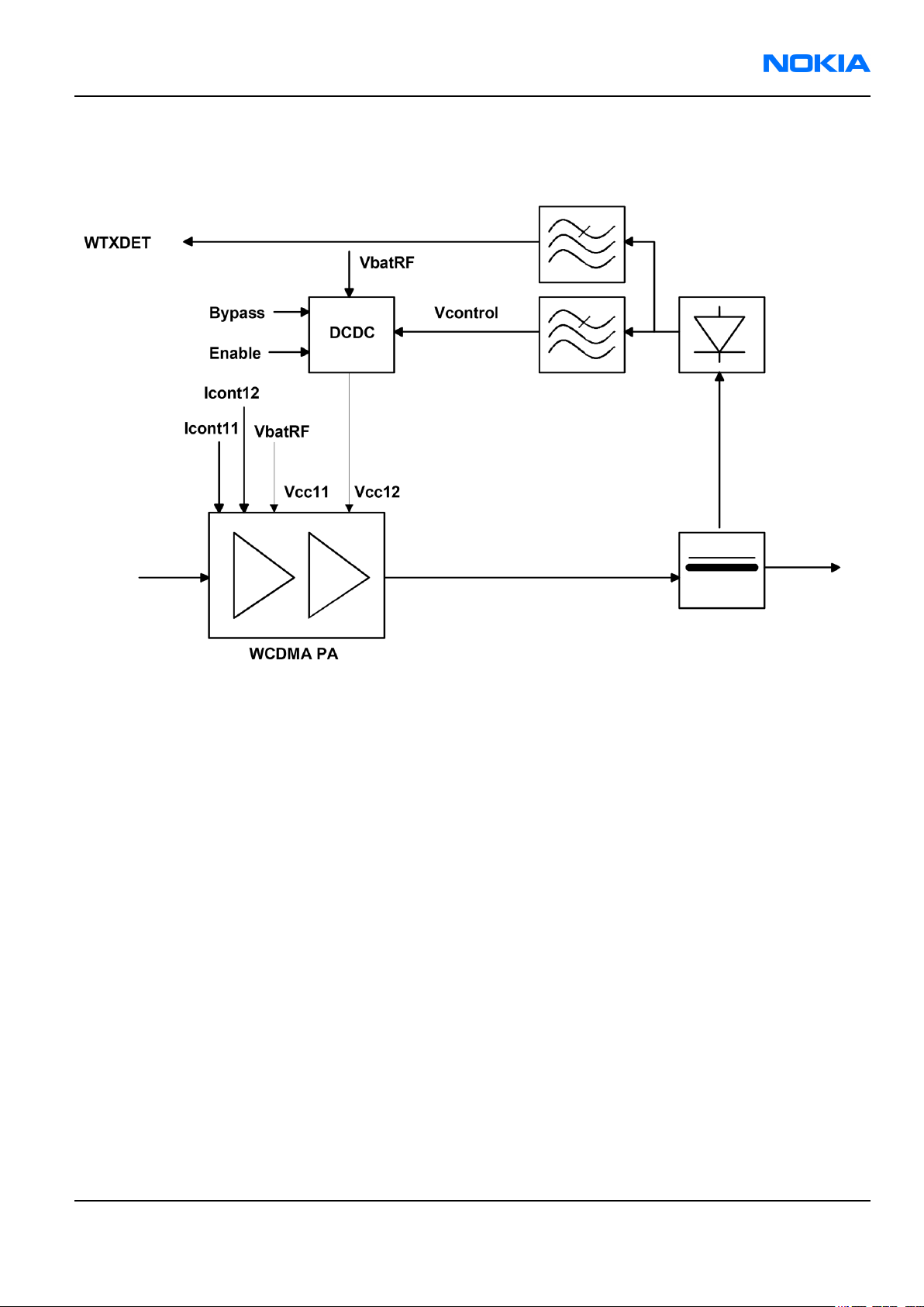
WCDMA PA module
WCDMA PA is housed in a separate module having
• a variable supply voltage input for the amplifier stages (Vcc11),
• a battery supply voltage for the bias circuits (Vcc12),
• and two bias current inputs.
Bias currents are generated by 5-bit DA converters in N7501 RF ASIC. The converters are controlled by BB via
RFBus.
In production the PA quiescent current is set according to PA vendor’s specifications. If another PA is changed
to the phone, this setting must be set again.
The bias currents are also used as PA on/off controls. The structure of the WCDMA PA is shown in the following
figure. The supply voltage for the output stage is got from a DCDC converter in order to improve the efficiency
at low power levels.
PA DCDC converter
The control of the DCDC converter is fed back from the power detector circuit.
Page 9–42 Company Confidential Issue 1
Copyright © 2004 Nokia. All Rights Reserved.
Page 43
RM-1
System Module Nokia Customer Care
The DCDC converter limits the lowest supply voltage to 1.5 V. At highest power levels the DCDC converter output
settles nominally to 3.2 V.
Figure 117 Block diagram of DCDC converter and WCDMA PA
GSM transmitter
An analogue IQ modulated signal is received to N7501 from digital BB.
The signal is first low pass filtered with filter corner frequency set to approximately 200 kHz. After the filter, the
signal is routed to the GSM modulator.
The appropriate routing after the modulator is selected by biasing either EGSM900 or GSM1800/1900 variable
gain amplifier. The amplifier gives 40 dB of power control dynamic range.
After the VGA stage the signal exits N7501. In case of GSM1800/1900 the signal goes directly to the GSM PA
module. In case of EGSM900, the PA module is preceded by a SAW filter. After the filter, the signal is fed to GSM
PA module. Finally the signal is routed via antenna switch to the antenna.
Issue 1 Company Confidential Page 9–43
Copyright © 2004 Nokia. All Rights Reserved.
Page 44

RM-1
Nokia Customer Care System Module
Figure 118 GSM transmitter
GSM power control
A closed control loop comprise an integrated power detector (in PA module) and an error amplifier. The error
amplifier resides in N7501, and it controls the transmitter power of GSM.
Detector output from the PA gives a DC level proportional to the output power. The DC voltage is fed to the
negative input of the error amplifier, where it is compared to the level of the reference signal, TXC. TXC is got
from the BB circuitry. The output of the error amplifier is fed to a buffer amplifier, which in turn steers the VGA
amplifier.
The TXC signal also contains the output power ramp waveform, which is optimized in order to meet the transient
spectrum and burst timing requirements. PA is switched on and off by changing the bias currents. As a result
the output power ramping and final power level of the transmitter are set in a controlled manner.
During EDGE operation 8-PSK modulation is utilized. In the 8-PSK modulation, there are envelope variations
during the data transmission. This presents extra requirement to the linearity of the PA. Therefore the PA is set
to a dedicated EDGE mode by setting a specific mode control signal up (Vmode). The bias currents are also
adjusted in order to improve the linearity.
Because of the 8-PSK modulation, the power control loop has to be opened during the data transmission in
EDGE mode. Otherwise a part of the envelope variations could be canceled out by control loop and signal
information contents and spectrum would be deteriorated. Loop is opened with a dedicated TXA-signal via
RFBus. When the power is ramped up, a modulating bit sequence producing a constant envelope waveform is
used and the power control loop is closed. Once the wanted power level has been reached, the loop is opened
and the power control voltage is kept constant by a capacitor integrated to N7501 Tx ASIC. When the active part
of the burst is over, the loop is again closed and the power is ramped down. The TXA signal is disabled during
GMSK transmission.
Power control loop is enabled and disabled by writing an appropriate register in N7501 RF ASIC. In case of dual
slot transmission, the output power is ramped down between the consecutive slots.
Page 9–44 Company Confidential Issue 1
Copyright © 2004 Nokia. All Rights Reserved.
Page 45

RM-1
System Module Nokia Customer Care
Figure 119 GSM/EDGE power control topology and control signals
Figure 120 Power control signal usage in GSM (GMSK) and EDGE (8PSK) transmission. Timings are not shown
accurately
Issue 1 Company Confidential Page 9–45
Copyright © 2004 Nokia. All Rights Reserved.
Page 46

RM-1
Nokia Customer Care System Module
GSM PA module
A single GSM/EDGE PA module contains two separate amplifier chains, one for EGSM900 and another for
GSM1800/1900. Both amplifiers have a battery supply connection and two bias current inputs. The bias current
for final amplifier stage is adjusted according the power level in use in order to optimise efficiency. The bias
currents are also used as on/off switching signals for PAs.
In the EDGE mode, PA linearity has to be higher than in GMSK mode because of envelope variations of the 8-PSK
modulations. This is achieved by increasing the bias currents compared to the GMSK mode and setting a
dedicated Vmode control signal up. Increasing bias currents improves the linearity of the amplifiers, but it also
tends to unnecessarily increase the gain of the PA. Vmode control aims to keep the gain of the amplifiers down.
The bias current needed for the maximum and the lowest output powers is specified by a PA manufacturer.
The current for the intermediate power levels is then linearly adjusted between these two values.
PA detection
It is possible to use PAs manufactured by different vendors. Because of this it is possible to set manufacturer
specific bias values for the PA. PA is detected by DSP SW in manufacturing phase. If PA is changed this detection
routine must be rerun before Tx calibrations. Components R7518, R7522, R7528 and R7534 are part of PA version
detection circuitry.
Frequency synthesizers
RF has separate synthesizers for Rx and Tx. Both synthesizers consist of:
• PLL
• loop filter
• VCO
• balun
The VCO frequencies are locked by PLLs into a reference oscillator, VCTCXO.
The PLLs are located in N7500 and N7501 respectively and controlled via RFBus. PLL charge pump charges or
discharges the integrator capacitor in the loop filter depending on the phase of the measured frequency
compared to the phase of the reference frequency. The integrator output voltage is connected to the control
input of the VCO.
The VCOs operate at the channel frequency multiplied by two in GSM1800/1900/WCDMA and by four in EGSM900.
The required frequency dividers required for modulators are integrated in N7501 and those for demodulators
in N7500. The dividers are controlled via RFBus.
Page 9–46 Company Confidential Issue 1
Copyright © 2004 Nokia. All Rights Reserved.
Page 47

RM-1
System Module Nokia Customer Care
Figure 121 Phase locked loop in N7500 and N7501 (PLL)
Reference oscillators
As a reference oscillator for the frequency synthesizers a 38.4MHz VCTCXO (voltage controlled temperature
compensated crystal oscillator) is used.
The output signal of the VCTCXO is directly connected to both N7500 and N7501 where it’s used as synthesizer
reference. N7500 also contains a balanced buffered output for supplying the clock signal to the digital BB ASIC
and a single ended buffer for Bluetooth.
The frequency of the reference oscillator is locked into the frequency of the base station with the help of an AFC
voltage, which is generated in BB by DSP and converted by dedicated DAC.
Regulators
N7500 and N7501 contain integrated regulators to supply regulated voltages for their internal circuitry and
other RF parts. Rx VCO supply is got via a switch from N7500 VR1 regulator. VCO can be switched on and off by
controlling the switch via RFBus.
Supply voltage for the VCTCXO is provided by a BB mixed mode ASIC. The same supply is used for reference clock
input buffers (in N7500 and N7501), output buffers (from N7500 to BB) and for the digital control blocks of both
RF ASICs. When the VCTCXO regulator is set active, the control blocks of the RF ASICs also wake up. After that the
integrated regulators can be controlled via RFBus.
Other supplies, like 4.7V supply for PLL charge pumps and bias reference (VREFRF01) are also provided by the
BB mixed mode ASIC.
Issue 1 Company Confidential Page 9–47
Copyright © 2004 Nokia. All Rights Reserved.
Page 48

RM-1
Nokia Customer Care System Module
Figure 122 RF supply connections from the BB mixed mode ASIC
Page 9–48 Company Confidential Issue 1
Copyright © 2004 Nokia. All Rights Reserved.
Page 49

RM-1
System Module Nokia Customer Care
Frequency mappings
EGSM900 frequencies
Issue 1 Company Confidential Page 9–49
Copyright © 2004 Nokia. All Rights Reserved.
Page 50

RM-1
Nokia Customer Care System Module
GSM1800 frequencies
Page 9–50 Company Confidential Issue 1
Copyright © 2004 Nokia. All Rights Reserved.
Page 51

RM-1
System Module Nokia Customer Care
GSM1900 frequencies
Issue 1 Company Confidential Page 9–51
Copyright © 2004 Nokia. All Rights Reserved.
Page 52

RM-1
Nokia Customer Care System Module
WCDMA Rx frequencies
Page 9–52 Company Confidential Issue 1
Copyright © 2004 Nokia. All Rights Reserved.
Page 53

RM-1
System Module Nokia Customer Care
WCDMA Tx frequencies
Issue 1 Company Confidential Page 9–53
Copyright © 2004 Nokia. All Rights Reserved.
Page 54

RM-1
Nokia Customer Care System Module
(This page left intentionally blank.)
Page 9–54 Company Confidential Issue 1
Copyright © 2004 Nokia. All Rights Reserved.
 Loading...