

Page 1

Nokia Customer Care
NHL-12 Series Transceivers
6 - Baseband Description &
Troubleshooting
Issue 3 05/2005 COMPANY CONFIDENTIAL
Copyright © 2005 Nokia. All Rights Reserved.
Page 2

NHL-12 Company Confidential
6 - Baseband Description & Troubleshooting Nokia Customer Care
[This page intentionally blank]
2 © 2005 Nokia Corporation. Issue 3 05/2005
Page 3

NHL-12
6 - Baseband Nokia Customer Care
Glossary of Terms............................................................................................... 5
Baseband Top-Level Description ......................................................................8
Baseband block diagram ................................................................................... 8
Environmental specifications ............................................................................. 9
Normal and extreme voltages ..........................................................................9
Humidity ...........................................................................................................9
Frequencies in baseband................................................................................... 9
Baseband Architecture..................................................................................... 11
CMT side.......................................................................................................... 11
CMT memories ..............................................................................................12
APE side.......................................................................................................... 13
APE memories ...............................................................................................13
Energy management........................................................................................ 14
Power supply modes ......................................................................................14
Battery BL-5C ................................................................................................16
Current gauge (Zocus) ...................................................................................17
RTC capacitor ................................................................................................17
Power distribution ..........................................................................................18
DC characteristics............................................................................................ 19
Regulators ......................................................................................................19
Voltage regulators in BB for RF....................................................................... 21
Charging .......................................................................................................... 22
Audio circuitry .................................................................................................. 22
Earpiece .........................................................................................................23
Internal microphone ....................................................................................... 23
Integrated hands-free .....................................................................................23
Audio accessory receive path ........................................................................23
Audio control signals ......................................................................................24
Acoustics.......................................................................................................... 24
Earpiece acoustics .........................................................................................24
IHF speaker acoustics ...................................................................................24
Microphone acoustics .................................................................................... 24
Vibra motor ....................................................................................................25
Audio modes.................................................................................................... 25
Hand portable ................................................................................................25
Integrated hands-free audio mode (IHF) ........................................................25
Accessory audio mode ................................................................................... 26
APE audio mode ............................................................................................26
Bluetooth audio mode ....................................................................................26
Baseband External and Internal Signals and Connections .......................... 27
CMT internal signals and connections............................................................. 27
CMT external signals and connections............................................................ 27
BB-RF Interface................................................................................................. 30
Issue 3 05/2005 COMPANY CONFIDENTIAL 1
Copyright © 2004 Nokia. All Rights Reserved.
Page 4

NHL-12
Nokia Customer Care 6 - Baseband
NHL-12 User Interface....................................................................................... 32
S60 - LCD interface ......................................................................................... 32
LCD & keypad illumination .............................................................................34
Current consumption ......................................................................................35
Maximum ratings ............................................................................................ 35
Camera interface ............................................................................................. 35
Keyboard.......................................................................................................... 36
Bluetooth.......................................................................................................... 36
SIM Interface...................................................................................................... 38
System Connector Interface ............................................................................ 40
Universal Serial Bus (USB).............................................................................. 41
Accessory Control Interface (ACI) ................................................................... 42
VOUT (Accessory Voltage Regulator) ...........................................................42
HookInt............................................................................................................. 43
Charging .......................................................................................................... 43
DC-plug ..........................................................................................................44
VCHAR pins of system connector ..................................................................44
Baseband Serial Interfaces ..............................................................................45
Internal serial interfaces between CMT and APE ............................................ 45
XBUS .............................................................................................................45
XABUS ...........................................................................................................45
External serial interfaces.................................................................................. 45
MMC interface ................................................................................................45
IrDA interface .................................................................................................45
USB interface .................................................................................................45
Baseband Test Points....................................................................................... 46
List and description.......................................................................................... 46
Test points on bottom-side............................................................................... 50
Test points on top-side..................................................................................... 51
Baseband Troubleshooting.............................................................................. 53
Top level flowchart........................................................................................... 54
“Contact Service” on display............................................................................ 55
Dead or jammed phone ................................................................................... 56
Flash faults....................................................................................................... 57
CMT flash faults ............................................................................................58
APE flash faults ..............................................................................................59
APE memory troubleshooting.......................................................................... 60
OMAP1510 flash (Seija) ................................................................................60
OMAP1510 SDRAM ......................................................................................66
Energy management troubleshooting.............................................................. 69
Device does not stay on .................................................................................69
General power checking ................................................................................ 69
2 COMPANY CONFIDENTIAL Issue 3 05/2005
Copyright © 2004 Nokia. All Rights Reserved.
Page 5

NHL-12
6 - Baseband Nokia Customer Care
APE power checking (SMPS) ........................................................................71
Energy management calibration .................................................................... 72
ADC-reading ..................................................................................................73
Backup battery ...............................................................................................74
Charging troubleshooting................................................................................. 75
APE reset......................................................................................................... 78
OMAP1510 (Helen).......................................................................................... 79
Clocks troubleshooting..................................................................................... 82
Clocks troubleshooting..................................................................................... 89
APE-CMT troubleshooting............................................................................... 96
APE-CMT interfaces ......................................................................................96
CMT serial interfaces troubleshooting ............................................................. 98
CBUS .............................................................................................................98
FBUS .............................................................................................................98
MBUS .............................................................................................................98
USB troubleshooting........................................................................................ 99
IrDa interface troubleshooting........................................................................ 102
SIM card error................................................................................................ 106
UI failure......................................................................................................... 107
Display blank ................................................................................................107
Display distorted ..........................................................................................111
Display backlight dim or no backlight ...........................................................112
Keyboard backlight ......................................................................................113
Keyboard malfunction .................................................................................. 115
Bluetooth troubleshooting.............................................................................. 117
Bluetooth settings for Phoenix .....................................................................117
Bluetooth troubleshooting flowchart ............................................................. 118
Multimedia card (MMC) troubleshooting........................................................ 119
Audio faults.................................................................................................... 124
HP earpiece failure .....................................................................................124
HP microphone failure .................................................................................125
External earpiece failure .............................................................................. 126
External microphone failure ......................................................................... 128
IHF speaker failure .......................................................................................129
Accessory detection troubleshooting ............................................................. 131
Camera module troubleshooting.................................................................... 133
Terms ...........................................................................................................133
Image taking conditions effect on image quality .......................................... 133
Camera hardware failure message .............................................................. 138
Image quality analysis.................................................................................... 142
Possible faults in image quality .................................................................... 142
Testing for dust ............................................................................................ 142
Testing for sharpness ..................................................................................143
Bit errors ......................................................................................................143
Issue 3 05/2005 COMPANY CONFIDENTIAL 3
Copyright © 2004 Nokia. All Rights Reserved.
Page 6

NHL-12
Nokia Customer Care 6 - Baseband
[This page intentionally blank]
4 COMPANY CONFIDENTIAL Issue 3 05/2005
Copyright © 2004 Nokia. All Rights Reserved.
Page 7

NHL-12
6 - Baseband Nokia Customer Care
1. Glossary of Terms
A/D Analog to Digital
ACI Accessory Interface
AFC Automatic Frequency Control
APE Application Program Engine
ASIC Application Specific Integrated Circuit
BSI Battery Size Indicator
BT Bluetooth
BTEMP Battery Temperature
CBUS Nokia Proprietary Serial Interface for MCU
CDMA Code Division Multiple Access
CMT Cellular Mobile Telephone
D/A Digital to Analogue
DAC Digital to Analogue Converter
DAI Digital Audio Interface
DBUS Nokia Proprietary Serial Interface for DSP
DC Direct Current
DCT Digital Core Technology
DMA Direct Memory Access
DSP Digital Signal Processor
EMC Electro Magnetic Compatibility
FBUS Nokia Proprietary Serial Interface
FM Frequency Modulation
FMEA Failure Mode and Effect Analysis
GSM G lobal System for Mobile Communications
Helen P rocessor from Texas Instruments (also called OMAP1510)
HF Hands Free
HFCM Hands Free Common Mode
HW Hardware electronics including Audio, Energy Management, UIHW and BB
I2C Inter-IC Control bus
Issue 3 05/2005 COMPANY CONFIDENTIAL 5
Copyright © 2005 Nokia. All Rights Reserved.
Page 8

NHL-12
Nokia Customer Care 6- Baseband
IC Integrated Circuit
IF Interface
IHF Integrated Hands Free
IMEI International Mobile Equipment Identity
IO, I/O Input Output
LCD Liquid Crystal Display
LDO Low Drop Out
LED Light Emitting Diode
LSB Least Significant Bit
LTPSi Low Temperature Poly Silicon
MBUS Nokia Proprietary Serial Interface
MCU Micro Controller Unit
MMC Multi Media Card
MMU Memory Management Unit
MPU Micro Processing Unit
MSB Most Significant Bit
NTC Negative Temperature Coefficient
PS Power Save signal
PURX Power Up Reset
PWB Printed Wiring Board
PWM Pulse Width Modulation
RF Radio Frequency
RTC Real Time Clock
SDRAM Synchronous Dynamic Random Access Memory
SIM Subscriber Identity Module
SMPS Switch Mode Power Supply
SW Software
TFT Thin Film Transistor
TI Texas Instruments
uBGA Micro Ball Grid Array package
UEM Univer sal En ergy Management
6 COMPANY CONFIDENTIAL Issue 3 05/2005
Copyright © 2005 Nokia. All Rights Reserved.
Page 9

NHL-12
6 - Baseband Nokia Customer Care
UI User Interface
UPP Universal Ph one Processor
USB Univer sal Serial Bus
VBAT Battery Volt age
VCTCXO Voltage Controlled
VGA Video Graphics Array
XBUS Proprietary Nokia serial communication bus
Issue 3 05/2005 COMPANY CONFIDENTIAL 7
Copyright © 2005 Nokia. All Rights Reserved.
Page 10
NHL-12
Nokia Customer Care 6- Baseband
2. Baseband Top-Level Description
NHL-12 is an imaging category (IP2.5) phone introducing a high-quality colour LCD, improved
camera and EDGE for Americas. NHL-12 operates on triple-band GSM (850/1800/1900) and
E-GPRS networks, and supports enhanced interfaces for connectivity with BT (Bluetooth) and
USB (Universal Serial Bus).
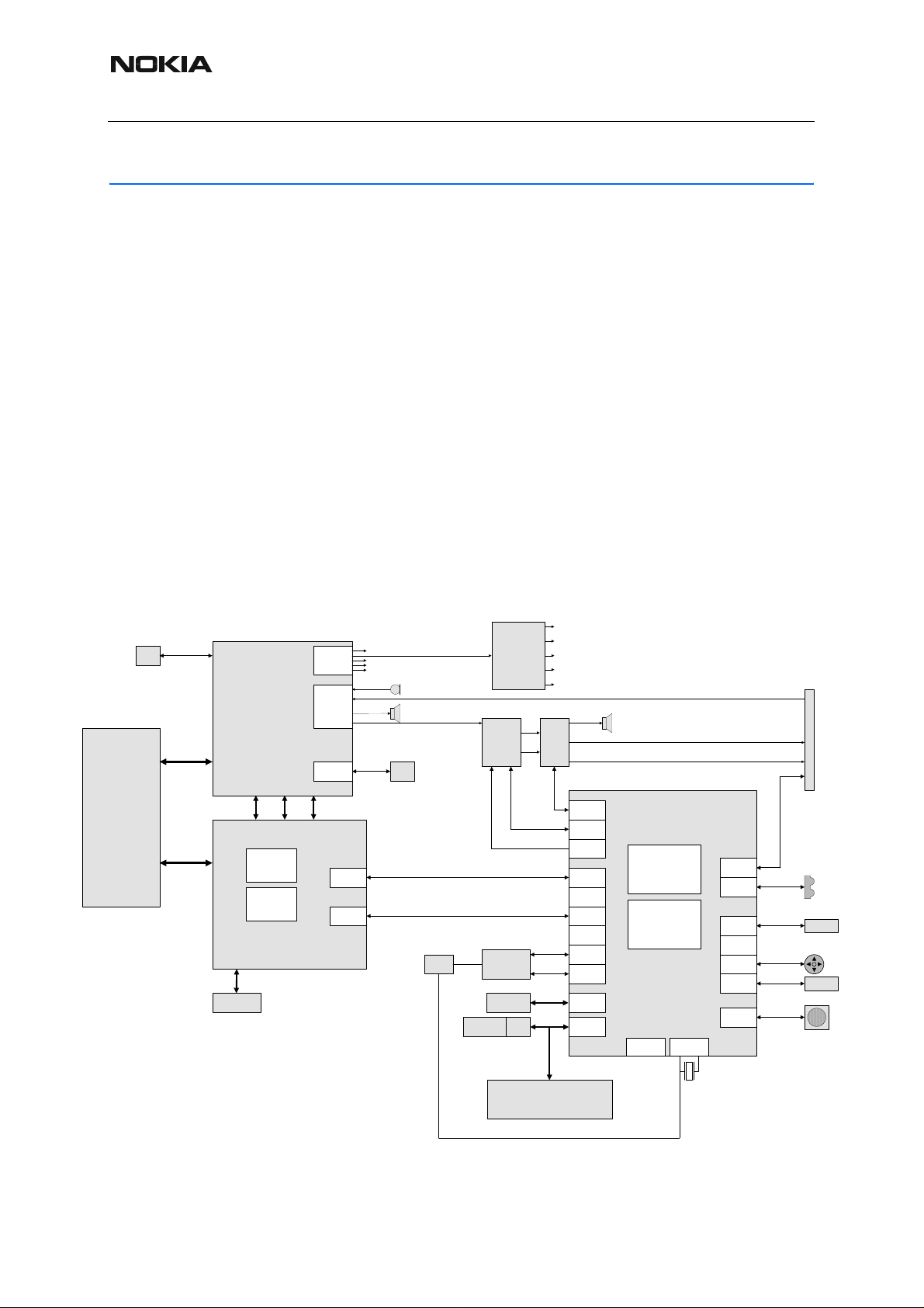
The NHL-12 baseband consists of a dual-processor engine and some product specific blocks,
such as IrDA and S60-display.
NHL-12 hardware and baseband consist of two parts: application part APE and phone part
CMT.
The APE part is constructed around an OMAP 1510 processor with SDRAM and NAND flash
memory as the core. Other major parts for APE are power, UI, audio, Bluetooth and camera.
APE and CMT parts are connected by serial communication buses and by a few control lines.
APE part reset and power control comes from the CMT side. Audio control is mostly performed
on the APE side, and phone audio is routed from the CMT side.
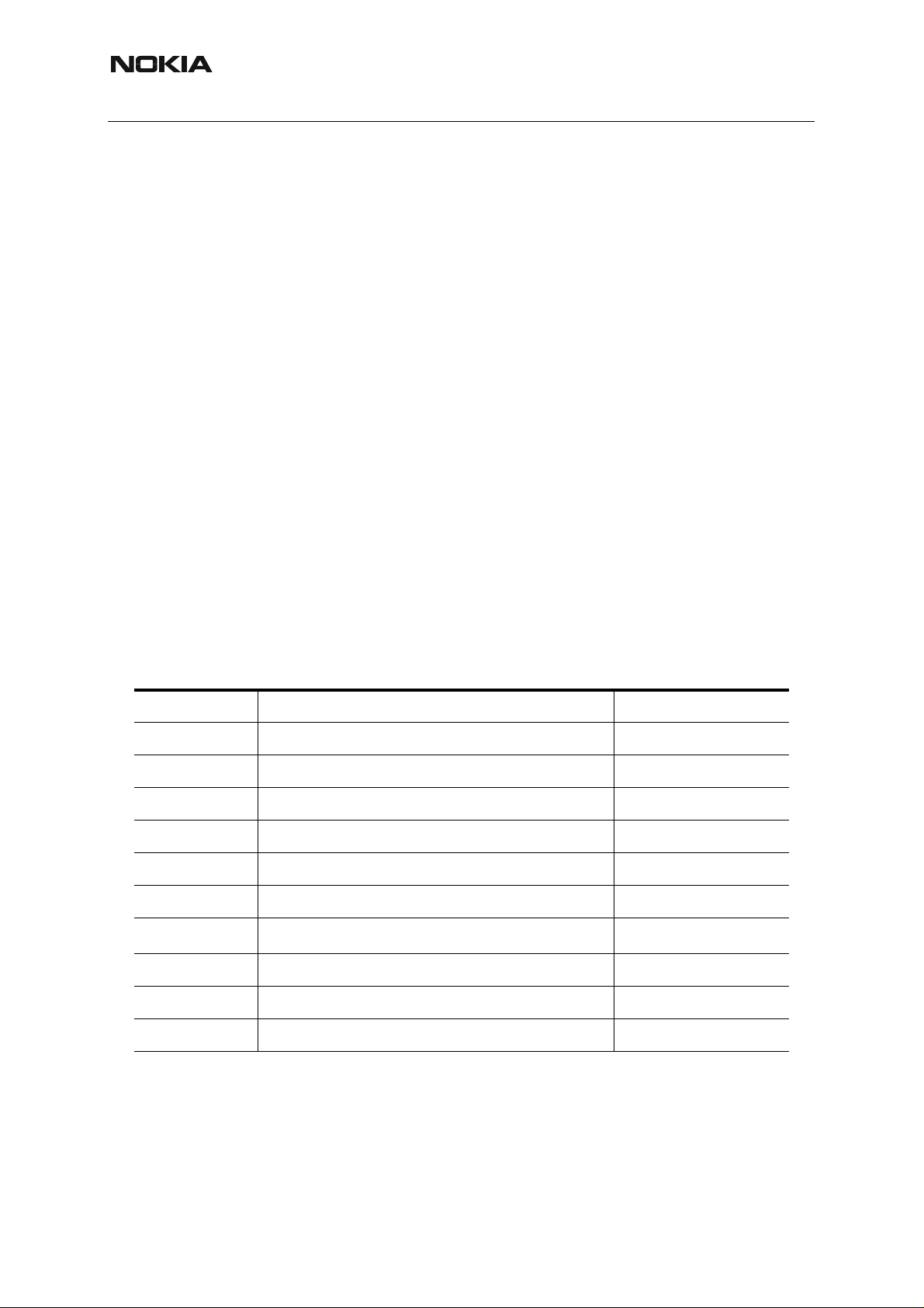
■ Baseband block diagram
The below system block shows the main BB function blocks.
Figure 1:Baseband block diagram
Flash
32Mb
ARM7
Lead3
UEM
UPP8M
BB
Regulators
CODEC
SIM I/F
LPRFUART
DSPSIO
Hands-free In
Hands-free Out
SIM
XBUS
XABUS
BT Clk
Buffer
Battery
RF
NAND 32MB
REGULATORS
DAC
Bluetooth
SDRAM 64MB
APE
Seija IF
Adapter
PA
McBSP2
I2C
McBSP1
UART2
GPIO I/F
MCSI2
McBSP3
UART1
MCSI1
SDRAM I/F
Flash I/F
OMAP1510
ARM925T
LEAD3ph3
LCD I/F CLKM
USB
UART3 /
PWT/PWL
SD-MMC
uWire
ARMIO
Keyboard
Camera
Bottom Connector
MIC
OUTL
OUTR
USB
IR
MMC
Rocker
Keyb
Display
12MHz
8 COMPANY CONFIDENTIAL Issue 3 05/2005
Copyright © 2005 Nokia. All Rights Reserved.
Page 11
NHL-12
6 - Baseband Nokia Customer Care
■ Environmental specifications
Normal and extreme voltages
• Nominal voltage:3.7V
• Lower extreme voltage:3.1V
• Higher extreme voltage:4.2V
Humidity
Operational humidity range is < 95%. Condensed or splashed water may cause interim or permanent phone malfunction.
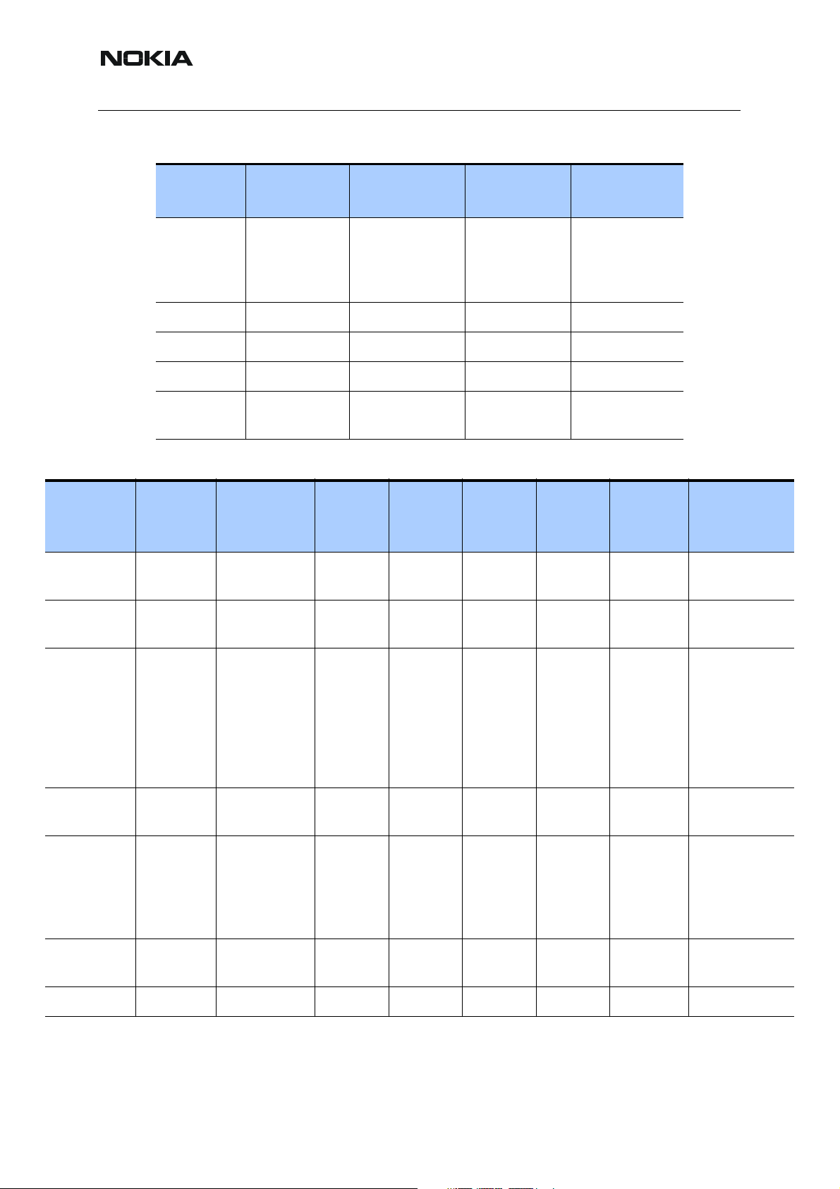
Table 1: Operational conditions
Environmental condition
Normal operation
Reduced performance
No operation
No operation or storage
Charging allowed
Long term storage condi-
tions
■ Frequencies in baseband
Ambient
temperature
-10 oC... +55 oC
+55 oC... +75 oC
o
C... -10 oC
-25
-40 oC... -20 oC
< -40 oC and > +85 oC
-25 oC... +60 oC
0 oC... +40 oC
Table 2: CMT clocks
Notes
Specifications fulfilled
Operational only for short periods
Operation not possible but an
attempt to operate will not damage the phone
No storage; an operation attempt
may cause permanent damage
Function Clock speed Location On/Off
VCTCXO 26 MHz VCTCXO/HELGO DSP/MCU is awake all the
time.
System Clock 13 MHz UPP DSP/MCU is awake all the
time.
DSP 195 MHz UPP DSP is awake all the time.
MCU 50.38 MHz UPP MCU is awake all the time.
Sleep clock 32.768 kHz UEM – UPP - OMAP During sleep mode
Issue 3 05/2005 COMPANY CONFIDENTIAL 9
Copyright © 2005 Nokia. All Rights Reserved.
Page 12
NHL-12
Nokia Customer Care 6- Baseband
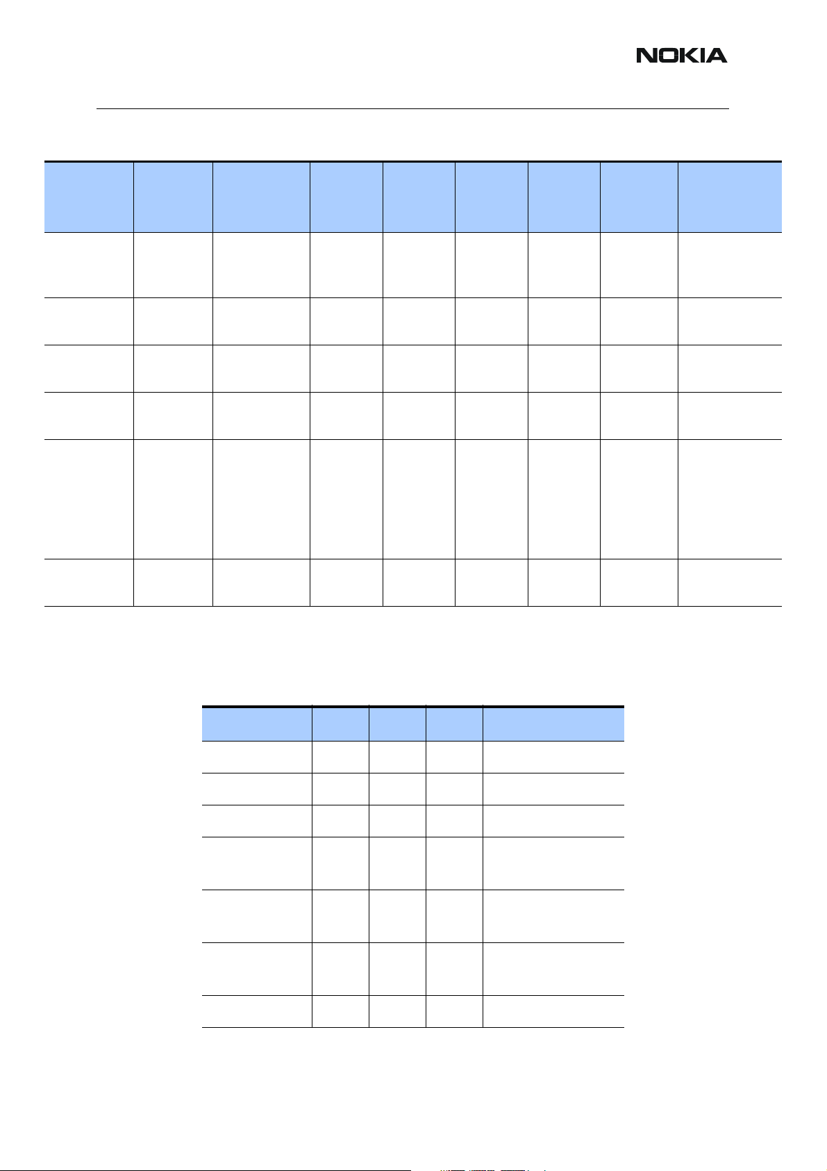
Table 2: CMT clocks
Function Clock speed Location On/Off
Cbus 1 MHz UPP–UEM/Zocus
Interface
Dbus 13 MHz UPP/UEM Interface During transceiver activity
RFConvClk 13 MHz UPP/UEM Interface During transceiver activity
RFBusClk 13 MHz UPP/HELGO Inter-
face
Flash 50.38 MHz UPP/Flash Interface Burst read accesses
SIM 3.25 MHz UPP/SIM Interface SIM accesses
Table 3: APE clocks
Function Clock Speed Source To Parameter
APE system clock 12 MHz Crystal OMAP1510 Frequency
OMAP DSP 150 MHz OMAP Internal DSP clock Frequency
OMAP MCU 150 MHz OMAP Internal MCU clock Frequency
CLK32K_IN 32768 Hz UEM OMAP1510
Generated continuously
whilst MCU is awake
During transceiver activity
Frequency
Sleep mode
Flash interface 37.5 MHz OMAP Flash – APE Frequency
SDCLK 75 MHz OMAP SDRAM – APE Frequency
BT 12 MHz Crystal BT module Frequency
MMC_CLK 16 MHz OMAP MMC Frequency
SCLK 12 MHz OMAP Audio DAC Frequency
Camera clock 12 MHz OMAP Camera Frequency
10 COMPANY CONFIDENTIAL Issue 3 05/2005
Copyright © 2005 Nokia. All Rights Reserved.
Page 13

NHL-12
6 - Baseband Nokia Customer Care
3. Baseband Architecture
■ CMT side
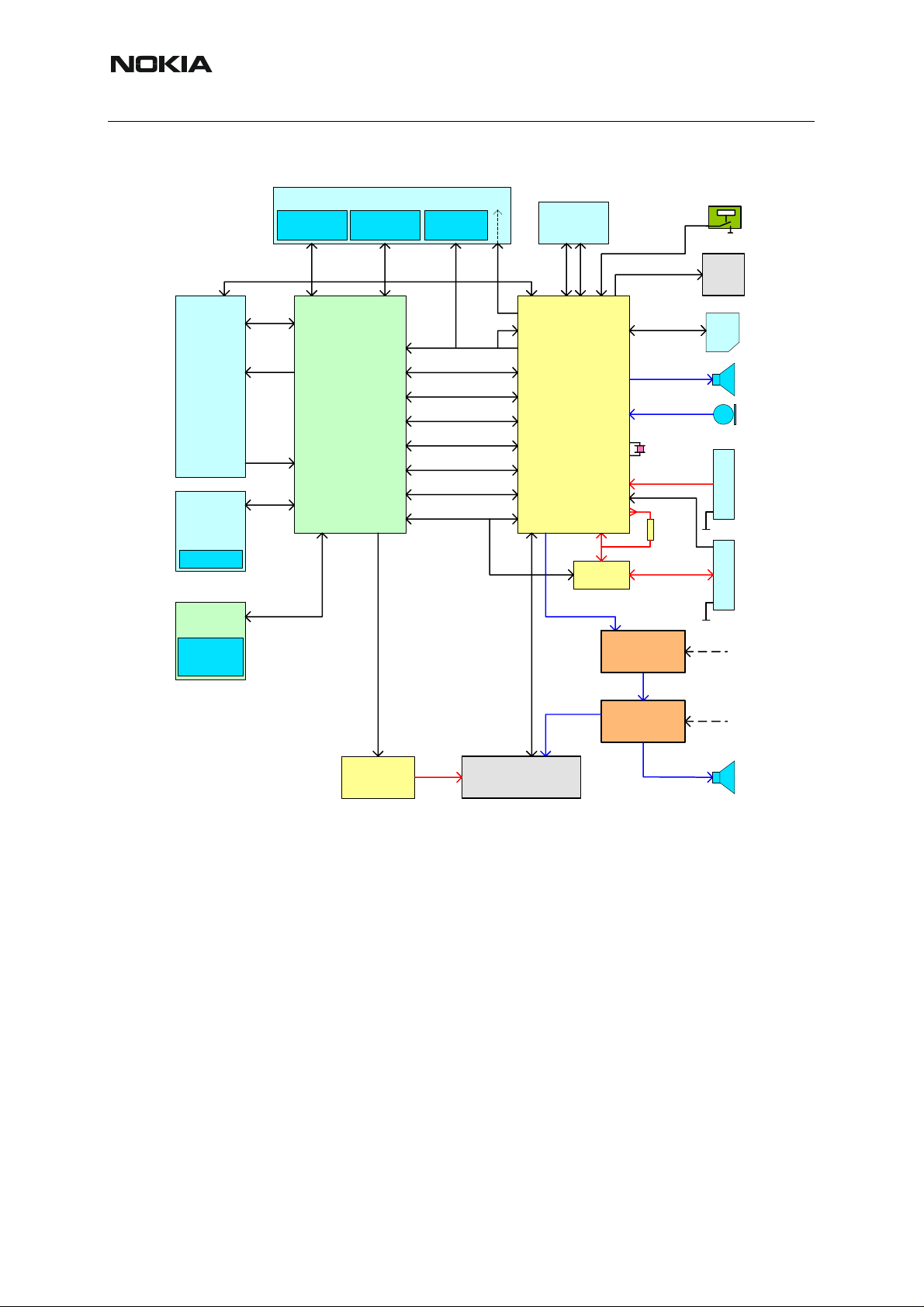
The CMT architecture is based on DCT4 Common Baseband.
The main functionality of the CMT baseband is implemented into two ASICs: UPP (Universal
Phone Processor) and UEM (Universal Energy Management).
System clock for the CMT is derived from the RF circuits. For the CDMA system, the RF clock
is 19.2 MHz and for GSM it is 26 MHz. The low frequency sleep clock is generated in the UEM
using an external 32.768kHz crystal. The I/O voltage of the CMT baseband is 1.8V. The analogue parts are powered from 2.8V power rails. The core voltage of UPP can be altered with
SW, depending on the prevailing processing power requirements.
UEM is a dual voltage circuit. The digital parts are running from the baseband supply (1.8V)
and the analogue parts are running from the analogue supply (2.8V). Some of th e UEM blocks
are also connected directly to the battery voltage (VBAT). UEM includes 6 linear LDO (low
drop-out) regulator for baseband and 7 regulators for RF. It also includes 4 current sources for
biasing purposes and internal usage. Some parts of the SIM interface have been integrated into
UEM. The SIM interface supports 1.8V and 3V SIM cards. Data transmission between the UEM
and UPP is handled via two serial buses: DBUS for DSP and CBUS for MCU. There are also
separate signals for PDM coded audio. Digital speech processing is handled by the DSP inside
UPP and the audio codec is in UEM.
The analogue interface between the baseband and the RF sections is implemented into UEM.
UEM provides A/D and D/A conversion of the in-phase and quadrature receive and transmit
signal paths and supplies the analogue TXC and AFC signals to the RF section under the UPP
DSP control. The digital RF-BB interface, consisting of a dedicated RFIC control bus and a
group of GenIO pins, is located in UPP.
The baseband supports both internal and external microphone inputs and speaker outputs. Input and output signal source selection and gain control is done in the UEM according to control
messages from the UPP. Keypad tones, DTMF and other audio tones are generated and encoded by the UPP and transmitted to UEM for decoding.
NHL-12 has two galvanic serial control interfaces for CMT: FBUS and MBUS.
Communication between the APE and CMT parts is handled through two serial buses: XBUS
and XABUS. XBUS is the main communication channel for general use, and XABUS is for audio data transfer. Also the system reset (PURX) and SleepClk for APE are coming from the
CMT side. The PURX is delayed approximately 130ms to fulfil OMAP1510 reset timing requirements and one of UEM’s IR level shifters is used for SleepClk level shifting.
Issue 3 05/2005 COMPANY CONFIDENTIAL 11
Copyright © 2005 Nokia. All Rights Reserved.
Page 14
NHL-12
Nokia Customer Care 6- Baseband
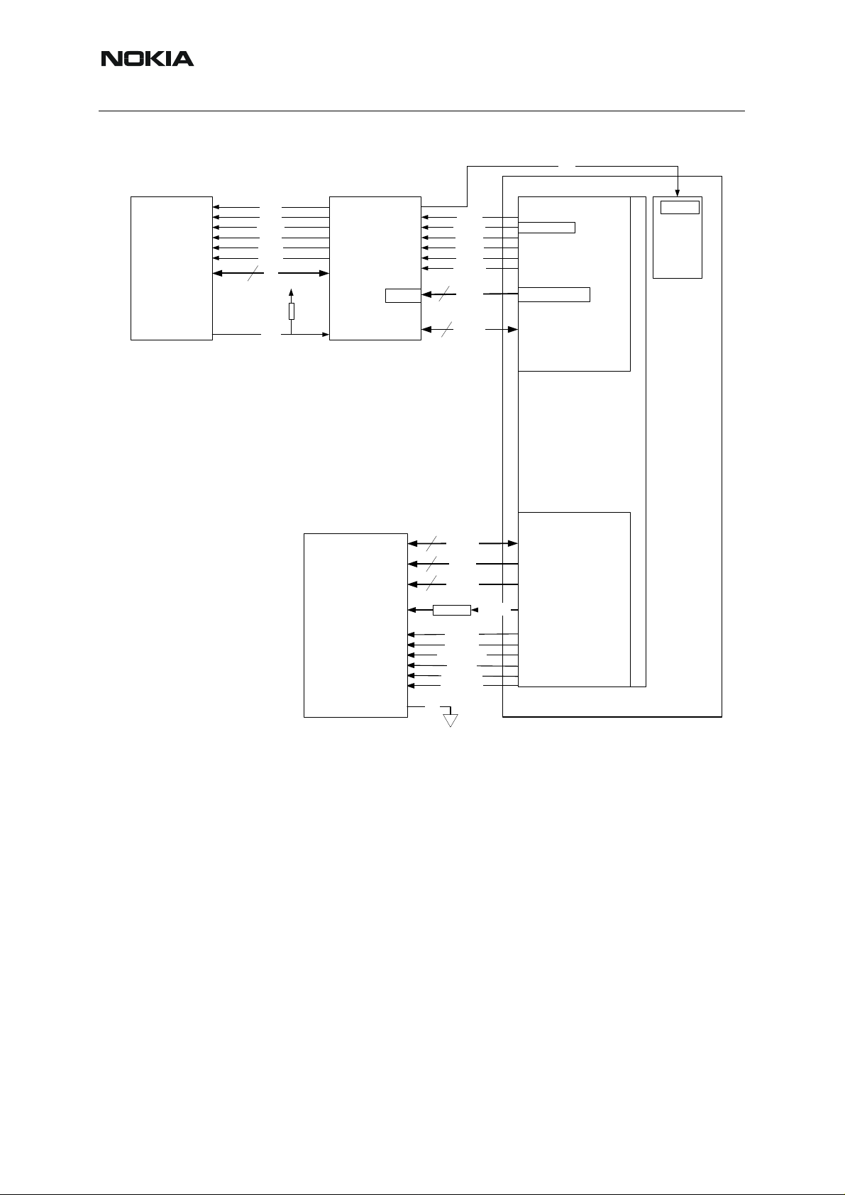
Figure 2:Simplified block diagram for CMT side
RF-BB
IF
R&D
Test IF
Ostrich
Memory
32Mb
Flash
RFConv
RFIC
Control
RF
Control
RFClk
CMT - APE interface
XBUS XABUS
UPP 8M
PWREn
130ms delay +
1V8 -> 2V8 LS
PURX
SleepClk
RFConvIF
Internal SIM IF
Audio IF
MBUS
FBUS
DBUS
CBUS
SleepClk
(2V8)
MIC+ACI
IRLEDC
IRTX
Prod/AS
Test IF
FBUS
MBUS
UEMK
UEM
Zocus
XEAR
L+R
Audio
Audio
DAC
DAC
Audio
AMP
32kH
L+R
z
CHRG
current
sense
PWR key
Vibra
SIM
EAR
MIC
BATT. IF CHRG. IF
Control
from APE
Accessory
regulator
System Connector
IHF
CMT memories
The memory interface supports 16-bit burst mode NOR FLASH with multiplexed add ress/data
bus, standard asynchronous 8-bit SRAM and 16-bit address/data multiplexed SRAM. The UPP
has two dedicated CS pins for FLASH and one GenIO that can be used as RAM CS.
The maximum amount of 16-bit SRAM with multiplexed address/data bus that can be connected to UPP is 2MBytes.
Memory configuration
The maximum amount of memory supported by UPP is 2*16MBytes of FLASH plus 2MBytes
of external SRAM.
CMT memory configuration includes 32Mbits of 54MHz NOR FLASH. The flash has readwhile-write capabilities.
12 COMPANY CONFIDENTIAL Issue 3 05/2005
Copyright © 2005 Nokia. All Rights Reserved.
Page 15

NHL-12
6 - Baseband Nokia Customer Care
■ APE side
The functionality of the APE engine is based on the OMAP1510 processor and memories. APE
has a total of 32 Mbytes of NAND type flash memory and 64 Mbytes of SDRAM.
The application engine has two separate clock sources: one for the system clock (12MHz) and
one for the sleep clock (32.768kHz), which is called Clk32k. The Clk32k is not generated by
the application engine, but is derived from the CMT SleepClk using a level shifter. The Clk32k
is always running when the engine is powered.
The 12MHz system clock is generated by OMAP1510. The crystal driver and related circuitry
is internal to the processor and an external quartz crystal is used as a frequency reference. The
Bluetooth clock is also derived from this clock using a clock buffer. Note that the system clock
is switched off during sleep mode.
The APE reset (MPU_nReset) is controlled by the CMT reset (PURX) generated by UEM.
PURX and MPU_nReset have different logic levels, but the latter is not simply a level shifted
version of the former. There is also an external delay circuit connected between the PURX and
MPU_nReset lines that keeps the APE reset active circa 130ms after CMT reset is released.
OMAP1510 consists of:
• DSP megamodule with internal program and data memory, instruction cache,
DMA controller and hardware accelerator
• ARM925T based processor megamodule with memory management unit (MMU),
instruction and data cache
• local bus with MMU
• multi-channel system DMA controller
• peripherals (local and shared) that support glueless system interface
• connecting modules that facilitate communication between these megamodules
and system memory (external and internal), and enhance system’s throughput and
software development.
OMAP 1510 is optimized for various multimedia and wireless applicat ions such as wireless video and image processing, wireless audio applications, graphics and video display acceleration.
APE memories
APE memory system consists of a 64Mbyte(32Mx16) SDRAM device connected to the
OMAP1510 fast external memory interface (EMIFF) and a 32Mbytes(32Mx8) of NAND-flash
device connected via Seija Flash-Interface Adapter ASIC to the OMAP1510 slow external
memory interface, EMIFS. The memory interface is shown in Figure 3, “APE external memories,” on page 14. NAND-flash is used as a boot the device and mass memory. User data is
stored in NAND. The operating voltage of all memory components is 1.8V, supplied from V18.
Issue 3 05/2005 COMPANY CONFIDENTIAL 13
Copyright © 2005 Nokia. All Rights Reserved.
Page 16
NHL-12
Nokia Customer Care 6- Baseband
Figure 3: APE external memories
INT
256Mb
NAND-flash
32Mx8
fCLE
fALE
fnCE1
fnRE
fnWE
fnWP
8
4.7kohm
fR/B
I/O
Seija Flash-
interface
adapter
512Mb
SDRAM
32Mx16
[11:0]
FCLK
NFCS0
NFOE
NFWE
NFRP
NFAVD
FADD
12
FDATA
16
SDATA
16
SADD
13
SBANK
2
22ohm SDCLK
NSCAS
NSRAS
SDCLK_EN
NSWE
NSDQML
NSDQMU
CS
NFCS0
EMIFS
[24:1]->[12:1]
EMIFF
Traffic Controller
OMAP1510
GPIO9
Interrupt
Handler
Memories are packaged as follows:
• SDRAM, 54ball CSP, 10x11.5x1.1mm, 0.8mm pitch Pb-free balls
• NAND, 63ball TBGA, 11x9x0.9mm, 0.8mm pitch Pb-free balls
• Seija ASIC, 64ball FBGA, 6x6x1.2mm, 0.5mm pitch Pb-free balls
■ Energy management
The energy management of NHL-12 is based on BB 4.0 architecture. BL-5C battery supplies
power primarily to the UEM ASIC and the RF PA. UEM includes several regulators to supply
RF and baseband. It provides the energy management including power up/down procedure.
Power supply modes
The state machine in UEM controls mainly the operating modes of the eng ine. State transitions
are enabled by signals taken from UEM, UPP and OMAP1510. In general, the state transitions
are based on the following information:
14 COMPANY CONFIDENTIAL Issue 3 05/2005
Copyright © 2005 Nokia. All Rights Reserved.
Page 17

NHL-12
6 - Baseband Nokia Customer Care
• Battery voltage (HW limits and cutoffs)
• Back-up battery voltage limits and cutoffs
• Power key status (in NHL-12 engine power key connected to PWRONX pin of
UEM)
• Delays generated by the state machines
• Real time clock (RTC) alarms
• Watchdogs
• Thermal shutdowns
• SLEEPX signal from UPP
• LOW_PWR signal from OMAP1510
The functional behaviour of the UEM can be divided into 6 different states. Since the UEM controls the regulated power distribution of the phone, each of these states affects the general
functionality of the phone:
• No supply
•Backup
• Power off
•Reset
• Power on
•Sleep
Brief description of operating modes
• NO_SUPPLY mode means that the main battery is not present or its voltage is
too low (below UEM master reset threshold limit) and back-up battery voltage is too
low.
• In BACK_UP mode the main battery is disconnected or empty but back-up battery
has sufficient charge in it
• IN POWER_OFF mode the main battery is present and its voltage is over UEM
master threshold limit. All regulators are disabled.
• RESET mode is a synonym for start-up sequence and contains in fact several
modes. In this mode certain regulators and system oscillators are enabled and after
they have stabilized, the system reset (PURX) is released and PWR ON mode entered.
• In POWER_ON mode SW is running and controlling the system.
• SLEEP mode is entered only from PWR ON mode when system activity is low.
CMT and APE sides can be in sleep mode independent of each other.
For controlling transitions between modes, UEM includes:
• RC oscillator (32kHz)
• crystal oscillator (32kHz)
• comparators
Issue 3 05/2005 COMPANY CONFIDENTIAL 15
Copyright © 2005 Nokia. All Rights Reserved.
Page 18
NHL-12
Nokia Customer Care 6- Baseband
• digital circuitry
These are used for generating limits and time delays.
Controlled powering off is done when the user requests it or when the battery voltage is fallin g
too low. Complete power down is done, if SW does not write to the watchdog register anymore
and a defined time after previous writing is elapsed. As this happen s, PURX is forced low and
all regulators are disabled. If the battery voltage falls below the very last SW–cutoff level, SW
will power off the system by letting the UEM’s watchdog elapse. If a thermal shutdown limit in
UEM regulator block is exceeded, the system is powered off. System reset PURX is forced low.
Uncontrolled powering off happens, when the battery is suddenly removed. This is problematic
as data may corrupt in memories, if the removal takes place during the access phase to these
devices. UEM’s state machine notices battery removal after battery voltage has been below
VCOFF– for 5 us and enters PWR_OFF mode. PURX is set low and all UEM’s regulators are
disabled.
There are three watchdogs in UEM. First one is for controlling system power-on and powerdown sequences. The initial time for this watchdog after reset is 32s. The time can be set using
a register. This watchdog is used for powering the system off in a controlled manner. The second one is for security block and is used during IMEI code setting. The third one is a power key
watchdog. It is used to power off the system in case SW is stuck and the user presses the power key. This watchdog, if not acknowledged by the SW, shuts down the system after a predefined delay (2–15 seconds). The feature is enabled as default and can be disabled by SW.
OMAP1510 also includes a hardware watchdog. This resets OMAP1510, BT and Seija at the
same time. It is possible to disable this watchdog with the help of SW.
Table 4: Reset thresholds and cutoff limits
VMSTR+ Master reset threshold 2.1 V
VMSTR– Master reset threshold 1.9 V
VCOFF+ Hardware cutoff 3.1 V
VCOFF– Hardware cutoff 2.8 V
VCHAR+ VCHAR detection threshold 2.0 V
VCHAR- VCHAR detection threshold 1.8 V
SW
CUTOFF
SW cutoff limit System dependent
VBUCOFF+ Backup battery cutoff 2.1 V
VBUCOFF– Backup battery cutoff 2.0 V
Battery BL-5C
The main battery of NHL-12 is a lithium ion battery BL-5C with the capacity of 850mA.
16 COMPANY CONFIDENTIAL Issue 3 05/2005
Copyright © 2005 Nokia. All Rights Reserved.
Page 19

NHL-12
6 - Baseband Nokia Customer Care
The battery interface has three pins: VBAT, GND and BSI. Temperature indication is located
on the engine PWB. Temperature measurement is performed using an NTC resistor (47k nom)
on the engine PWB.
Current gauge (Zocus)
The NHL-12 engine supports HW for phone and charging current measuring. The current
measurement chip that is used is LM3820. Current gauge is also supported by the ISA EM
Core SW. It can be used to estimate the battery charge level presented as batt ery bars on the
display.
Current is measured from the positive battery terminal using a sense resistor, so that all
phone’s consumed current flows through that resistor. Correspondingly, when charging, all current to phone’s battery flows through this resistor, but the direction is reversed. The sense resistor is formed from PWB tracks arranged as a 4-terminal resistor. LM3820 senses voltage
across the resistor. The maximum current depends on the sense resistor value.
RTC capacitor
Real Time Clock (RTC), crystal oscillator and backup battery circuitry are located inside the
UEM. Two regulators are used to provide needed voltages for external backup supply and
backup battery charging: VRTC for internal clock circuitry and VBU for backup battery charging.
The backup battery has voltage range VBACK = 2.0V
and discharged down to 2.0V).
min
– 3.2V
– 3.3V
typ
(charged to 3.2V
max
Charging the backup battery is controlled by the UEM’s digital block by enabling VBU regulator
and backup battery is charged with constant voltage up to 3.2V. By default, VBU regulator is
disabled in reset and it is reset always when PURX='0'.
Issue 3 05/2005 COMPANY CONFIDENTIAL 17
Copyright © 2005 Nokia. All Rights Reserved.
Page 20
NHL-12
Nokia Customer Care 6- Baseband
Power distribution
Figure 4: Power distribution diagram
Measurement resistor
TypeUnitOrDepartmentHere
LM3820
TypeYourNameHere TypeDateHere
UEM
VR1..7
VSIM
VANA
VFLASH1
VFLASH2
VCORE
VIO
BATTERY
7
RF
PA
Various
SIM
UPP
CORE
I/O
DOCUMENTTYPE 1 (1)
CMT FLASH
VCC
I/O
AUDIO PA
LP3985-2.8
2.8V
GENIO28 of UPP
LP3981-2.8
2.8V
LM2708-1.57
1.57V (SMPS)
LM2608-1.8
1.8V (SMPS)
LP3985-3.0
3.0V
GPIO15 of OMAP1510
Vout
V28
V15
V18
VMMC
Vbus
Klight (UEM) Uidrv(3)
Dlight (UEM) Uidrv(4)
System connector
Vout
USB cable
LP2985-3.3
3.3V
GPIO3 of OMAP1510
OMAP1510
I/O (2.8V) USB
I/O (1.8V)
CORE
TK11851L
(SMPS)
LM3350-4.1V
(SMPS)
V33
BT
CORE
I/O
AUDIO DAC
IR
NAND
FLASH+Seija
CORE+I/O
SDRAM
I/O
CORE
MMC
Display
Keyboard
Camera
Battery line
Power line
Control signal
Measurement signal
18 COMPANY CONFIDENTIAL Issue 3 05/2005
Copyright © 2005 Nokia. All Rights Reserved.
Page 21
NHL-12
6 - Baseband Nokia Customer Care
■ DC characteristics
Regulators
The transceiver baseband section has a multi-function analogue ASIC, UEM, which contains
six pieces of 2.78 V linear regulators and a 4.8 V switching regulator. All the regulators can be
controlled individually by the 2.78 V logic directly or through a control register.
The seven regulators are named VR1 to VR7. VrefRF01 and VrefRF02 are used as the reference voltages for Helgo, VrefRF01 (1.35V) for the bias reference and VrefRF02 (1.35V) for the
Rx ADC (analog-to-digital converter) reference.
The regulators (except VR7) are connected to Helgo. Different modes of operation can be selected inside Helgo according to the control information coming through the RFBus. UEM’s internal regulators are used for the powering of the baseband module. In addition to this, VIO and
VFLASH1 regulators of UEM are used to enable/disable APE side regulators.
VCORE and VSIM are programmable linear regulators. Default state for VCORE voltage is
1.57V.
There are also internal regulators in UEM. They are used for the powering of the CMT BB. In
addition to this, VIO and VFLASH1 regulators of UEM are used to enable/disable APE side regulators. BB4.0 supports only UEMKEdge or UEMC with UPP8Mv3.
NHL-12 APE energy management uses two switch mode power supplies: LM2608 and
LM2708, generating 1.57V and 1.8V to OMAP1510 and memories. In addition, the APE side
EM HW consists of several other discrete regulators:
• One linear regulator for 2.8V APE side logic (LP3981)
• One 2.8V linear regulator (LP3985) for powering the MMC card.
• One 3.3V linear regulator (LP2985) for powering the USB block of OMAP1510.
LM2608 is used to generate 1.8V for I/O’s OMAP1510 processor and APE side memories. Normally, LM2608 works in constant frequency PWM mode. But in the case of light loads, it is possible to control LM2608 via SYNC/MODE pin to low quiescent current mode. In this mode,
LM2608 works as a linear regulator and the output current capacity is only 3mA. LM2608 ne eds
an external 1.35V reference voltage. In the case of NHL-12 engine, this reference voltage is
taken from VrefRF01 of the UEM.
LM2708 is used to generate 1.57V for the core of OMAP1510 processor. LM2708 does not
need external reference voltage. Pin (Isel) can be used to adjust the current limit external coil.
NHL-12 engine has a higher current limit, which allows 400mA output current capacity.
In NHL-12 engine, LOW_PWR signal of OMAP1510 (multiplexed on pin ARMIO_5) is used to
control LM2708/LM2608 to linear mode when processor goes to deep sleep mode. The functionality of the LOW_PWR signal is the following: when OMAP1510 is in a low power state
(deep sleep mode), this signal is high. At reset and when in normal func tional mode, this signal
is low. Because the polarity SYNC/MODE pin is reverse, an additional inverter is used in this
control line.
Table 5: CMT regulators
Regulator
VIO 1.72 1.8 1.88 150
Issue 3 05/2005 COMPANY CONFIDENTIAL 19
Min VoltageVNom. VoltageVMax.VoltageVMax. Current
mA
Copyright © 2005 Nokia. All Rights Reserved.
Page 22
NHL-12
Nokia Customer Care 6- Baseband
Table 5: CMT regulators
Regulator
VCORE 1.053
VFLASH1 2.70 2.78 2.86 70
VFLASH2 2.70 2.78 2.86 40
VANA 2.70 2.78 2.86 80
VSIM 1.745
Regulator
Output
V15 SMPS
Type
mode
Min VoltageVNom. VoltageVMax.VoltageVMax. Current
200
1.35
1.57
1.8
2.91
Regulator
Type
LM2708-
1.57
1.8
3.0
Table 6: APE regulators
Main
Voltage
V
1.523 1.57 1.617 400 VFLASH1OMAP Core
Min
Voltage
V
1.855
3.09
Max
Voltage
V
25
Max
Current
mA
mA
Enabled byUsed for
Block
Linear
mode
V18 SMPS
mode
Linear
mode
V28 Linear LP3981-2.8 2.716 2.8 2.884 300 VIO OMAP I/O,
VMMC Linear LP2985ITL
V33 Linear LP2985-3.3 3.201 3.3 3.399 150 GPIO3 Helen USB
LM2608-
1.8
X-3.0
1.282 1.35 1.418 15
1.764 1.8 1.836 400 VIO OMAP I/O,
SDRAM
Core+I/O,
NAND
Flashes+
Seija, LCD,
camera
1.710 1.8 1.890 3
BT
Audio DAC,
LCD, camera, IR
2.91 3.0 3.09 150 GPIO15 MMC
20 COMPANY CONFIDENTIAL Issue 3 05/2005
Copyright © 2005 Nokia. All Rights Reserved.
Page 23
NHL-12
6 - Baseband Nokia Customer Care
Table 6: APE regulators
Regulator
Output
Type
Regulator
Type
Main
Voltage
V
Min
Voltage
V
Max
Voltage
V
Max
Current
mA
Enabled byUsed for
Block
USB host - 4.3 5.0 5.25 100 USB Regu-
lator Input
range
VOUT Linear LP3985-2.8 2.716 2.8 2.884 150 GENIO28Accessory
powering
V15 SMPS
mode
Linear
LM2708-
1.57
1.523 1.57 1.617 400 VFLASH1OMAP Core
1.282 1.35 1.418 15
mode
V18 SMPS
mode
LM2608-
1.8
1.764 1.8 1.836 400 VIO OMAP I/O,
SDRAM
Core+I/O,
NAND
Flashes+
Seija
VKEYB SMPS
mode
LM3353NOPB4.038 4.1 4.161 80mA UEM
Klight
Keypad leds
■ Voltage regulators in BB for RF
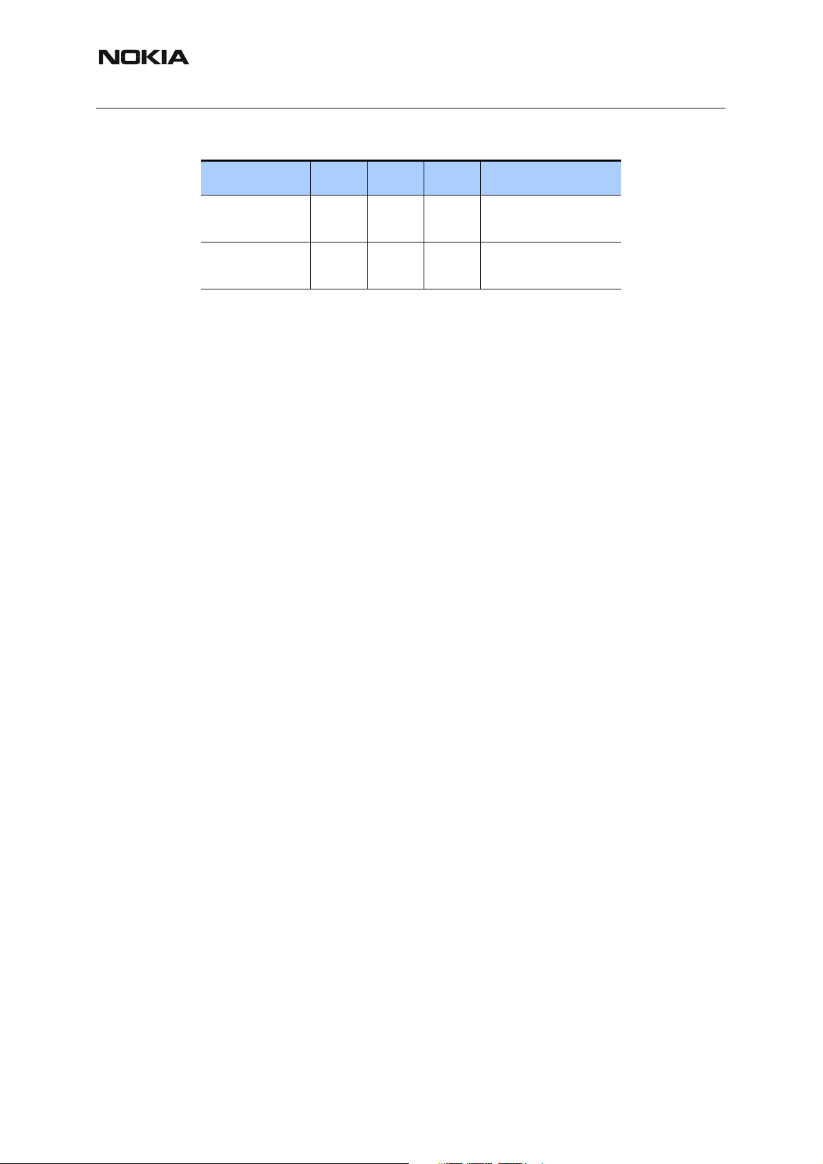
Values are referenced to GND unless otherwise specified.
Table 7: Voltage regulators in BB for RF
Signal Min Nom Max Note
VR1A / VR1B 4.6V 4.75V 4.9V I
VR2 2.70V 2.78V 2.86V I
VR3 2.70V 2.78V 2.86V I
VR4 2.70V 2.78V 2.86V I
VR5 2.70V 2.78V 2.86V I
VR6 2.70V 2.78V 2.86V I
VR7 2.70V 2.78V 2.86V I
= 10mA
max
= 100mA
max
= 20mA
max
= 50mA
max
I
sleep
= 50mA
max
I
sleep
= 50mA
max
I
sleep
= 45mA
max
= 0.1mA
= 0.1mA
= 0.1mA
Issue 3 05/2005 COMPANY CONFIDENTIAL 21
Copyright © 2005 Nokia. All Rights Reserved.
Page 24
NHL-12
Nokia Customer Care 6- Baseband
Table 7: Voltage regulators in BB for RF
Signal Min Nom Max Note
VrefRF01 1.334 1.35 1.366 Reference voltage
Imax = 0.1mA
VrefRF02 1.323 1.35 1.377 Reference voltage
Imax = 0.1mA
■ Charging
Charging control and charge switch are located in the UEM.
There is a thermal protection circuitry in the UEM to protect the chip. If temperature rises above
the threshold(150×C typ.), a charge switch is opened immediately and charging is stopped.
When the chip cools down, charging is continued normally.
HW supports all DCT4 chargers. 3-wire chargers are supported, but 3-wire charging is not. In
practice this means that the 3-wire chargers are internally connected (charger control wire connected to GND) as 2-wire chargers.
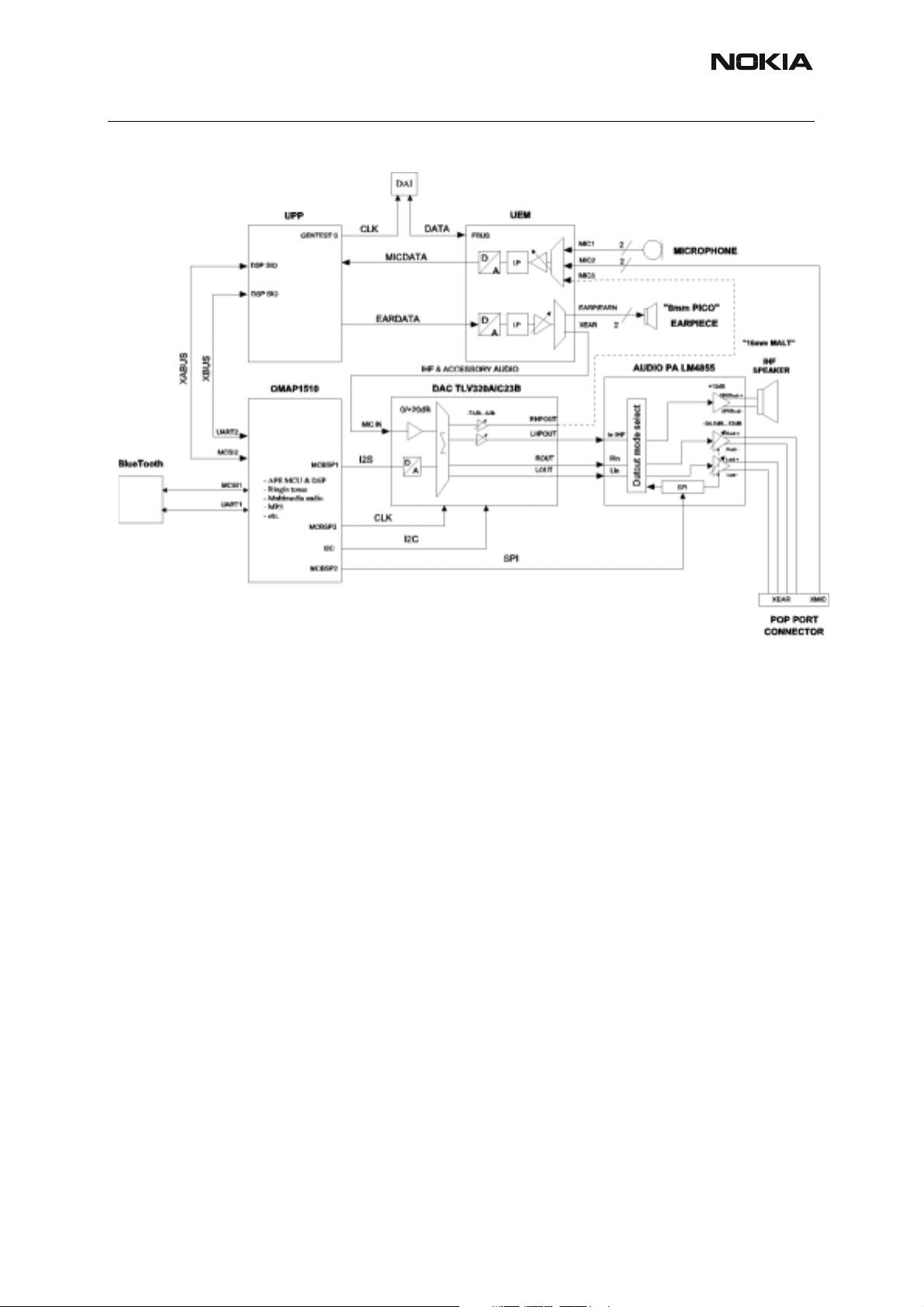
■ Audio circuitry
This section describes the audio HW of the engine. External audio components and acoustics
are not considered in detail in this section.
As this engine is based on dual-processor architecture, also audio is divided into separate APE
and CMT parts. Audio control is mostly on the APE side; phone audio is routed from the CMT
side to APE in analogue form, except Bluetooth which is in digital form. On the CMT side, audio
HW is integrated into the UEM ASIC. On the APE side, the most important parts are
OMAP1510, audio DAC and audio power amplifier.
The stereo output of this amplifier is designed for use with the ext ended Pop-port
It also has a differential mono output for driving the handsfree speaker.
The battery voltage (VBATT) is used directly as supply voltage for audio amp lifier. The nominal
battery voltage is 3.6V.
The type of DAC used is TLV320AIC23B and the supply voltage for this is coming from V28.
TM
connector.
22 COMPANY CONFIDENTIAL Issue 3 05/2005
Copyright © 2005 Nokia. All Rights Reserved.
Page 25
NHL-12
6 - Baseband Nokia Customer Care
Figure 5:NHL-12 audio block diagram
Earpiece
NHL-12 uses an earpiece which is a 32 ohm speaker with a diameter of 8 mm. The supply voltage is 2.7V. The earpiece is driven differentially directly by the UEM. The ca psule is mou nted
into the LCD frame assembly.
Internal microphone
The internal microphone is mounted in the B-cover. The microphone is omnidirectional and it
is connected to the UEM microphone input MIC1P/N. The microphon e input is asymmetric and
the UEM (MICB1) provides the bias voltage. Nominal impedance of the microphone is
1.8kOhms. The microphone input to UEM is ESD protected. Spring contacts are used to connect the microphone to the main PWB.
Integrated hands-free
Integrated hands-free speaker (IHF), 16mm, is used to generate alertin g and warning tones in
NHL-12. The IHF speaker is driven with audio amplifier. The speaker capsule is mounted in the
antenna module. Spring contacts are used to connect the IHF speaker contacts to the main
PWB.
Audio accessory receive path
In NHL-12 the accessory receive path is directly driven from the UEM HF / HFCM differential
audio outputs. The output signal complies with the Pop-port accessory interface.
For EMC protection, ferrites are connected in series to the earpiece and for ESD protection bizener is used.
Issue 3 05/2005 COMPANY CONFIDENTIAL 23
Copyright © 2005 Nokia. All Rights Reserved.
Page 26
NHL-12
Nokia Customer Care 6- Baseband
Audio control signals
The HEADINT signal is needed for recognizing the external device (e.g. headset) connected
to the system. The recognition is based on the ACI-pin on the system connector.
The button of the external device generates HOOKINT. This is used, for example, to answer or
to end a phone call.
■ Acoustics
Earpiece acoustics
The earpiece is a PSS 8mm element. The earpiece is placed inside the plastic UI frame. It is
sealed to UI support frame with a foam ring. This cavity is ported to a second cavity formed
between the UI support frame and A-cover with Bezel. Sound holes vent this cavity out of the
UI support flame. All holes are shielded to prevent dust and small particles from entering the
phone.
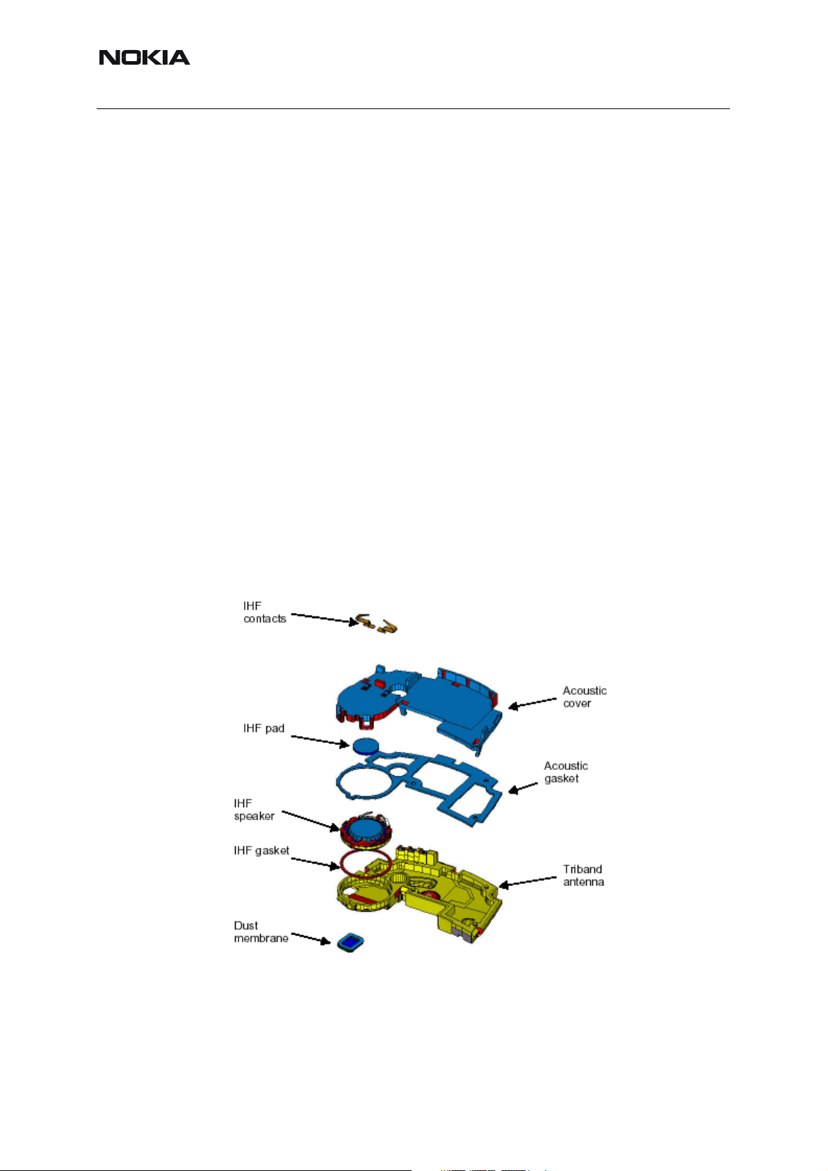
IHF speaker acoustics
In NHL-12, the IHF speaker is used for integrated hands-free and ringing tone applications. It
has a structure, which consists of two cavities: one back cavity and one front cavity.
When using the phone in the IHF mode, speech is fed to the IHF-speaker. Ringing tones are
optimized according to bandwidth and frequency response. The sound holes are placed in the
B-cover. Sound holes are shielded to prevent dust and small particles from entering the phone.
Figure 6:Exploded view of antenna assembly.
Microphone acoustics
NHL-12 has a standard microphone module. The module is embedded into a so-called "rubber
boot" and connected to the system module by spring contacts.
24 COMPANY CONFIDENTIAL Issue 3 05/2005
Copyright © 2005 Nokia. All Rights Reserved.
Page 27

NHL-12
6 - Baseband Nokia Customer Care
The microphone is placed close to the system connector. The sound port of the microphone is
located towards the bottom of the phone.
Vibra motor
A vibra alerting device is used to generate a vibration signal for an incoming call. It is located
in the middle part of the phone and it is connect ed to the main PWB with spring contacts. The
vibra is controlled by a PWM signal coming from UEM. The vibra motor is mounted in the Bcover assembly.
■ Audio modes
This section describes NHL-12’s engine audio modes. The following audio modes are supported:
• Hand portable
• Integrated hands-free
• Accessory audio mode
• APE audio mode
• Bluetooth audio mode
Hand portable
Hand portable mode is the basic audio mode. This is entered when no audio accessories are
connected and the hands-free mode is not selected.
In the hand portable mode, earpiece path and internal microphone path are in use.
A call is created by the CMT. The uplink signal is generated by the microphone and transferred
to MIC1P/N differential inputs. The internal microphone is enabled using the MICB1 bias voltage O/P on UEM. The signal is amplified at least by 20 dB, low pass filtered, converted into
digital domain and then postponed through UPP to transducer equalizer and finally to APE for
speech encoding.
The EAR output on the UEM is selected for Rx audio via the internal earpiece. The UEM sets
the audio uplink gain and downlink attenuation. Different downlink attenuation levels function
as the volume control.
The internal earpiece is driven by the CMT engine for voice calls. The internal microphone is
driven by the CMT for voice calls and voice recording.
All volume controls are handled by the UEM.
Integrated hands-free audio mode (IHF)
This mode is entered by user selection.
A call is created by the CMT. The uplink signal is generated by the microphone and transferred
to MIC1P/N differential inputs. The internal microphone is enabled using the MICB1 bias voltage O/P on the UEM.
The downlink audio is processed in the UPP and transferred to the UEM. Then the downlink
signal is amplified in the single-ended XEAR Output driver in the UEM. The mono XEAR output
is connected to the MICIN input of the APE Audio DAC via a low-pass filter. The signal is then
routed through the line output of DAC (LHPOUT), high pass filtered and routed to the
Phone_In_IHF input. This drives the internal speaker via the SPKRout driver.
Issue 3 05/2005 COMPANY CONFIDENTIAL 25
Copyright © 2005 Nokia. All Rights Reserved.
Page 28

NHL-12
Nokia Customer Care 6- Baseband
Accessory audio mode
This mode is entered when an audio accessory (mono/ stereo headset, loopset, basic ca r kit)
is connected to the system connector. The routing of the audio signal is identical for all accessories (except for the stereo headset), but gain control depends on the accessory used.
The call is created by the CMT. The uplink signal is generated by the external microphone and
transferred to the UEM MIC2 input, after which the MIC2B bias voltage and MIC2P/N inputs
are enabled on the UEM.
The downlink audio signal is routed through the single-ended XEAR output driver by the UEM.
The mono XEAR output is connected to the MICIN input of the DAC via a lo pes filter. Then signal is routed through L
Accessories are driven via the system connector using the L
stereo headset is used also the R
OUT
and R
drivers of DAC to the L
OUT
driver is connected. Both channels play the same mono
OUT
and RIN inputs of the LM4855.
IN
driver of LM4855. When a
OUT
audio signal.
APE audio mode
This mode is entered when a user starts a multimedia application (e.g. MP3, AAC etc.) or in
the case of ringing tones/ other notification tones played via the IHF speaker or the system connector.
When an MP3 is played, encoded data is read from the MMC card and the decoding is performed by OMAP1510. After decoding, the raw linear data is sent to the external audio DAC as
a 16-bit PCM audio through the I2S connection. The DAC performs the digital-to-analogue-audio conversion.
For playback and streaming of digital audio, synthesized ring tones, miscellaneous tones, and
game sounds, the APE side can be selected to drive either the IHF speaker or the system connector.
For playback via the internal speaker, the LHPOUT output on the audio DAC is used. The signal is routed to Phone_in_IHF input on LM4855.
For playback via the stereo/ mono headset or other accessories, the L
of the Audio DAC are used. These are routed to the L
/RIN inputs of the LM4855. In the case
IN
OUT
and R
OUT
outputs
of mono accessory, OMAP1510 produces a monophonic signal to DAC.
Bluetooth audio mode
Bluetooth audio data is transferred using a separate interface, MCSI.
MCSI is a serial (voice) interface with multi-channels transmission capability. There are two in-
dependent MCSI interfaces in OMAP1510 and one of them, MCSI1, is connected to the PCM
interface of BC02. The MCSI1 is a half-duplex interface and it can work as either master or
slave. This 4-wire interface has a bi-directional serial clock and frame synchronization. MCSI
has a programmable word length (from 3 to 16 bits) and frame configuration.
26 COMPANY CONFIDENTIAL Issue 3 05/2005
Copyright © 2005 Nokia. All Rights Reserved.
Page 29
NHL-12
6 - Baseband Nokia Customer Care
4. Baseband External and Internal Signals and Connections
This section describes some of the external and internal electrical connections and interface
levels on both CMT and APE side. The electrical interface specifications are collected into tables that cover a connector or a defined interface.
■ CMT internal signals and connections
Table 8: Internal microphone
Signal Min Nom Max Condition Note
MICP 200mV
AC 2.2kΩ to MIC1B
pp
2.0 V 2.1 V 2.25 V DC
MICN 2.0V 2.1V 2.25V DC
Table 9: Internal speaker
Signal Min Nom Max Condition Note
EARP
0.75V 0.8V
EARN
0.75V 0.8V
2.0 V
0.85V
2.0 V
0.85V
pp
pp
AC
DC
AC
DC
Differential output
= 4.0 Vpp)
(V
diff
■ CMT external signals and connections
Table 10: DC connector
Pin Signal Min Nom Max Condition Note
1 VCHAR 11.1V
7.0 V
RMS
8.4 V
peak
RMS
16.9 V
7.9 V
1.0 A
9.2 V
850 mA
peak
RMS
peak
RMS
Standard charger Charger positive
input
Fast charger
2 CHGND 0 Charger ground
Issue 3 05/2005 COMPANY CONFIDENTIAL 27
Copyright © 2005 Nokia. All Rights Reserved.
Page 30
NHL-12
Nokia Customer Care 6- Baseband
TM
U/I
levels
connector
Impedance Notes
Pin Signal Description
Table 11: Pop-port
Spectral
range
1 CHARGE V Charge DC 0-9 V /
0.85 A
2 GND Charge GND 0.85 A 100 mΩ (PWB + conn.)
3 ACI ACI 1 kbit/s Dig 0 /
2.78V
4 VOUT DC out DC 2.78V /
47 Ω Insertion & removal
detection
100 mΩ (PWB + conn.) 200mW
70mA
5 USB VBUS DC in DC 4.375-
Connected to APE side
5.25V
6 USB D+ 12M 0-3.3V Connected to APE side
7 USB D- 12M 0-3.3V Connected to APE side
8 USB Data
GND
Data GND Ferrite to
engine GND
9 XMIC N Audio in 300 - 8k 1Vpp &
DC
2.78V
10 XMIC P Audio in 300 - 8k 1Vpp &
DC
2.78V
11 HSEAR N Audio out 20 - 20k 1Vpp 10 Ω
12 HSEAR P Audio out 20 - 20k 1Vpp 10 Ω
13 HSEAR R NAudio out 20 - 20k 1Vpp 10 Ω Not conn. In mono
14 HSEAR R PAudio out 20 - 20k 1Vpp 10 Ω Not conn. In mono
Table 12: Electrical characteristics of SIM connector
Pin Name Parameter Min Typ Max Unit Notes
1 VSIM 1.8V SIM Card 1.62 1.8 1.98 V Supply voltage
3V SIM Card 2.7 3.0 3.3 V
2 SIMRST 1.8V SIM Card 0.8xVSIM
0
VSIM
0.2xV
V SIM reset (output)
SIM
3V SIM Card 0.8xVSIM
0
VSIM
0.2xV
V
SIM
28 COMPANY CONFIDENTIAL Issue 3 05/2005
Copyright © 2005 Nokia. All Rights Reserved.
Page 31

NHL-12
6 - Baseband Nokia Customer Care
Table 12: Electrical characteristics of SIM connector
Pin Name Parameter Min Typ Max Unit Notes
3 SIMCLK Frequency 3.25 MHz SIM clock
T
rise/Tfall
max 50 ns
T
rise/Tfal
1.8V V
1.8V V
3V V
oh
3V V
ol
4 DATA 1.8V V
1.8V V
3V V
oh
3V V
ol
1.8V V
1.8V V
3V V
il
3V V
il
l 50 ns
oh
ol
0.7xVSIM
0
VSIM
0.2xV
SIM
0.7xVSIM
-0.3
VSIM
0.2xV
SIM
oh
ol
ih
il
0.7xVSIM
-0.3
0.7xVSIM
-0.3
0.7xVSIM
-0.3
VSIM
0.3
VSIM
0.3
VSIM
+0.3
0.2xV
SIM
0.7xVSIM
-0.3
VSIM
+0.3
0.2xV
SIM
V
V
V SIM data (output)
V SIM data (input)
T
rise/Tfall
max 1µs
5 NC Not connected
6 GND GND 0 0 V Ground
Issue 3 05/2005 COMPANY CONFIDENTIAL 29
Copyright © 2005 Nokia. All Rights Reserved.
Page 32

NHL-12
Nokia Customer Care 6- Baseband
5. BB-RF Interface
The interface between the baseband and the RF section is mainly handled by the UEM ASIC.
UEM provides A/D and D/A conversion of the in-phase and quadrature receive and transmit
signal paths and also A/D and D/A conversions of the received and transmitted audio signals
to and from the user interface.
The UEM supplies the analogue TXC and AFC signals to the RF section according to the UPP
DSP digital control. Data transmission between the UEM and the UPP is implemented using
two serial busses: DBUS for DSP and CBUS for MCU. There are also separate signals for PDM
coded audio. Digital speech processing is handled by the DSP inside UPP ASIC. UEM is a dual
voltage circuit: the digital parts are running from the baseband supply 1.8V and the analogue
parts are running from the analogue supply 2.78V; also VBAT is directly used.
The table below describes all the analogue signals from the baseband block to the RF block
and back. The signal names are based on the schematics.
Table 13: Analogue signals between BB and RF
Signal
Name
VCTCXO VCTCXO UPP Frequency 26 MHz High stability
From To Parameter Min Typ Max Unit Function
clock signal for
the logic circuits,
AC coupled. Distorted sinewave
e.g. sawtooth.
Signal amplitude
BB load
resistance
BB load
capacitance
DC level 1.3 1.35 1.4 V
Input imped-
ance
DC level 1.17 1.20 1.23 V
0.2 1.32 Vpp
10 kohm
10 pF
500 kohm
Source
impedance
TXQP /
TXQN
30 COMPANY CONFIDENTIAL Issue 3 05/2005
UEM Helgo Same spec
as for TXIP /
TXIN
Copyright © 2005 Nokia. All Rights Reserved.
200 ohm
Page 33

NHL-12
6 - Baseband Nokia Customer Care
Table 13: Analogue signals between BB and RF
Signal
Name
AFC UEM VCTCXO Voltage Min
TXC UEM Helgo Voltage Min
RFTemp Helgo UEM Voltage at -
From To Parameter Min Typ Max Unit Function
Max
Source
impedance
Max
Source
impedance
Load
resistance
capacitance
20 deg.C
0.0
2.4
200 ohm
2.4
5
1,57 V Temperature
0.1
2.55
0.1 V Transmitter
200 ohm
15
V Automatic fre-
kohm
pF
quency control
svoltage for the
VCTCXO
power level and
ramping control
sensor of the RF.
Voltage at
+25 deg.C
Voltage at
+60 deg.C
DC_sensePA UEM Voltage 0.7 1.35 2.0 V PA final stage
IPA1&IPA2UEM PA Output volt-
age
Current
range
Resolution 4 bit s
0 2.7 V PA final stage
0 5 mA
1,7
1,79
quiescent current level information
quiescent current adjustment
Issue 3 05/2005 COMPANY CONFIDENTIAL 31
Copyright © 2005 Nokia. All Rights Reserved.
Page 34

NHL-12
Nokia Customer Care 6- Baseband
6. NHL-12 User Interface
The row and column lines of the UI are controlled by OMAP1510 and backlights by UEM.
Figure 7, “BB UI connections,” describes the BB user interface connections:
Figure 7:BB UI connections
Keyboard
LCD
Display
IR Link
Earpiece
IHF
speaker
Baseband
Microphone
Vibra
Pop-Port
System Connector
■ S60 - LCD interface
The user interface features a 176x208 pixel active matrix colour TFT display with 65536 colours.
The backlight voltage is generated using a regulator (D4451). Figure 8, “Interface connections.,” shows the LCD interface connections:
32 COMPANY CONFIDENTIAL Issue 3 05/2005
Copyright © 2005 Nokia. All Rights Reserved.
Page 35

NHL-12
6 - Baseband Nokia Customer Care
Figure 8:Interface connections.
OMAP1510
!FLASH.OE
!FLASH.CS1
FLASH.AD(2)
!FLASH_WR
FLASH.D(7:0)
ARMIO2
V28
100k
8
Level shifter
100R
RC1
470p
PURX
100p
RC2
220R
LCD module
E
M
I
+
E
S
D
F
I
L
T
E
R
!RD
!CS
D_!C
!WR
D(7:0)
!RESET
TE
The interface uses a 8-bit data transfer. Partial display function is implemented in the module.
Issue 3 05/2005 COMPANY CONFIDENTIAL 33
Copyright © 2005 Nokia. All Rights Reserved.
Page 36

NHL-12
Nokia Customer Care 6- Baseband
LCD & keypad illumination
In NHL-12, white LEDs are used for LCD lighting and blue for keypad lighting. There are four
blue LEDs for keypad backlight. All LEDs have their own series resistors. A step-up DC-DC
converter is used as a LED driver.
Table 14: DC characteristics and PIN assignments
Pin no. Symbol i/O Description
1 GND Ground
2
3
4
5 D1 Bi-directional Data bus
6 D2 Bi-directional Data bus
7 D3 Bi-directional Data bus
8 GND Ground
9
10
11
12 LEDin Power supply LED anode
13 LEDout Power supply LED cathode
14 L_GND Ground Guard ring ground for LEDs
15 ICS Input Chip select (low active)
16
17
18
IWR
GND
D0
VDDI
VDD
LGND
DAC
GND
D7
Input
Ground
Bi-directional
Power supply
Power supply
Ground
Input
Ground
Bi-directional
Memory write enable (low active
Data bus
Supply voltage for digital circuits
Supply voltage for analogue circuits
Guard ring ground for LEDs
Data/command information signal
Data bus
19 D6 Bi-directional Data bus
20 D5 Bi-directional Data bus
21 D4 Bi-directional Data bus
22 TF Output Tearing effect
23
24
34 COMPANY CONFIDENTIAL Issue 3 05/2005
IRD
IRES
Input
Input
Copyright © 2005 Nokia. All Rights Reserved.
Memory read enable (low active)
Reset signal (low active)
Page 37

NHL-12
6 - Baseband Nokia Customer Care
Current consumption
Table 15: LCD interface current consumption
Maximum ratings
Table 16: LCD interface absolute maximum ratings
■ Camera interface
NHL-12 features a built-in VGA camera.
The camera control interface operates by I2C bus.
The camera module itself is assembled into the metal frame and connected to the PWB via a
20-pin spring connector.
Camera powering voltages, V28&V18, are routed through the X4450 connector.
Issue 3 05/2005 COMPANY CONFIDENTIAL 35
Copyright © 2005 Nokia. All Rights Reserved.
Page 38

NHL-12
Nokia Customer Care 6- Baseband
■ Keyboard
The keyboard interface of OMAP1510 is a 6x5 matrix interface. The keyboard interface pins
are normal IOs with 30/70 decision limits at 2,8 operating voltage: 1.96V high level an d 0,84V
low level.
Table 17: Key connection example
Kbr(0) Kbr(1) Kbr(2) Kbr(3) Kbr(4) Kbr(5)
Kbc(0) Soft1 Soft2
Kbc(1) App/Averell
Kbc(2) Edit 1 4 7
Kbc(3) * 2 5 8
Kbc(4) # 3 6 9
Kbc(5) Clear 0 Send End
Table 18: Rocker connection
ARMIO0
ARMIO7 ARMIO4 ARMIO1
ARMIO6
■ Bluetooth
Bluetooth provides a fully digital link for communication between master unit and one or more
slave units. The system provides a radio link that offers a high degree of flexibility to support
various applications. Data and control interface for a low power RF module is provided. Data
is regulated between the master and the slave.
The Bluetooth system in NHL-12 is compliant with the Bluetooth specification V1 .1. The system
is based on single chip Bluetooth solution, BC02. The chip contains radio and baseband parts
as well as MCU and on-chip ROM memory. Together with some external components (matching components, filter, balun etc.) and an antenna, it forms the Bluetooth system, which can be
attached to the host (OMAP1510). Bluetooth components are mounted directly to the PWB.
36 COMPANY CONFIDENTIAL Issue 3 05/2005
Copyright © 2005 Nokia. All Rights Reserved.
Page 39

NHL-12
6 - Baseband Nokia Customer Care
Figure 9:Bluetooth system
Issue 3 05/2005 COMPANY CONFIDENTIAL 37
Copyright © 2005 Nokia. All Rights Reserved.
Page 40

NHL-12
Nokia Customer Care 6- Baseband
7. SIM Interface
UEM contains the SIM interface logic level shifting. SIM interface supports 3V and 1.8V SIMs.
SIM supply voltage is selected by a register in the UEM. It is only allowed to change the SIM
supply voltage when the SIM IF is powered down.
The SIM interface is powered up when the SIMCardDet signal indicates "card in". This signal
is derived from the BSI signal.
Table 19: SIM interface signals
Parameter Variable Min. Typ Max Unit
SIMCARDet, BSI comparator Threshold Vkey 1.94 2.1 2.26 V
SIMCARDet, BSI comparator Hysteresis (1) Vsimhyst 50 75 100 mV
The entire SIM interface is located in two chips: UPP and UEM.
The SIM interface in the UEM contains:
• power up/down
• port gating
• card detect
• data receiving
• ATR-counter
• registers
• level shifting buffers logic
The SIM interface is the electrical interface between the SIM card and the mobile phone (via
UEM device).
38 COMPANY CONFIDENTIAL Issue 3 05/2005
Copyright © 2005 Nokia. All Rights Reserved.
Page 41

NHL-12
k
k
6 - Baseband Nokia Customer Care
Figure 10:SIM interface NHL-12
SIM
C5 C6 C7
C1
C3
C2
C8
C4
From
SIM
ASIP
SIMIO
SIMCl
SIMRst
VSIM
BSI
UEM
SIMIF
register
SIMIO
SIMCl
SIMRst
UEM
digital
logic
UPP
SIMIO
SIMClk
SIMR
UEMInt
CBusDa
CBusEnX
CBusClk
UIF Block
Issue 3 05/2005 COMPANY CONFIDENTIAL 39
Copyright © 2005 Nokia. All Rights Reserved.
Page 42

NHL-12
Nokia Customer Care 6- Baseband
8. System Connector Interface
The system connector in NHL-12 is a Pop-Port
TM
connector. It consists of a charging plug
socket and system connector. The Pop-Port is a feature-based interface. The accessory contains information about its features (ACI ASIC) and it is detected with a fully digital detection
procedure.
TM
Four new functions are introduced with the Pop-Port
system connector interface:
• Accessory control interface (ACI)
• Power out
• Stereo audio output
• Universal serial bus (USB)
Table 20: Pop-port
TM
functions
Function Note
Charging Pads for 2-wire charging in cradles
Audio 4-wire fully differential stereo audio output
Power supply for
2.78V/70mA output to accessories
accessories
ACI (Accessory Con-
Accessory detection/removal & controlling
trol Interface)
FBUS Standard FBUS, Fast FBUS
Note! NHL-12 does not support accessories using
FBUS serial interface.
USB (default) USB v.2.0 device mode (full speed 12M)
40 COMPANY CONFIDENTIAL Issue 3 05/2005
Copyright © 2005 Nokia. All Rights Reserved.
Page 43

NHL-12
P
P
P
6 - Baseband Nokia Customer Care
Figure 11:Pop-PortTM connections
PWB
Charge
Shielding GND
Charge GND
Table 21: Pop-port
ACI
Vout
USB D-
USB D+
USB VBUS
TM
connections
DATA GND
XMIC N
XMIC
HSEAR N
HSEAR
HSEAR R N
Pin # Signal Note
1 VCHAR
2 GND Charge ground
3 ACI Insertion & removal detection /Serial data
bi-directional 1 kbit/s
4 Vout 200mW
5 USB VBUS
6 USB D+/FBUS Rx
7 USB D-/FBUS Tx
8 USB data GND Data ground
HSEAR R
Shielding GND
9 XMIC N Negative audio in signal
10 XMIC P Positive audio in signal
11 HSEAR N Negative audio out signal.
Max bandwidth from the phone
12 HSEAR P Positive audio out signal.
Max bandwidth from the phone
13 HSEAR R N Not connected or grounded in mono.
14 HSEAR R P Not connected or grounded in mono.
■ Universal Serial Bus (USB)
The USB interface of OMAP1510 supports the implementation of a full speed device, fully compliant to USB2.0 standard. NHL-12 uses an integrated USB transceiver.
Issue 3 05/2005 COMPANY CONFIDENTIAL 41
Copyright © 2005 Nokia. All Rights Reserved.
Page 44

NHL-12
Nokia Customer Care 6- Baseband
OMAP1510 can provide a maximum of three sets of USB ports. One set is an integrated USB
transceiver and the other two sets are LVCMOS I/O pins that implement interfaces to external
transceivers. However, only the first set is available by default and used in the NHL-12 engine.
■ Accessory Control Interface (ACI)
ACI (Accessory Control Interface) is a point-to-point, bi-directional serial bus. ACI has two main
features: 1) detecting the insertion and/or removal of an accessory device and 2) acting as a
data bus.
Third feature provided by ACI is to identify and authenticate a specific accessory which is connected to the system connector interface.
All accessories cause headint interrupt when connected to or disconnected from the system
connector. The insertion of an accessory generates a headint interrupt by pulling the ACI line
down. When no accessory is present, the UEM’s internal headint pull-up resistor keeps the line
.
high
All accessories have a common detection start sequence, when phone gets headint interrupt
from high to low transition in the ACI pin.
Figure 12:Principle schematics of ACI accessory and engine
VOUT (Accessory Voltage Regulator)
An external LDO Regulator is needed for accessory power supply purposes. All ACI accessories require this power supply. Regulator input is connected to the battery voltage VBAT and
output is connected to the Vout pin. The regulator is controlled via UPP (On/Off-function).
42 COMPANY CONFIDENTIAL Issue 3 05/2005
Copyright © 2005 Nokia. All Rights Reserved.
Page 45

NHL-12
6 - Baseband Nokia Customer Care
Figure 13:Accessory power supply diagram
Table 22: Accessory power supplies
Signal Min Nom Max Note
Vout 2.70V 2.78 2.86V I
GenIO(28) 1.4 1.8 1.88
0.6
= 150mA
max
High (ON)
Low (OFF)
■ HookInt
The hookInt signal is generated by creating a short circuit between the headset microphone
signals. An LP filter is needed on the hookInt input to filter the audio signal. In this mode, the
earpiece signal on the HF and HFCM pins is in the opposite phase. The earpiece is driven differentially.
When no accessory is present, the hookInt signal is pulled up with the UEM resistor. When the
accessory is inserted and the microphone path is biased, the hookInt signal decreases to 1.8V
due to the microphone bias current flowing through the resistor. When the microphone button
is pressed, the microphone signals are connected together, and the hookInt input will get half
of micbias dc value 1.1 V. This change in DC level causes the hookInt comparator output to
change state, in this case from 0 to 1. The button can be used for answering incoming calls but
not to initiate outgoing calls.
Table 23: HookInt signals
Signal Min Nom Max Unit
VFLASH1 2.7 2.78 2.86 V
MICB2 2.0 2.1 2.25
600VuA
Vhook1 1.25 1.35 1.45 V
■ Charging
NHL-12 can be charged via a DC-plug or charging pins on the system connector. Only 2-wire
charging is supported.
Issue 3 05/2005 COMPANY CONFIDENTIAL 43
Copyright © 2005 Nokia. All Rights Reserved.
Page 46

NHL-12
Nokia Customer Care 6- Baseband
DC-plug
NHL-12 uses a 3.5mm DC-plug. 3-wire chargers are supported, but 3-wire charging is not. In
practice this means that the 3-wire chargers are internally connected (charger control wire connected to GND) as 2-wire chargers. 1Hz PWM signal is used to control UEM's charge switch.
VCHAR pins of system connector
The VCHAR and ChargeGND pin are directly connected to the normal charger lines of the DCplug.
Table 24: VCHAR pins of system connector
Signal Min Nom Max Unit Note
Input voltage range
(fast charger)
Input voltage range
(standard charger)
5.5 8.4 9.3 VRMS I= 850mA
11.1
7.9
-0.3 20 V Absolute maximum VHAR volt-
16 Vpeak
VRMS
age
44 COMPANY CONFIDENTIAL Issue 3 05/2005
Copyright © 2005 Nokia. All Rights Reserved.
Page 47

NHL-12
6 - Baseband Nokia Customer Care
9. Baseband Serial Interfaces
■ Internal serial interfaces between CMT and APE
XBUS
XBUS is the main communication interface between the CMT and APE engines. This 6-pin interface is a combination of a general 4-pin UART based interface and two wake-up signals.
XBUS has no test points and the signals are routed in the inner layers of the PWB.
XABUS
XABUS is a synchronous serial interface used for uncompressed PCM audio data transfer between the DSPs of UPP (CMT) and OMAP1510 (APE).
■ External serial interfaces
MMC interface
The MMC interface consists of a control block in OMAP1510, MMC regulator and EMC protection ASIP (R5200). MMC interface is a serial bus with three wires: data, command and clock
run at 16MHz. The regulator (N5200) output is VMMC.
IrDA interface
NHL-12 uses a TDFU5103 IR-module (V4451). It is compatible with 1.152Mbit IrDA 1.3.
Speeds up to 115kbits/sec are supported. Operating voltages are VBAT and V28.
USB interface
Pop-Port
compliant access. The interface consists of a USB regulator (N2001) supplying V33 to
OMAP1510 USB control block, and USB ASIP (R2003) for EMC protection.
TM
system connector has pins for USB interface, for a USB 2.0 full speed (12Mb/s)
Issue 3 05/2005 COMPANY CONFIDENTIAL 45
Copyright © 2005 Nokia. All Rights Reserved.
Page 48

NHL-12
Nokia Customer Care 6- Baseband
10. Baseband Test Points
■ List and description
Table 25: Baseband test points
Test point Signal Function Characteristics Note
J2400 MCSI2_DIN XABUS
receive data
J2401 MCSI2_DOUT XABUS trans-
mit data
J2402 MCSI2_SYNC XABUS syn-
chronization
J2404 COM_MCLK_REQXABUS clock
request
J2405 MCSI2_CLK XABUS clock 12 MHz digital
N4800#3 PURX Power_up
reset
J2801 SLEEPX Sleep mode
control signal
J2802 SLEEPClk Sleep mode
timing clock
1.8V digital signal Data to OMAP1510
1.8V digital signal Data from
8 kHz digital clock
1.8V
1.8V digital signal Clock request to
clock 1.8V
1.8V digital signal From UEM to UPP
1.8V when not in
sleep mode
0 V when in sleep
mode
32.768kHz digital
clock 1.8V
from UPP
OMAP1510 to UPP
Sync clock from
UPP to OMAP1510
OMAP1510 from
UPP
Clock from
OMAP1510
From UPP to UEM
From UEM to UPP;
J2803 UEMINT Interrupt
request from
UPP
J4815 CLK32k sleep mode
clock
J2807 MB USTX MBUS from
UPP to UEM
J2808 MBUSRX MBUS from
UEM to UPP
J2809 FBUSTX FBUS from
UPP to UEM
J2810 FBUSRX FBUS from
UEM to UPP
46 COMPANY CONFIDENTIAL Issue 3 05/2005
Copyright © 2005 Nokia. All Rights Reserved.
1.8V digital signal From UEM to UPP
32.768kHz digital
clock 1.8V
1.8V digital signal
1.8V digital signal
1.8V digital signal
1.8V digital signal
From UEM to
OMAP1510
Page 49

NHL-12
6 - Baseband Nokia Customer Care
Table 25: Baseband test points
Test point Signal Function Characteristics Note
J2811 DBUSClk Dbus clock 13MHz digital
clock signal 1.8V
J2813 DBUSEN1X UPP 1.8V digital signal From UPP (DSP) to
J2815 EXTRDX Flash memory
write enable
J2817 FLSCLK Flash memory
clock
J2818 FLSCSX Flash memory
chip select
J4100 DIN I2S format
serial data
input
J4801 NFWE Flash write
enable
J4802 NFOE flash output
enable
1.8V digital signal
3.5MHz digital
clock signal 1.8V
1.8V digital signal
2.8V digital signal from OMAP1510 to
1.8V digital signal From omap1510 to
1.8V digital signal From omap1510 to
From UPP (DSP) to
UEM
Generated by UPP
UEM
In burst mode
stereo DAC
NAND flash
NAND flash
J4803 NFRP flash reset/
power down
J4804 NFADV address valid
strobe
J4805 NFCSO flash chip
select
J4806 FCLK flash clock 37.5MHz(typ.)
J4807 FDATA flash data bus 1.8V digital signal from/to OMAP1510
R4802 MPU_nRESET power on/reset from UPP/UEM to
J4810 NSRAS SDRAM row
address strobe
J4811 NSCAS SDRAM col-
umn address
strobe
1.8V digital signal From omap1510 to
NAND flash
1.8V digital signal From omap1510 to
NAND flash
1.8V digital signal From omap1510 to
NAND flash
From omap1510 to
digital clock 1.8V
1.8V digital signal from OMAP1510 to
1.8V digital signal from OMAP1510 to
NAND flash
to/from NAND flash
OMAP1510
SDRAM
SDRAM
Issue 3 05/2005 COMPANY CONFIDENTIAL 47
Copyright © 2005 Nokia. All Rights Reserved.
Page 50

NHL-12
Nokia Customer Care 6- Baseband
Table 25: Baseband test points
Test point Signal Function Characteristics Note
J4812 NSWE SDRAM write
enable
J4813 SDCLK_EN SDRAM clock
enable
J4814 SDATA SDRAM data
bus
J5000 INT Seija flash
interface interrupt signal
R4808 SDCLK SDRAM clock 72 MHz (typ.) dig-
R2902 RFclk system clock
for baseband
J2020 VBATT battery voltage
J2021 BSI Battery size
indicator; flash
programming
start signal
1.8V digital signal from OMAP1510 to
1.8V digital signal from OMAP1510 to
1.8V digital signal from/to OMAP1510
max. 0.2V digital
signal
ital clock 1.8V
26 MHz analog
clock signal
>300mVpp
1V in normal
mode
SDRAM
SDRAM
to/from SDRAM
from seija interface
to OMAP1510
from OMAP1510 to
SDRAM
from Helgo to UPP
To UEM A/D converter
0V in local mode
If bsi line rises >
2.1V
2.78 BSI pulse
J2022 GND Ground
J2031 VBATT zocus IC cali-
bration point
J2032 VBAT zocus IC cali-
bration point
J4450 TXD transmit data 2.78V digital sig-
J4451 RXD receive data 2.78V digital sig-
J4452 SD shutdown 2.78V digital sig-
3.0 mOhm PWB
trace
3.0 mOhm PWB
trace
nal
nal
nal
from OMAP1510 to
irda
from Irda to
OMAP1510
from OMAP1510 to
irda
48 COMPANY CONFIDENTIAL Issue 3 05/2005
Copyright © 2005 Nokia. All Rights Reserved.
Page 51

NHL-12
6 - Baseband Nokia Customer Care
Table 25: Baseband test points
Test point Signal Function Characteristics Note
PRODTP1 FBUS_TX Flash program-
ming data and
phone control
PRODTP2 FBUS_RX Flash program-
ming data and
phone control
PRODTP3 GND Ground
PRODTP4 USB_D+ USB data full speed 12M,
PRODTP5 MBUS Flash program-
ming data and
phone control
PRODTP6 VPP Flash program-
ming voltage
PRODTP7 GND Ground
PRODTP8 USB_5V USB Vbus, DC in4.375V -5.25V
2.78V digital signal
2.78V digital signal
voltage range 0V-
3.3V
2.78 digital signal
6.5MHz max.
1.8V internal voltage or 12 V external voltage
voltage range
From phone to FPS8
From FPS-8 to
phone
bi-directional data
between OMAP1510
and USB
Bi-directional phone
control
to OMAP1510
PRODTP9 USB_D- USB data full speed 12M,
voltage range 0V-
3.3V
bi-directional data
between OMAP1510
and USB
Issue 3 05/2005 COMPANY CONFIDENTIAL 49
Copyright © 2005 Nokia. All Rights Reserved.
Page 52

NHL-12
Nokia Customer Care 6- Baseband
■ Test points on bottom-side
50 COMPANY CONFIDENTIAL Issue 3 05/2005
Copyright © 2005 Nokia. All Rights Reserved.
Page 53

NHL-12
6 - Baseband Nokia Customer Care
■ Test points on top-side
Issue 3 05/2005 COMPANY CONFIDENTIAL 51
Copyright © 2005 Nokia. All Rights Reserved.
Page 54

NHL-12
Nokia Customer Care 6- Baseband
[This page intentionally blank]
52 COMPANY CONFIDENTIAL Issue 3 05/2005
Copyright © 2005 Nokia. All Rights Reserved.
Page 55

NHL-12
6 - Baseband Nokia Customer Care
11. Baseband Troubleshooting
This section is a guide for localizing and repairing electrical faults in NHL-12 baseband.
Before any service operation you must be familiar with the NHL-12 product and module level
architecture. You have to be also familiar with the NHL-12 specific service tools such as the
Phoenix service software and flashing tools.
Issue 3 05/2005 COMPANY CONFIDENTIAL 53
Copyright © 2005 Nokia. All Rights Reserved.
Page 56

NHL-12
Nokia Customer Care 6- Baseband
■ Top level flowchart
START
Phone doesn’t start up or is jammed
NO
Flash programming doesn’t work
NO
Charging doesn’t work
NO
IRDA doesn’t work
NO
Phone doesn’t read SIM card
NO
Keypad doesn’t work
NO
Display doesn’t work
NO
Illumination doesn’t work
NO
Phone doesn’t read MMC
Bluetooth doesn’t work
YES
YES
YES
YES
YES
YES
YES
YES
YES
Dead or jammed
phone
Flash faults
Charging
troubleshooting
IRDA interface
troubleshooting
SIM card error
UI failure
UI failure
Display/keyboard
Image quality analysis
backlights
Bluetooth
MMC troubleshooting
troubleshooting
NO
Audios(Mic/Ext.mic/earpiece/
Phone doesn’t read MMC MMC troubleshooting
ext.earpiece/IHF) doesn’t work
NO
Audios(Mic/Ext.mic/earpiece/
Accessory doesn’t work
ext.earpiece/IHF) doesn’t work
NO
Camera doesn’t work
Accessory doesn’t work
NO
Bluetooth doesn’t work
Illumination doesn’t work
NO
YES
YES
YES
YES
END
Audio faults
Accessory detection
Audio faults
troubleshooting
Camera module
Accessory detection
troubleshooting
troubleshooting
Bluetooth
Camera module
Image quality analysisCamera doesn’t work
troubleshooting
troubleshooting
54 COMPANY CONFIDENTIAL Issue 3 05/2005
Copyright © 2005 Nokia. All Rights Reserved.
Page 57

NHL-12
6 - Baseband Nokia Customer Care
■ “Contact Service” on display
When the phone is powered on, self-test functions are executed and if one or more self-test
functions fails, the message “Contact Service” is shown on the display.
This fault means that the phone software is able to run and thus the watchdog of UEM can be
served.
MCU self-test cases can be split into two categories: the ones that are executed during power
up and the ones that are executed only with a PC connected. These tests and the items included are as follows:
Figure 14:MCU self-tests
If some self-test failed, kindly refer to the relevant chapter in this troubleshooting document.
Issue 3 05/2005 COMPANY CONFIDENTIAL 55
Copyright © 2005 Nokia. All Rights Reserved.
Page 58

NHL-12
Nokia Customer Care 6- Baseband
■ Dead or jammed phone
Phone is jammed
or dead
Is the power
switch (S2400)
OK?
Yes
Are the LCD
connector and UI
Board to Board
connecto r OK?
Yes
Phone current
is 0mA ?
No
Phone current
is ~1 A ?
No
No
No
Yes
Yes
Change the power
switch (S2400) and
retest
Check soldering.
Change LCD connector
or UI Board to Board
connector (X4452) and
retest.
There must be open c ircuit
on VBAT line. Check
battery connector( X2020)
and VBAT line, including
soldering
Is there any
hot devices ?
No
Yes
There must be short
circuit somewhere,
especially in the device
connected to VBAT line.
Replac e the device an d
retest
Is connection to
Phoenix SW in
local mode OK?
Yes
Perform BB selftest and other
related tests such as LCD. When
you find any problem go to
relevant troubleshooting, or
continue to flashing state.
Flashing
works?
Yes
Phone is still
dead?
No
No No
No
Yes
Check BSI line
(R2035,C2020,X2020,
R2202,C 2225,R2201).
Are they OK?
Yes
Go to the flashing
troubleshoot ing
Go to the general power
checking
Phone is working
Change the faulty part.
Repeat test.
56 COMPANY CONFIDENTIAL Issue 3 05/2005
Copyright © 2005 Nokia. All Rights Reserved.
Page 59

NHL-12
6 - Baseband Nokia Customer Care
■ Flash faults
NHL-12 has three memory components installed on the main PWB. SDRAM and NAND components are interfaced with OMAP1510, while CMT flash is interfaced with the UPP8M ASIC.
You can flash the phone to find which one is causing problems. The necessary steps are described below. Phoenix error messages displayed during the flashing process help on defining
what is wrong. To be able to flash the device, the majority of device BB area components must
function properly.
Issue 3 05/2005 COMPANY CONFIDENTIAL 57
Copyright © 2005 Nokia. All Rights Reserved.
Page 60

NHL-12
Nokia Customer Care 6- Baseband
CMT flash faults
Measure BSI
CMT Flash
programming
fault
Is the FBUS TX-line
high after startup ?
NO NO
pulse (J2021)
during flash
programming. Is it
ok ?
Check BSI-line inclu ding
X2020,C2225,C2020,R20
35,R2202 and R2201.
IS FBUSTX-line set
to LOW after it has
been HIGH?
YES
Wrong
manufacturer ID
and device ID?
YES
line (J2809) during
flash programming.
NO
Measure FBUSTX-
Is it ~1.8V ?
YES
Change flash
(D3000). Retest
NO
Change UEM (D2200).
Retest.
Change UPP
(D2800).Retest.
NO
Phone doesn’t
start up or it’ s
jammed
NO
END
YES
Dead or jammed
phone
58 COMPANY CONFIDENTIAL Issue 3 05/2005
Copyright © 2005 Nokia. All Rights Reserved.
Page 61

NHL-12
6 - Baseband Nokia Customer Care
APE flash faults
Issue 3 05/2005 COMPANY CONFIDENTIAL 59
Copyright © 2005 Nokia. All Rights Reserved.
Page 62

NHL-12
Nokia Customer Care 6- Baseband
■ APE memory troubleshooting
OMAP1510 flash (Seija)
Figure 15:OMAP1510 flash (Seija) (1/2)
All signal s in this
troubleshooting are in
range 0 - V18
Signals as in Figure: V18 and
fnRB du ring bo ot
Start
Measure fnRB
at R5000 and
V18 at C5000
No pulses
Check R5000 Undamaged
Damaged
Change R5000
V18 risetime
from 1.0V to
1.6V slower
than 150us
Backup user data before
Seija/NAND
troubleshooting, if possible
Boot phone. Seija(D5000)
reads 8 pages from NAND
flash at boot-up.
Go to Power
troubleshooting
Check Seija
and NAND
voltage V18 at
C5000
No power in
either or bo th
or voltage
levels invalid
Measur e
resistance, should
be >>1M.
Change damaged
capacitors
Correct
voltages
NAND damaged,
replace D5001
Check Seija
Goto NAND/Seija
troubleshooting
page 2
Signals
as in
Figure:
V18
and
fnRB
during boot
Measure ag ain
fRnB at R5000
and V18 with
oscilloscope
Invalid signals
NAND damaged,
replace D5001
and NAND
voltage V18
C5000
Voltage OK
Problem
persists?
Voltage levels
still invalid
Go to APE Power
troubleshooting
EndNoYes
60 COMPANY CONFIDENTIAL Issue 3 05/2005
Copyright © 2005 Nokia. All Rights Reserved.
Page 63

NHL-12
6 - Baseband Nokia Customer Care
Figure 16:OMAP1510 flash (Seija) (2/2)
Continued from
Seija/NAND
troubleshooting
page 1
Measure
INT J5000 and
NFCS0 J4805
when NFRP
J4803 rises
Invalid signaling
Figure: NFRP, NFCSO and
INT during boot
Correct signaling
Figure: NFOE and NFCSO
during first read operation,
use trigger to falling edge of
NFOE
NAND filesystem
corrupted or
device damaged.
Re-flash, if
problem persists,
replace NAND
D5001
Negative
pulses in
NFCS0(J4805)
and
NFOE(J4802)?
Yes, but no traffic
in DA0 when CS0 and OE low
Seija faulty,
replace D5000
No
Go to OMAP1510
troubleshooting
Issue 3 05/2005 COMPANY CONFIDENTIAL 61
Copyright © 2005 Nokia. All Rights Reserved.
Page 64

NHL-12
Nokia Customer Care 6- Baseband
Figure 17:V18 and fnRB during boot
62 COMPANY CONFIDENTIAL Issue 3 05/2005
Copyright © 2005 Nokia. All Rights Reserved.
Page 65

NHL-12
6 - Baseband Nokia Customer Care
Figure 18:NFRP, NFCSO and INT during boot
Issue 3 05/2005 COMPANY CONFIDENTIAL 63
Copyright © 2005 Nokia. All Rights Reserved.
Page 66

NHL-12
Nokia Customer Care 6- Baseband
Figure 19:NFOE and NFCSO during first read operation, use trigger to falling edge of
NFOE
64 COMPANY CONFIDENTIAL Issue 3 05/2005
Copyright © 2005 Nokia. All Rights Reserved.
Page 67

NHL-12
6 - Baseband Nokia Customer Care
Figure 20:Oscilloscope signals
Issue 3 05/2005 COMPANY CONFIDENTIAL 65
Copyright © 2005 Nokia. All Rights Reserved.
Page 68

NHL-12
Nokia Customer Care 6- Baseband
OMAP1510 SDRAM
Figure 21:OMAP1510 SDRAM (1/2)
All signals in this
Start
Run
ST_APE_RAM
_TEST, with
Phoenix.
Result?
troubleshooting are in
range 0 - V18
Problem
Pass
occurs only in
heat or cold?
No
Use cold spray/
hot air to SDRAM device
or customer feedback
Phone might been
Yes
dropped, solder
balls cracked,
replace D5080
Fail
Measur e
SDRAM
voltage V18 at
C5083
Correct
Measur e
SDCLK
frequency at
R4808
>70MHz?, level
0 - ~V18
Incorrect
Yes
Go to OMAP1510
troubleshooting
Check and replace
if needed C5083-
C5089, resistance
>>1Mohm
Correct
Figure: SDCLK
characteristics, 75MHz,
SDRAM end of serial clock
resistor
Phone might been
dropped, solder
balls cracked,
replace D5080
Measure
SDRAM
voltages V18 at
C5083
Incorrect
Correct
Visit APE Power
troubleshooting
Measure
SDRAM
voltages V18 at
C5083
Incorrect
Change SDRAM
D5080
No
Go to SDRAM
troubleshooting
page 2
66 COMPANY CONFIDENTIAL Issue 3 05/2005
Copyright © 2005 Nokia. All Rights Reserved.
Page 69

NHL-12
6 - Baseband Nokia Customer Care
Figure 22:OMAP1510 SDRAM (2/2)
From SDRAM
troubleshooting
page 1
Inspect R4808
value, approx
22ohm
No
Replace
R4808 and
measure
SDCLK
frequency
>>70Mhz
No
Figure: SDCLK
characteristics, 75MHz,
SDRAM end of serial clock
resistor
Yes
ST_APE_RAM
_TEST with
Rerun
Phoenix
Pass
Fail
Change SDRAM
D5080
Yes
Problem occurs
while booting?
Yes
Go to Seija/NAND
troubleshooting
No
Go to OMAP1510
troubleshooting
Issue 3 05/2005 COMPANY CONFIDENTIAL 67
Copyright © 2005 Nokia. All Rights Reserved.
Page 70

NHL-12
Nokia Customer Care 6- Baseband
Figure 23:SDCLK characteristics, 75MHz, SDRAM end of serial clock resistor
68 COMPANY CONFIDENTIAL Issue 3 05/2005
Copyright © 2005 Nokia. All Rights Reserved.
Page 71

NHL-12
6 - Baseband Nokia Customer Care
■ Energy management troubleshooting
Device does not stay on
If the device turns off without any visible reason, there may be problems in the following areas:
• UEM watchdog (WD) problem (WD is not updated by SW)
• BSI line problem (BSI line is floating => contact failure)
• Battery line problem
• Soldering problem
The most likely reason is UEM WD, which turns the device off after about 32 seconds if SW is
jammed.
This may caused by a software problem, UPP8M problem (Not served by SW), UEM or memory malfunctions.
The following tests are recommended:
• General power checking
•Clocks
• Memory testing
• Serial Interface
If there is something wrong in the BSI line, the device seems to be dead after the power key is
pressed. However the regulators of the device are on a few seconds before the power down
mode.
This mode can easily be detected from the current consumption of the device. After a few seconds the current consumption drops almost to 0 mA.
In this case check the following components and/or their soldering:
• Battery connector X2020
• BSI pull up R2201 and series resistor R2202
• UEM D2200 (pin number C2)
If the phone boots to TEST or LOCAL mode with a normal battery, BSI is short circuited to
ground. Check EMI-filter and filtering capacitors, which are located in the BSI.
General power checking
For power checking, use service tool SF-8.
Battery voltage should be at least 3.6V.
After disassembling the phone, use module jig MJ-13.
Issue 3 05/2005 COMPANY CONFIDENTIAL 69
Copyright © 2005 Nokia. All Rights Reserved.
Page 72

NHL-12
Nokia Customer Care 6- Baseband
Figure 24:General power checking.
CMT side power
checking in normal
mode with module
jig MJ-13
Measure
VIO,Vflash1,VCORE,
VANA,VR3. Are they
ok?
Yes
Check sle ep clock
32.768kHz
(C2206), OK?
Yes
Measure 26 Mhz
RFClk at
R2902,OK ?
Check VBATT1-
5,VBATTVR1-7, OK?
Check B2200 and
No
C2207, are they
No
Measure 26 MHz
RFClk at G7200,
ok?
OK?
No
Yes
Yes
NoNo
No
Open circuit on
VBAT line to UEM
(D2200)
Check BSI/Btemp
lines. If ok, replace
UEM (D22 00).
Change B2200 and/
or C2207
Check UEM
(D2200), if not ok ,
change it
Change G7200
Yes
Measure PURX at
N4800#3, Is it 1.8V?
Yes
Phone shutdown
after 30 sec
(watchdog) ?
Yes
Change NHL-12
module or retest
No
No
Measure signal at
J2811 and J2813
,OK?
Yes
No
Check N7300, if not
ok, change i t
Change UEM
(D2200)
Change UPP
(D2800)
70 COMPANY CONFIDENTIAL Issue 3 05/2005
Copyright © 2005 Nokia. All Rights Reserved.
Page 73

NHL-12
6 - Baseband Nokia Customer Care
APE power checking (SMPS)
Power on
Supply voltage
drops(o r current
is large) ?
NO
Measure VBAT
from input filters
C4200, C4209,
L4205(both sides)
OK?
YES
Check
V28(~2.8V),
OK?
YES
Visit APE reset
troubleshooting
Check SYNC/
MODE from
R4202 (both
sides), High
(>2V)?
YES
NO
NO
NO
Short circuit in
VBAT line
Failure on VBAT
line, check
components and
connectors
Check
enable(VIO),
high (1.8V)?
NO
UEM fault
Faulty V4200 or
R4202, ch ange
and retest
YES
Change V28
regulator(N4200)
and retest, OK?
NO
Shortcut in V28
line
YES
Check
V15(~1.57V),
OK?
YES
Check V18
(~1.8V), OK?
YES
END
NO NO
V15 > 1.62V ?
V18 >1.89V ?NO
No
Check
enable (VIO),
high (1.8V)?
NO
UEM fault
YES
NO
Check en able
(VFLASH1),
high (2.8V)?
NO
UEM fault
Check
ref. voltage
at C4211,
1.35V ?
NO
Ref.
voltage fou nd
at either end of
L4200 ?
YES
YES
YES
YES
Check
voltage at L4201
(both sid es low) ,
~0V ?
NO
Change coil and
retest V15
YES
Check
voltage at L4202
(both sid es low) ,
<1V ?
Change filter
(L4200)
YES
NO
Change coil and
retest V18
Change SMPS
chip(N4201) and
retest, OK?
Shortcut in V15
YES
NO
line
Change SMPS
chip (N4202)
and retest, OK?
NO
Shortcut in
V18 line
Issue 3 05/2005 COMPANY CONFIDENTIAL 71
Copyright © 2005 Nokia. All Rights Reserved.
Page 74

NHL-12
Nokia Customer Care 6- Baseband
Energy management calibration
During energy management calibration, A/D-converter, BSI, BTEMP, Battery Voltage, Charger
Voltage and Charger Current are calibrated
Figure 25:Example of Phoenix settings:
Limits for calculated calibration values are as follows:
Table 26: Limits for calibration values
Channel Low High
ADC Offset -50 50
ADC Gain 25400 29500
BSI Gain 970 1100
Vbatt Offset 2300 2900
Vbatt Gain 10000 11000
Vchar 58000 63000
Ichar 4050 4800
72 COMPANY CONFIDENTIAL Issue 3 05/2005
Copyright © 2005 Nokia. All Rights Reserved.
Page 75

NHL-12
6 - Baseband Nokia Customer Care
Table 26: Limits for calibration values
Channel Low High
lbat 80 150
If ADC Offset is over limits: Inspect the BSI line and its components (R2202, Pull-up resistor
R2201). If these are OK, change the UEM.
If BSI Gain is over limits: Inspect the BSI line and its components (R2202, Pull-up resistor
R2201). If these are OK, change the UEM.
If Vbatt Offset and Gain are over limits: Inspect Vbatt lines and its components.
If Vchar is over limits: Inspect components, which are connected to the Vchar line: V2020,
F2020 and L2020
If Ichar is over limits: Inspect components which are connected at Vchar line. If those are OK,
First change current sense resistor (R2200), if calibration is not successful, change the UEM.
You can check calibration by using ADC-readings. Known voltages, currents and resistance
are fed and read by ADC-readings. These read values and known values can be compared.
ADC-reading
Divided and scaled battery voltage, Charger voltage, Charger current, BSI and Btemp values
can be read by this tool. Read values a few times before you can be sure that results are accurate.
Issue 3 05/2005 COMPANY CONFIDENTIAL 73
Copyright © 2005 Nokia. All Rights Reserved.
Page 76

NHL-12
Nokia Customer Care 6- Baseband
Figure 26:ADC Reading window
NOTE: IF Vbatt Scaled and Divided unit results are different default calibration valu es are used.
In this case perform EM-calibration to get full performance of the phone.
Table 27: Maximum reading tolerances
Reading Check point Tolerance
Vbatt SCAL
4.2V ± 25mV
Vchar 8.4V ± 40mV
Ichar 500mA ± 20mA
BSI 75k ± 1.3kohm
Btemp 273K(47k) ± 5K
Backup battery
If there is a backup battery fault, one of the symptoms is Real Time Clock losing the correct
time during short main battery removal.
The same symptom may also occur when the backup battery is empty. About 5 hours is needed
to fully charge the backup battery.
NOTE: Backup battery is only charged at the same time as the main battery or when the device
is in either LOCAL or TEST mode.
74 COMPANY CONFIDENTIAL Issue 3 05/2005
Copyright © 2005 Nokia. All Rights Reserved.
Page 77

NHL-12
6 - Baseband Nokia Customer Care
Always check the backup battery visually for any leakage or any other visual defect.
Check that the backup battery is correctly mounted in the device before closing the cover.
Check with Phoenix that backup battery is OK.
Measure the voltage of backup battery:
• Normal operation when the voltage is > 2.0V
• Fully charged when the voltage is about 3.2V (because of large internal impedance voltage won’t stay above 3.0V a long time after charging is disabled)
Enable backup battery charging (start to charge main battery or boot de vice to LOCAL or TEST
mode).
Measure the voltage of the backup battery during charging. It should rise, if it is not 3.2V, yet.
When the voltage is over 2.0V for sure, check the backup b attery with Phoenix. If not OK, then
D2200 is probably faulty.
Ensure that the RTC is running.
■ Charging troubleshooting
Use the BL5-C battery and JBV-1 calibration set to test charging.
NOTE: power supply cannot be charged, if it does not have a current sinking capability.
When you are charging a totally empty battery, remember that start-up charging might take a
little bit longer time than normally. During this time the display is blank.
If a charger is not of Nokia approved type and its current and voltage are not within Nokia charger window, software does not start charging and “NOT CHARGING” is displayed. The voltage
should be between 5.3V - 9.5V and current between 200mA – 900mA
Remove and reconnect the battery and charger a few times before you start to measure the
device. This check ensures that the fault really exists.
Issue 3 05/2005 COMPANY CONFIDENTIAL 75
Copyright © 2005 Nokia. All Rights Reserved.
Page 78

NHL-12
Nokia Customer Care 6- Baseband
Figure 27:Charging troubleshooting (1/2)
Connect NMP
”Not charging” on
display
NMP approved
charger ?
Yes
Perform EM-calibration
with phoenix and JBV-1
(see EM calibration
chapter)
No
approved charger
and retest
Chargi ng
works?
Read
BSI,Btemp,Vbatt,Vchar
and Ichar by phoenix
(see ADC-reading
chapter)
Chargi ng OK? Retest.
Disassemble phone.
Check BL-5C, Btemp,BSI
(X2020, X2022, R2201,
R2202)
Charging OK ?
Yes
No
Yes
No
Yes
No
Retest.
Charging works
fine.
Flash phone and make
EM calibration
Chargi ng works ?
No
Yes
Change UEM
(D2200)
D2200
76 COMPANY CONFIDENTIAL Issue 3 05/2005
Copyright © 2005 Nokia. All Rights Reserved.
Page 79

NHL-12
6 - Baseband Nokia Customer Care
Figure 28:Charging troubleshooting (2/2)
Nothing happens when
charger is connected
Perform EM-calibration and
verify it by ADC-reading(see
EM-calibration and ADC
reading chapter)
Charging OK ?
No
Disassemble phone.
Measure Vchar at
C2026. Is it >3.0Vdc?
Yes
Measure is charging
current flowing?
No
No
Yes
C2026,V2020 and
Yes
Charging OK.
Check
L2020.
Yes
No
Replace R2200
and retest.
Change UEM
(D2200) and retest
Check R2200, is it
OK ?
Issue 3 05/2005 COMPANY CONFIDENTIAL 77
Copyright © 2005 Nokia. All Rights Reserved.
Page 80

NHL-12
Nokia Customer Care 6- Baseband
■ APE reset
78 COMPANY CONFIDENTIAL Issue 3 05/2005
Copyright © 2005 Nokia. All Rights Reserved.
Page 81

NHL-12
6 - Baseband Nokia Customer Care
■ OMAP1510 (Helen)
Figure 29:OMAP1510 (Helen) (1/2)
Start
APE Power
Booting
problems?
Yes
Visit APE Power
troubleshooting
OK/fixed,
problem
solved?
No
Check resist or
R4806, replace
if needed.
Problem
solved?
Yes
Yes End
No
SW crashes
often (after
flashing also)?
No
Yes
No
Visit APE clock
troubleshooting
Visit SDRAM
troubleshooting
Was it a
SDRAM
problem?
No
Yes
APE clocks/
reset OK/fixed,
problem
solved?
No
Go to /(visit) Seija
troubleshooting
Was it a Seija/
NAND
problem?
Yes
End
Yes
End
No
Go to OMAP1510
troubleshooting
page 2
Replace
OMAP1510 D4800
Issue 3 05/2005 COMPANY CONFIDENTIAL 79
Copyright © 2005 Nokia. All Rights Reserved.
Page 82

Nokia Customer Care 6- Baseband
Figure 30:OMAP1510 (Helen) (2/2)
Continued from
OMAP1510
troubleshooting
page 1
NHL-12
Problem with
OMAP
peripherals
No
End
Yes
Measure
V15 at C4813;
V18 at C4817;
V28 at C4815
Voltages OK? No
Yes
Visit APE Power
troubleshooting
Problem
solved?
No
Go to the
appropriate
accessory or
interface
troubleshooting
EndYes
Was it a OMAP
problem?
No
End
Yes
Replace
OMAP1510 D4800
80 COMPANY CONFIDENTIAL Issue 3 05/2005
Copyright © 2005 Nokia. All Rights Reserved.
Page 83

NHL-12
6 - Baseband Nokia Customer Care
Figure 31:Reset signals (PURX and MPU_nReset)
Issue 3 05/2005 COMPANY CONFIDENTIAL 81
Copyright © 2005 Nokia. All Rights Reserved.
Page 84

NHL-12
Nokia Customer Care 6- Baseband
■ Clocks troubleshooting
Clocks include the following:
• RF clock
• CAMclkDBUS
•CBUS clocks
• Flash and SDRAM clocks
•Sleep clock
• Bluetooth clock
•SIM clock
•MMC clock
• XABUS
• Camera
RF-ASIC Helgo
Flash
memory
• Audio
RFClk 26 MHz
Rfbusclk 10MHz max.
Flash clk 54 MHz max.
Figure 32:NHL-12 clocks
SleepClk 32.768 kHz
CbusClk 1 MHz
DBusClk 13 MHz
SIMClk 3.25 MHz
UPP8M
XabusC lk 12MHz
XABUS sync. 8kHz
SDRAM cl k 75MHz
SDRAM
memory
NAND
Flash
memory
typ.,105MH z max.
Flash clk 37 .5MHz typ .
NAND
adapter
60MHz max.
ZOCUS
UEM
SIM
OMAP1510
12 MHz crystal
MMC_CLk 16MHz typ.
CAM_EXClk 12MHz
I2C SClk 400 kHz
SClk 12 MHz typ.
PCM clock 240kHz
BTclk 12 Mhz
MMC
CAMERA
Audio DAC
I2S Clk 6 MHz
BT
The main clock signal for the CMT is generated from the voltage controlled crystal oscillator
VCTCXO. This 26 MHz triangle wave clock signal is supplied to OSC_IN pin of Helgo and out
to UPP8M. Inside the UPP8M, the clock frequency is divided to 13 MHz and then fed to RFCLK.
82 COMPANY CONFIDENTIAL Issue 3 05/2005
Copyright © 2005 Nokia. All Rights Reserved.
Page 85

NHL-12
6 - Baseband Nokia Customer Care
In SLEEP mode, the VCTCXO is off. UEM generates a low frequency clock signal (32.768 kHz)
that is fed to UPP8M and ZOCUS.
When the flashing of the device does not succeed, but powering is OK, follow these instructions.
Note: The absence of clocks may indicate that the device (set phone to LOCAL mo de when the
sleep is not allowed or press buttons so that phone is not in sleep mode) is in sleep mode. Make
sure that the device is not in sleep during clocks measuring.
IMPORTANT: Clock signals have to be measured with 1MW (or greater) probes!
• Measure signal from G7200. This should be 26Mhz clock signal.
• Check that the crystal oscillator (B2200) is oscillating at 32.768kHz frequency. If
not, change B2200. If OK, measure sleepclk from test point J2802. Frequency
should be the same, 32.678kHz. If not, change the UEM.
Issue 3 05/2005 COMPANY CONFIDENTIAL 83
Copyright © 2005 Nokia. All Rights Reserved.
Page 86

NHL-12
Nokia Customer Care 6- Baseband
Figure 33:APE clocks troubleshooting flowchart
APE clocks
trouble
shooting
Reflash the phone
Clk32k (J4815 ):
Voh ~ 2.8V &
f ~ 32.768kHz ?
(Figure 1)
No
SleepClk (J2802 ):
Voh ~ 1.8V &
f ~ 32.768kHz ?
(Figure 2)
first and check that
Clk32k is not shorted
Yes
to GND or some
power line. If Clk32k
still doesn't work,
change UEM
Yes
12Mhz clock
(C4800, OSC1_IN):
Vpp ~ 1.7V &
f ~ 12.0MHz ?
(Figure 3)
Yes
Check that
(C4800, OSC1_IN)
DC-offset ~ 720mV
(C4802, OSC1_OUT)
DC-offset ~760mV
(Figures 3&4)
Yes
Solder joints of
C4800, C4801,
C4802 and B4800
OK ?
Yes
No
Go to general power
checking
NoNo
No
Solder joints of
OMAP1510 damaged
Fix solder joints
Check solder joints of
No
V6031 and replace
the component, if
necessary.
Check completed
Measure
resistance over
C4801.
R >>1M ?
Yes
Change B4800. If
this doesn't help,
change C4800,
C4801 and C4802.
84 COMPANY CONFIDENTIAL Issue 3 05/2005
Copyright © 2005 Nokia. All Rights Reserved.
Page 87

NHL-12
6 - Baseband Nokia Customer Care
Figure 34: Sleep clock
Issue 3 05/2005 COMPANY CONFIDENTIAL 85
Copyright © 2005 Nokia. All Rights Reserved.
Page 88

NHL-12
Nokia Customer Care 6- Baseband
Figure 35:12 MHz APE system clock (measured from the OSC1_IN pin of OMAP1510)
86 COMPANY CONFIDENTIAL Issue 3 05/2005
Copyright © 2005 Nokia. All Rights Reserved.
Page 89

NHL-12
6 - Baseband Nokia Customer Care
Figure 36:12MHz APE system clock (measured from the OSC1_OUT pin of OMAP1510)
Issue 3 05/2005 COMPANY CONFIDENTIAL 87
Copyright © 2005 Nokia. All Rights Reserved.
Page 90

NHL-12
Nokia Customer Care 6- Baseband
Figure 37:Clk32k
88 COMPANY CONFIDENTIAL Issue 3 05/2005
Copyright © 2005 Nokia. All Rights Reserved.
Page 91

NHL-12
6 - Baseband Nokia Customer Care
■ Clocks troubleshooting
Clocks include the following:
• RF clock
• CAMclkDBUS
•CBUS clocks
• Flash and SDRAM clocks
•Sleep clock
• Bluetooth clock
•SIM clock
•MMC clock
• XABUS
• Camera
RF-ASIC Helgo
Flash
memory
• Audio
RFClk 26 MHz
Rfbusclk 10MHz max.
Flash clk 54 MHz max.
Figure 38:NHL-12 clocks
SleepClk 32.768 kHz
CbusClk 1 MHz
DBusClk 13 MHz
SIMClk 3.25 MHz
UPP8M
XabusC lk 12MHz
XABUS sync. 8kHz
SDRAM cl k 75MHz
SDRAM
memory
NAND
Flash
memory
typ.,105MH z max.
Flash clk 37 .5MHz typ .
NAND
adapter
60MHz max.
ZOCUS
UEM
SIM
OMAP1510
12 MHz crystal
MMC_CLk 16MHz typ.
CAM_EXClk 12MHz
I2C SClk 400 kHz
SClk 12 MHz typ.
PCM clock 240kHz
BTclk 12 Mhz
MMC
CAMERA
Audio DAC
I2S Clk 6 MHz
BT
The main clock signal for the CMT is generated from the voltage controlled crystal oscillator
VCTCXO. This 26 MHz triangle wave clock signal is supplied to OSC_IN pin of Helgo and out
to UPP8M. Inside the UPP8M, the clock frequency is divided to 13 MHz and then fed to RFCLK.
Issue 3 05/2005 COMPANY CONFIDENTIAL 89
Copyright © 2005 Nokia. All Rights Reserved.
Page 92

NHL-12
Nokia Customer Care 6 - Baseband
In SLEEP mode, the VCTCXO is off. UEM generates a low frequency clock signal (32.768 kHz)
that is fed to UPP8M and ZOCUS.
When the flashing of the device does not succeed, but powering is OK, follow these instructions.
Note: The absence of clocks may indicate that the device (set phone to LOCAL mo de when the
sleep is not allowed or press buttons so that phone is not in sleep mode) is in sleep mode. Make
sure that the device is not in sleep during clocks measuring.
IMPORTANT: Clock signals have to be measured with 1MW (or greater) probes!
• Measure signal from G7200. This should be 26Mhz clock signal.
• Check that the crystal oscillator (B2200) is oscillating at 32.768kHz frequency. If
not, change B2200. If OK, measure sleepclk from test point J2802. Frequency
should be the same, 32.678kHz. If not, change the UEM.
90 COMPANY CONFIDENTIAL Issue 3 05/2005
Copyright © 2005 Nokia. All Rights Reserved.
Page 93

NHL-12
6 - Baseband Nokia Customer Care
Figure 39:APE clocks troubleshooting flowchart
APE clocks
trouble
shooting
Reflash the phone
Clk32k (J4815 ):
Voh ~ 2.8V &
f ~ 32.768kHz ?
(Figure 1)
No
SleepClk (J2802 ):
Voh ~ 1.8V &
f ~ 32.768kHz ?
(Figure 2)
first and check that
Clk32k is not shorted
Yes
to GND or some
power line. If Clk32k
still doesn't work,
change UEM
Yes
12Mhz clock
(C4800, OSC1_IN):
Vpp ~ 1.7V &
f ~ 12.0MHz ?
(Figure 3)
Yes
Check that
(C4800, OSC1_IN)
DC-offset ~ 720mV
(C4802, OSC1_OUT)
DC-offset ~760mV
(Figures 3&4)
Yes
Solder joints of
C4800, C4801,
C4802 and B4800
OK ?
Yes
No
Go to general power
checking
NoNo
No
Solder joints of
OMAP1510 damaged
Fix solder joints
Check solder joints of
No
V6031 and replace
the component, if
necessary.
Check completed
Measure
resistance over
C4801.
R >>1M ?
Yes
Change B4800. If
this doesn't help,
change C4800,
C4801 and C4802.
Issue 3 05/2005 COMPANY CONFIDENTIAL 91
Copyright © 2005 Nokia. All Rights Reserved.
Page 94

NHL-12
Nokia Customer Care 6 - Baseband
Figure 40: Sleep clock
92 COMPANY CONFIDENTIAL Issue 3 05/2005
Copyright © 2005 Nokia. All Rights Reserved.
Page 95

NHL-12
6 - Baseband Nokia Customer Care
Figure 41:12 MHz APE system clock (measured from the OSC1_IN pin of OMAP1510)
Issue 3 05/2005 COMPANY CONFIDENTIAL 93
Copyright © 2005 Nokia. All Rights Reserved.
Page 96

NHL-12
Nokia Customer Care 6 - Baseband
Figure 42:12MHz APE system clock (measured from the OSC1_OUT pin of OMAP1510)
94 COMPANY CONFIDENTIAL Issue 3 05/2005
Copyright © 2005 Nokia. All Rights Reserved.
Page 97

NHL-12
6 - Baseband Nokia Customer Care
Figure 43:Clk32k
Issue 3 05/2005 COMPANY CONFIDENTIAL 95
Copyright © 2005 Nokia. All Rights Reserved.
Page 98

NHL-12
Nokia Customer Care 6 - Baseband
■ APE-CMT troubleshooting
APE-CMT interfaces
XBUS
XBUS trouble
shooting
Phone starts
to boot, but jams
after a while ?
No
Reflashing
succeeds ?
Yes
Phone start up
correct ?
Go to APE flashing
No
No
Yes
troubleshooting
Possible failure of
APE_Wake and/or
CMT_Wake lines
Possible XBUS
failure
CMT
Yes
Check completed
functionality OK
and automatically
ran self test
passed ?
Yes
Go to OMAP1510
troubleshooting
No
Go to CMT
troubleshooting
96 COMPANY CONFIDENTIAL Issue 3 05/2005
Copyright © 2005 Nokia. All Rights Reserved.
Page 99

NHL-12
6 - Baseband Nokia Customer Care
XABUS
XABUS
trouble
shooting
This test will fail, if
XBUS doesn't work.
Always check XBUS
functionality first!
Run XABUS_TEST
with Phoenix
Passed ?
Yes
Check completed
No
Noticeable
damage on
PWB ?
Yes
PWB failure
No
Changing
OMAP helps
?
No
Yes Yes
Check completed PWB failure
Changing
UPP helps ?
No
Issue 3 05/2005 COMPANY CONFIDENTIAL 97
Copyright © 2005 Nokia. All Rights Reserved.
Page 100

NHL-12
Nokia Customer Care 6 - Baseband
■ CMT serial interfaces troubleshooting
CBUS
CBUS is a three wire serial interface between the main baseband components. The bus consists of data, clock and bus_enable signals. In NHL-12 the bus is connected from UPP8M to
ZOCUS and UEM. UPP8M takes care of controlling the traffic on the bus. If needed, CBUS can
also be controlled by DSP. The CBUS electrical interface consists of a clock pin (CBusClk) , a
serial data input/output pin (CBusDa) and an enable pin (CBusEnX).
The transmission protocol used on CBUS is simple. One frame consists of an address byte,
read/write flag (write = low) and 1 to 32 data bits (MSB first). Actually, the address byte is a
combination of a 3-bit device address and a 5-bit register address. UPP writes data to and
reads data from CBUS at the falling edge of CBusClk, while the slave device (UEM) uses the
rising edges for both operations.
If you are able to get the phone to boot up and can reach Phoenix BB self tests, it is possible
to test the functionality of each component attached to Cbus.
Use:
• ST_CURRENT_GAUGE_IF TEST
• ST_UEM_CBUS_IF_TEST to test UEM Cbus interface
If an error is found while testing any of the above components, you should replace the failing
component.
FBUS
FBUS is a two wire Rx and Tx interface between the UPP and flash/test interface. Th e bus goes
through the UEM which adjusts the voltage levels to suit UPP8M. The interface voltage level
on the phone flash/test pad pattern is 2.78V and on the UPP8M end it is 1.8V. The functionality
of this interface should not affect the device boot in NORMAL, LOCAL or TEST modes. Phoenix tests can be performed through MBUS interface in the case of a failure in FBUS interface.
Flashing is not possible if there is a problem with FBUS.
MBUS
MBUS is a two wire Rx and Tx interface between the UPP and UEM. From the UEM, the MBUS
interface continues to flash/test interface as a one wire interface. The UEM also adjusts the
voltage levels. The interface voltage level on the phone flash/test pad pattern is 2.78V and on
the UPP8M end it is 1.8V. MBUS traffic between the UPP8M and UEM can be tested with
PHOENIX (ST_MBUS_RX_TX_LOOP_TEST). Flashing is not possible, if there is a problem
with MBUS.
98 COMPANY CONFIDENTIAL Issue 3 05/2005
Copyright © 2005 Nokia. All Rights Reserved.
 Loading...