

Page 1

VXI
VXIpc™870 Series
User Manual
VXIpc 870 Series User Manual
July 2000 Edition
Part Number 322116B-01
Page 2

Worldwide Technical Support and Product Information
www.ni.com
National Instruments Corporate Headquarters
11500 North Mopac Expressway Austin, Texas 78759-3504 USA Tel: 512 794 0100
Worldwide Offices
Australia 03 9879 5166, Austria 0662 45 79 90 0, Belgium 02 757 00 20, Brazil 011 284 5011,
Canada (Calgary) 403 274 9391, Canada (Ontario) 905 785 0085, Canada (Québec) 514 694 8521,
China 0755 3904939, Denmark 45 76 26 00, Finland 09 725 725 11, France 01 48 14 24 24,
Germany 089 741 31 30, Greece 30 1 42 96 427, Hong Kong 2645 3186, India 91805275406,
Israel 03 6120092, Italy 02 413091, Japan 03 5472 2970, Korea 02 596 7456, Mexico (D.F.) 5 280 7625,
Mexico (Monterrey) 8 357 7695, Netherlands 0348 433466, New Zealand 09 914 0488, Norway 32 27 73 00,
Poland 0 22 528 94 06, Portugal 351 1 726 9011, Singapore 2265886, Spain 91 640 0085,
Sweden 08 587 895 00, Switzerland 056 200 51 51, Taiwan 02 2528 7227, United Kingdom 01635 523545
For further support information, see the Technical Support Resources appendix. To comment on the
documentation, send e-mail to [email protected]
© Copyright 1999, 2000 National Instruments Corporation. All rights reserved.
Page 3

Important Information
Warranty
The VXIpc 870 Series embedded computers and accessories are warranted against defects in materials and workmanship for a
period of one year from the date of shipment, as evidenced by receipts or other documentation. National Instruments will, at its
option, repair or replace equipment that proves to be defective during the warranty period. This warranty includes parts and labor.
The media on which you receive National Instruments software are warranted not to fail to execute programming instructions,
due to defects in materials and workmanship, for a period of 90 days from date of shipment, as evidenced by receipts or other
documentation. National Instruments will, at its option, repair or replace software media that do not execute programming
instructions if National Instruments receives notice of such defects during the warranty period. National Instruments does not
warrant that the operation of the software shall be uninterrupted or error free.
A Return Material Authorization (RMA) number must be obtained from the factory and clearly marked on the outside of
the package before any equipment will be accepted for warranty work. National Instruments will pay the shipping costs of
returning to the owner parts which are covered by warranty.
National Instruments believes that the information in this document is accurate. The document has been carefully reviewed
for technical accuracy. In the event that technical or typographical errors exist, National Instruments reserves the right to
make changes to subsequent editions of this document without prior notice to holders of this edition. The reader should consult
National Instruments if errors are suspected. In no event shall National Instruments be liable for any damages arising out of
or related to this document or the information contained in it.
E
XCEPT AS SPECIFIED HEREIN,NATIONAL INSTRUMENTS MAKES NO WAR RANTIES, EXPRESS OR IMPLIED, AND SPECIFICALLY DISCLAIMS ANY
WARRANTY OF MERCHANTABILITY OR FITNESS FOR A PARTICULAR PURPOSE
NEGLIGENCE ON THE PART OF
INSTRUMENTS WILL NOT BE LIABLE FOR DAMAGES RESULTING F ROM LOSS OF DATA, PROFITS, USE OF PRODUCTS, OR INCIDENTAL OR
CONSEQUENTIAL DAMAGES
apply regardless of the form of action, whether in contract or tort, including negligence. Any action against National Instruments
must be brought within one year after the cause of action accrues. National Instruments shall not be liable for any delay in
performance due to causes beyond its reasonable control. The warranty provided herein does not cover damages, defects,
malfunctions, or service failures caused by owner’s failure to follow the National Instruments installation, operation, or
maintenance instructions; owner’s modification of the product; owner’s abuse, misuse, or negligent acts; and power failure or
surges, fire, flood, accident, actions of third parties, or other events outside reasonable control.
NATIONAL INSTRUMENTS SHALL BE LIMITED TO THE AMOUNT THERETOFORE PAID BY THE CUSTOMER.NATIONAL
, EVEN IF ADVISED OF THE POSSIBILITY THEREOF. This limitation of the liability of National Instruments will
.CUSTOMER’S RIGHT TO RECOVER DAMAGES CAUSED BY FAULT OR
Copyright
Under the copyright laws, this publication may not be reproduced or transmitted in any form, electronic or mechanical, including
photocopying, recording, storing in an information retrieval system, or translating, in whole or in part, without the prior written
consent of National Instruments Corporation.
Trademarks
CVI™,LabVIEW™, MANTIS™,MITE™, National Instruments™, NI-488.2™,ni.com™, NI-VISA™, NI-VXI™, TNT4882C™,
and VXIpc
Product and company names mentioned herein are trademarks or trade names of their respective companies.
™
are trademarks of National Instruments Corporation.
WARNING REGARDING USE OF NATIONAL INSTRUMENTS PRODUCTS
(1) NATIONAL INSTRUMENTS PRODUCTS ARE NOT DESIGNED WITH COMPONENTS ANDTESTING FOR A LEVEL
OF RELIABILITY SUITABLE FOR USE IN OR IN CONNECTION WITH SURGICAL IMPLANTS OR AS CRITICAL
COMPONENTS IN ANY LIFE SUPPORT SYSTEMS WHOSE FAILURE TO PERFORM CAN REASONABLY BE
EXPECTED TO CAUSE SIGNIFICANT INJURY TO A HUMAN.
(2) IN ANY APPLICATION, INCLUDING THE ABOVE, RELIABILITY OF OPERATION OFTHE SOFTWARE PRODUCTS
CAN BE IMPAIRED BY ADVERSE FACTORS, INCLUDING BUT NOT LIMITED TO FLUCTUATIONS IN ELECTRICAL
POWER SUPPLY, COMPUTER HARDWARE MALFUNCTIONS, COMPUTER OPERATING SYSTEM SOFTWARE
FITNESS, FITNESS OF COMPILERS AND DEVELOPMENT SOFTWARE USED TO DEVELOP AN APPLICATION,
INSTALLATION ERRORS, SOFTWARE AND HARDWARE COMPATIBILITY PROBLEMS, MALFUNCTIONS OR
FAILURES OF ELECTRONIC MONITORING OR CONTROL DEVICES, TRANSIENT FAILURES OF ELECTRONIC
SYSTEMS (HARDWARE AND/OR SOFTWARE), UNANTICIPATED USES OR MISUSES,OR ERRORS ON THE PART OF
THE USER OR APPLICATIONS DESIGNER (ADVERSE FACTORS SUCH AS THESE ARE HEREAFTER
COLLECTIVELY TERMED “SYSTEM FAILURES”). ANY APPLICATION WHERE A SYSTEM FAILURE WOULD
CREATE A RISK OF HARM TO PROPERTY OR PERSONS (INCLUDING THE RISK OF BODILY INJURY AND DEATH)
SHOULD NOT BE RELIANT SOLELY UPON ONE FORM OF ELECTRONIC SYSTEM DUE TO THE RISK OF SYSTEM
FAILURE. TO AVOID DAMAGE, INJURY, OR DEATH, THE USER OR APPLICATION DESIGNER MUST TAKE
REASONABLY PRUDENT STEPS TO PROTECT AGAINST SYSTEM FAILURES, INCLUDING BUT NOT LIMITED TO
BACK-UP OR SHUT DOWN MECHANISMS. BECAUSE EACH END-USER SYSTEM IS CUSTOMIZED AND DIFFERS
FROM NATIONAL INSTRUMENTS' TESTING PLATFORMS AND BECAUSE A USER OR APPLICATION DESIGNER
MAY USE NATIONAL INSTRUMENTS PRODUCTS IN COMBINATION WITH OTHER PRODUCTS IN A MANNER NOT
EVALUATED OR CONTEMPLATED BY NATIONAL INSTRUMENTS, THE USER OR APPLICATION DESIGNER IS
ULTIMATELY RESPONSIBLE FOR VERIFYING AND VALIDATING THE SUITABILITY OF NATIONAL
INSTRUMENTS PRODUCTS WHENEVER NATIONAL INSTRUMENTS PRODUCTS ARE INCORPORATED IN A
SYSTEM OR APPLICATION, INCLUDING, WITHOUT LIMITATION, THE APPROPRIATE DESIGN, PROCESS AND
SAFETY LEVEL OF SUCH SYSTEM OR APPLICATION.
Page 4

Compliance
FCC/Canada Radio Frequency Interference Compliance*
Determining FCC Class
The Federal Communications Commission (FCC) has rules to protect wireless communications from interference.
The FCC places digital electronics into two classes. These classes are known as Class A (for use in industrialcommercial locations only) or Class B (for use in residential or commercial locations). Depending on where it is
operated, this product could be subject to restrictions in the FCC rules. (In Canada, the Department of
Communications (DOC), of Industry Canada, regulates wireless interference in much the same way.)
Digital electronics emit weak signals during normal operation that can affect radio, television, or other wireless
products. By examining the product you purchased, you can determine the FCC Class and therefore which of the two
FCC/DOC Warnings apply in the following sections. (Some products may not be labeled at all for FCC; if so, the
reader should then assume these are Class A devices.)
FCC Class A products only display a simple warning statement of oneparagraph inlength regarding interference and
undesired operation. Most of our products are FCC Class A. The FCC rules have restrictions regarding the locations
where FCC Class A products can be operated.
FCC Class B products display either a FCC ID code, starting with the letters EXN,
or the FCC Class B compliance mark that appears as shown here on the right.
Consult the FCC web site
http://www.fcc.gov
FCC/DOC Warnings
This equipment generates and uses radio frequency energy and, if not installed and used in strict accordance with the
instructions in this manual and the CE Mark Declaration of Conformity**, may cause interference to radio and
television reception. Classification requirements are the same for the Federal Communications Commission (FCC)
and the Canadian Department of Communications (DOC).
Changes or modifications not expressly approved by National Instruments could void the user’s authority to operate
the equipment under the FCC Rules.
Class A
Federal Communications Commission
This equipment has been tested and found to comply with the limits for a Class A digital device, pursuant to part 15
of the FCC Rules. These limits are designed to provide reasonable protection against harmful interference when the
equipment is operated in a commercial environment. This equipment generates, uses, and can radiate radio frequency
energy and, if not installed and used in accordance with the instruction manual, may cause harmful interference to
radio communications. Operation of this equipment in a residential area is likely to cause harmful interference in
which case the user will be required to correct the interference at his own expense.
for more information.
Canadian Department of Communications
This Class A digital apparatus meets all requirements of the Canadian Interference-Causing Equipment Regulations.
Cet appareil numérique de la classe A respecte toutes les exigences du Règlement sur le matériel brouilleur du
Canada.
Class B
Federal Communications Commission
This equipment has been tested and found to comply with the limits for a Class B digital device, pursuant to part 15
of the FCC Rules. These limits are designed to provide reasonable protection against harmful interference in a
residential installation. This equipment generates, uses and can radiate radio frequency energy and, if not installed
and used in accordance with the instructions, may cause harmful interference to radio communications. However,
there is no guarantee that interference will not occur in a particular installation. If this equipment does cause harmful
interference to radio or television reception, which can be determined by turning the equipment off and on, the user
is encouraged to try to correct the interference by one or more of the following measures:
• Reorient or relocate the receiving antenna.
• Increase the separation between the equipment and receiver.
Page 5

• Connect the equipment into an outlet on a circuit different from that to which the receiver is connected.
• Consult the dealer or an experienced radio/TV technician for help.
Canadian Department of Communications
This Class B digital apparatus meets all requirements of the Canadian Interference-Causing Equipment Regulations.
Cet appareil numérique de la classe B respecte toutes les exigences du Règlement sur le matériel brouilleur du
Canada.
European Union - Compliance to EEC Directives
Readers in the EU/EEC/EEA must refer to the Manufacturer's Declaration of Conformity (DoC) for information**
pertaining to the CE Mark compliance scheme. The Manufacturer includes a DoC for most every hardware product
except for those bought for OEMs, if also available from an original manufacturer that also markets in the EU, or
where compliance is not required as for electrically benign apparatus or cables.
* Certain exemptions may apply in the USA, see FCC Rules §15.103 Exempted devices,and§15.105(c).
Also available in sections of CFR 47.
** The CE Mark Declaration of Conformity will contain important supplementary information and instructions
for the user or installer.
Page 6

Contents
About This Manual
Conventions Used in This Manual.................................................................................xiii
How to Use This Documentation Set ............................................................................xiv
Related Documentation..................................................................................................xiv
Chapter 1
Introduction
Overview........................................................................................................................1-1
Standard Equipment.......................................................................................................1-4
National Instruments Software ......................................................................................1-4
Driver Software ...............................................................................................1-4
Application Software.......................................................................................1-5
Chapter 2
Configuration and Installation
What You Need to Get Started ......................................................................................2-1
Installing the VXIpc 870 Series.....................................................................................2-1
Installing and Removing Flash Memory in the VXIpc-873 ..........................................2-3
Installing the Flash Storage Card ....................................................................2-3
Removing the Flash Storage Card...................................................................2-3
Chapter 3
Configuration and Default Settings
Hardware Default Settings.............................................................................................3-1
Software Default Settings ..............................................................................................3-3
VXI-MXI-2......................................................................................................3-4
Configuring the VXIpc 870 Series ................................................................................3-5
Accessing the Hardware Switches...................................................................3-5
VXIbus System Controller/Non-System Controller........................................3-6
VXIbus CLK10 Routing and Termination ......................................................3-7
Trigger Input Termination...............................................................................3-7
MITE EEPROM ..............................................................................................3-7
How to Fix an Invalid EEPROM Configuration...............................3-8
Configuring the PC ........................................................................................................3-9
SCSI Termination............................................................................................3-10
System CMOS.................................................................................................3-10
CPU Bus Speed ...............................................................................................3-11
© National Instruments Corporation vii VXIpc 870 Series User Manual
Page 7

Contents
CPU Bus Factor .............................................................................................. 3-12
Flash Protection...............................................................................................3-12
Ethernet Serial EEPROM................................................................................ 3-13
Voltage Monitor.............................................................................................. 3-13
NI WatchDOG ................................................................................................ 3-13
Installing Additional Memory......................................................................... 3-13
Changing the Main Power Fuse...................................................................... 3-14
Chapter 4
Developing Your Application
Configuration................................................................................................................. 4-1
Device Interaction ......................................................................................................... 4-2
Programming with VXI................................................................................................. 4-4
Notes about VME Support .............................................................................. 4-5
Compiler Symbols for NI-VXI ....................................................................... 4-5
Debugging ..................................................................................................................... 4-6
Chapter 5
Functional Overview
VXIpc 870 Series Functional Description..................................................................... 5-1
Processor ......................................................................................................... 5-2
Chip Set and SDRAM..................................................................................... 5-2
AGP Graphics ................................................................................................. 5-3
10/100 Ethernet and SCSI-3 ........................................................................... 5-3
PC CARD Expansion...................................................................................... 5-3
PCI or ISA Expansion..................................................................................... 5-4
IEEE 488.2/HS488 Interface........................................................................... 5-4
PIIX4............................................................................................................... 5-4
Super IO .......................................................................................................... 5-4
NI WatchDOG ................................................................................................ 5-4
Real-Time Clock .............................................................................................5-5
BIOS................................................................................................................ 5-5
Programmable Reset Circuitry........................................................................ 5-5
VXI Voltage Monitor Circuitry ...................................................................... 5-5
Fused Power Protection .................................................................................. 5-5
VXI Bus .......................................................................................................... 5-6
VXI Addressing................................................................................ 5-6
DMA Transfers to and from VXI ..................................................... 5-6
VXI Slot 0 Functionality .................................................................. 5-6
External VXI CLK10 Synchronization ............................................ 5-7
VXI Trigger Lines ............................................................................ 5-7
VXI Interrupts................................................................................... 5-7
VXIpc 870 Series User Manual viii www.ni.com
Page 8

Chapter 6
BIOS
Entering BIOS Setup .....................................................................................................6-1
Default BIOS Setup Settings .........................................................................................6-1
Appendix A
Specifications
Appendix B
LED Indicators
Appendix C
Front Panel and Connectors
Appendix D
Modifying and Installing I/O Expansion Boards
Contents
Appendix E
Common Questions
Appendix F
Technical Support Resources
Glossary
Index
Figures
Figure 1-1. VXIpc-871 Embedded Controller .........................................................1-1
Figure 1-2. VXIpc-872 Embedded Controller .........................................................1-2
Figure 1-3. VXIpc-873 Embedded Controller (Option 1 with
an Internal, Nonremovable Flash Drive)...............................................1-2
Figure 1-4. VXIpc-873 Embedded Controller (Option 2 with a
Removable Flash Drive)........................................................................1-3
Figure 2-1. Installing and Removing a Flash Storage Card..................................... 2-4
© National Instruments Corporation ix VXIpc 870 Series User Manual
Page 9

Contents
Figure 3-1. VXIpc 870 Series Parts Locator Diagram ............................................ 3-1
Figure 3-2. System Controller Slot Configuration .................................................. 3-6
Figure 3-3. Power-on Self Configuration Status ..................................................... 3-8
Figure 3-4. EEPROM Configuration....................................................................... 3-8
Figure 3-5. SCSI Termination ................................................................................. 3-10
Figure 3-6. System CMOS ...................................................................................... 3-11
Figure 3-7. CPU Bus Speed Configuration ............................................................. 3-11
Figure 3-8. CPU Bus Factor Jumper Settings.......................................................... 3-12
Figure 3-9. Flash Protection Settings....................................................................... 3-12
Figure 3-10. Ethernet Serial EEPROM Settings........................................................ 3-13
Figure 3-11. Voltage Monitor Settings...................................................................... 3-13
Figure 3-12. Main Power Fuse Replacement ............................................................ 3-14
Figure 5-1. VXIpc 870 Series Block Diagram ........................................................ 5-2
Figure C-1. VXIpc-871 Front Panel Layout and Dimensions.................................. C-2
Figure C-2. VXIpc-872 Front Panel Layout and Dimensions.................................. C-3
Figure C-3. VXIpc-873 Front Panel Layout and Dimensions
(Option 1 with Internal, Nonremovable Flash Drive)........................... C-4
Figure C-4. VXIpc-873 Front Panel Layout and Dimensions
(Option 2 with Removable Flash Drive)............................................... C-5
Figure C-5. Keyboard and Mouse Connectors Location and Pinout ....................... C-6
Figure C-6. SVGA Connector Location and Pinout................................................. C-7
Figure C-7. Ethernet Connector Location and Pinout.............................................. C-8
Figure C-8. COM1 and COM2 Connectors Location and Pinout............................ C-9
Figure C-9. Parallel Port Connector Location and Pinout........................................ C-10
Figure C-10. USB Connectors Location and Pinout ................................................. C-12
Figure C-11. SCSI Connector Location and Pinout ................................................... C-13
Figure C-12. GPIB Connector Location and Pinout .................................................. C-15
Figure C-13. SMB Connectors Location and Pinout ................................................. C-17
Figure C-14. Speaker Connection Location ............................................................... C-18
Figure C-15. VXIbus Connectors Location and Pinout ............................................. C-19
Figure D-1. I/O Board Dimensions for VXIpc-872 Expansion Slot........................ D-1
Figure D-2. PCI Board and ISA Board Installed in a VXIpc-872 or VXIpc-873 .... D-3
Figure D-3. Front View of PCI Board Expansion Bracket....................................... D-3
Figure D-4. Front View of ISA Board Expansion Bracket ...................................... D-4
VXIpc 870 Series User Manual x www.ni.com
Page 10

Tables
Contents
Table 3-1. VXIpc 870 Series Hardware Default Settings.......................................3-2
Table 3-2. VXIpc T&M Explorer Device Tab Default Settings.............................3-3
Table 3-3. VXIpc T&M Explorer Shared Memory Tab Default Settings .............. 3-3
Table 3-4. VXIpc T&M Explorer PCI Tab Default Settings..................................3-3
Table 3-5. VXI-MXI-2 T&M Explorer Device Tab Default Settings.................... 3-4
Table 3-6. VXI-MXI-2 T&M Explorer VXI Bus Tab Default Settings.................3-4
Table 3-7. VXI-MXI-2 T&M Explorer MXI-2 Bus Tab Default Settings.............3-5
Table 4-1. NI-VXI/VISA Examples .......................................................................4-4
Table B-1. LEDs and System Startup Status...........................................................B-2
Table C-1. Keyboard and Mouse Connector Signals ..............................................C-6
Table C-2. SVGA Connector Signals......................................................................C-7
Table C-3. Ethernet Connector Signals ...................................................................C-9
Table C-4. COM1 and COM2 Connector Signals...................................................C-10
Table C-5. Parallel Port Connector Signals.............................................................C-11
Table C-6. USB Connector Signals.........................................................................C-12
Table C-7. 16-Bit Wide SCSI-3 “P” (Primary) Connector Pinout
(Single Ended)....................................................................................... C-13
Table C-8. GPIB Connector Signals .......................................................................C-16
Table C-9. SMB Connector Signals ........................................................................C-17
Table C-10. Signal Characteristics for SMB and Speaker Connections ...................C-18
Table C-11. VXIbus P1 Connector Signals...............................................................C-19
Table C-12. VXIbus P2 Connector Signals...............................................................C-20
© National Instruments Corporation xi VXIpc 870 Series User Manual
Page 11

About This Manual
This manual contains instructions for installing and configuring the
National Instruments VXIpc 870 Series embedded computer kit. The
VXIpc 870 Series includes all the models of the VXIpc 870 embedded
computers.
Conventions Used in This Manual
The following conventions are used in this manual:
This icon denotes a note, which alerts you to important information.
This icon denotes a caution, which advises you of precautions to take to
avoid injury, data loss, or a system crash.
This icon denotes a warning, which advises you of precautions to take to
avoid being electrically shocked.
bold Bold text denotes items that you must select or click on in the software,
such as menu items and dialog box options. Bold text also denotes
parameter names.
italic Italic text denotes variables, emphasis, a cross reference, or an introduction
to a key concept. This font also denotes text that is a placeholder for a word
or value that you must supply.
monospace
monospace bold
VXIpc 870 Series The term VXIpc 870 Series refers to a series of C-size, two-slot VXI
© National Instruments Corporation xiii VXIpc 870 Series User Manual
Text in this font denotes text or characters that you should enter from the
keyboard, sections of code, programming examples, and syntax examples.
This font is also used for the proper names of disk drives, paths, directories,
programs, subprograms, subroutines, device names, functions, operations,
variables, filenames and extensions, and code excerpts.
Bold text in this font denotes the messages and responses that the computer
automatically prints to the screen. This font also emphasizes lines of code
that are different from the other examples.
embedded controllers. Currently, this series consists of the VXIpc-871,
VXIpc-872 and the VXIpc-873.
Page 12

About This Manual
How to Use This Documentation Set
BeginbyreadingtheRead Me First VXIpc 870 Series for Windows NT/98
manual.
This manual, the VXIpc 870 Series User Manual, contains more details
about changing the installation or configuration from the defaults, and
using the hardware.
When you are familiar with the material in these manuals, you can begin to
use the NI-VXI User Manual. This manual presents the concepts of VXI
and prepares you for detailed explanations of the NI-VXI functions. The
NI-VXI online help describes the NI-VXI functions to help you fully
understand the purpose and syntax of each function. You can find this same
information in the NI-VXI Programmer Reference Manual.Thesetwo
manuals are available in the
names
NI-VXIUsersMan.pdf
respectively. Use the Acrobat Reader program, Version 3 or later, to open
these files.
c:\NIVXI\Manuals
and
NI-VXIProgrammerMan.pdf
directory under the
,
You can also access the NI-VXI online help for Windows in the
folder.
Refer to the NI-VISA User Manual to learn about VISA and how to use it
in your system. The NI-VISA online help describes the attributes, events,
and operations you can use in NI-VISA. You can find this same information
in the NI-VISA Programmer Reference Manual. These two manuals are
available in the
either
Win95orWinNT
NI-VISAProgrammersMan.pdf
program, Version 3 or later, to open these files.
Related Documentation
The following documents contain information that you may find helpful as
you read this manual:
• ANSI/IEEE Standard 1014-1987, IEEE Standard for a Versatile
Backplane Bus: VMEbus
• ANSI/IEEE Standard 1155-1998, IEEE VMEbus Extensions for
Instrumentation: VXIbus
• ANSI/VITA 1-1994, VME64
• VXI-6, VXIbus Mainframe Extender Specification,Rev.2.0,
VXIbus Consortium
c:\Vxipnp\os\NIvisa\Manuals
) under the names
, respectively. Use the Acrobat Reader
NI-VISAUsersMan.pdf
NIVXI
directory (whereosis
and
VXIpc 870 Series User Manual xiv www.ni.com
Page 13
Introduction
This chapter describes the VXIpc 870 Series of embedded VXI computers,
lists standard equipment, and describes driver and application software.
Overview
The VXIpc 870 Series consists of the VXIpc-871, VXIpc-872, and
VXIpc-873 models, which are functionally equivalent in many ways.
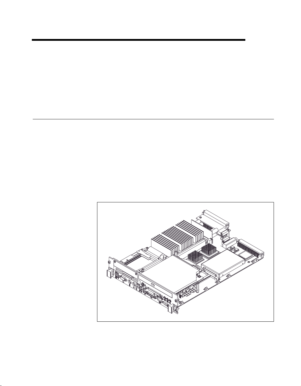
These three models differ in that the VXIpc-871 has an internal
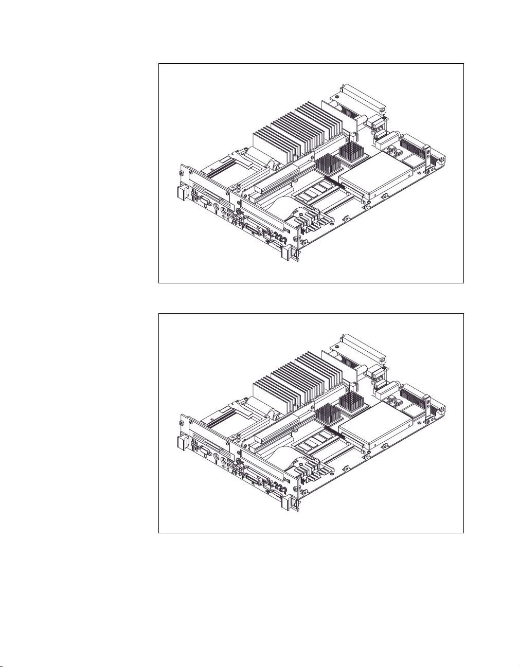
CD-ROM drive, while the VXIpc-872 has one AT/PCI expansion slot.
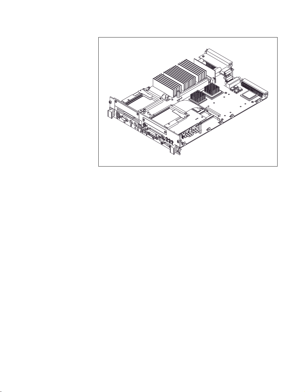
The VXIpc-873 has either an internal, nonremovable flash drive and one
AT/PCI expansion slot or a removable flash drive.
The following four figures show the models with their covers removed.
Refer to Appendix C, Front Panel and Connectors, for information about
the location and pinout assignment of each connector on the modules.
1
Figure 1-1. VXIpc-871 Embedded Controller
© National Instruments Corporation 1-1 VXIpc 870 Series User Manual
Page 14
Chapter 1 Introduction
Figure 1-2. VXIpc-872 Embedded Controller
Figure 1-3. VXIpc-873 Embedded Controller (Option 1 with
an Internal, Nonremovable Flash Drive)
VXIpc 870 Series User Manual 1-2 www.ni.com
Page 15
Chapter 1 Introduction
Figure 1-4. VXIpc-873 Embedded Controller (Option2 with a Removable Flash Drive)
The VXIpc 870 Series controllers are C-size, embedded computers based
on the x86 Processor architecture, the Peripheral Component Interface
(PCI) bus, and the Advanced Graphics Port (AGP). These computers
are high-performance, easy-to-use platforms for controlling VXIbus
systems, featuring complete VXI functionality through interactive
utilities and C function calls. In addition, the VXIpc 870 Series has
Ethernet capability plus an IEEE 488.2 interface that is compatible
with the NI-488.2 architecture.
The VXIpc 870 Series is a custom computer that you install directly in two
C-size slots of your VXI mainframe. An embedded computer can take full
advantage of the VXI high-performance backplane capabilities and give
you direct control of VXI registers, memory, interrupts, and triggers.
All models in the VXIpc 870 Series are fully VXIplug&play compliant
and are compatible with PC-compatible software tools, the National
Instruments LabVIEW and LabWindows/CVI application software, and
the NI-VXI, NI-VISA, and NI-488.2 bus interface software.
© National Instruments Corporation 1-3 VXIpc 870 Series User Manual
Page 16

Chapter 1 Introduction
Standard Equipment
Your hardware includes the VXIpc 870 Series controller, which you install
in your VXI mainframe. You also receive the following accessories:
• COM1/2 adapter cable
• Enhanced parallel port adapter cable
• Single-shielded 2 m GPIB cable
• AT-PS/2 cable
National Instruments Software
National Instruments has developed several software kits you can use
with the VXIpc 870 Series.
Driver Software
NI-VXI is the name of the National Instruments VXI bus control library.
You can create applications using NI-VXI to control both VXI and VME
devices. NI-VXI gives you complete VXI/VME functionality, including
an API for performing basic VXI/VME data transfers and handling
VXI/VME interrupts as well as VXI-specific functionality, such as
doing message-based communication and handling VXIbus triggers.
NI-VISA is the National Instruments implementation of the VISA
specification. VISA is a uniform API for communicating and controlling
Serial, GPIB, VXI, and VME instruments. This API aids in the creation of
more portable applications and instrument drivers.
The NI-VXI/VISA software includes an interactive configuration and
troubleshooting program, libraries of software routines for test and
measurement (T&M) programming, interactive control programs for both
NI-VXI and NI-VISA, a logging utility you can use for debugging your
applications, and a VXI Resource Manager. You can use this software to
seamlessly program multiple-mainframe configurations and have software
compatibility across a variety of controller platforms.
The NI-488.2M software kit gives you access to the industry-standard
NI-488.2M software for controlling external GPIB instruments through the
GPIB port on the front panel of your VXIpc 870 Series. The GPIB interface
on your VXIpc controller is fully compatible with the NI-488.2M driver for
a variety of operating systems. Any software using NI-488.2M will run on
the VXIpc 870 Series.
VXIpc 870 Series User Manual 1-4 www.ni.com
Page 17

Application Software
You can also use the National Instruments LabVIEW and
LabWindows/CVI application programs and instrument drivers to
ease your programming task. These standardized programs match the
modular virtual instrument capability of VXI and can reduce your VXI
software development time. These programs are fully VXIplug&play
compliant and feature extensive libraries of GPIB, Serial, and VXI
instrument drivers written to take full advantage of direct VXI control.
LabVIEW and LabWindows/CVI include all the tools needed for
instrument control, data acquisition, analysis, and presentation.
LabVIEW is a complete programming environment that departs from the
sequential nature of traditional programming languages and features a
graphical programming environment.
LabWindows/CVI is an interactive C development environment for
building test and measurement and instrument control systems. It includes
interactive code-generation tools and a graphical editor for building custom
user interfaces.
Chapter 1 Introduction
© National Instruments Corporation 1-5 VXIpc 870 Series User Manual
Page 18

Configuration and Installation
This chapter contains the instructions to configure and install the
VXIpc 870 Series. Unless otherwise noted, these instructions apply to
all models in the VXIpc 870 Series, which currently consists of the
VXIpc-871, VXIpc-872, and VXIpc-873.
2
Caution
Series module. To avoid such damage in handling the module, touch the antistatic plastic
package to a metal part of your VXI mainframe before removing the module from the
package.
Electrostatic discharge can damage several components on your VXIpc 870
What You Need to Get Started
❑
VXIpc 870 Series embedded controller
❑
VXIbus mainframe
❑
Keyboard
❑
Mouse
❑
Monitor with VGA or better resolution
❑
National Instruments software media for the VXIpc 870 Series
The NI-VXI/VISA software is already installed on your VXIpc 870 Series
computer. It is also included on CD-ROM in the event that you need to
reinstall your software. The CD-ROM includes disk images if you need to
make floppies for reinstallation.
Installing the VXIpc 870 Series
This section contains general installation instructions for the VXIpc 870
Series. Consult your VXIbus mainframe user manual or technical reference
manual for specific instructions and warnings.
1. Plug in your mainframe before installing the VXIpc 870 Series. The
power cord grounds the mainframe and protects it from electrical
damage while you are installing the module.
© National Instruments Corporation 2-1 VXIpc 870 Series User Manual
Page 19

Chapter 2 Configuration and Installation
Warning
To protect both yourself and the mainframe from electrical hazards,
the mainframe should remain off until you are finished installing the VXIpc 870 Series
module.
2. Remove or open any doors or covers blocking access to the mainframe
slots.
Caution
If the VXIpc 870 Series is not configured for automatic System Controller
detection, be certain that the slot you select in your VXIbus mainframe matches the
VXIpc 870 Series configuration as either a System Controller device or a Non-System
Controller device. Installing the VXIpc 870 Series into a slot that does not correspond
with the jumper setting can damage the VXIpc 870 Series, the VXIbus backplane, or both.
3. Insert the VXIpc 870 Series in the slot you have selected by aligning
the top and bottom of the module with the card-edge guides inside the
mainframe. Slowly push the VXIpc 870 Series straight into the slot
until its plug connectors are resting on the backplane receptacle
connectors. Using slow, evenly distributed pressure, press the module
straight in until it seats in the expansion slot. The front panel of the
VXIpc 870 Series should be even with the front panel of the
mainframe.
4. Tighten the retaining screws on the top and bottom edges of the front
panel.
5. Check the installation.
6. Connect the keyboard and mouse to the appropriate connectors.
Use the keyboard adapter cable that you received with your kit to adapt
AT-style keyboards to the VXIpc 870 Series mini-DIN connector.
7. Connect the VGA monitor video cable to the VGA connector.
8. Connect devices to ports as required by your system configuration.
Some ports, such as the COM and LPT ports, have adapter cables that
came in your kit.
9. Replace or close any doors or covers to the mainframe.
10. Turn on the VXI mainframe.
11. The VXIpc 870 Series should now boot into either Windows 98 or NT.
12. On the first boot of the VXIpc 870 Series, a setup program
automatically runs.
13. Follow the prompts in the setup program to fully configure your
VXIpc 870 Series.
14. When prompted for the NT/98 serial number, enter the serial number
of the operating system from the included certificate.
VXIpc 870 Series User Manual 2-2 www.ni.com
Page 20

Chapter 2 Configuration and Installation
15. The next prompt asks if you purchased LabVIEW or
LabWindows/CVI. Select the appropriate boxes and insert the
disks when prompted.
16. Your VXIpc 870 Series is now ready for development.
17. Refer to Chapter 4, Developing Your Application,formore
information.
Installing and Removing Flash Memory in the VXIpc-873
If your VXIpc-873 has removable flash memory, follow these instructions
to install and remove the flash storage card.
Installing the Flash Storage Card
1. Turn off the VXI mainframe.
Warning
Failure to turn off the mainframe will damage the VXIpc-873, the storage card, or both.
Always turn off the mainframe while installing or removing the flash memory.
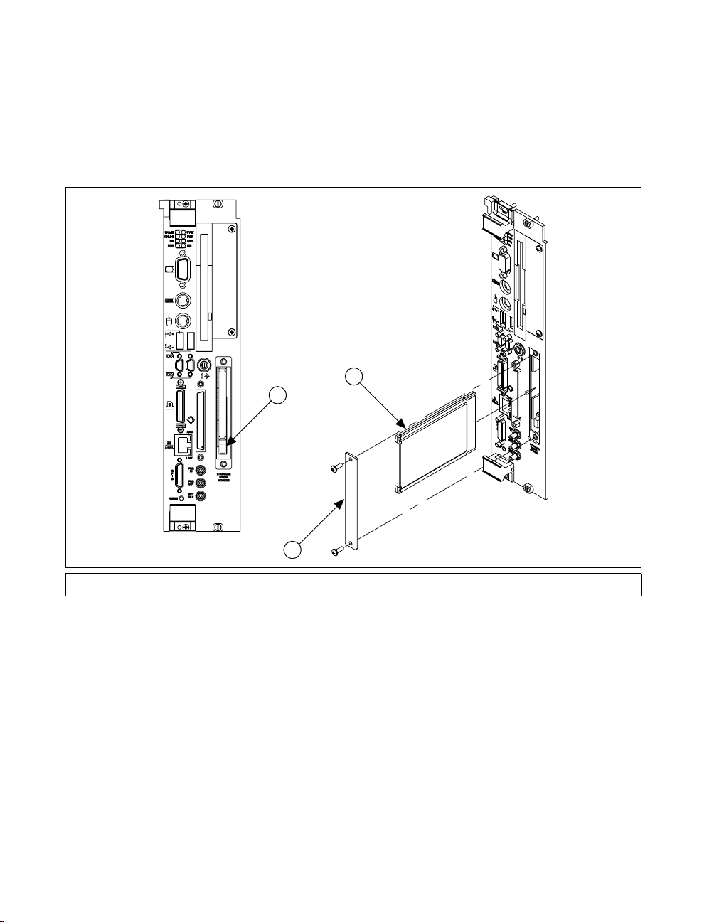
2. Remove the two screws and cover panel on the VXIpc-873 as shown
in Figure 2-1.
3. Align the connector end of the flash storage card with the flash storage
card carrier.
4. Slide the card into the carrier until you feel resistance. Press the card
firmly into the carrier until the ejector button at the bottom of the drive
slot slides forward.
5. Reinstall the cover plate and screws.
Removing the Flash Storage Card
1. Turn off the VXI mainframe.
Warning
Failure to turn off the mainframe will damage the VXIpc-873, the storage card, or both.
Always turn off the mainframe while installing or removing the flash memory.
2. Remove the two screws and cover panel on the VXIpc-873 as shown
in Figure 2-1.
© National Instruments Corporation 2-3 VXIpc 870 Series User Manual
Page 21
Chapter 2 Configuration and Installation
3. Press the ejector button at the bottom of the flash drive carrier slot until
the flash storage card pops out of the drive.
4. Slide the card out of the drive.
Reinstall the cover plate and screws.
2
1
3
1 Ejector Button 2 Type I or II Flash Storage Card 3 Cover Panel
Figure 2-1. Installing and Removing a Flash Storage Card
VXIpc 870 Series User Manual 2-4 www.ni.com
Page 22
Configuration and Default Settings
Hardware Default Settings
This chapter summarizes the hardware default settings for the VXIpc 870
Series for easy reference. The module is set at the factory for the most
commonly used configuration.
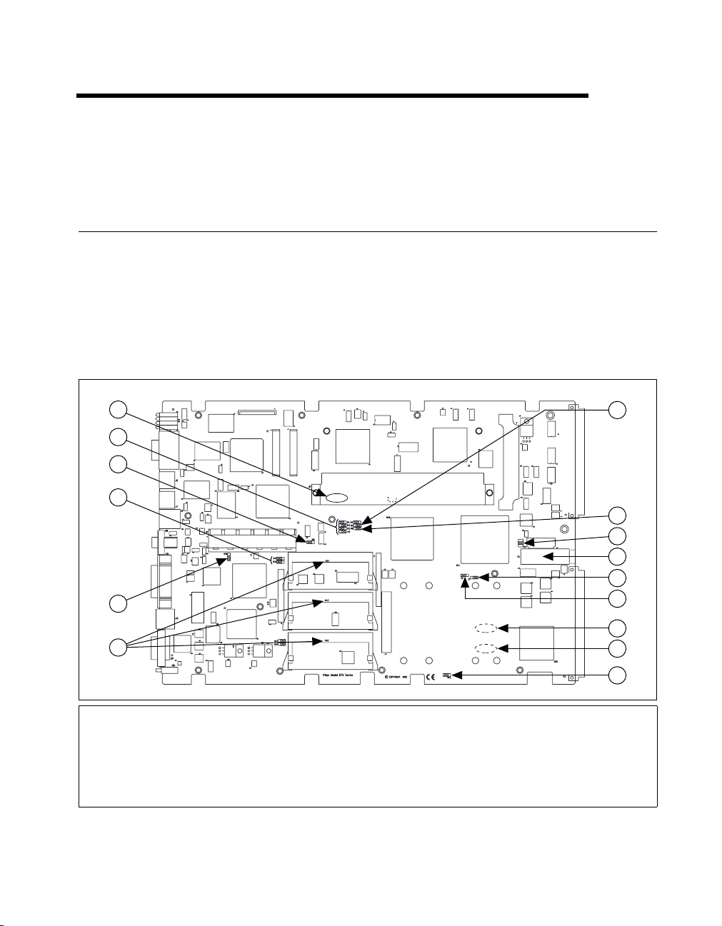
Figure 3-1 shows the location of the user-configurable jumpers and
switches on the VXIpc 870 Series. The diagram also shows the location
of the serial and assembly numbers.
3
1
2
3
4
5
6
1 Ethernet Address
2 CPU Bus Factor (W1, W3, W5, W7)
3FlashProtect(W8)
4 SCSI Termination Enable (W11-W12)
5 Ethernet Serial EEPROM Enable (W10)
6SO-DIMMSockets
7 Bus Speed (W4)
8CMOS(W6)
9 Automatic Slot Detection
(J22)
10 Fuse Location
Figure 3-1. VXIpc 870 Series Parts Locator Diagram
11 MITE User Configuration (S1)
12 MITE Configuration Enable (S2)
13 Assembly Number (Back Side)
14 Serial Number (Back Side)
15 Power Monitor (W15)
7
8
9
10
11
12
13
14
15
© National Instruments Corporation 3-1 VXIpc 870 Series User Manual
Page 23

Chapter 3 Configuration and Default Settings
Table 3-1 lists the factory-default settings and options for the onboard
jumpers and switches.
Jumper Default Setting Optional Setting
Table 3-1. VXIpc 870 Series Hardware Default Settings
J12 Enable automatic Slot 0
detection
S1 MITE user configuration MITE factory configuration
S2 Enable MITE
self-configuration
W1,3,5,7 CPU bus factor
W4 100 MHz CPU bus speed 66 MHz CPU bus speed
W6 Normal CMOS operation Clear CMOS
W8 Flash write enable Flash protection
W10 Enable Ethernet Serial
EEPROM configuration
W11-12 Enable 16-bit SCSI
termination
W15 Voltage monitor
only required voltages
Force Slot 0;
Force Non-Slot 0
Disable MITE
self-configuration
Note: Refer to CPU Bus
Factor section later in this
chapter.
Disable Ethernet Serial
EEPROM configuration
(uses default power on
values)
SCSI termination
Voltage monitor
all voltages
Note
Please do not adjust any jumpers or switches not listed in Table 3-1 or that are not
documented in this manual unless directed by National Instruments. Other configuration
jumpers are shown in the event National Instruments Technical Support needs to make
adjustments to your settings.
Software Default Settings
In this section, Tables 3-2 through 3-4 contain summaries of default
settings for VXIpc T&M Explorer. Because you can also use T&M Explorer
VXIpc 870 Series User Manual 3-2 www.ni.com
Page 24

Chapter 3 Configuration and Default Settings
to configure a VXI-MXI-2, for your convenience, Tables 3-5 through 3-7
contain a summary of the software default settings for the VXI-MXI-2.
Table 3-2. VXIpc T&M Explorer Device Tab Default Settings
Editor Field Default Setting
Logical address 0
Device class Message based
Size of Servant area 0
Number of handlers 1
Number of interrupters 0
Table 3-3. VXIpc T&M Explorer Shared Memory Tab Default Settings
Editor Field Default Setting
Memory sharing A32
Shared RAM size 64 KB (when sharing memory)
Reserved physical memory 64 KB (when sharing memory)
Lower half window byte swapping Disabled
Upper half window byte swapping Disabled
Map upper and lower halves at
Disabled
same PCI address
Table 3-4. VXIpc T&M Explorer PCI Tab Default Settings
Editor Field Default Setting
Low-level register access API
Enabled
support
User window size 128 MB
VXI-MXI-2
This section summarizes the software default settings for the VXI-MXI-2.
This information is included for your convenience in case you have any of
these modules in your system.
© National Instruments Corporation 3-3 VXIpc 870 Series User Manual
Page 25

Chapter 3 Configuration and Default Settings
Table 3-5. VXI-MXI-2 T&M Explorer Device Tab Default Settings
Editor Field Default Setting
Logical address
Address space
Requested memory
A24/A32 write posting
A16 write posting
Interlocked mode
* Assumes no DRAM is installed. If DRAM is installed, the Address space should be
A32, and Requested memory should match the amount of DRAM. If you install the
DRAM yourself, you must manually specify these changes.
Table 3-6. VXI-MXI-2 T&M Explorer VXI Bus Tab Default Settings
Use DIP switch
A24 *
16 KB *
Disabled
Disabled
Disabled
Editor Field Default Setting
Bus timeout value
Slot 0 configuration
Auto retry
Transfer limit
Arbiter type
125 µs
Auto-detect
Disabled
256
Priority
Fair requester
Arbiter timeout
Request level
VXIpc 870 Series User Manual 3-4 www.ni.com
Enabled
Enabled
3
Page 26

Chapter 3 Configuration and Default Settings
Table 3-7.
System controller
Bus timeout value
MXI-2 auto retry
MXI transfer limit
MXI fair requester
Perform parity checking
MXI-2 CLK10 signal direction
VXI-MXI-2 T&M Explorer MXI-2 Bus Tab Default Settings
Editor Field Default Setting
Configuring the VXIpc 870 Series
This section describes how to configure the following options on the
VXIpc 870 Series:
• VXI Controller/Non-System Controller
• VXIbus CLK10 routing and termination
• Trigger input termination
• MITE EEPROM
Auto-detect
1ms
Disabled
Unlimited
Disabled
Enabled
Switch determines signal
direction
Accessing the Hardware Switches
The VXIpc 870 Series is housed in a metal enclosure comprised of a top
and bottom cover to improve EMC performance and to provide easy
handling. You need to remove the top cover to change many of the switch
and jumper settings. You must also remove the top cover to change the
amount of DRAM installed on the module.
Remove the top cover by removing the screws that attach it to the module.
© National Instruments Corporation 3-5 VXIpc 870 Series User Manual
Page 27
Chapter 3 Configuration and Default Settings
VXIbus System Controller/Non-System Controller
The VXIpc 870 Series is configured at the factory to automatically detect
if it is installed in Slot 0 of a VXIbus mainframe. With automatic System
Controller slot detection, you can install the module into any VXIbus slot.
You can manually configure the VXIpc 870 Series for either System
Controller or Non-System Controller operation by defeating the
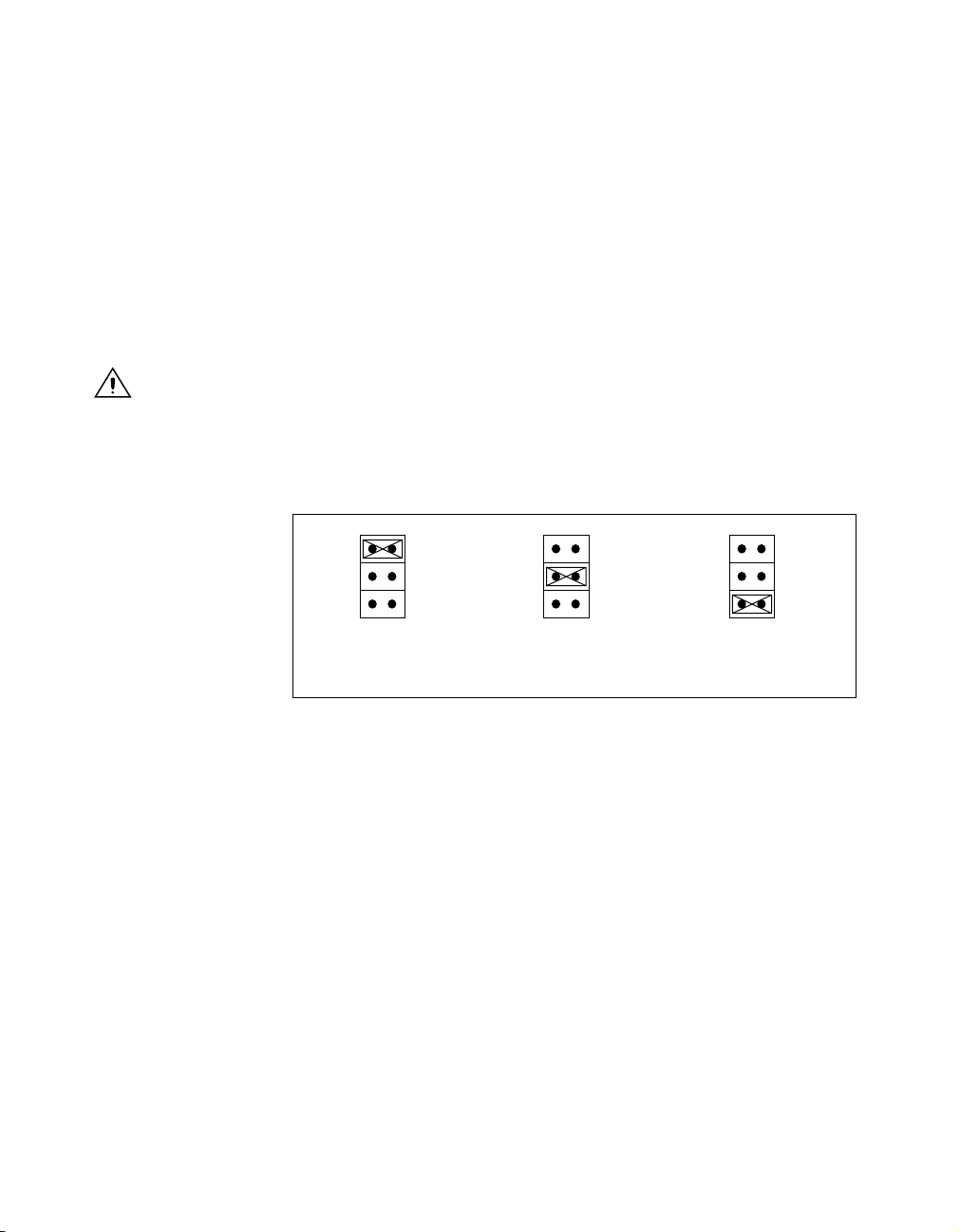
automatic-detection circuitry. Use the three-position jumper J12 to select
automatic detection, System Controller, or Non-System Controller
operation. Figure 3-2 shows these three settings.
Caution
Do not install a device configured for System Controller into another slot
without first reconfiguring it to either Non-System Controller or automatic-detection
configuration. Neglecting to do this could result in damage to the device, the VXIbus
backplane, or both.
J12
a. Manual Slot 0
Configuration
Figure 3-2. System Controller Slot Configuration
b. Automatic Slot 0
Detection (Default)
J12
J12
c. Manual Non-Slot 0
Configuration
When the VXIpc 870 Series is installed in Slot 0 of a VXI system, it
becomes the VXIbus System Controller. In this role, it has VXIbus Data
Transfer Bus Arbiter circuitry that accepts bus requests on all four VXIbus
request levels, prioritizes the requests, and grants the bus to the highest
priority requester. As VXIbus System Controller, the VXIpc 870 Series
also drives the 16 MHz VXIbus system clock by an onboard 16 MHz
oscillator.
As required by the VXIbus specification, the VXIpc 870 Series drives
the 10 MHz signal CLK10 on a differential ECL output when installed in
Slot 0. When not installed in Slot 0, the VXIpc 870 Series only receives
the CLK10 signal.
VXIpc 870 Series User Manual 3-6 www.ni.com
Page 28

VXIbus CLK10 Routing and Termination
When the VXIpc 870 Series is installed in Slot 0 of your mainframe, it
supplies the VXIbus CLK10 signal. The VXIpc 870 Series can use two
different sources to generate this signal—an onboard oscillator or the
external CLK SMB connector. The VXIpc 870 Series can also be
configured to drive the external CLK10 SMB from the VXIbus CLK10
signal when in Non-Slot 0.
The VXIpc 870 Series has onboard logic that helps configure the VXIbus
CLK10 routing and termination. You can route the CLK10 signal from
the front panel to the backplane or from the backplane to the front panel.
Youalsohavetheoptiontoadda50Ω termination to the signal.
All settings for CLK10 routing and termination are handled through
software. Use T&M Explorer to configure these settings.
Trigger Input Termination
You have the option to terminate the external trigger input SMB with 50 Ω
to ground to match the driving source, if necessary. Use T&M Explorer to
set this option.
Chapter 3 Configuration and Default Settings
MITE EEPROM
The VXIpc 870 Series has an onboard EEPROM, which stores default
register values for the VXI circuitry. These values are loaded when you
power up the computer. These values read from the EEPROM program the
PCI interface and the VXIbus registers so that the VXI interface is ready
to respond to Resource Manager accesses within the required 5 s of
SYSRST* deasserting.
You can disable this power-on self-configuration (POSC) circuit by
changing switch S2. Although this makes the VXI circuitry unusable, it
is sometimes helpful in debugging address and interrupt conflicts with
add-in boards. In general, however, you should leave switch S2 in its
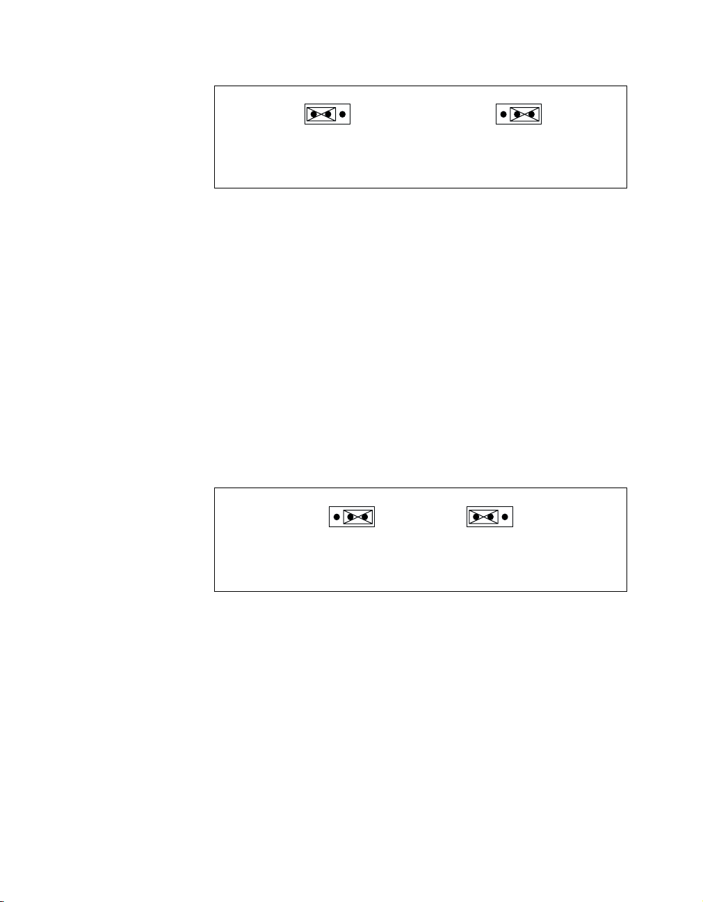
factory-default setting. Figure 3-3 shows the possible configurations
for S2.
© National Instruments Corporation 3-7 VXIpc 870 Series User Manual
Page 29
Chapter 3 Configuration and Default Settings
S2
a. VXI Circuitry Loads Power-on
Defaults from EEPROM (Default)
Figure 3-3. Power-on Self Configuration Status
b. Power-on Self Configuration
S2
Circuit is Disabled
The EEPROM is divided into two halves—one half is factory configured
and one half is user configurable. Use switch S1 to control the operation
of the EEPROM. The setting of this switch determines whether the
VXIpc 870 Series boots off the factory-configured half or the
user-modified settings. In its default setting, the VXIpc 870 Series
boots off the user-configurable half.
This switch is useful in the event that the user-configured half of the
EEPROM becomes corrupted in such a way that the VXIpc 870 Series
boots to an unusable state. By altering this switch setting, you can return to
the factory configuration and get up and running again. Use the procedure
as described in the following section, HowtoFixanInvalidEEPROM
Configuration.
Figure 3-4 shows the configuration settings for EEPROM operation.
S1 S1
a. Boot from User
Configuration (Default)
b. Boot from Protected
Configuration
Figure 3-4. EEPROM Configuration
How to Fix an Invalid EEPROM Configuration
Use T&M Explorer under Windows NT/9x to edit the configuration of the
VXIpc 870 Series. Some of these settings are stored in files that are read
by the NI-VXI software, while other settings are stored directly in the
VXIpc 870 Series EEPROM.
Certain EEPROM configurations, including invalid configurations, can
lock up your computer while it is booting up. Generally, only the size and
location of the memory windows can cause your VXIpc 870 Series to lock
up your system. For example, many PCI-based computers will not boot if a
VXIpc 870 Series User Manual 3-8 www.ni.com
Page 30

Chapter 3 Configuration and Default Settings
board in its system requests more memory space than the computer can
allocate. If you encounter this situation you should reduce the size of the
VXIpc 870 Series user window. The EEPROM can become corrupted if
the VXIpc 870 Series is shut down while it is updating the EEPROM.
If this situation occurs after you change the configuration, perform the
following steps to reconfigure the VXIpc 870 Series:
1. Turn off your computer.
Warning
the mainframe should remain off until you are finished changing the settings on
the VXIpc 870 Series.
To protect both yourself and the mainframe from electrical hazards,
2. Change switch S1 to the position shown in Figure 3-4b to restore the
factory configuration.
3. Turn on the computer. The computer should boot this time because the
factory-default configuration is being used to initialize the VXIpc 870
Series.
4. Run your software configuration utility to re-adjust the VXIpc 870
Series configuration.
5. After saving the configuration, exit Windows and turn off the
computer.
6. Change switch S1 to the default position, as shown in Figure 3-4a.
7. Turn on the computer. If the computer does not boot with this
configuration, you will need to repeat these steps, modifying your
configuration until a final configuration is reached.
Configuring the PC
This section describes how to configure the following options on the PC:
• SCSI termination
• System CMOS
• CPU bus speed
• CPU bus factor
• Flash Protection
• Ethernet Serial EEPROM
• Voltage Monitor
© National Instruments Corporation 3-9 VXIpc 870 Series User Manual
Page 31
Chapter 3 Configuration and Default Settings
• NI WatchDOG
• Installing additional memory
This section also explains how to change the main power fuse.
SCSI Termination
The VXIpc 870 Series uses active termination on the SCSI-3 bus. Because
the VXIpc 870 Series is always an end device, you should not need to
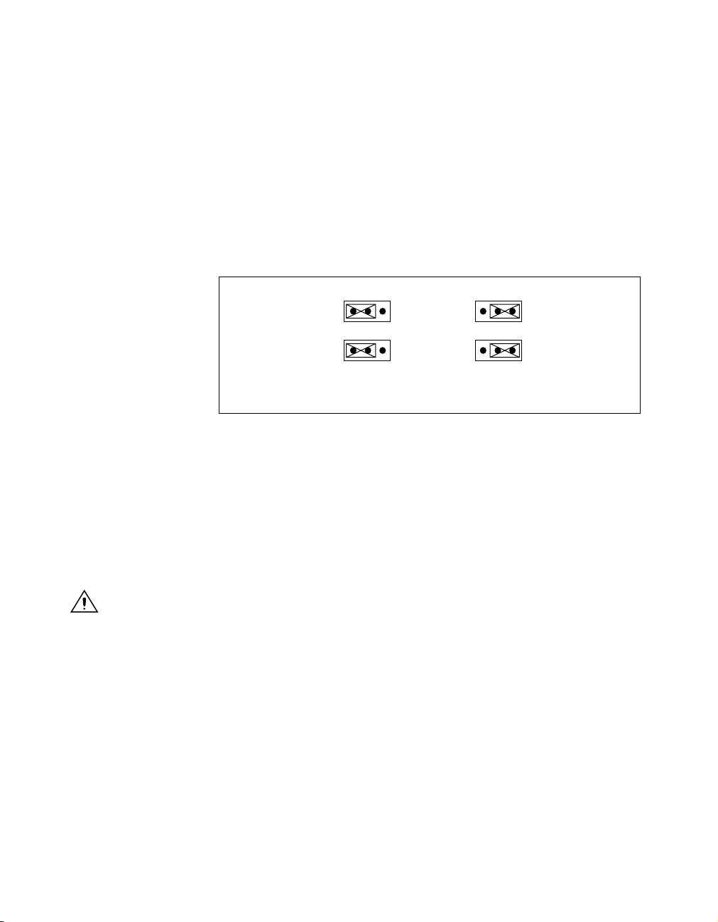
disable the termination; however, for informational purposes Figure 3-5
shows the jumper settings for both enabled and disabled termination.
System CMOS
Caution
sustained when the power is turned off in this state.
W11
W12
a. Terminate SCSI
Signals (Default)
Figure 3-5. SCSI Termination
W11
W12
b. Do Not Terminate
SCSI Signals
The VXIpc 870 Series contains a backed-up memory used to store BIOS
defaults and configuration information:
To clear the CMOS contents:
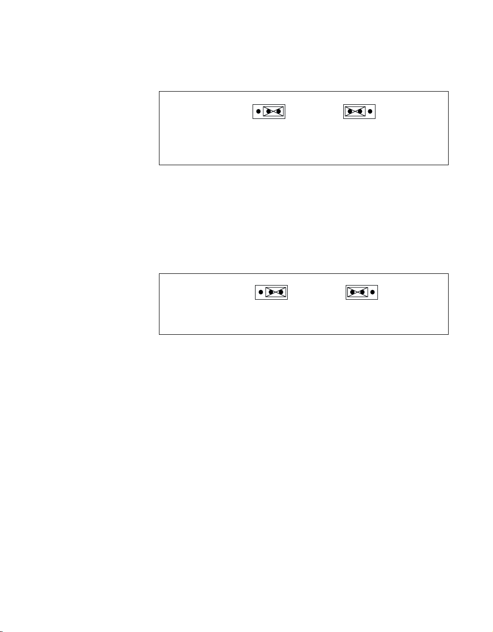
1. Place the jumper as shown in Figure 3-6b to short the pins of W6.
Do not keep these two pins shorted because the CMOS memory cannot be
2. Power-on the VXIpc 870 Series. The screen should briefly appear,
andthengoblack.
3. Power-off the VXIpc 870 Series.
VXIpc 870 Series User Manual 3-10 www.ni.com
Page 32
Chapter 3 Configuration and Default Settings
4. Remove the jumper as shown in Figure 3-6a to restore normal
operation.
CPU Bus Speed
W6
a. Normal Operation
(Default)
Figure 3-6.
System CMOS
W6
b. Clear CMOS
Contents
The VXIpc 870 Series supports CPU bus speeds at 66 MHz and 100 MHz.
Under most circumstances 100 MHz delivers the best performance.
However, if you want to use a lower bus speed, W4 overrides the 100 MHz
setting as shown in Figure 3-7.
W4
a. 100 MHz (Default) b. 66 MHz
Figure 3-7.
CPU Bus Speed Configuration
W4
© National Instruments Corporation 3-11 VXIpc 870 Series User Manual
Page 33
Chapter 3 Configuration and Default Settings
CPU Bus Factor
All Pentium II CPUs are supported as of the release date of this document.
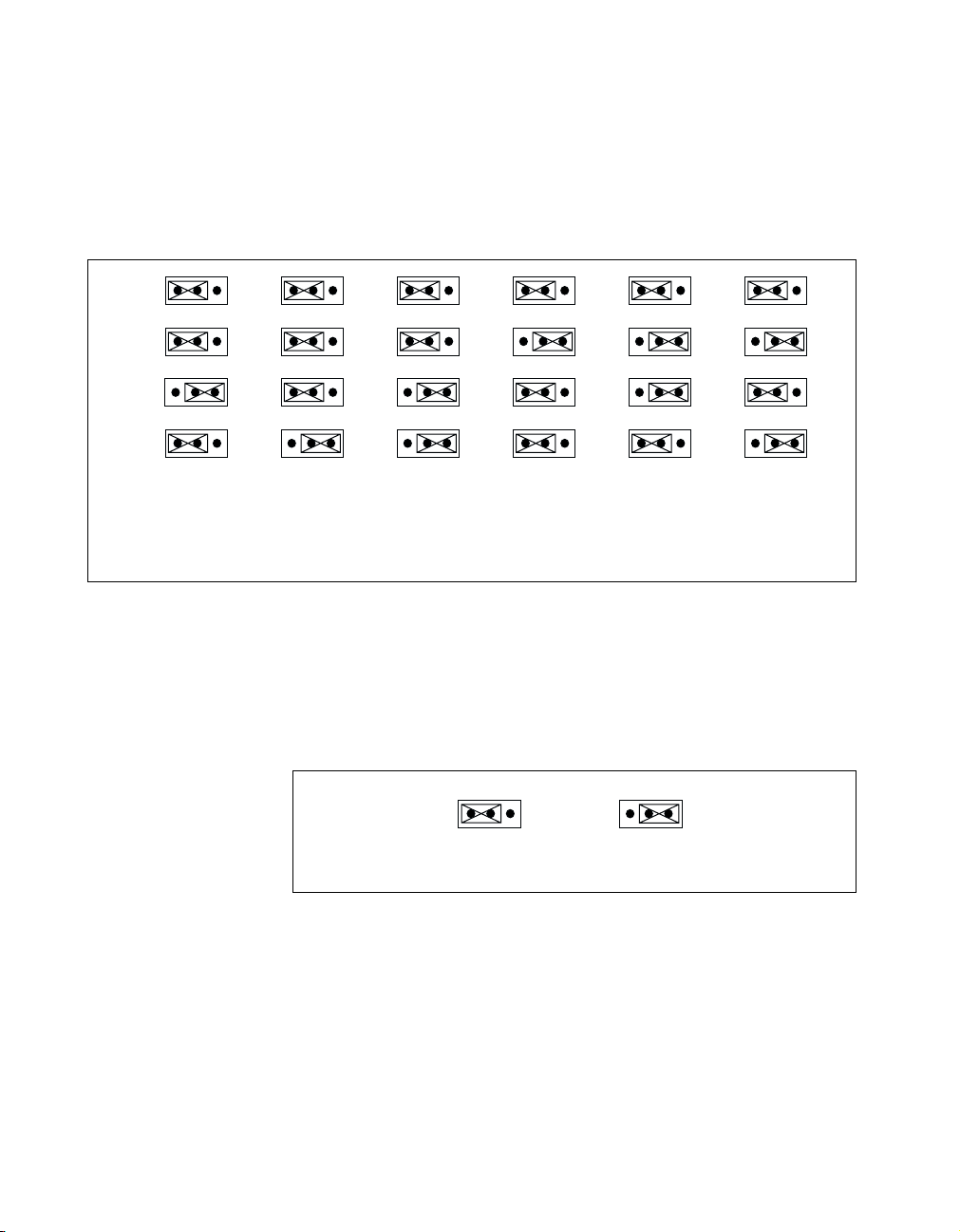
The jumper settings in Figure 3-8 are provided to allow the user to upgrade
as newer CPUs enter the market. Contact National Instruments for jumper
settings as new CPUs are released.
W1
W3
W7
CPU
Speed
Factor
300 MHz
x3Bus
Flash Protection
W1 W1 W1
W3
W5
W7
400 MHz
x4
W3
W5W5
W7
500 MHz
x5
250 MHz
x2.5
W3
W5
W7
W1
W3
W5
W7
350 MHz
x3.5
W1
W3
W5
W7
450 MHz
x4.5
(default)
Figure 3-8. CPU Bus Factor Jumper Settings
The VXIpc 870 Series uses a standard 2M bit flash with write protection.
Under normal use, this jumper should not be changed. Figure 3-9 shows
default and disabled settings.
W8 W8
a. Flash Write
Enabled (Default)
b. Flash Write
Disabled
Figure 3-9. Flash Protection Settings
VXIpc 870 Series User Manual 3-12 www.ni.com
Page 34
Ethernet Serial EEPROM
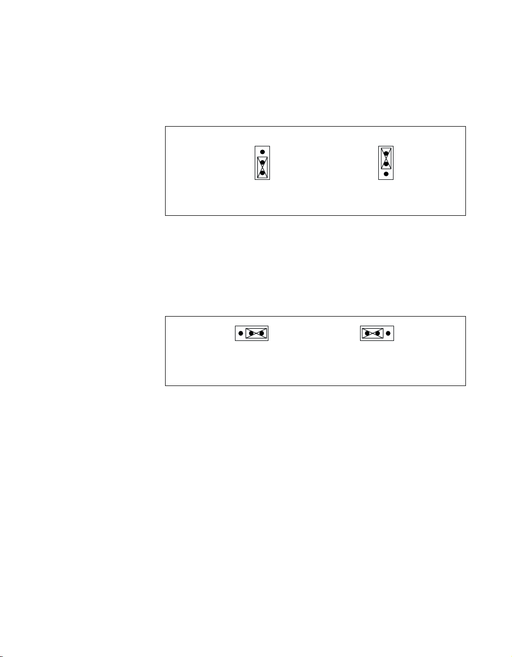
A serial EEPROM loads the Ethernet power-on settings. Under normal use,
this jumper should not be changed. Figure 3-10 shows default and disabled
settings.
Chapter 3 Configuration and Default Settings
Voltage Monitor
NI WatchDOG
W10
a. Ethernet Serial EEPROM
Enabled (Default)
Figure 3-10. Ethernet Serial EEPROM Settings
b. Ethernet Serial EEPROM
W10
Disabled
You can monitor all backplane voltages or only those required to boot on
the VXIpc 870 Series with built-in voltage-monitor circuitry as shown in
Figure 3-11.
W15
a. Voltage Monitor Only Those
Required by 870 (Default)
Figure 3-11.
Voltage Monitor Settings
b. Monitor All VXI Voltages
W15
The NI WatchDOG is an onboard, general-purpose counter/timer. You can
it use to monitor running applications and reset the embedded controller or
assert a signal should the system lock up. All WatchDOG timer features are
configured through T&M Explorer. See the NI WatchDOG section in
Chapter 5, Functional Overview, for more information.
Installing Additional Memory
The VXIpc 870 Series uses 144 pin 100 MHz SDRAM and supports 16, 32,
64, and 128 MB SO-DIMMs for a total of 384 MB maximum. As DRAM
technology improves, the maximum amount of RAM supported may
increase.
© National Instruments Corporation 3-13 VXIpc 870 Series User Manual
Page 35
Chapter 3 Configuration and Default Settings
To add RAM to the VXIpc 870 Series, do the following.
1. Remove the unit from the VXI mainframe.
2. Remove the screws that hold the cover in place and remove the cover.
3. Add SO-DIMM modules to the empty SO-DIMM sockets.
National Instruments recommends the following types of SO-DIMMs for
use with the VXIpc 870 Series controller (SDRAM):
32 MB: 4 MB × 64 SO-DIMMs—10 ns, 1.05 in. max.
64 MB: 8 MB × 64 SO-DIMMs—10 ns, 1.05 in. max.
128 MB: 16 MB × 64 SO-DIMMs—10 ns, 1.05 in. max.
Note
National Instruments has tested and verified that the SO-DIMMs we sell work
with the VXIpc 870 Series. We recommend you purchase your SO-DIMM modules from
National Instruments. Other off-the-shelf SO-DIMM modules are not guaranteed to work
properly.
Changing the Main Power Fuse
The VXIpc 870 Series is equipped with a user-replaceable fuse on the
main power, +5 V from the VXIbus. All other voltages are fused with a
resettable-style circuit breaker. The resettable-style circuit breakers do not
require user intervention. When a short circuit condition is removed, they
automatically reset themselves.
The main power, +5 V, is too high of a current for resettable fuse
technology, so your kit includes a replaceable fuse of type 3AG, 15A,
Slowblow.
You can replace this fuse without having to remove the cover. The fuse is
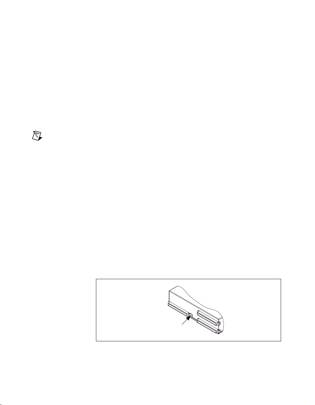
accessible through the rear of the unit as shown in Figure 3-12.
Fuse Holder
Figure 3-12. Main Power Fuse Replacement
VXIpc 870 Series User Manual 3-14 www.ni.com
Page 36

Chapter 3 Configuration and Default Settings
To replace a fuse, do the following:
1. Turn off the VXI mainframe and remove the VXIpc 870 Series
module.
2. Using a small flathead screwdriver, turn the fuse holder
counter-clockwise until the fuse and holder start to come out of
the unit.
3. Replace the fuse with the same type fuse.
Caution
Do not replace with a higher-rated fuse. This could cause damage to the
VXIpc 870, the VXI mainframe, or both.
4. Insert the fuse and hold back into the fuse housing, pushing it all the
way in.
5. Screw the fuse holder clockwise until the fuse holder is flush with the
fuse housing.
6. Re-install the VXIpc 870 and apply power.
Note
If the fuse continues to blow, contact National Instruments for assistance.
© National Instruments Corporation 3-15 VXIpc 870 Series User Manual
Page 37

Developing Your Application
This chapter discusses the software utilities you can use to start developing
applications that use the NI-VXI/VISA driver.
After verifying your system configuration, you can begin to develop your
VXI/VME or VISA application software. Be sure to check the
README.txt
Your software includes several utilities to assist you in your system
development. These include T&M Explorer, Resman, NI Spy, VISAIC, and
VIC. You can also access several examples to learn how to use NI-VISA or
NI-VXI for certain tasks. Each of these components assists you with one of
four steps of development: configuration, device interaction, programming,
and debugging.
You can access these utilities through the Windows Start menu. Open
either the National Instruments VXI or VXIpnp program group and select
the utility you want to use.
file for the latest application development notes and changes.
4
Configuration
The configuration utilities in your kit are T&M Explorer and Resman.
Resman is the application that performs VXI Resource Manager functions
as described in the VXIbus specification. Its most important functions
include configuring all VXI devices on the VXI backplane for operation
and allocating memory for devices that request it.
Note
Because power cycling resets all devices, run Resman to reconfigure them every
time chassis power is cycled.
Resman must be run on any system that contains VXI devices
(including systems containing VXI-MXI-2 or VME-MXI-2 mainframe
extender devices). Because VME devices normally do not have
configuration registers as defined in the VXIbus specification, the
Resource Manager is unable to detect VME devices. Because of this,
when using systems containing a mixture of VME devices and VXI
devices, you need to manually add your VME devices in T&M Explorer
© National Instruments Corporation 4-1 VXIpc 870 Series User Manual
Page 38

Chapter 4 Developing Your Application
using the Add VME Device Wizard to reserve system resources when the
Resource Manager runs.
Systems consisting of only a VMEpc 870 Series controller, a VME chassis,
and VME boards do not need to run Resman when using NI-VXI software
even though the devices do not appear in the T&M Explorer connection
tree. However, you would not be able to use VISA without manually
adding the VME devices to the system by using T&M Explorer as
described above and then running Resman. This is because NI-VISA uses
the Resource Manager to create instrument sessions for VXI/VME device
communication. If this is not an issue for you, you can skip Resman.
T&M Explorer presents a graphical display of your entire test and
measurement system to help you configure various components. When
you launch T&M Explorer, you see all your VXI, GPIB, GPIB-VXI, and
serial devices on the screen. You can add devices that cannot be detected
dynamically by T&M Explorer through the Add Device Wizard in the
Edit menu. Such devices include VME devices, certain GPIB devices, and
serial ports. You can view the properties (such as logical address, address
space used, primary address, and so on) of each device by right-clicking
on the device in the tree. When you view the properties of most National
Instruments devices, you can configure the hardware settings directly in the
property pages.
T&M Explorer and Resman are designed to work together. You can run the
Resource Manager through T&M Explorer by either clicking on the Run
Resman button on the toolbar, or selecting VXI Resource Manager from
the Tools menu. From the Options dialog in the Tools menu, you can also
configure T&M Explorer to run Resman automatically when the computer
boots up. Resman reports all errors that it finds in your system to T&M
Explorer. When you view your system through T&M Explorer, you can
easily spot any errors in your system that Resman found.
You can find more information about T&M Explorer by using its online
help. From T&M Explorer, open the Help menu and select Help Topics.
Device Interaction
After Resman has detected and configured all VXI devices, you can view
specific information on each device in your system by using the T&M
Explorer utility. This utility includes a System View, which contains a
description for each device, including each VXI device’s logical address.
VXIpc 870 Series User Manual 4-2 www.ni.com
Page 39

Chapter 4 Developing Your Application
You can interact with your VXI devices by using the VIC or VISAIC utility
(VIC for NI-VXI or VISAIC for NI-VISA). You can use these utilities to
interactively control your devices without having to use a conventional
programming language, LabVIEW, or LabWindows/CVI.
Note
You can launch VIC or VISAIC from the Tools menu in T&M Explorer.
Try the following in VIC:
In the Command entry field, type
help vxiin
.
This help file shows you the syntax for this command, which reads VME
address space. The first argument is the access parameters for selecting the
address space, byte order, and so on. The second is the VME address to
read, and the third is the width of the data to read.
Type:
vxiin 1,0xC000,2
The History window shows the result of the command execution, such as:
Return Status (0): SUCCESS.
value = 0x9ff6
If the value ends with
, you have successfully read the National
ff6
Instruments manufacturer ID from the VXIpc 870 Series ID register.
Because this is the first configuration register present for all VXI devices,
the VXI device at Logical Address 0 has its manufacturer ID register
located at A16 address 0xC000—the beginning of the VXI configuration
space.
You may now want to read the registers from other devices in your system
using the command
. Try reading a register from each of the devices
vxiin
listed in the Address Map View of T&M Explorer. In this way, you can
verify that your VXIpc 870 Series controller can access each of the devices
in your system successfully.
Alternatively, you can use VISAIC to interact with your devices.
VISAIC lists theavailable devices, similar to what T&M Explorer displays.
By double-clicking on a given device, you can open a VISA session and
access the device through it. For more information regarding VISAIC, use
the right-click help available from all panels.
© National Instruments Corporation 4-3 VXIpc 870 Series User Manual
Page 40

Chapter 4 Developing Your Application
Programming with VXI
National Instruments provides two different programming interfaces
for accessing your instruments: NI-VISA and NI-VXI. NI-VISA is the
National Instruments implementation of the VISA API as defined by the
VXIplug&play standard. It is very useful when you have different types
of instruments in your system (such as VXI, VME, GPIB, and Serial
devices) because the NI-VISA functions have the same interface.
NI-VXI is the National Instruments proprietary interface for programming
VXI/VME instruments. Both NI-VXI and NI-VISA grant you
register-level access of VXI/VME instruments as well as messaging
capability to message-based devices. With either interface you can service
asynchronous events, such as triggers and interrupts, and also assert them.
The best way to learn how to program with NI-VXI or NI-VISA is by
reviewing the example programs included in your software. In the
Examples
applications. If you are just getting started, you should first learn how to
access registers with high-level calls and send messages with word serial
functions. The NI-VISA examples of these tasks are called
and
VXIws.c
techniques. Consult the NI-VISA User Manual or the NI-VXI User Manual
for additional information on these topics.
directory you will find examples for many different types of
VISAws.c
. You should use the other examples as you try more advanced
. The NI-VXI examples are called
VISAhigh.c
VXIhigh.c
and
Note
The NI-VXI User Manual resides in the
NI-VISA User Manual is in the
would be either
Win95orWinNT
NIVXI\manuals
VXIpnp\os\NIvisa\manuals
. Use the Acrobat Reader program to open and navigate
directory, and the
directory, where
os
through the manuals.
Table 4-1 summarizes the topics addressed by the example programs.
Table 4-1. NI-VXI/VISA Examples
NI-VISA
Coverage
Message-Based Access
High-Level Register Access
Low-Level Register Access
Sharing Memory
VXIpc 870 Series User Manual 4-4 www.ni.com
Example
VISAws.c VXIws.c
VISAhigh.c VXIhigh.c
VISAlow.c VXIlow.c
VISAmem.c VXImem.c
NI-VXI Example
Page 41

Chapter 4 Developing Your Application
Table 4-1. NI-VXI/VISA Examples (Continued)
NI-VISA
Coverage
Example
NI-VXI Example
Interrupt Handling
Trigger Handling
Note
T&M Explorer includes special settings that you must use for low-level functions
and memory sharing. Consult the T&M Explorer online help for information on setting
these up.
Notes about VME Support
To use VME devices in your system, configure NI-VXI to see these devices
by using the Add Device Wizard in T&M Explorer. VME devices with
two blocks of memory in the same address space require two entries.
You can also specify which interrupt levels the device uses. VXI and VME
devices cannot share interrupt levels. You can then access the VME device
from NI-VXI or NI-VISA just as you would a register-based VXI device,
by specifying the address space and the offset from the base at which you
have configured it. NI-VISA support for VME devices includes the register
access operations (both high-level and low-level) and the block move
operations, as well as the ability to receive interrupts.
Compiler Symbols for NI-VXI
You may need to define some symbols so that the NI-VXI library can work
properly with your program.
VISAint.c VXIint.c
VISAtrig.c VXItrig.c
Note
Skip this section if you are programming with NI-VISA only. NI-VISA does not use
these symbols.
You can define the symbols using
or you can use either the
/D
#define
or the-Doption in your compiler (both the
Microsoft and Borland compilers support the
use
#define
the NI-VXI header file
statements, you must define the symbols before including
nivxi.h
. If you use the makefiles to compile the
statements in the source code
and-Doptions). If you
/D
sample program, the makefile already defines the necessary symbols.
The
Microsoft C or Borland C compiler.
symbol is required. You must define it when using the
VXINT
designates the application as
VXINT
a Windows NT/98 application.
© National Instruments Corporation 4-5 VXIpc 870 Series User Manual
Page 42

Chapter 4 Developing Your Application
Note
LabWindows/CVI automatically defines the correct symbol. You do not need to
define
when using LabWindows/CVI.
VXINT
Debugging
NI Spy, VISAIC, and VIC are useful utilities that can aid in identifying the
causes of problems in your application.
NI Spy tracks the calls your application makes to National Instruments
T&M drivers including NI-VXI, NI-VISA, and NI-488.2. NI-488.2 users
may notice that NI Spy is very similar to GPIB Spy. It highlights functions
that return errors, so you can quickly spot which functions failed during
your development. NI Spy can log the calls your program makes to these
drivers so you can check them for errors at your convenience.
You can also control your instruments interactively using VISAIC and VIC.
You can use VISAIC to control and communicate with your instruments
with NI-VISA without having to write a program. VIC gives you a similar
environment that uses NI-VXI. These utilities are an excellent platform for
quickly testing instruments and learning how to communicate with them.
Refer to the online help for instructions on how to use VIC or VISAIC and
to learn about their features. In VIC, click on the ? button (next to the
Go button) to get help for that page, or you can type
right-click on a component on the screen to access What’s This help. In
VISAIC, you can right-click to reach What’s This help and function help.
. You can also
help
VXIpc 870 Series User Manual 4-6 www.ni.com
Page 43

Functional Overview
This chapter contains functional descriptions of each major logic block on
the VXIpc 870 Series.
VXIpc 870 Series Functional Description
The VXIpc 870 Series is a VXIbus embedded controller in a C-size form
factor. It includes many high-performance peripherals that normally
require add-in cards on desktop PCs. In addition, it has a VXIbus interface
that is controlled from the PCI local bus, providing extremely high
performance and reliability.
Figure 5-1 is a functional block diagram of the VXIpc 870 Series.
Following the diagram is a description of each logic block shown.
5
© National Instruments Corporation 5-1 VXIpc 870 Series User Manual
Page 44
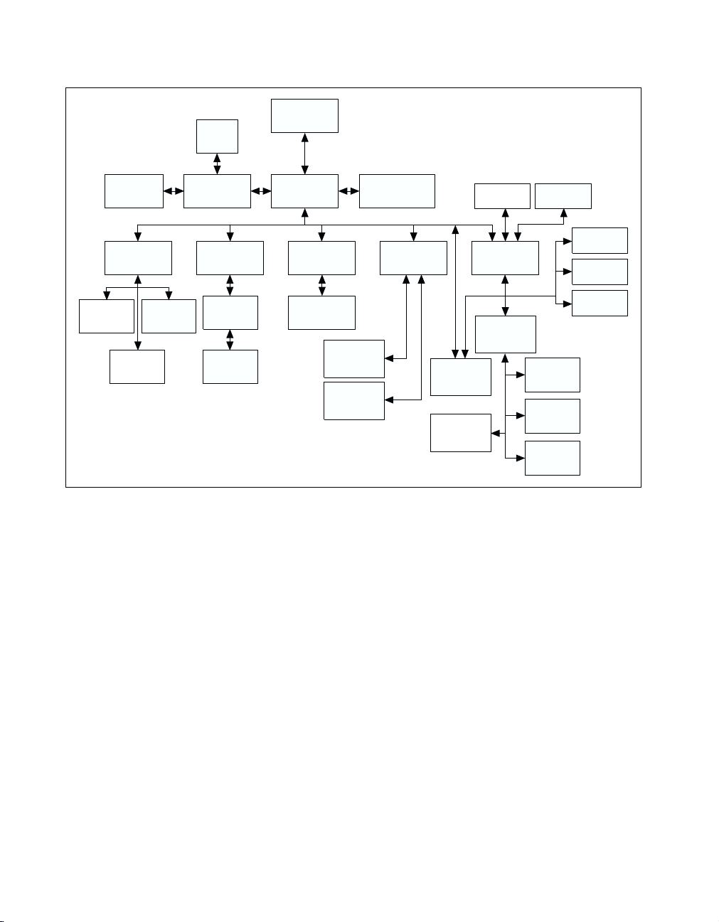
Chapter 5 Functional Overview
2MB
SGRAM
Pentium II
Video
Connector
MITE VXI
Interface
VXI
Interrupts
VXI Bus
Connectors
Processor
VXI
Triggers
AGP Graphics
miniMite
GPIB TNT
GPIB
Connector
PCI Bus
Intel 440BX
PCI PCMCIA
1 Type I/II/III
1 Type I/II
Connectors
SDRAM Sockets
10/100
RJ-45
Connector
SCSI-3
Connector
3 SODIMM
10/100 Enet
SCSI-3
Ultra
DMA33 IDE
Intel PIIX4
ISA Bus
Super IO
PCI/ISA Slot
Floppy Drive
2-USB
Por ts
2-Serial
Connectors
Parallel Port
Connector
PS2
Keyboard/
Mouse
Figure 5-1. VXIpc 870 Series Block Diagram
The VXIpc 870 Series controllers are based on the Intel Pentium II, Slot 1
architecture. The CPU connects to the motherboard through the 100 MHz
GTL+ bus. Because of this modular design, you can easily upgrade your
VXIpc 870 Series controller with a new CPU. As your application needs
expand or change in the future, you can save money by changing the CPU
as compared to purchasing a brand new controller. The VXIpc 870 Series
controllers are based on Pentium II technology, and deliver 512 KB of
level two cache.
Real Time
Clock
BIOS
NI Watch
Dog
Chip Set and SDRAM
The VXIpc 870 Series uses the latest in Intel Chip Set technology—the
Intel 440BX Chip Set. The 440BX connects the Pentium II to the AGP
port, PCI bus, and the SDRAM. The 440BX uses a 100 MHz bus for the
CPU and SDRAM connections to give the highest performance possible.
The VXIpc 870 Series has three SO-DIMM sockets that can support a
VXIpc 870 Series User Manual 5-2 www.ni.com
Page 45

maximum of 192 MB of main memory although as DRAM technology
improves, the maximum amount of RAM supported may increase. The
440BX also connects to SVGA through the AGP port. The PCI bus is then
responsible for connecting the rest of the system.
AGP Graphics
The VXIpc 870 Series uses a S3 VirgeMX AGP-based graphics controller
to connect to SVGA. The AGP graphics controller is coupled to 2 MB of
high-speed 64-bit SGRAM. Using the AGP port for graphics delivers a
higher-speed connection between the CPU and graphics controller,
off-loading traffic from the PCI bus. A few of the resolutions you can use
include:
• 640 × 460 16M colors
• 800 × 600 16M colors
• 1024 × 768 64K colors
• 1280 × 1024 256 colors
• 1600 × 1200 256 colors
10/100 Ethernet and SCSI-3
The Ethernet and SCSI on the VXIpc 870 Series use a Symbios 53C885
dual-function PCI device to connect to 10/100Base Ethernet and Ultra
Wide SCSI-3. The Ethernet function has auto negotiation to connect to
10BaseT and 100BaseTX automatically at 10 Mbits/s and 100 Mbits/s.
The Ultra Wide SCSI-3 function is compatible with SCSI-1, SCSI-2, and
SCSI-3. It supports 16-bit Ultra Wide SCSI transfers up to 40 Mbytes/s and
8-bit Ultra SCSI synchronous transfers at 20 Mbytes/s.
Chapter 5 Functional Overview
PC CARD Expansion
You can add third-party peripheral cards, such as additional serial ports,
through one of the two PC CARD slots on the front panel. The VXIpc 870
Series can accommodate one Type I/II/III PC CARD and one Type I/II PC
CARD simultaneously. The VXIpc 870 Series uses the Cirrus 6730
PCI-PC CARD bridge.
© National Instruments Corporation 5-3 VXIpc 870 Series User Manual
Page 46

Chapter 5 Functional Overview
PCI or ISA Expansion
The VXIpc-872 motherboard can have an expansion slot for either one
full-length PCI expansion card or one 16-bit XT-height ISA bus card. You
can insert either one PCI or one ISA card, but not both at the same time.
Refer to Appendix D, Modifying and Installing I/O Expansion Boards,for
more information on using this expansion slot. The VXIpc-871 module
does not have this expansion slot.
IEEE 488.2/HS488 Interface
The VXIpc 870 Series uses the miniMITE and TNT4882 ASIC
(compatible with the National Instruments PCI-GPIB) to give full GPIB
control of external instruments via a front-panel connector. GPIB control
capability is fully IEEE 488.2 compatible. The GPIB interface on the
VXIpc 870 Series is fully compatible with the National Instruments
industry-standard NI-488.2 driver for a variety of operating systems.
Any software using NI-488.2 will run on the VXIpc 870 Series. Using the
high-speed HS488 protocol, the VXIpc 870 Series can transfer data at up
to 8 Mbytes/s.
PIIX4
The Intel PIIX4 is the bridge between the PCI bus and the ISA bus. It
features the basic PC counter/timers, interrupt controller, and DMA
controllers. It also connects to the USB port and to an Ultra DMA 33 IDE
interface. The Ultra DMA 33 interface is the fastest means to connect an
industry-standard IDE drive to the system.
Super IO
The Super IO block is the interface to standard PC functions, serial ports,
parallel port, floppy drive, and PS2 keyboard and mouse. The serial ports
can communicate at up to 460.8 kbits/s, and the parallel port supports all
modes of EPP and ECP standards.
NI WatchDOG
The NI WatchDOG is a general-purpose counter/timer that you can use to
monitor running applications and reset the embedded controller or assert a
signal should the system lock up. On a WatchDOG timeout, the
WatchDOG can assert any of the following:
• Reset
• VXI trigger line
VXIpc 870 Series User Manual 5-4 www.ni.com
Page 47

• VXI interrupt
• For more advanced features, please contact National Instruments
The NI-VXI/VISA software makes it easy to use NI WatchDOG. The
NI WatchDOG has a 32 kHz reference clock to clock an 8-bit prescaler that
then clocks an 8-bit counter to accommodate timeouts up to 2 seconds.
Real-Time Clock
The VXIpc 870 Series uses a standard Y2K compliant real-time clock with
a user-replaceable battery for backing up the CMOS setting.
BIOS
The VXIpc 870 Series uses a 2 Mb flash device for BIOS code. The BIOS
code is based on the AWARD Modular BIOS. The BIOS code incorporates
the VIDEO BIOS and SCSI BIOS in one device. The BIOS is user
upgradable though a flash update utility.
Programmable Reset Circuitry
The programmable reset circuitry on the VXIpc 870 Series simplifies
software development. You can program the circuitry to reset the PC based
on VXI SYSRESET or reset the VXI bus only using NI-VXI.
Chapter 5 Functional Overview
VXI Voltage Monitor Circuitry
The VXIpc 870 Series has onboard logic to check all VXI backplane
voltages. The PWROK status LED indicates when all voltages are present.
This LED can give you a quick indication that something is wrong with the
system. The voltage monitor can be configured to monitor all VXI power
on just the voltages needed by the VXIpc 870 Series.
Fused Power Protection
The VXIpc 870 Series uses resettable fuses on all voltages except +5 V.
The +5 V power is a user-replaceable fuse accessible through the rear of
the unit.
© National Instruments Corporation 5-5 VXIpc 870 Series User Manual
Page 48

Chapter 5 Functional Overview
VXI Bus
VXI Addressing
The VXIpc 870 Series computers feature the MITE and MANTIS custom
ASICs for accessing the VXI backplane resources. To access VXI memory
or VXI devices, the VXIpc 870 Series uses the multiple-windowing
scheme of the MITE, which makes it possible to access all of VXI address
space. You can configure the VXI address windows to view specific areas
of VXI memory, or you can use NI-VXI/VISA to do this automatically.
The MITE exports a total of eight independent VXI address windows. The
NI-VXI/VISA software driver uses three separate windows—one for VXI
configuration space (A16), one for memory space (A24, A32), and one
for internal use. The remaining five windows are completely user
configurable. You can use one or all five windows; you can also configure
the size and location of the windows. This multiple-windowing scheme
alleviates the performance penalty related to the context switching of one
window that you would constantly have to move between the different
address spaces.
DMA Transfers to and from VXI
The VXIpc 870 Series can perform block-mode transfers using one of the
two on-chip DMA controllers on the MITE. Controlling external VXI
devices often consumes valuable CPU time because the microprocessor
typically shoulders the burden of transferring data to and from devices.
However, MITE-based VXI controllers, such as the VXIpc 870 Series, free
up CPU processing time by moving the burden of block data transfers to
one of the DMA controllers integrated in the MITE. Instead of the
computer microprocessor transferring the data and/or commands, the
NI-VXI/VISA software uses the MITE ASIC to execute the block data
transfers. While the MITE transfers the data, the processor can perform
application-specific tasks, such as data presentation and analysis.
VXI Slot 0 Functionality
The VXIpc 870 Series computers have full VXI Slot 0 capability, including
a MODID register and a CLK10 source, as required by the VXIbus
specification. You can also install the VXIpc 870 Series in another slot and
use it in Non-Slot 0 mode. No matter what your configuration needs, the
VXIpc 870 Series can automatically detect whether it is inserted into Slot 0
and automatically enable or disable the Slot 0 onboard circuitry without
switches and jumpers.
VXIpc 870 Series User Manual 5-6 www.ni.com
Page 49

Chapter 5 Functional Overview
External VXI CLK10 Synchronization
The VXIpc 870 Series computers have an SMB connector on the front
panel for an external clock. Onboard programmable logic can configure the
VXIpc 870 Series to drive its 10 MHz VXI CLK10 signal to this connector
as an output or to use this connector as an input for the 10 MHz VXI
CLK10 signal. In this fashion, you can configure multiple mainframes to
operate off a single 10 MHz system clock. All CLK10 routing features are
controllable through software.
VXI Trigger Lines
The VXIpc 870 Series gives programmers full hardware and software
control over the VXI trigger lines. The VXIpc 870 Series has two SMB
trigger I/O connectors on its front panel for routing any of the TTL trigger
lines between the backplane and external devices. The VXI trigger
interface is based on the advanced MANTIS ASIC developed by National
Instruments. The MANTIS provides the complete VXIpc 870 Series VXI
interface to the outer rows of the P2 backplane connector in a single chip.
The VXIpc 870 Series can respond to all VXI-defined protocols on all P2
TTL and ECL trigger lines at the same time. The MANTIS features an
internal cross-matrix switching system for routing between lines as well
as to and from the front panel and onboard clocks. An internal counter
gives sophisticated counting of events and interrupting on trigger edges and
pulses, as well as generating pulse trains, variable length pulses, and pulse
stretching.
VXI Interrupts
The VXIpc 870 Series can function as an interrupter and an interrupt
handler for any or all of the VXIbus interrupt lines in a VXI mainframe.
The VXIpc 870 Series works with both Release on Acknowledge (ROAK)
and Release on Register Access (RORA) devices. All interrupts are routed
to the microprocessor. The VXIpc 870 Series can also detect other VXIbus
conditions, including assertion of ACFAIL, SYSFAIL, and BERR.
© National Instruments Corporation 5-7 VXIpc 870 Series User Manual
Page 50

BIOS
This chapter contains information on the BIOS (Basic Input Output
System), the low-level interface between the hardware and PC software
that configures and tests your hardware at boot up. The BIOS features an
easy-to-use graphical user interface you use to configure system aspects
according to your needs.
Entering BIOS Setup
To enter the BIOS setup program, perform the following steps:
1. Turn on or reboot the system. A screen appears with a series of
diagnostic checks.
2. When
press the <DEL> key to enter the BIOS setup program.
3. Choose options with the keyboard. Modify the settings to reflect
system options.
Hit <DEL> if you want to run SETUP
6
appears,
Default BIOS Setup Settings
To restore the default settings while inside the BIOS setup program,
select either FAILSAFE Defaults or OPTIMAL Defaults.
Select the Optimal settings if you want to get maximum performance from
the VXIpc 870 Series. Fail Safe settings are for debugging purposes.
© National Instruments Corporation 6-1 VXIpc 870 Series User Manual
Page 51

Specifications
This appendix lists the specifications for the VXIpc 870 Series embedded
computer.
Requirements
VXIbus configuration space................... 64 KB
A24 or A32 space................................... programmable
Minimum ........................................ 16 KB
Environmental
Temperature
Operating ........................................ 0 to 50 °C
Storage ............................................ –20 to 70 °C
Relative humidity
Operating ........................................ 10 to 90% noncondensing
Storage ............................................ 5 to 95% noncondensing
A
EMI ........................................................ FCC Class A verified, EC verified
Random vibration
Operational......................................5 to 500 Hz, 0.3 g
Non-operational .............................. 5 to 500 Hz, 2.4 g
Functional shock .................................... MIL-T-28800E Class 3
(per Section 4.5.5.4.1)
Half-sine shock pulse
(11 ms duration, 30 g peak,
3 shocks per face).
Also meets IEC standard
60068-2-27.
© National Instruments Corporation A-1 VXIpc 870 Series User Manual
RMS
RMS
, 3 axes
, 3 axes
Page 52

Appendix A Specifications
Power Requirement
+5 V is fused with a user-replaceable glass fuse, type 3AG, 15A, Slowblow.
All other voltages use a resettable-type circuit protector that requires no
replacement by the user.
+5 V
Typical.............................................8 A
Maximum ........................................15 A
–5.2 V
Typical.............................................224.5 mA
Maximum ........................................2 A
–2V
Typical.............................................67.2 mA
Maximum ........................................2 A
+12 V
Typical.............................................102.6 mA
Maximum ........................................2 A
Physical
–12 V
Typical.............................................2.43 mA
Maximum ........................................2 A
+24 V
Typical.............................................1 mA
-24 V
Typical.............................................1 mA
Dimensions
Fully enclosed, shielded VXI C-size module
233.35 by 340 mm (9.187 by 13.386 in.)
Weight
With 64 MB DRAM Installed .........2.5 Kg (5.51 lb.)
Slot requirements....................................Two VXI C-size slots
VXIpc 870 Series User Manual A-2 www.ni.com
Page 53

Compatibility ......................................... Fully compatible with
VXI keying class.................................... Class 1 TTL
MTBF..................................................... TBD
VMEbus Capability Codes
A32, A24, A16 (master)
VMEbus master A32, A24, and A16 addressing
A32, A24, A16 (slave)
VMEbus slave A32, A24, and A16 addressing
D64, D32, D16, D08(EO) (master)
VMEbus master D64, D32, D16, and D08 data sizes
D64, D32, D16, D08(EO) (slave)
VMEbus slave D64, D32, D16, and D08 data sizes
BLT, MBLT (master)
VMEbus master block and D64 transfers
Appendix A Specifications
VXI specification
BLT, MBLT (slave)
VMEbus slave block and D64 transfers
RMW (master)
VMEbus master read/modify/write transfers
RMW (slave)
VMEbus slave read/modify/write transfers
RETRY (master)
VMEbus master retry support
RETRY (slave)
VMEbus slave retry support
FSD
First slot detector
SCON
VMEbus System Controller (Automatic Detection)
© National Instruments Corporation A-3 VXIpc 870 Series User Manual
Page 54

Appendix A Specifications
PRI, RRS
Prioritized or Round Robin Select arbiter
ROR, RWD, FAIR
Release on Request, Release When Done, and FAIR bus requester
IH(7–1)
Interrupt handler for levels 7–1
I(7–1)
Interrupt requester for levels 7–1
D32, D16, D08(O) (Interrupt Handler)
VMEbus D32, D16, D08(O) interrupt handler
D32, D16, D08(O) (Interrupter)
VMEbus D32, D16, D08(O) interrupter
ROAK, RORA
Release on Acknowledge or Register Access interrupter
BTO(
)
x
VMEbus bus timer (programmable limit)
LOCK
Can lock the VMEbus for indivisible transfers
VXIpc 870 Series User Manual A-4 www.ni.com
Page 55

LED Indicators
This appendix describes how to read the LEDs on the front panel to
interpret the status of the VXIpc 870 Series.
VXIbus Interface Status LEDs
The VXIbus interface status LEDs are located at the top of the module
and include four LEDs: FAIL, SYSF, ONLINE,andPWROK.
They indicate the various stages of initialization that occur as the
VXIpc 870 Series boots. The following paragraphs describe each LED.
SYSF LED
The SYSF LED is lit when the VXIbus SYSFAIL signal is asserted. It does
not necessarily indicate that the VXIpc 870 Series is asserting SYSFAIL,
only that there is a device in the system asserting SYSFAIL.
FAIL LED
The FAIL LED is lit when the VXIpc 870 Series is driving the SYSFAIL
signal. The VXIpc 870 Series asserts SYSFAIL when the PASSED bit in its
VXIbus status register is clear. The PASSED bit is set by the power-on self
configuration circuitry (POSC) when it has completed initializing the
VXIbus interface.
B
ONLINE LED
The ONLINE LED is lit when the Resource Manager has successfully
completed and the VXIbus interface is ready for application programs.
PWROK LED
The PWROK LED is lit when all the various voltages on the VXIbus
backplane are present and within the tolerance range of the onboard
detection circuitry. These voltages are monitored behind short circuit
protection devices. If the PWROK LED is not lit, it could indicate either
that a fuse is blown or one of the VXIbus power supplies is not working.
© National Instruments Corporation B-1 VXIpc 870 Series User Manual
Page 56

Appendix B LED Indicators
LEDs and System Startup Cycle
Table B-1 shows a system startup cycle and possible points of failure, up to
and including the state in which the ONLINE LED is asserted.
Table B-1. LEDs and System Startup Status
Possible Problem if
Step LEDs Lit Status
1 None Machine just turned on. The VXIpc 870 Series is not
receiving power or a fuse is blown.
PWROK
2
Machine just turned on. The VXIpc 870 Series is now
starting to boot. All voltages are
present.
PWROK,
3
FAIL,
SYSF
Now asserting FAIL because
VXIbus interface has not been
initialized yet.
Power-on self configuration
(POSC) cannot execute because
of problems with system reset or
because the POSCEN switch is
incorrectly configured.
PWROK
4
POSC cycles are complete. VXI port
isreadytorespondtoResource
Manager inquiries.
POSC completed successfully;
however, the Resource Manager
either hung or was not executed.
VXIpc 870 Fails
PWROK,
5
Online
Resource Manager has been
executed, indicating that the VXI
Resource Manager interface
initialized successfully.
software can now communicate with
the VXIbus circuitry.
If either the SYSF or FAIL LED remains lit, perform the following steps:
1. Power off the mainframe.
2. Remove all other modules from the mainframe.
3. Make sure that the VXIpc 870 Series switch and jumper settings are
correct.
4. Make sure that the VXIpc 870 Series is seated properly in the
mainframe.
5. Power on the mainframe and observe whether the SYSF and FAIL
LEDs become unlit some time before the operating system boots.
VXIpc 870 Series User Manual B-2 www.ni.com
Page 57

Board Access LEDs
The board access LEDs—ACC, DRV,andSCSI—indicate when
board resources have been accessed. The following paragraphs describe
these LEDs.
ACC LED
When lit, the ACC LED indicates that the VXIpc 870 Series MODID line
is asserted or that another VXIbus master is accessing VXIbus shared
registers or shared memory.
DRV LED
The DRV LED light indicates that an access to the internal hard disk drive
or the CD-ROM on the 871 is occurring.
SCSI LED
The SCSI LED light indicates that an access to an external hard disk drive
is occurring.
Appendix B LED Indicators
Ethernet LEDs
The Ethernet LEDs (RX/TX, LNK,and100B-T) indicate the status of the
Ethernet interface on the VXIpc 870 Series.
RX/TX LED
The RX/TX LED lights when the Ethernet interface is receiving or
transmitting a packet.
LNK LED
The LNK LED indicates link status—in this case, that the controller is
connected to a valid Ethernet port.
100B-T
The 100B-T LED indicates that the current Ethernet connection is at
100 Mbits/s when lit.
© National Instruments Corporation B-3 VXIpc 870 Series User Manual
Page 58

Front Panel and Connectors
This appendix describes the front panel and connectors on the VXIpc 870
Series. This material contains the information relevant to VXIplug&play
Specification VPP-8, VXI Module/Mainframe to Receiver Interconnection.
Note
The illustrations in this appendix show the mating face of the connectors.
An asterisk (*) after a signal name indicates that the signal is active low.
The VXIpc 870 Series has the following front panel connectors:
• TwoRS-232Serial
• Extended Capabilities Parallel (ECP)
• SVGA Controller
• IEEE 488.2
• 10/100 Ethernet
• UW-SCSI
• External Clock
• Trigger Output
• Trigger Input
• Audio Output
• PS/2-Style Keyboard
• PS/2-Style Mouse
• Two U SB
C
This appendix also describes the VXIbus connector on the VXIpc 870
Series, which connects to the backplane of the VXIbus mainframe.
© National Instruments Corporation C-1 VXIpc 870 Series User Manual
Page 59
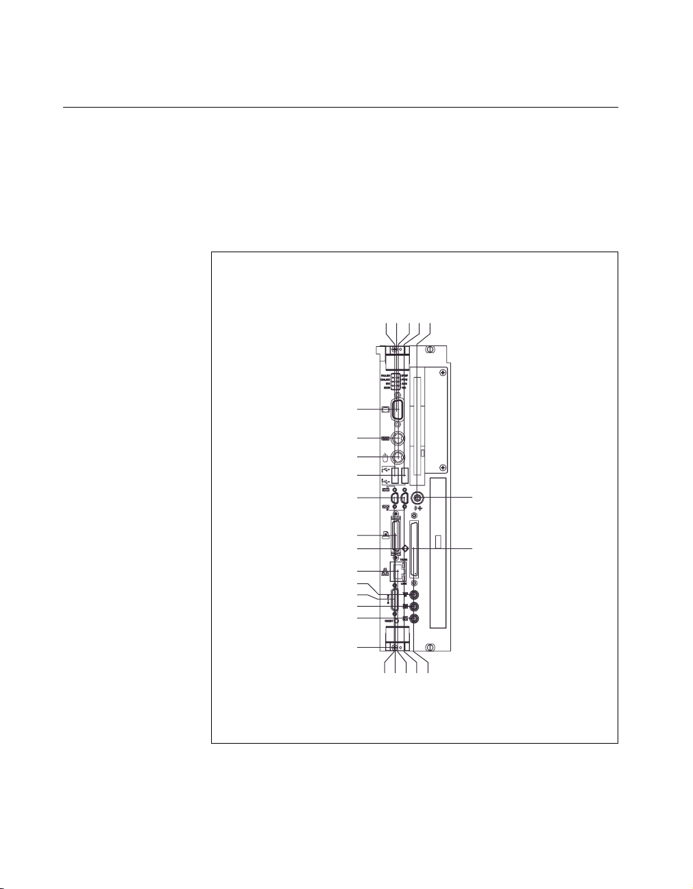
Appendix C Front Panel and Connectors
Front Panel
Figure C-1 shows the front panel layout of the VXIpc-871, Figure C-2
shows the layout of the VXIpc-872, and Figures C-3 and C-4 show the
layouts of the VXIpc-873 with nonremovable and removable flash drives,
respectively. The drawings show dimensions relevant to key elements on
the front panel. Dimensions are shown in inches and millimeters, with
millimeter dimensions in square brackets. The front panel thickness for
all models in the VXIpc 870 Series is 2.49 mm (0.098 in.).
8.034 [204.06]
7.064 [179.41]
6.424 [163.16]
5.805 [147.44]
5.045 [128.14]
3.776 [95.91]
3.322 [84.38]
2.564 [65.13]
1.779 [45.19]
1.620 [41.14]
1.379 [35.03]
0.979 [24.87]
0.000 [0.00]
0.023 [0.58]
0.102 [2.59]
0.111 [2.82]
0.342 [8.70]
0.770 [19.56]
5.052 [128.32]
3.320 [84.32]
0.003 [0.08]
0.120 [3.05]
0.338 [8.59]
0.041 [1.04]
0.660 [16.76]
Figure C-1. VXIpc-871 Front Panel Layout and Dimensions
VXIpc 870 Series User Manual C-2 www.ni.com
Page 60
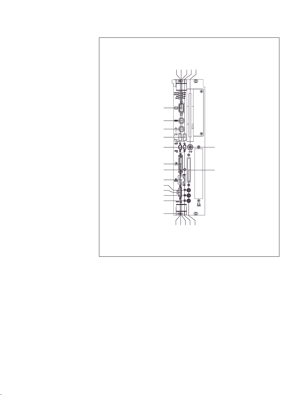
Appendix C Front Panel and Connectors
8.034 [204.06]
7.064 [179.41]
6.424 [163.16]
5.805 [147.44]
5.045 [128.14]
3.776 [95.91]
3.322 [84.38]
2.564 [65.13]
1.779 [45.19]
1.620 [41.14]
1.379 [35.03]
0.979 [24.87]
0.000 [0.00]
0.023 [0.58]
0.102 [2.59]
0.111 [2.82]
0.342 [8.70]
0.770 [19.56]
5.052 [128.32]
3.320 [84.32]
0.003 [0.08]
0.120 [3.05]
0.338 [8.59]
0.041 [1.04]
0.660 [16.76]
Figure C-2. VXIpc-872 Front Panel Layout and Dimensions
© National Instruments Corporation C-3 VXIpc 870 Series User Manual
Page 61
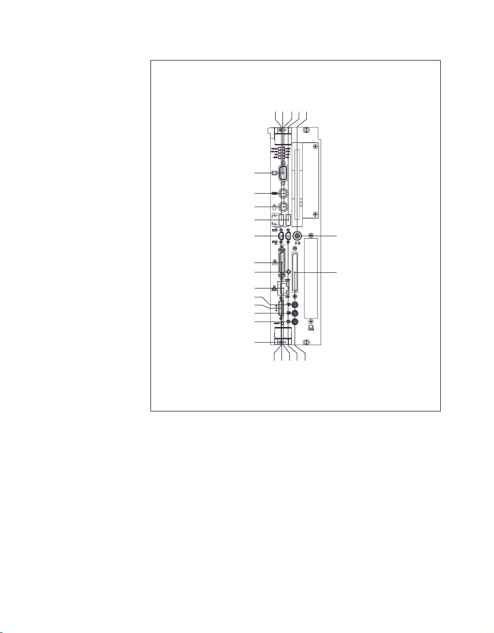
Appendix C Front Panel and Connectors
8.034 [204.06]
7.064 [179.41]
6.424 [163.16]
5.805 [147.44]
5.045 [128.14]
3.776 [95.91]
3.322 [84.38]
2.564 [65.13]
1.779 [45.19]
1.620 [41.14]
1.379 [35.03]
0.979 [24.87]
0.000 [0.00]
0.023 [0.58]
0.102 [2.59]
0.111 [2.82]
0.342 [8.70]
0.770 [19.56]
5.052 [128.32]
3.320 [84.32]
0.003 [0.08]
0.120 [3.05]
0.338 [8.59]
0.041 [1.04]
0.660 [16.76]
Figure C-3. VXIpc-873 Front Panel Layout and Dimensions
(Option 1 with Internal, Nonremovable Flash Drive)
VXIpc 870 Series User Manual C-4 www.ni.com
Page 62
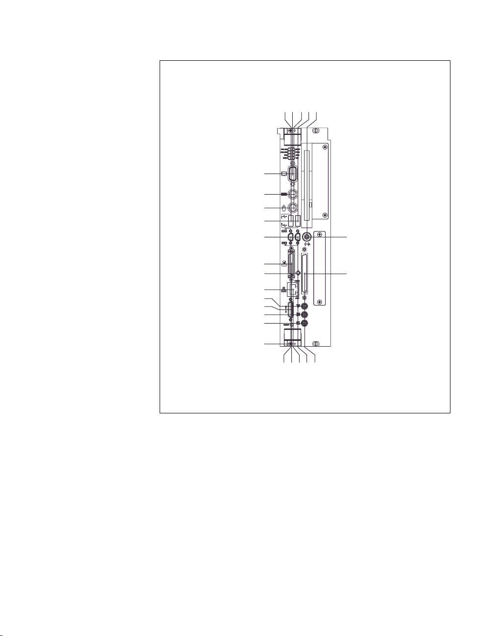
Appendix C Front Panel and Connectors
8.034 [204.06]
7.064 [179.41]
6.424 [163.16]
5.805 [147.44]
5.045 [128.14]
3.776 [95.91]
3.322 [84.38]
2.564 [65.13]
1.779 [45.19]
1.620 [41.14]
1.379 [35.03]
0.979 [24.87]
0.000 [0.00]
0.023 [0.58]
0.102 [2.59]
0.111 [2.82]
0.342 [8.70]
0.770 [19.56]
5.052 [128.32]
3.320 [84.32]
0.003 [0.08]
0.120 [3.05]
0.338 [8.59]
0.041 [1.04]
0.660 [16.76]
Figure C-4. VXIpc-873 Front Panel Layout and Dimensions
(Option 2 with Removable Flash Drive)
© National Instruments Corporation C-5 VXIpc 870 Series User Manual
Page 63
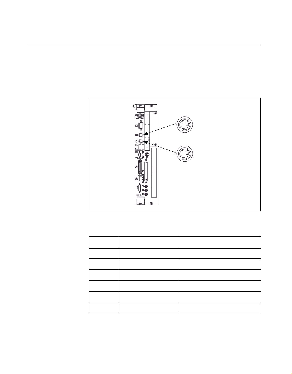
Appendix C Front Panel and Connectors
Keyboard and Mouse
Figure C-5 shows the location and pinouts for the keyboard and mouse
connectors on the VXIpc 870 Series. Table C-1 gives the name and
description for the keyboard and mouse connector signals.
Amp manufactures a mating connector with part numbers 212437-4
(housing), 212435-7 (ferrule), and 66735-4 (pin contact).
4
6
2
1
2
1
Keyboard
5
3
4
6
Mouse
5
3
Figure C-5. Keyboard and Mouse Connectors Location and Pinout
Table C-1. Keyboard and Mouse Connector Signals
Pin Signal Name Signal Description
1 DATA Data
2 NC Not Connected
3 GND Ground
4 +5V +5 Volts
5 CLK Clock
6 NC Not Connected
VXIpc 870 Series User Manual C-6 www.ni.com
Page 64
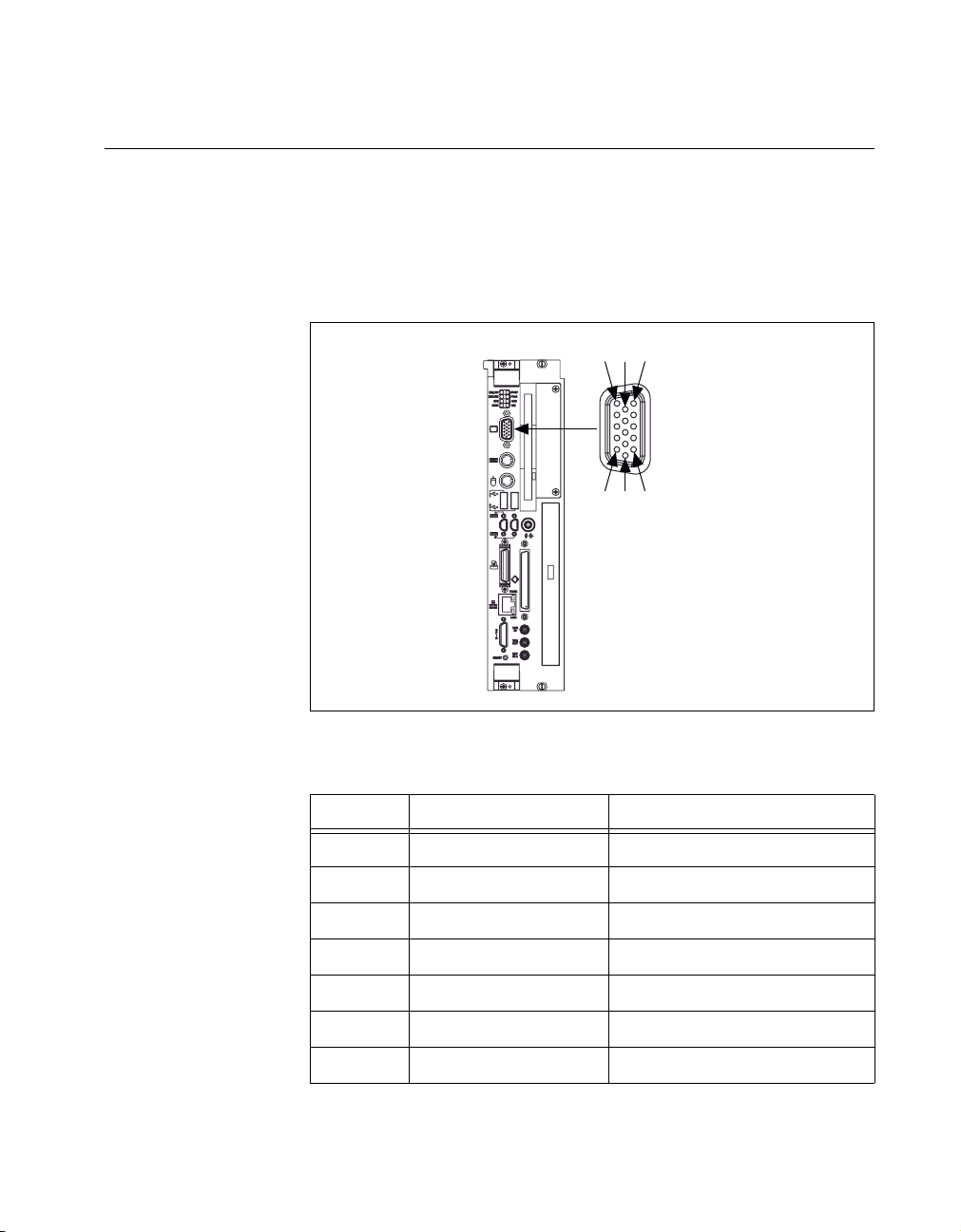
SVGA
Appendix C Front Panel and Connectors
Figure C-6 shows the location and pinouts for the SVGA connector on the
VXIpc 870 Series. Table C-2 gives the name and description for the SVGA
connector signals.
Amp manufactures a mating connector with part numbers 748364-1
(housing) and 748333-2 (pin contact).
51015
SVGA
1611
Figure C-6. SVGA Connector Location and Pinout
Table C-2. SVGA Connector Signals
Pin Signal Name Signal Description
1 R Red
2 G Green
3 B Blue
4 NC Not Connected
5 GND Ground
6 GND Ground
7 GND Ground
© National Instruments Corporation C-7 VXIpc 870 Series User Manual
Page 65
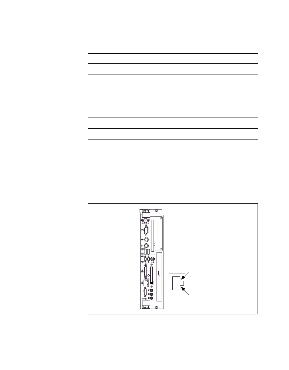
Appendix C Front Panel and Connectors
Pin Signal Name Signal Description
10 GND Ground
11 NC Not Connected
12 SD Serial Data
13 HSync Horizontal Sync
14 VSync Ve r t i c al S y n c
15 SC Serial Clock
Ethernet
Figure C-7 shows the location and pinouts for the Ethernet connector
on the VXIpc 870 Series Table C-3 gives the name and description for the
Ethernet connector signals.
Table C-2. SVGA Connector Signals (Continued)
8 GND Ground
9 NC Not Connected
Amp manufactures a mating connector, part number 554739-1.
1
Ethernet
8
Figure C-7. Ethernet Connector Location and Pinout
VXIpc 870 Series User Manual C-8 www.ni.com
.
Page 66
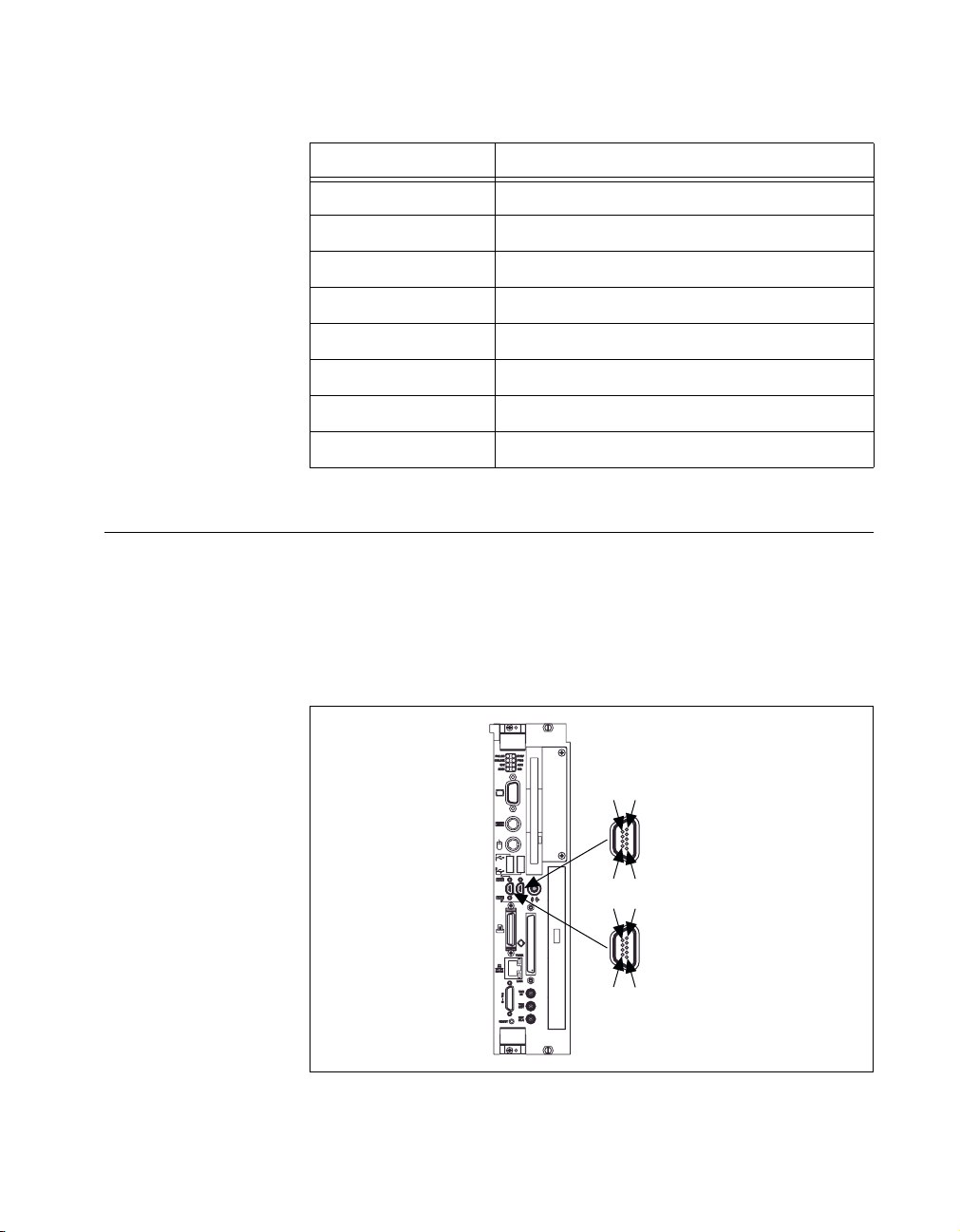
Appendix C Front Panel and Connectors
COM1 and COM2
Figure C-8 shows the location and pinouts for the COM1 and COM2
connectors on the VXIpc 870 Series. Table C-4 gives the name and
description for the COM1 and COM2 connector signals.
ITT Cannon manufactures a serial port mating connector, part number
MDSM-9SC-Z11, for the COM1 and COM2 connectors.
Table C-3.
Ethernet Connector Signals
Pin Signal Description
1 Differential Transmit +
2 Differential Transmit –
3 Differential Receive +
4 Not Connected
5 Not Connected
6 Differential Receive –
7 Not Connected
8 Not Connected
61
COM1
95
61
COM2
95
Figure C-8. COM1 and COM2 Connectors Location and Pinout
© National Instruments Corporation C-9 VXIpc 870 Series User Manual
.
Page 67
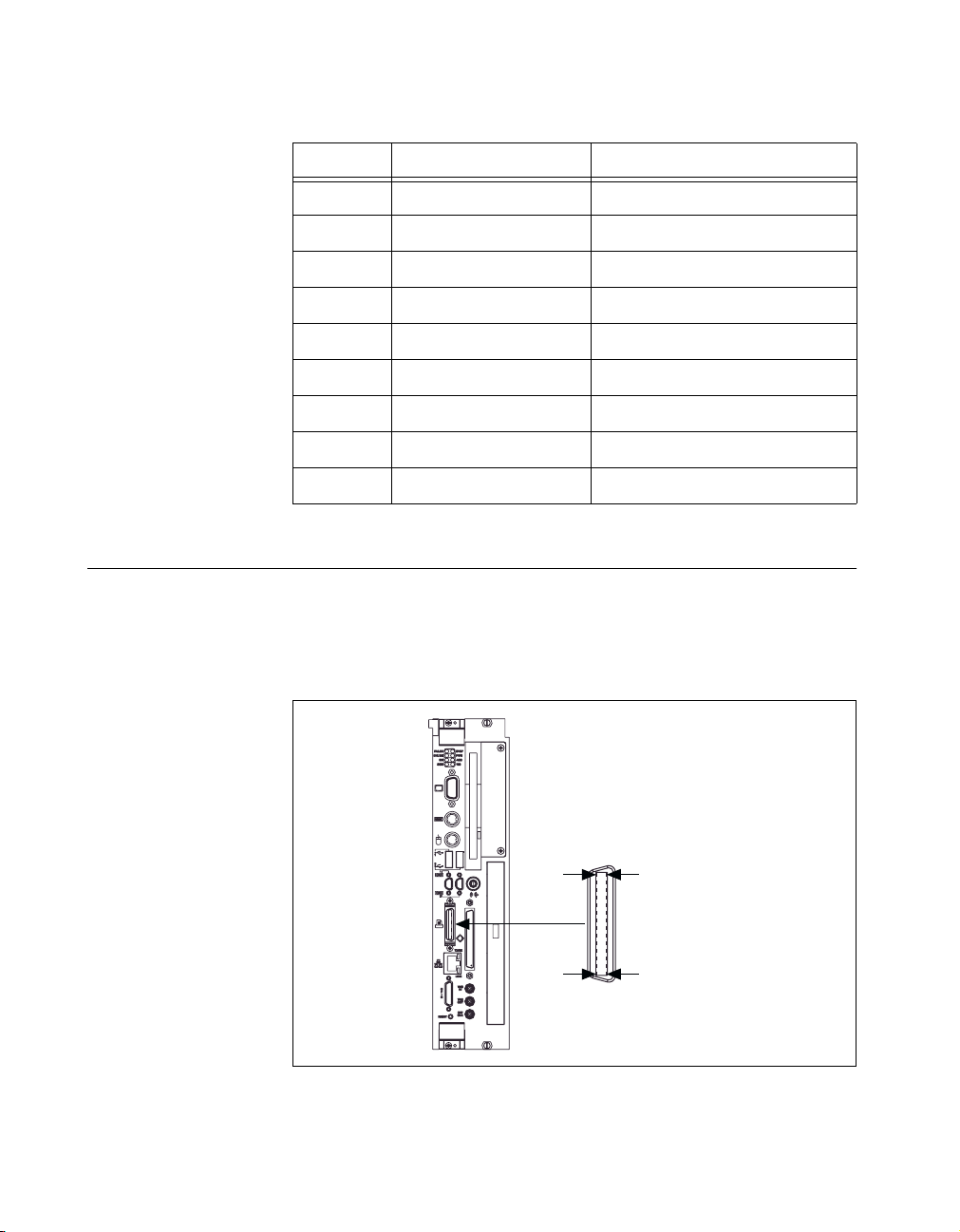
Appendix C Front Panel and Connectors
Pin Signal Name Signal Description
Parallel Port
Figure C-9 shows the location and pinouts for the IEEE-1284 connector on
the VXIpc 870 Series. Table C-5 gives the name and description for the
IEEE-1284 connector signals.Amp manufactures a parallel port compatible
connector, part number 2-175677-5.
Table C-4. COM1 and COM2 Connector Signals
1 DCD* Data Carrier Detect
2 RXD* Receive Data
3 TXD* Transmit Data
4 DTR* Data Terminal Ready
5 GND Ground
6 DSR* Data Set Ready
7 RTS * Ready to Send
8 CTS* Clear to Send
9 RI* Ring Indicator
36
19
Figure C-9. Parallel Port Connector Location and Pinout
VXIpc 870 Series User Manual C-10 www.ni.com
18
Parallel Port
1
Page 68

Appendix C Front Panel and Connectors
Table C-5.
Parallel Port Connector Signals
Pin Signal Name Signal Description
1 BUSY* Device Busy
2 SLCTIN* Select Input
3 ACK* Acknowledge
4 FAULT* Fault
5 ERROR Error
6 PD0 Data Bit 0
7 PD1 Data Bit 1
8 PD 2 Data Bit 2
9 PD3 Data Bit 3
10 PD4 Data Bit 4
11 PD5 Data Bit 5
12 PD6 Data Bit 6
13 PD7 Data Bit 7
14 INIT* Initialize Printer
15 STROBE* Strobe
16 SLCT Select
17 AUTO FD Auto Line Feed
18 +5V +5 V
19–35 GND Ground
36 NC Not Connected
© National Instruments Corporation C-11 VXIpc 870 Series User Manual
Page 69
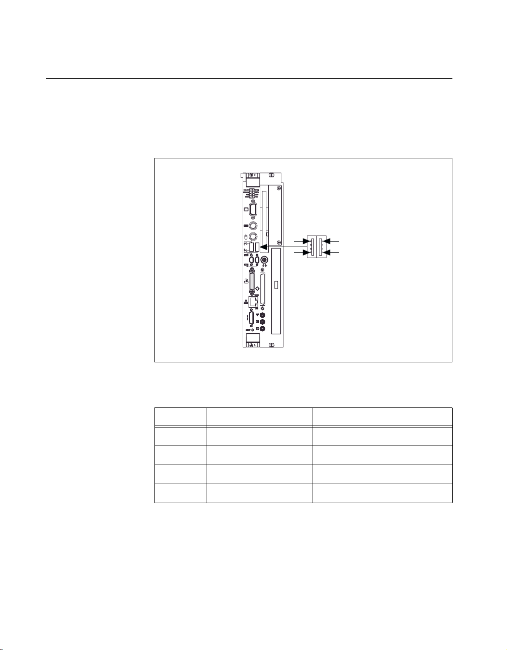
Appendix C Front Panel and Connectors
Universal Serial Bus
Figure C-10 shows the location and pinouts for the two Universal Serial
Bus (USB) connectors on the VXIpc 870 Series. Table C-6 gives the name
and description for the USB connector signals.
Amp manufactures a mating connector, part number 787633.
1
4
Figure C-10. USB Connectors Location and Pinout
Table C-6. USB Connector Signals
1
USB
4
Pin Signal Name Signal Description
1 VCC Cable Power (+5 V)
2 –Data USB Data–
3 +Data USB Data+
4 GND Ground
VXIpc 870 Series User Manual C-12 www.ni.com
Page 70
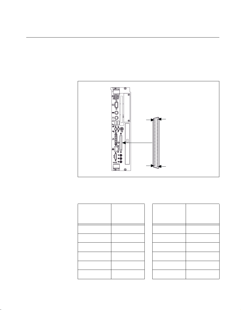
SCSI
Appendix C Front Panel and Connectors
Figure C-11 shows the location and pinouts for the Ultra Wide SCSI
connector on the VXIpc 870 Series. Table C-7 gives the name and
description for the SCSI connector signals.
Amp manufactures a SCSI compatible connector, part number 749111-6,
with shielded enclosure 750752-1.
68
35
Figure C-11. SCSI Connector Location and Pinout
Table C-7. 16-Bit Wide SCSI-3 “P” (Primary) Connector Pinout
(Single Ended)
High Density
34
Ultra-wide
SCSI
1
High Density
68-Pin
SCSI Signal
Connector
SCSI Signal
GND 1 DB(12)* 35
GND 2 DB(13)* 36
GND 3 DB(14)* 37
GND 4 DB(15)* 38
68-Pin
Connector
GND 5 DP1 39
GND 6 DB(0)* 40
© National Instruments Corporation C-13 VXIpc 870 Series User Manual
Page 71

Appendix C Front Panel and Connectors
Table C-7. 16-Bit Wide SCSI-3 “P” (Primary) Connector Pinout
(Single Ended) (Continued)
High Density
68-Pin
SCSI Signal
Connector
SCSI Signal
GND 7 DB(1)* 41
GND 8 DB(2)* 42
GND 9 DB(3)* 43
GND 10 DB(4)* 44
GND 11 DB(5)* 45
GND 12 DB(6)* 46
GND 13 DB(7)* 47
GND 14 DP0 48
GND 15 GND 49
GND 16 GND 50
TERMPWR 17 TERMPWR 51
TERMPWR 18 TERMPWR 52
RSRVD 19 RSRVD 53
GND 20 GND 54
High Density
68-Pin
Connector
GND 21 AT N * 55
GND 22 GND 56
GND 23 BSY* 57
GND 24 ACK* 58
GND 25 RST* 59
GND 26 MSG* 60
GND 27 SEL* 61
GND 28 C/D* 62
GND 29 REQ* 63
GND 30 I/O* 64
VXIpc 870 Series User Manual C-14 www.ni.com
Page 72
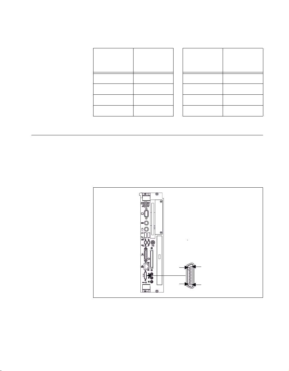
Appendix C Front Panel and Connectors
Table C-7. 16-Bit Wide SCSI-3 “P” (Primary) Connector Pinout
(Single Ended) (Continued)
SCSI Signal
GND 31 DB(8)* 65
GND 32 DB(9)* 66
GND 33 DB(10)* 67
GND 34 DB(11)* 68
GPIB (IEEE-488.2)
Figure C-12 shows the location and pinouts for the GPIB connector on the
VXIpc 870 Series. Table C-8 gives the name and description for the GPIB
connector signals.
ITT Cannon manufactures a GPIB mating connector, part number
MDSM-255C-Z11.
High Density
68-Pin
Connector
SCSI Signal
High Density
68-Pin
Connector
14
25
Figure C-12.
© National Instruments Corporation C-15 VXIpc 870 Series User Manual
GPIB Connector Location and Pinout
1
GPIB
13
Page 73

Appendix C Front Panel and Connectors
Pin Signal Name Signal Description
10 SRQ* Service Request
11 AT N * Attention
12 SHIELD Chassis ground
Table C-8. GPIB Connector Signals
1 DIO1* Data Bit 1
2 DIO2* Data Bit 2
3 DIO3* Data Bit 3
4 DIO4* Data Bit 4
5 EOI* End or Identify
6 DAV* Data Valid
7 NRFD* Not Ready for Data
8 NDAC* Not Data Accepted
9 IFC* Interface Clear
13 DIO5* Data Bit 5
14 DIO6* Data Bit 6
15 DIO7* Data Bit 7
16 DIO8* Data Bit 8
17 REN* Remote Enable
18–25 GND Logic Ground
VXIpc 870 Series User Manual C-16 www.ni.com
Page 74
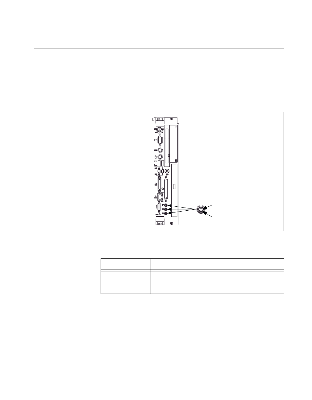
External SMBs
Appendix C Front Panel and Connectors
Figure C-13 shows the location and pinouts for the SMB connectors on the
VXIpc 870 Series. The SMB connectors are used for an external clock
signal and TTL trigger input and output. Table C-9 gives the name and
description for the SMB connector signals. Also see Table C-10 for a
description of the signal characteristics for the SMB connections.
Amp manufactures an SMB mating connector, part number 1-413985-0.
Center
SMB
Shield
Figure C-13.
SMB Connectors Location and Pinout
Table C-9. SMB Connector Signals
Pin Signal Description
Center TTL Trigger or Clock Signal
Shield Ground
© National Instruments Corporation C-17 VXIpc 870 Series User Manual
Page 75
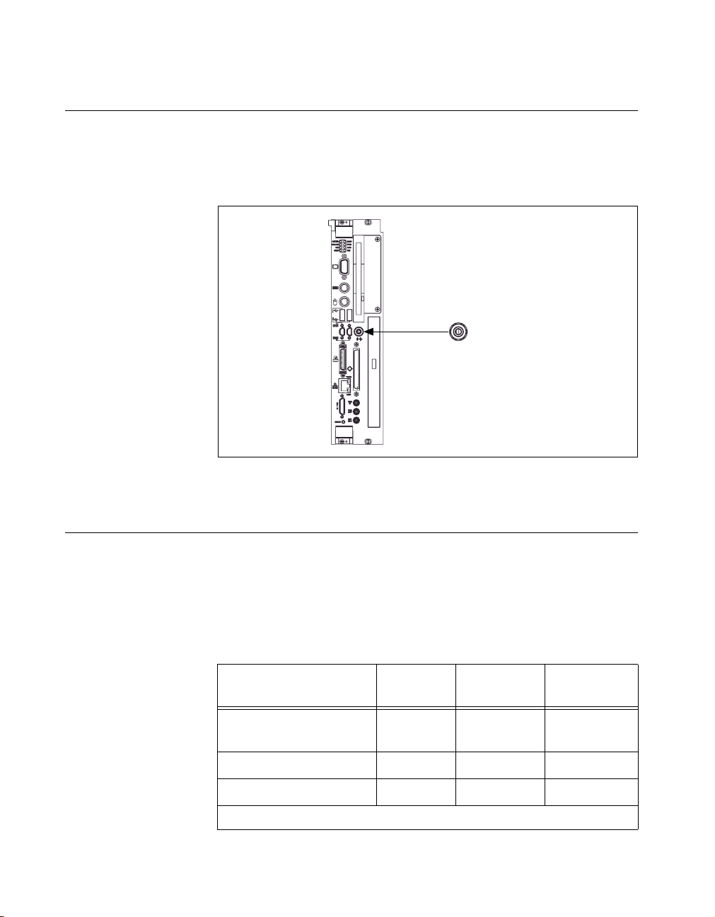
Appendix C Front Panel and Connectors
Speaker
Figure C-14 shows the location of the speaker connection on the
VXIpc 870 Series.
Switchcraft manufactures a mating speaker connector, part number 750.
Speaker
Figure C-14. Speaker Connection Location
Signal Characteristics
Refer to the relevant standard for the signal characteristics for VGA, SCSI,
Ethernet, keyboard, mouse, parallel, serial, and GPIB.
Table C-10 shows the signal characteristics for the SMB and speaker
connections.
Table C-10. Signal Characteristics for SMB and Speaker Connections
Voltage
Signal
SMB
(TRIG out, CLK out)
SMB (TRIG in) 0to5V 100 mA* DC-10 MHz
Speaker 0to4.3V 75 mA DC-20 kHz
*With50Ω termination
VXIpc 870 Series User Manual C-18 www.ni.com
Range
0to3.4V 200 mA DC-10 MHz
Maximum
Current
Frequency
Range
Page 76
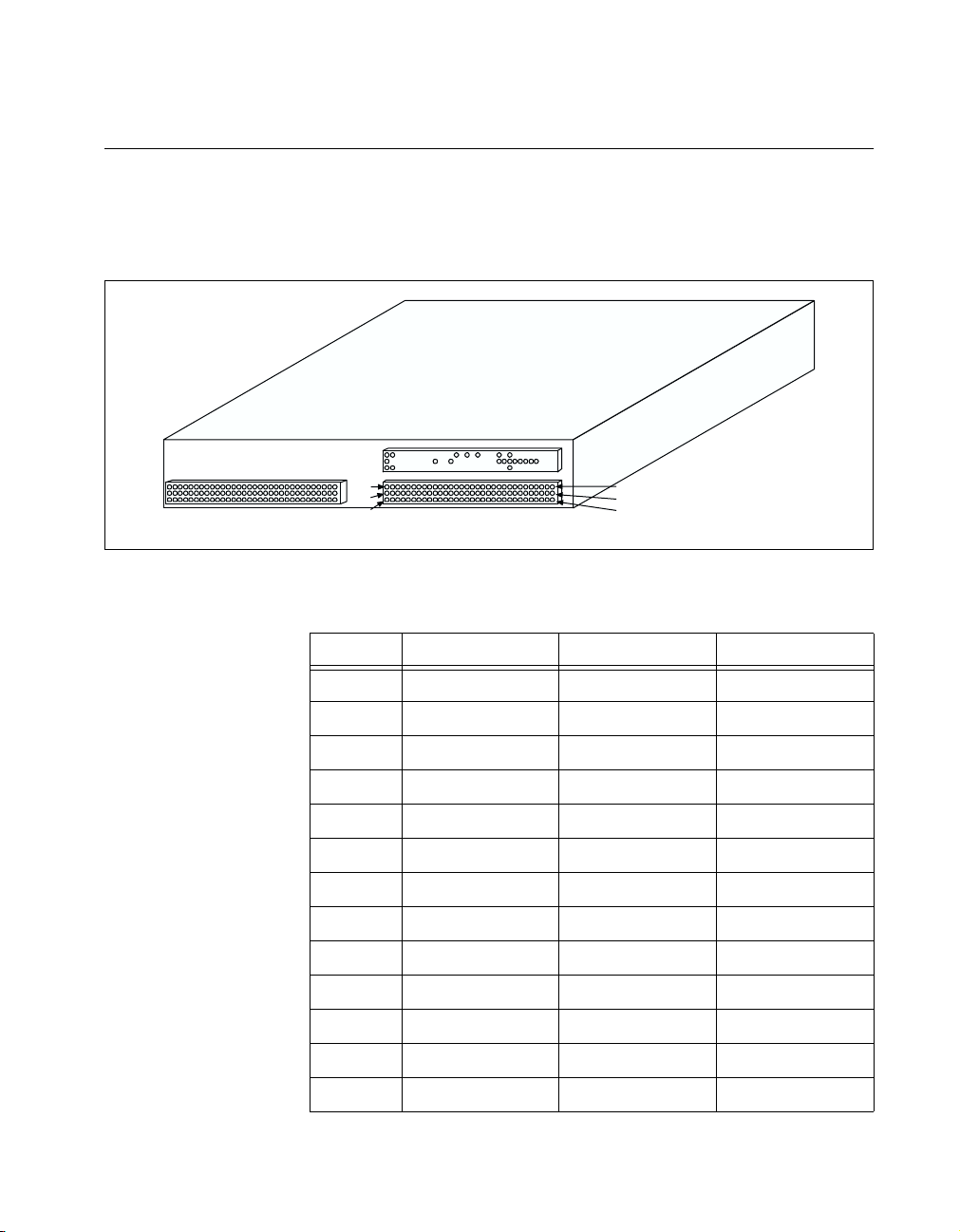
VXIbus P1 and P2
Figure C-15 shows the location and pinouts for the VXIbus connector on
the VXIpc 870 Series. Table C-11 gives the name and description for the
VXIbus P1 connector signals. Table C-12 gives the name and description
for the VXIbus P2 connector signals.
Appendix C Front Panel and Connectors
C32
B32
A32
P1 ConnectorP2 Connector
Figure C-15. VXIbus Connectors Location and Pinout
Table C-11.
VXIbus P1 Connector Signals
C1
B1
A1
Pin Row C Row B Row A
1 D08 BBSY* D00
2 D09 BCLR* D01
3 D10 ACFAIL* D02
4 D11 BG0IN* D03
5 D12 BG0OUT* D04
6 D13 BG1IN* D05
7 D14 BG1OUT* D06
8 D15 BG2IN* D07
9 GND BG2OUT* GND
10 SYSFAIL* BG3IN* SYSCLK
11 BERR* BG3OUT* GND
12 SYSRESET* BR0* DS1*
13 LWORD* BR1* DS0*
© National Instruments Corporation C-19 VXIpc 870 Series User Manual
Page 77

Appendix C Front Panel and Connectors
Pin Row C Row B Row A
14 AM5 BR2* WRITE*
15 A23 BR3* GND
16 A22 AM0 DTACK*
17 A21 AM1 GND
18 A20 AM2 AS*
19 A19 AM3 GND
20 A18 GND IACK*
21 A17 Not Connected IACKIN*
22 A16 Not Connected IACKOUT*
23 A15 GND AM4
24 A14 IRQ7* A07
25 A13 IRQ6* A06
26 A12 IRQ5 A05
Table C-11. VXIbus P1 Connector Signals (Continued)
27 A11 IRQ4 A04
28 A10 IRQ3 A03
29 A09 IRQ2 A02
30 A08 IRQ1 A01
31 +12 V Not Connected –12 V
32 +5 V +5 V +5 V
Table C-12. VXIbus P2 Connector Signals
Pin Row C Row B Row A
1 CLK10+ +5 V ECLTRG0
2 CLK10– GND –2V
3 GND Not Connected ECLTRG1
4 –5.2 V A24 GND
5 Not Connected A25 MODID12
VXIpc 870 Series User Manual C-20 www.ni.com
Page 78

Appendix C Front Panel and Connectors
Table C-12. VXIbus P2 Connector Signals (Continued)
Pin Row C Row B Row A
6 Not Connected A26 MODID11
7 GND A27 –5.2 V
8 Not Connected A28 MODID10
9 Not Connected A29 MODID09
10 GND A30 GND
11 Not Connected A31 MODID08
12 Not Connected GND MODID07
13 –2V +5 V –5.2 V
14 Not Connected D16 MODID06
15 Not Connected D17 MODID05
16 GND D18 GND
17 Not Connected D19 MODID04
18 Not Connected D20 MODID03
19 –5.2 V D21 –5.2 V
20 Not Connected D22 MODID02
21 Not Connected D23 MODID01
22 GND GND GND
23 TTLTRG1* D24 TTLTRG0*
24 TTLTRG3* D25 TTLTRG2*
25 GND D26 +5 V
26 TTLTRG5* D27 TTLTRG4*
27 TTLTRG7* D28 TTLTRG6*
28 GND D29 GND
29 Not Connected D30 Not Connected
30 GND D31 MODID00
31 Not Connected GND GND
32 Not Connected +5 V Not Connected
© National Instruments Corporation C-21 VXIpc 870 Series User Manual
Page 79
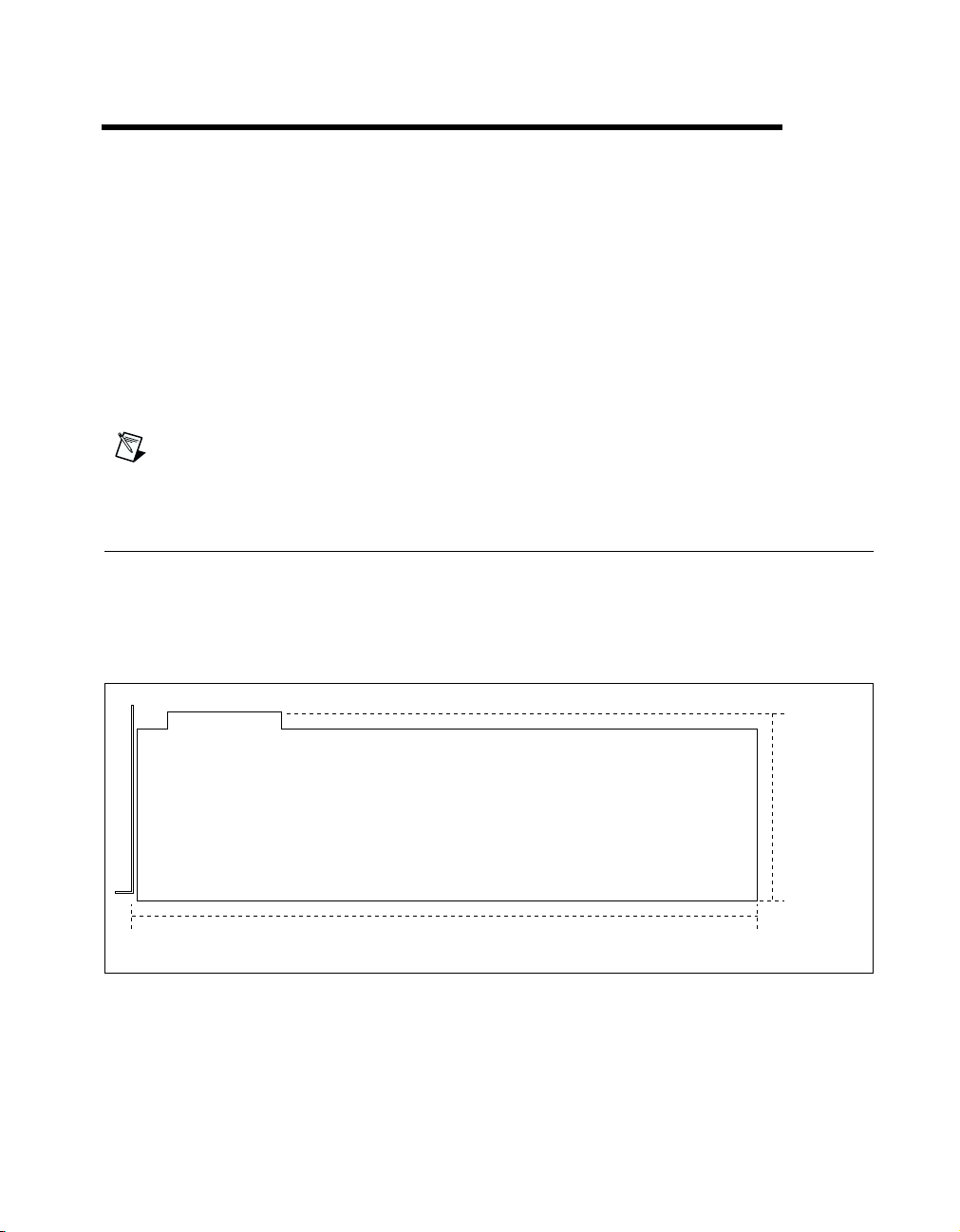
Modifying and Installing
I/O Expansion Boards
This appendix explains how to modify and install an I/O board in the
VXIpc-872 and VXIpc-873 with a nonremovable flash drive. This
information does not apply to the VXIpc-871 or VXIpc-873 with a
removable flash drive.
Note
Throughout this chapter, VXIpc-873 refers only to VXIpc-873 controllers with
nonremovable flash drives.
Height of Plug-In Boards
In general, the VXIpc-872 and VXIpc-873 can accommodate any
standard-size PCI card and any XT-height ISA card. The height of an I/O
card is measured from the bottom of the bus connector to the top of the
board, as shown in Figure D-1.
D
Height
(4.2 in. max)
Length
(13.415 in. maximum)
Figure D-1. I/O Board Dimensions for VXIpc-872 Expansion Slot
Both XT-height ISA cards and PCI cards are 4.2 in. high. The VXIpc-872
and VXIpc-873 do not support AT-height ISA cards, which are 4.8 in. high.
© National Instruments Corporation D-1 VXIpc 870 Series User Manual
Page 80

Appendix D Modifying and Installing I/O Expansion Boards
Installing an I/O Board
This section leads you through the steps to install an expansion board in the
VXIpc-872 and VXIpc-873.
Materials Needed
You need the following items to install the expansion board:
• A user-defined panel is required on the expansion boards based
on National Instruments blank PCI or ISA panels. The panel should be
manufactured from 0.03 in. (0.76 mm) thick 1010 cold rolled steel.
The finish should be 0.0003 in. (0.008 mm) nickel plate over 0.0001
in. (0.003 mm) copper flash. Contact National Instruments if you have
any questions about specifications for user-defined panels.
As an alternative, you can modify the blank panels provided with
the VXIpc-872 and VXIpc-873. Custom panel design services are
available from National Instruments for a nominal fee.
• PEM nut or a 4-40 nut with lock washer (hole diameter should
be 0.125 in. [3.18 mm]).
• 4-40 × 1/4 in. stainless steel panhead screw.
Installation Steps
Follow these steps to install the expansion board:
1. Notice that the VXIpc-872 and VXIpc-873 include one card guide that
can be rotated to secure the top of either a PCI or an ISA plug-in board.
You may use the card guide in either of two locations, depending on
the length of your installed board. Loosen the screw holding the guide
and rotate the guide to the uppermost position for PCI boards or the
lowermost position for ISA boards. See Figure D-2.
2. Replace the manufacturer-supplied panel bracket with the custom
bracket. The two holes in the bracket align with existing holes in the
VXIpc-872 or VXI-pc873 front panel.
3. Seat the board firmly in one of the expansion bus connectors.
4. Attach the board to the front panel with the two screws. You can use a
PEM nut on the back (far) side of the bracket, or a 4-40 nut with a lock
washer (hole diameter should be 0.125 in.). In either case, use a
4-40 × 1/4 in. stainless steel panhead screw to mount the board/bracket
assembly to the front panel.
VXIpc 870 Series User Manual D-2 www.ni.com
Page 81
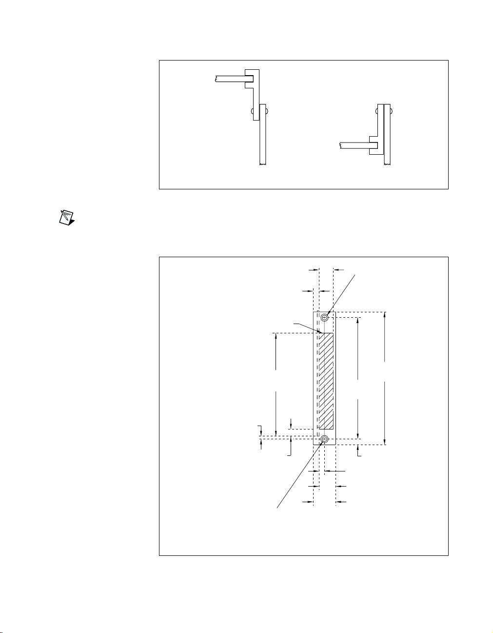
Appendix D Modifying and Installing I/O Expansion Boards
a. PCI Board Installed b. ISA Board Installed
Figure D-2. PCI Board and ISA Board Installed in a VXIpc-872 or VXIpc-873
Note
In the following drawings, dimensions are given in inches and millimeters, with the
millimeter dimensions in square brackets.
(I/O Connector Window)
Window, (.475 [12.07] X
.09 [2.3]
1
Install PEM self-clinching nut, P/N CLS-440-0, per
manufacturer's specifications, far side, or drill
through ø.125 [3.18] for 4-40 screw and nut.
.475 [12.07]
(.200 [5.08])
I/O Connector
3.224 [81.89])
3.464
[87.99]
.240 [6.10]
1
1
4.080
[103.63]
.180 [4.57]
.560 [14.22]
.760 [19.30]
4.46
[113.28]
.19 [4.8]
Figure D-3. Front View of PCI Board Expansion Bracket
© National Instruments Corporation D-3 VXIpc 870 Series User Manual
Page 82
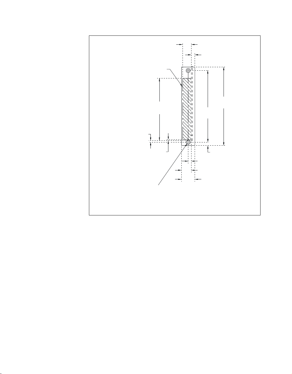
Appendix D Modifying and Installing I/O Expansion Boards
(I/O Connector Window)
.490 [12.45]
I/O Connector
(.200 [5.08])
Window, (490 [12.45] X
3.500 [88.90])
3.550
[90.17]
4.080
[103.63]
.09 [2.3]
.050 [1.27]
.180 [4.57]
.560 [14.22]
.760 [19.30]
1
1
Install PEM self-clinching nut, P/N CLS-440-0, per
manufacturer's specifications, far side, or drill
through ø.125 [3.18] for 4-40 screw and nut.
4.46
[113.28]
.19 [4.8]
Figure D-4. Front View of ISA Board Expansion Bracket
VXIpc 870 Series User Manual D-4 www.ni.com
Page 83

Common Questions
This appendix answers common questions you may have when using the
VXIpc 870 Series.
What do the LEDs on the front of the VXIpc 870 Series mean?
Refer to Appendix B, LED Indicators, for a description of the front
panel LEDs.
Is something wrong if the red SYSF and FAIL LEDs stay lit after
booting the VXIpc 870 Series?
If either the SYSF or FAIL LED remains lit, refer to Appendix B, LED
Indicators, for troubleshooting steps.
Can I access 32-bit registers in my VXIbus system from the VXIpc 870
Series?
Yes. The VXIpc 870 Series uses the 32-bit PCI bus to interface to the
VXIbus. In fact, its VXIbus circuitry also supports the VME64 standard for
D64 accesses.
E
What kind of signal is CLK10 and what kind of signal do I need for an
external CLK10?
CLK10 is a differential ECL signal on the backplane. However, because
the oscillator and the EXTCLK input on the front panel use TTL levels,
you need to supply a TTL-level signal for EXTCLK. Our voltage
converters convert the signal to differential ECL.
What is the accuracy of the CLK10 signal?
The CLK10 signal generated by the VXIpc 870 Series is ±100 ppm (0.01%)
as per the VXIbus specification. If you need a more accurate CLK10 signal,
you can use the CLKI/O connector on the front panel.
© National Instruments Corporation E-1 VXIpc 870 Series User Manual
Page 84

Appendix E Common Questions
What if my keyboard connector does not fit into the keyboard port?
You can plug keyboards that have a 6-pin PS/2 type connector directly into
the VXIpc 870 Series. Your kit also includes a keyboard adapter cable that
you can use to adapt the larger AT keyboard connector to the 6-pin PS/2
connector.
What do I need to do if I want to install the VXIpc 870 Series in a slot
other than Slot 0?
The VXIpc 870 Series automatically detects whether it is in Slot 0 of a
VXIbus mainframe. You do not need to change jumper settings to install
the device in a slot other than Slot 0 unless you have defeated the first slot
detector (FSD) circuitry by changing the J22 jumper setting.
Remember that devices in all other slots must not be manually configured
as System Controller (Slot 0) devices. They must be configured either for
automatic first slot detection or manual non-System Controller.
Refer to Chapter 2, Configuration and Installation, for information on
enabling and defeating the FSD circuitry.
How do I check the configuration of the memory, floppy drive, hard
drive, time/date, and so on?
You can view these parameters in the BIOS setup. To enter the BIOS setup,
reboot the VXIpc 870 Series and press the <DEL> key during the memory
tests. Refer to Chapter 6, BIOS, for more information.
How can I boot from an external SCSI hard drive?
In the BIOS setup change the boot sequence to SCSI.
Can I boot off the CD-ROM of the VXIpc 870?
Yes, by changing the boot sequence to CD-ROM in the BIOS setup. Refer
to Chapter 6, BIOS, for more information.
Can I use the internal IDE drive and an external SCSI hard drive at
thesametime?
Yes, you can select which device to boot from in the BIOS setup. Refer to
Chapter 6, BIOS, for information on entering BIOS.
VXIpc 870 Series User Manual E-2 www.ni.com
Page 85

Appendix E Common Questions
My CMOS is corrupted. How do I set it back to default?
1. Enter the BIOS setup program as described in Chapter 6, BIOS.
2. Select Optimal Defaults.
3. Select Save and Exit.
My operating system is damaged but my hard drive is OK. How can
I re-install the operating system?
Do the following:
1. Make a bootable floppy disk. Make sure the disk contains
deltree
2. Boot the machine from the disk.
3. Run
except
deltree C:\*.*
C:\Images
and answer yes to all files and directories
.
• If using Windows NT:
Go to
C:\Images\os\wint\I386
directory and run
Winnt /B
• If using Windows 98:
Go to
C:\Images\os\Win98
4. Install all IO drivers from
C:\Images\VXI870\...
and run
Setup
.
.
.
What about running Resman?
Resman is the name of the utility that performs the duties of a VXI
Resource Manager as discussed in the VXIbus specification. When you
set a National Instruments controller to Logical Address 0, you will at some
point need to run Resman to configure your VXI instruments. If your
controller uses a different (non-zero) logical address and is a
message-based device, start Resman before running it on the Logical
Address 0 computer.
When do you need to run Resman?
Run Resman whenever you need to configure your VXI instruments. For
example, if you power-cycle your VXI/VME chassis, your instruments will
be reset, and you will need to run Resman to configure them. You can get
into trouble if you run Resman when your devices are not in a reset state.
Therefore, if you have to run Resman after running it once, you should reset
allofyourVXIinstruments.
You can perform resource manager operations from within T&M Explorer.
Additionally, you can tell T&M Explorer to run Resman when the
computer first boots up. In this case you may never need to run Resman
explicitly again. You can configure the computer to run Resman at startup,
© National Instruments Corporation E-3 VXIpc 870 Series User Manual
Page 86

Appendix E Common Questions
so when you power the chassis, Resman runs. If you power-cycle the
chassis, the PC reboots, forcing Resman to run again.
How do I handle VME devices?
Although there is no way to automatically detect VME devices in a system,
you can add them easily through the Add Device Wizard in T&M
Explorer. Through this procedure, you can reserve resources for each of
your VME devices and configure T&M Explorer to show VME devices
on the screen with all your other devices.
How can I determine which version of the NI-VXI/VISA software
I have installed?
Following are several ways to find this information:
• From T&M Explorer, select About... from the Help menu. In the
About dialog box, press the Software Info button. This displays
version information on NI-VXI and NI-VISA files.
• Under Windows NT and Windows 98, you can find version
information by right-clicking on any component and selecting the
Properties option. This displays a property sheet with a version tab.
This tab has version information about the product (NI-VXI) and the
component (
NIVXINT.DLL
, for example).
• You can find version information about the NI-VXI driver by running
the VIC utility program. Type
at the prompt, and the utility
ver
displays the versions of VIC and NI-VXI, and the latest VXIpc
hardware revision that this NI-VXI driver supports.
• You can find version information about the VISA driver through
VISAIC by selecting About... from the Help menu.
How can I determine the serial number and hardware revision of the
VXIpc embedded computers?
Run T&M Explorer and right-click on the name of the VXIpc. Select
Hardware Configuration, and T&M Explorer displays the dialog box for
the device. The title bar includes the serial number and hardware revision.
Which NI-VXI utility program must I use to configure the VXIpc 870
Series?
Use the T&M Explorer program to configure the VXIpc. T&M Explorer is
located in the
VXIpc 870 Series User Manual E-4 www.ni.com
program group folder.
NIVXI
Page 87

Appendix E Common Questions
Which NI-VXI utility program must I use to initialize the VXIpc 870
Series?
In Windows NT/98, the VXIpc embedded computer is automatically
initialized at system startup.
Which NI-VXI utility program must I use to perform startup Resource
Manager operations?
Use the Resman program to perform startup Resource Manager operations.
It is located in the
directory. Resman uses the settings configured
NIVXI
in T&M Explorer. It initializes your VXIbus system and stores the
information that it collects to the
of the
NIVXI
directory.
RESMAN.TBL
file in the
subdirectory
TBL
You can also run Resource Manager operations from T&M Explorer.
Through T&M Explorer, you can also configure Resman to run
automatically at computer startup.
What can I do to make sure that my system is up and running?
The fastest method for testing the system is to run Resman. This program
attempts to access memory in the upper A16 address space of each device
in the system. If Resman does not report any problems, the VXI
communication system is operational.
To test individual devices, you can use the VIC or VISAIC program
to interactively issue NI-VXI functions or NI-VISA operations,
respectively. You can use the
VXIinReg()
and
VXIoutReg()
VXIin()
and
VXIout()
functions or the
functions to test register-based devices by
programming their registers. If you have any message-based devices, you
can send and receive messages with the
WSwrt()
and
WSrd()
functions.
Finally, if you are using LabVIEW or LabWindows/CVI and you have
instrument drivers for the devices in your chassis, you can use the
interactive features of these programs to quickly test the functionality
of the devices.
© National Instruments Corporation E-5 VXIpc 870 Series User Manual
Page 88

Technical Support Resources
This appendix describes the comprehensive resources available to you in
the Technical Support section of the National Instruments Web site and
provides technical support telephone numbers for you to use if you have
trouble connecting to our Web site or if you do not have internet access.
NI Web Support
To provide you with immediate answers and solutions 24 hours a day,
365 days a year, National Instruments maintains extensive online technical
support resources. They are available to you at no cost, are updated daily,
and can be found in the Technical Support section of our Web site at
www.ni.com/support
Online Problem-Solving and Diagnostic Resources
• KnowledgeBase—A searchable database containing thousands of
frequently asked questions (FAQs) and their corresponding answers or
solutions, including special sections devoted to our newest products.
The database is updated daily in response to new customer experiences
and feedback.
• Troubleshooting Wizards—Step-by-step guides lead you through
common problems and answer questions about our entire product line.
Wizards include screen shots that illustrate the steps being described
and provide detailed information ranging from simple getting started
instructions to advanced topics.
• Product Manuals —A comprehensive, searchable library of the latest
editions of National Instruments hardware and software product
manuals.
• Hardware Reference Database—A searchable database containing
brief hardware descriptions, mechanical drawings, and helpful images
of jumper settings and connector pinouts.
• Application Notes—A library with more than 100 short papers
addressing specific topics such as creating and calling DLLs,
developing your own instrument driver software, and porting
applications between platforms and operating systems.
F
© National Instruments Corporation F-1 VXIpc 870 Series User Manual
Page 89

Appendix F Technical Support Resources
Software-Related Resources
• Instrument Driver Network—A library with hundreds of instrument
drivers for control of standalone instruments via GPIB, VXI, or serial
interfaces. You also can submit a request for a particular instrument
driver if it does not already appear in the library.
• Example Programs Database—A database with numerous,
non-shipping example programs for National Instruments
programming environments. You can use them to complement the
example programs that are already included with National Instruments
products.
• Software Library —A library with updates and patches to application
software, links to the latest versions of driver software for National
Instruments hardware products, and utility routines.
Worldwide Support
National Instruments has offices located around the globe. Many branch
offices maintain a Web site to provide information on local services. You
can access these Web sites from
www.ni.com/worldwide
If you have trouble connecting to our Web site, please contact your local
National Instruments office or the source from which you purchased your
National Instruments product(s) to obtain support.
For telephone support in the United States, dial 512 795 8248. For
telephone support outside the United States, contact your local branch
office:
Australia 03 9879 5166, Austria 0662 45 79 90 0, Belgium 02 757 00 20,
Brazil 011 284 5011, Canada (Calgary) 403 274 9391,
Canada (Ontario) 905 785 0085, Canada (Québec) 514 694 8521,
China 0755 3904939, Denmark 45 76 26 00, Finland 09 725 725 11,
France 01 48 14 24 24, Germany 089 741 31 30, Greece 30 1 42 96 427,
Hong Kong 2645 3186, India 91805275406, Israel 03 6120092,
Italy 02 413091, Japan 03 5472 2970, Korea 02 596 7456,
Mexico (D.F.) 5 280 7625, Mexico (Monterrey) 8 357 7695,
Netherlands 0348 433466, New Zealand 09 914 0488,
Norway 32 27 73 00, Poland 0 22 528 94 06, Portugal 351 1 726 9011,
Singapore 2265886, Spain 91 640 0085, Sweden 08 587 895 00,
Switzerland 056 200 51 51, Taiwan 02 2528 7227,
United Kingdom 01635 523545
VXIpc 870 Series User Manual F-2 www.ni.com
Page 90

Glossary
Prefix Meanings Value
p- pico- 10
n- nano- 10
µ- micro- 10
m- milli- 10
k- kilo- 10
M- mega- 10
G- giga- 10
t- tera- 10
Symbols
° degrees
–12
–9
– 6
–3
3
6
9
12
Ω ohms
A
A amperes
A24 space VXIbus address space equivalent to the VME 16 MB standard address
space
A32 space VXIbus address space equivalent to the VME 4 GB extended address space
address character code that identifies a specific location (or series of locations) in
memory
© National Instruments Corporation G-1 VXIpc 870 Series User Manual
Page 91

Glossary
address space a set of 2nmemory locations differentiated from other such sets in
VXI/VMEbus systems by six addressing lines known as address modifiers.
n is the number of address lines required to uniquely specify a byte location
in a given space. Valid numbers for n are 16, 24, and 32. In VME/VXI,
because there are six address modifiers, there are 64 possible address
spaces.
ANSI American National Standards Institute
API Application Programming Interface; the direct interface that an end user
sees when creating an application
ASD Acceleration Spectral Density; a calculation of random vibration intensity
across a frequency bandwidth
ASIC application-specific integrated circuit—a proprietary semiconductor
component designed and manufactured to perform a set of specific
functions for a specific customer
B
bbit—one binary digit, either 0 or 1
Bbyte—eight related bits of data, an 8-bit binary number. Also used to denote
the amount of memory required to store one byte of data.
backplane an assembly, typically a printed circuit board, with 96-pin connectors and
signal paths that bus the connector pins. A C-size VXIbus system will have
two sets of bused connectors called J1 and J2. A D-size VXIbus system will
have three sets of bused connectors called J1, J2, and J3.
BERR* bus error signal
BIOS Basic Input/Output System. BIOS functions are the fundamental level
of any PC or compatible computer. BIOS functions embody the basic
operations needed for successful use of the computer’s hardware resources.
bus the group of conductors that interconnect individual circuitry in a computer.
Typically, a bus is the expansion vehicle to which I/O or other devices are
connected. Examples of buses include the ISA bus, PCI bus, VXI bus, and
VME bus.
VXIpc 870 Series User Manual G-2 www.ni.com
Page 92

Glossary
bus error an error that signals failed access to an address. Bus errors occur with
low-level accesses to memory and usually involve hardware with bus
mapping capabilities. For example, nonexistent memory, a nonexistent
register, or an incorrect device access can cause a bus error.
C
CCelsius
CLK10 a 10 MHz, ±100 ppm, individually buffered (to each module slot),
differential ECL system clock that is sourced from Slot 0 of a VXIbus
mainframe and distributed to Slots 1 through 12 on P2. It is distributed to
each slot as a single-source, single-destination signal with a matched delay
of under 8 ns.
CMOS Complementary Metal Oxide Semiconductor; a process used in making
chips
D
DIN Deutsches Institut für Normung—German Standards Institute
DMA Direct Memory Access; a method by which data is transferred between
devices and internal memory without intervention of the central processing
unit. DMA is the fastest method of transferring data to/from computer
memory.
DRAM Dynamic RAM (Random Access Memory); storage that the computer must
refresh at frequent intervals
E
ECL Emitter-Coupled Logic
EDO Extended Data Out; a DRAM architecture that shortens overall access
latency, improving performance
EEPROM Electronically Erasable Programmable Read Only Memory—ROM that
can be erased with an electrical signal and reprogrammed
© National Instruments Corporation G-3 VXIpc 870 Series User Manual
Page 93

Glossary
embedded controller an intelligent CPU (controller) interface plugged directly into the VXI
backplane, giving it direct access to the VXIbus. It must have all of its
required VXI interface capabilities built in.
EMC electromagnetic compliance
EMI electromagnetic interference
external trigger a voltage pulse from an external source that triggers an event
F
fair requester a VXIbus device that willnot arbitrate for the VXIbus after releasing it until
it detects the bus request signal inactive. This ensures that all requesting
devices will be granted use of the bus.
G
g1.grams
2. A measure of acceleration equal to 9.8 m/s
GPIB General Purpose Interface Bus (IEEE 488)
g
RMS
A measure of random vibration. The root mean square of acceleration
levels in a random vibration test profile.
2
H
hex hexadecimal; the numbering system with base 16, using the digits 0 to 9
and letters A to F
Hz hertz; cycles per second
I
IDE Integrated Drive Electronics. Denotes the most common interface to the
hard drive on PCs.
IEC International Electrotechnical Commission. The IEC publishes
internationally recognized standards. IEC 60068 contains information on
environmental testing procedures and severities.
VXIpc 870 Series User Manual G-4 www.ni.com
Page 94

Glossary
IEEE Institute of Electrical and Electronics Engineers
in. inches
I/O input/output; the techniques, media, and devices used to achieve
communication between machines and users
instrument driver a set of routines designed to control a specific instrument or family of
instruments, and any necessary related files for LabWindows/CVI or
LabVIEW
interrupt a means for a device to request service from another device; a computer
signal indicating that the CPU should suspend its current task to service a
designated activity
interrupt handler a VMEbus functional module that detects interrupt requests generated by
interrupters and responds to those requests by requesting status and identify
information
interrupt level the relative priority at which a device can interrupt
IRQ* interrupt signal
ISA Industry Standard Architecture; denotes a common expansion bus used
in PCs
K
Kkilo—(1) the standard metric prefix for 1,000, or 103, used with units of
measure such as volts, hertz, and meters; (2) the prefix for 1,024, or 2
used with B (byte) in quantifying data or computer memory
10
,
L
LED light-emitting diode
© National Instruments Corporation G-5 VXIpc 870 Series User Manual
Page 95

Glossary
M
m meters
Mmega—(1) the standard metric prefix for 1 million or 10
units of measure such as volts and hertz; (2) the prefix for 1,048,576, or 2
6
,whenusedwith
20
when used with B (byte) to quantify data or computer memory
MANTIS a National Instruments custom ASIC that performs VXIbus arbitration and
manages interrupts and triggers
master a functional part of a VME/VXIbus device that initiates data transfers on
the backplane. A transfer can be either a read or a write.
MBLT eight-byte block transfers in which both the Address bus and the Data bus
areusedtotransferdata
MITE a National Instruments custom ASIC, a sophisticated dual-channel DMA
controller that incorporates the Synchronous MXI and VME64 protocols to
achieve high-performance block transfer rates
MODID module ID lines. Used in VXI to geographically locate boards and to
dynamically configure boards
MTBF Mean Time Between Failure
N
NI-488.2 or
NI-488.2M
the National Instruments industry-standard software for controlling GPIB
instruments
,
NI-VISA the National Instruments implementation of the VISA standard; an
interface-independent software that provides a unified programming
interface for VXI, GPIB, and serial instruments
NI-VXI the National Instruments bus interface software for VME/VXIbus systems
Non-Slot 0 device a device configured for installation in any slot in a VXIbus mainframe other
than Slot 0. Installing such a device into Slot 0 can damage the device, the
VXIbus backplane, or both.
VXIpc 870 Series User Manual G-6 www.ni.com
Page 96

Glossary
P
PCI Peripheral Component Interconnect. The PCI bus is a high-performance
32-bit or 64-bit bus with multiplexed address and data lines.
PCMCIA Personal Computer Memory Card International Association
POSC Power-On Self Configuration. A process by which the MITE chip programs
its own registers from EEPROMs at power up
R
Resource Manager a message-based Commander locatedat Logical Address 0, which provides
configuration management services such as address map configuration,
Commander and Servant mappings, and self-test and diagnostic
management
RMS Root mean squared. See g
rms
.
S
s seconds
SCSI Small Computer System Interface (bus)
SIMM Single In-line Memory Module
slave a functional part of a VME/VXIbus device that detects data transfer cycles
initiated by a VMEbus master and responds to the transfers when the
address specifies one of the device’s registers
Slot 0 device a device configured for installation in Slot 0 of a VXIbus mainframe. This
device is unique in the VXIbus system in that it performs the VXI/VMEbus
System Controller functions, including clock sourcing and arbitration for
data transfers across the backplane. Installing such a device into any other
slot can damage the device, the VXIbus backplane, or both.
SMB Sub Miniature Type B connector that features a snap coupling for fast
connection
© National Instruments Corporation G-7 VXIpc 870 Series User Manual
Page 97

Glossary
SYSFAIL A VMEbus signal that is used by a device to indicate an internal failure.
A failed device asserts this line. In VXI, a device that fails also clears its
PASSed bit in its Status register.
T
trigger either TTL or ECL lines used for intermodule communication
TTL Transistor-Transistor Logic
V
V volts
VGA Video Graphics Array; the minimum video display standard for all PCs
VISA Virtual Instrument Software Architecture. This is the general name given to
VISA and its associated architecture.
VME Versa Module Eurocard or IEEE 1014
VXIbus VMEbus Extensions for Instrumentation
VXIpc 870 Series User Manual G-8 www.ni.com
Page 98

Index
A
ACC LED, B-3
adapter cables, 2-2
AGP Graphics, 5-3
application software, 1-5
assembly number (figure), 3-1
automatic-detection configuration, 3-6, E-5
automatic slot detection (J22) (figure), 3-1
B
BIOS
See also CMOS.
boot drive, E-2
checking configuration, E-2
default setup settings, 6-1, E-2
entering setup, 6-1
FAILSAFE defaults, 6-1
features, 6-1
functional overview, 5-5
OPTIMAL defaults, 6-1
block diagram, 5-2
board access LEDs
ACC LED, B-3
DRV LED, B-3
SCSI LED, B-3
bus speed (W4) (figure), 3-1
C
CD-ROM, booting from, E-2
chip set, SDRAM, 5-2
CLK10
configuration, 3-5
definition of, E-1
external clock, 5-7
onboard logic, 3-7
routing and termination, 3-5, 3-7
signal accuracy, E-1
signal generation, 3-7, E-1
synchronization, 5-7
CMOS
See also BIOS
CMOS (W6) (figure), 3-1
PC configuration options, 3-10, E-3
system CMOS, 3-10, E-3
COM1
connector signals, C-10
location and pinouts, C-9
COM2
connector signals, C-10
location and pinouts, C-9
common questions, E-1
compatibility, A-3
compiler symbols for NI-VXI, 4-5
configuration
CLK10 routing and termination, 3-5, 3-7
controller/non-system controller, 3-5
MITE EEPROM, 3-7
trigger input termination, 3-5
VXIpc 870 Series, 3-5, E-4
connectors, C-1
controller/non-system controller
configuration, 3-5
CPU
bus factor, 3-12
bus factor (W1, W3, W5, W7) (figure), 3-1
bus speed, 3-11
Pentium II, support of, 3-12
© National Instruments Corporation I-1 VXIpc 870 Series User Manual
Page 99

Index
D
debugging, 4-6
NI Spy, 4-6
VIC, 4-6
VISAIC, 4-6
device interaction (software
development), 4-2
diagnostic resources, online, F-1
dimensions, A-2
driver software, 1-4
DRV LED, B-3
E
EEPROM, 3-7, 3-8
configuration, 3-5, 3-8
enable, Ethernet serial, 3-2
enable, Ethernet serial (figure), 3-1
fixing an invalid configuration, 3-8
power-on settings, 3-13
electrostatic discharge, 2-1
EMI, A-1
Ethernet
address (figure), 3-1
and SCSI-3, 5-3
connector location and pinouts, C-8
connector signals, C-9
Ethernet LEDs, B-3
100B-T LED, B-3
LNK LED, B-3
RX/TX LED, B-3
Ethernet serial EEPROM
enable (W1) (figure), 3-1
power-on settings, 3-13
expansion
PCI, ISA, 5-4
external clock, 5-7, C-17
external SMBs, C-17
F
FAIL LED, B-1
flash memory
installing and removing a flash storage
card (figure), 2-4
installing and removing in the
VXIpc-873, 2-3
flash protect (W17), 3-1
flash protection, 3-12, 3-13
front panel, C-1, C-2
connectors, C-1
thickness, C-2
functional overview, 5-1
functional shock, A-1
fuse location (figure), 3-1
fuse, main power, changing, 3-14
fused power protection, 5-5
G
GPIB
location and pinouts, connector
signals, C-15
GPIB mating connector, C-15
H
hardware defaults, 3-1
(figure), 3-1
(table), 3-2
hardware switches, accessing, 3-5
I
IDE, E-2
IEEE 488.2/HS488 interface, 5-4
IEEE-1284, C-10
IEEE-488.2, C-15
installation, 2-1
VXIpc 870 Series User Manual I-2 www.ni.com
Page 100

Index
installing
in slot other than Slot 0, E-2
instrument drivers, 1-5
interface status LEDs, B-1
ISA bus card, 5-4
J
jumper settings (table), 3-2
K
keyboard, C-6
adapter cable for, 2-2, E-2
connectors location and pinout, C-6
L
LabVIEW, 1-5
LabWindows/CVI, 1-5, 4-6
LEDs, B-1
100B-T LED, B-3
ACC LED, B-3
and system startup, B-2
board access, B-3
DRV LED, B-3
Ethernet, B-3
FAIL LED, B-1
indicators, B-1
LNK LED, B-3
ONLINE LED, B-1
PWROK LED, B-1
RX/TX LED, B-3
SCSI LED, B-3
SYSF LED, B-1
LNK LED, B-3
locator diagram, 3-1
M
main power fuse, changing, 3-14
memory
installing additional, 3-13
SO-DIMM sockets (figure), 3-1
SO-DIMMs from National Instruments
(note), 3-14
MITE Configuration Enable (S2) (figure), 3-1
MITE EEPROM
See also EEPROM
configuration, 3-7
MITE user configuration (S1) (figure), 3-1
mouse, 2-2, C-6
connectors location and pinout, C-6
MTBF, A-3
N
National Instruments Web support, F-1
NI Spy, 4-6
NI WatchDOG, 3-13, 5-4
NI-VISA
definition, 4-4
NI-VISA User Manual, location of (note), 4-4
NI-VXI
compiler symbols, 4-5
using, E-4
NI-VXI User Manual, location of (note), 4-4
NI-VXI/VISA
determining version, E-4
driver, 4-1
examples (table), 4-4
O
onboard jumper and switch settings
(table), 3-2
onboard logic, 3-7
ONLINE LED, B-1
online problem-solving and diagnostic
resources, F-1
© National Instruments Corporation I-3 VXIpc 870 Series User Manual
 Loading...