

Page 1

Nevion
Lysaker Torg 5
1366 Lysaker
Norway
Tel: +47 33 48 99 99
nevion.com
QUAD-DA-1x2-PB
Quad 1x2 3G/HD/SD-SDI Distribution Amplifier
with Passive Input Bypass
User manual
Rev. D
Page 2

QUAD-DA-1x2-PB Rev. D
nevion.com | 2
Nevion Support
Nevion AS
Lysaker Torg 5
1366 Lysaker, Norway
Support phone 1: +47 33 48 99 97
Support phone 2: +47 90 60 99 99
Nevion USA
400 West Ventura Boulevard, Suite 155,
Camarillo, CA 93010, USA
Toll free North America: (866) 515-0811
Outside North America: +1 (805) 247-8560
E-mail: support@nevion.com
See http://www.nevion.com/support/ for service hours for customer support globally.
Revision history
Current revision of this document is the uppermost in the table below.
Rev.
Repl.
Date
Sign
Change description
D C 2017-12-19
MR
Added new chapter;
4.4 Passive input bypass (-PB)
In chapter 4.2 Terminal format support:
Removed listing of SMPTE 310.
C B 2017-11-17
MR
2.2 Electrical SDI inputs; changed min. cable
lengths for all formats to be in accordance with
current datasheet.
B A 2017-09-27
MR
Corrected value of saturation voltage in
2.4 Open drain GPIOs
Updated index. Lack of update caused error
messages.
Corrected descriptions of GPIO functions in
the following chapters; 4.2, 4.3, 5.1.2
A - 2017-07-14
GAJ/MR
Initial version
Page 3

QUAD-DA-1x2-PB Rev. D
nevion.com | 3
Contents
Revision history ........................................................................................................ 2
1 Product overview ................................................................................................... 4
1.1 Product versions ........................................................................................................... 4
2 Specifications ........................................................................................................ 5
2.1 General ......................................................................................................................... 5
2.2 Electrical SDI inputs ...................................................................................................... 5
2.3 Electrical SDI outputs .................................................................................................... 6
2.4 Open drain GPIOs ......................................................................................................... 6
2.5 Features ........................................................................................................................ 7
2.6 Supported standards ..................................................................................................... 7
3 Configuration ......................................................................................................... 8
3.1 Multicon GYDA configuration ........................................................................................ 8
3.1.1 Card label ................................................................................................................... 9
3.1.2 Firmware upgrade ...................................................................................................... 9
3.1.3 Electrical inputs .......................................................................................................... 9
3.1.4 Reclockers ................................................................................................................. 9
3.1.5 Electrical outputs ................................................................ ........................................ 9
3.2 Configuration through DIP settings ...............................................................................10
3.2.1 Selection of power supply..........................................................................................11
4 Connections ........................................................................................................ 12
4.1 Mounting the connector module ...................................................................................12
4.2 Terminal format support ...............................................................................................13
4.3 GPIO connections ........................................................................................................14
4.4 Passive input bypass (-PB) ..........................................................................................14
5 Operation ............................................................................................................. 15
5.1 Module status ...............................................................................................................15
5.1.1 Multicon GYDA status interface .................................................................................15
5.1.2 GPI ALARM – Module Status Outputs .......................................................................16
5.1.3 Front panel - Status monitoring ................................................................ .................16
General environmental requirements for Nevion equipment .................................. 18
Product Warranty.................................................................................................... 19
Appendix A Materials declaration and recycling information .................................. 20
A.1 Materials declaration ....................................................................................................20
A.2 Recycling information ...................................................................................................20
Page 4
QUAD-DA-1x2-PB Rev. D
nevion.com | 4
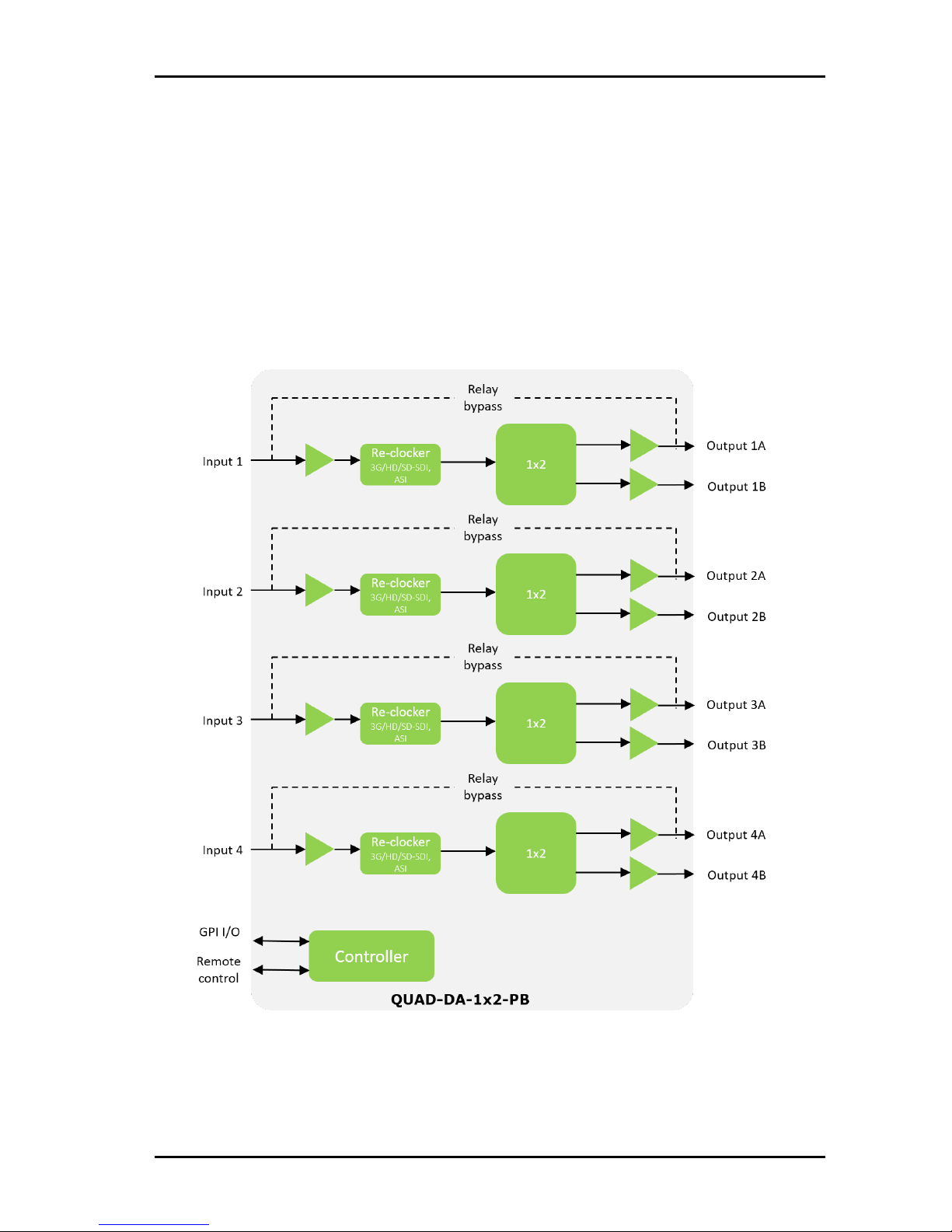
1 Product overview
The QUAD-DA-1x2-PB is a quad 1x2 3G/HD/SD-SDI Distribution amplifier with passive
input bypass well suited for quad stream UHD/4K applications.
The card can operate as either four independent DAs or a quad stream DA monitoring the 4
inputs as one. When operated in quad stream mode the card´s signal alarming will be given
on the combined stream.
A passive relayed bypass of all four main inputs enables signal pass-thru in case of mains
or card failure.
The Flashlink element manager Multicon enables web and SNMP interface for configuring
card settings and monitoring signal status.
Figure 1: Block diagrams of the QUAD-DA-1x2-PB
1.1 Product versions
There are two connector backplane versions, one with DIN 1.0/2.3 and one with HD-BNC
connectors.
Page 5

QUAD-DA-1x2-PB Rev. D
nevion.com | 5
2 Specifications
2.1 General
Power (DC) +5 V / +15 V (Configurable DIP switch setting)
3.0 W / +5 V, 0.6 W / +15 V maximum
2.8 W / +5 V, 0.6 W / +15 V typical
User interface Status LED, Status GPIOs, configuration DIP switches
Web interface and SNMP thru Multicon controller
Operating environmental
temperature 0 to +45 °C
2.2 Electrical SDI inputs
Number of inputs 4, relay protected
Data rate 125 Mbps – 2970 Mbps
Connectors 75 Ohm, DIN 1.0/2.3 or HD-BNC
(depends on backplane type)
Input Return loss < -15 dB, 5 MHz – 1.5 GHz
< -10 dB, 1.5 GHz – 3 GHz
Jitter tolerance SD limit:
10 Hz – 10 kHz: > 1 UI
10 kHz – 10 MHz: > 0.2 UI
HD limit:
10 Hz – 10 kHz: > 1 UI
10 kHz – 10 MHz: > 0.2 UI
3G limit:
10 Hz – 10 kHz: > 2 UI
10 kHz – 10 MHz: > 0.3 UI
Equalized cable lengths SD:
(BER < 10E-12) 280m min. 300m typ. (Belden 8281)
Checkfield pattern 400m min. 450m typ. (Belden 1694A)
HD:
Unused outputs terminated 90m min. 100m typ. (Belden 1694A)
with 75 ohm terminators 3G:
50m min. 55m typ. (Belden 1694A)
Remark The I-xA input signals pass through relays resulting in
degraded levels and rise/fall time equivalent to 15
meters of 1694A cable. The cable lengths above include
this.
Page 6

QUAD-DA-1x2-PB Rev. D
nevion.com | 6
2.3 Electrical SDI outputs
Number of outputs 8, 4 relay protected
Connectors 75 Ohm, DIN 1.0/2.3 or HD-BNC
(depends on backplane type)
Output Return loss < -15 dB, 5 MHz – 1.5 GHz
< -10 dB, 1.5 GHz – 3 GHz
Output signal level 800 mV +/- 10%
Output signal rise / fall time - SD limit: [0.4 ns – 1.5 ns]; < 0.5 ns rise/fall variation
(20% - 80 %) - HD limit: < 270 ps, < 100 ps rise/fall variation
- 3G limit: < 135 ps, < 50 ps rise/fall variation
Remark Due to Nevion’s design philosophy with use of passive
backplanes, the output signals pass significant PCB
trace lengths between the cable drivers and output
ports. This will result in significant degradation of levels
and rise/fall times at HD and 3GHD at the backplane
connectors compared to the listed specifications above
which states launch levels at the cable drivers. The
degradation equals approximately 10 meters of 1694A
cable.
Remark The O-xA outputs pass through relays resulting in
degraded levels and rise/fall time equivalent to 15
meters of 1694A cable.
Amplitude overshoot/undershoot < 10%
Polarity All non-inverting (DVB-ASI compliant)
Output timing jitter SD: < 0.2 UI
HD: < 1 UI
3G: < 1 UI
Output alignment jitter SD: < 0.15 UI
HD: < 0.15 UI
3G: < 0.2 UI
2.4 Open drain GPIOs
Connector PTSA 0,5 mm2 Push-in spring wire connector
No of ports 3
Applied voltage (DC) 25V max.
Permitted current drain
in output “low” state 150 mA max.
Saturation voltage at
max. permitted current drain 600 mV max.
Page 7

QUAD-DA-1x2-PB Rev. D
nevion.com | 7
2.5 Features
Re-clocking: Automatic SD, HD, 3GHD detection
Automatic output slew rate adjustment according to
SMPTE- 259M, SMPTE-292 and SMPTE424M
Supported clock rates: 125Mbps, 270Mbps, 1.485 and 1.485/1.001Gbps, 2.97
and 2.97/1.001Gbps
MADI: According to AES10 with the following exemption;
Amplitude and rise and fall times according to SD-SDI
(SMPTE- 292M) at electrical outputs.
2.6 Supported standards
SMPTE: SMPTE259M, SMPTE292 and SMPTE424M
DVB-ASI: EN50083-9
MADI: AES10
Page 8

QUAD-DA-1x2-PB Rev. D
nevion.com | 8
3 Configuration
Configuration of this card can either be done from Multicon GYDA element manager or locally
on the card by DIP switches.
3.1 Multicon GYDA configuration
Below is a snapshot from the Multicon GYDA interface.
Figure 2: Configuration tab example
Page 9

QUAD-DA-1x2-PB Rev. D
nevion.com | 9
3.1.1 Card label
Figure 3: Card label
Assign a name to the Flashlink module, up to 31 characters. When the “locate card” button
is pushed, all indicators/LED’s on the front of the module will flash for 120 seconds,
alternatively a period can be entered into the sec box.
3.1.2 Firmware upgrade
Figure 4: Firmware upgrade
Update the firmware on the Flashlink module. The firmware file first has to be uploaded to
Multicon Gyda by ftp. See user manual for Multicon Gyda concerning help on uploading.
3.1.3 Electrical inputs
Figure 5: Electrical inputs
For SDI signals set the electrical input to “normal”. For non-supported signal formats
“bypass” mode may be used. The cable equalizer will then be bypassed. This may give
better performance since the cable equalizer is optimized for the supported standards.
3.1.4 Reclockers
Figure 6: Reclockers
For supported formats; set to enable, else it may be set to bypass. Autobypass only works if
the reclocker is enabled. In “autobypass” mode the reclocker will bypass not supported
formats.
3.1.5 Electrical outputs
Figure 7: Electrical outputs
With slew rate set to “Auto” the rise- and fall time of the cable driver will be automatically
adjusted according to the actual signal format.
For bit rates below 270Mbps the slew rate is automatically set to SD slew rate.For not
supported signals with bitrates above 270Mbps the proper slew rate can be selected
manually.
Page 10

QUAD-DA-1x2-PB Rev. D
nevion.com | 10
3.2 Configuration through DIP settings
The correct configuration can either be set with the DIP switch on the card or through the
GYDA Control System. The layout is shown in the drawing below with the DIP switch to the
upper left position.
Figure 8: QUAD-DA-1x2-PB board layout
Figure 9: DIP switch
Page 11

QUAD-DA-1x2-PB Rev. D
nevion.com | 11
Table 1: DIP settings
Switch #
Label
Function, DIP=OFF
Function, DIP=ON
Comment
1
+15V
Board supplied by
+15 V DC
Board supplied by
+5 V DC
Selection of power
Attention:
Must only be operated
when the board is
unpowered
2 1 Not used
Not used
3 2 Not used
Not used
4 3 Not used
Not used
5
4
Reclocker Bypass
(Loss of lock will not
work on this mode)
Reclocker ON
Reclocker mode
6
5
Cable Equalizer
Bypass
(Loss of signal will not
work on this mode)
Cable Equalizer
ON
Equalizer mode
7 6 Not used
Not used
8
OVR
GYDA control.
Config. with GYDA
Override GYDA
control Config. with
DIP switch
Select config. from
GYDA
All DIP switches are off when pointing towards the release handle.
3.2.1 Selection of power supply
(Only DIP configurable)
The module can be configured to be powered from either +5 V or +15 V DC power rails with
DIP switch labeled “+15V”. This feature is useful to improve utilization of, or balancing the
available power in a frame.
The DIP switch must only be operated when the board is unpowered
to prevent instability.
The configuration is set to +5 V as default.
Page 12

QUAD-DA-1x2-PB Rev. D
nevion.com | 12
4 Connections
The QUAD-DA-1x2-PB has a dedicated connector module; DA-CHO-C1 and –C2/-C3. This
module is mounted at the rear of the sub-rack. The layout of the module is shown in the figure
below.
Figure 10: Backplane connector module for QUAD-DA-1x2-PB
• Passive input bypass is connected through the I-xA to O-xA connectors
respectively, where x is the stream number from 1 to 4.
• In QUAD-DA-1x2-PB, the I/O-xB connectors are O-xB outputs, while in
QUAD-CHO-2x1-PB the I/O-xB connectors are I-xB inputs.
4.1 Mounting the connector module
Product consists of three main parts as seen in Figure 11.
Figure 11: the three main parts of the product
Page 13

QUAD-DA-1x2-PB Rev. D
nevion.com | 13
Some assembly is needed before this can be installed into a frame:
1. Connect connector module (3, Figure 11) to relay module (2, Figure 11) and make
sure the connectors are completely mated with the two guide pins located on
top/bottom as seen in Figure 11.
2. Slide the assembled modules into the back of the frame while making sure the C1
board slides correctly into the frame’s guide rail. Make sure the pins align and
correctly connects to the power bus connector as seen in Figure 12.
3. Fasten the backplane with the supplied screws.
More details on how the connector module is mounted, are found in the user manual for the
sub-rack frame FR-2RU-10-2.
This manual is also available from our web site: http://www.nevion.com
Figure 12: Instalment from the back of the frame
(NB: Picture of CONV-SFP-4, but the procedure is equal).
4.2 Terminal format support
The different input and output ports on QUAD-DA-1x2-PB can support a number of formats.
The table below show which signal formats are supported on the selected terminals.
Unused input and output ports should be terminated with 75 Ohm terminators.
Table 2: Signal support
Terminal
Function
Supported Format
Mode
I-xA
(x = 1,2,3,4)
Electrical Input
SDI, DVB-ASI, Transparent
Input
O-xA
I/O-xB
(x = 1,2,3,4)
Electrical Output
Reclocked Output
SDI, DVB-ASI, Transparent
Output
GPIO-(2-3)
Status
Wired alarms
Open Drain
output
GPIO-5
Module status
Wired alarms
Open drain
0utput
Page 14

QUAD-DA-1x2-PB Rev. D
nevion.com | 14
4.3 GPIO connections
GPI connector is shown in figures below.
Table 3: QUAD-DA-1x2-PB module GPI pinning
Signal
Function
Pin #
Mode
GPIO-1 /
Status
Not used
Pin 1
GPIO-2
Reflects “Info 1” LED. See also
5.1.2
Pin 2
Open drain
GPIO-3
Reflects “Info 2” LED. See also
5.1.2
Pin 3
Open drain
GPIO-4
Not used
Pin 4
Open drain
GPIO-5
Module status, reflects the status
LED. See also 5.1.2
Pin 5
Open drain
Ground
0V / gnd pin
Pin 8
0V
Figure 13: GPI connector
4.4 Passive input bypass (-PB)
The equalized cable lengths specified under chapter “2.2 Electrical SDI inputs” are valid only
when the main board is active and are based on the equalizing properties of the specific
cable equalizer solution used in this product.
When utilizing the “Passive input bypass” solution, the sum of cable lengths from the source
via the relay inside QUAD-CHO-2x1-PB to the next product in the chain must be dimensioned
according to the equalizing properties of this next product.
It is strongly recommended to perform thorough testing of the function before taking it into
use.
Page 15

QUAD-DA-1x2-PB Rev. D
nevion.com | 15
5 Operation
5.1 Module status
The status of the module can be monitored in three ways.
1. Multicon GYDA System Controller (optional).
2. GPI at the rear of the sub-rack.
3. LEDs at the front of the sub-rack.
Of these three, the GPI and the LEDs are mounted on the product itself, whereas the Multicon
GYDA System Controller is a separate module giving detailed information on the card status.
5.1.1 Multicon GYDA status interface
Figure 14: Status tab example
Page 16

QUAD-DA-1x2-PB Rev. D
nevion.com | 16
The on-board temperature measurement is a feature used for monitoring
variations in temperature over time and can be accessed thru SNMP. The
absolute value of the temperature measurement has little value of its own as it
does not reflect the temperature inside the electronics nor the ambient frame
temperature.
When +5V is chosen as supply source, the presented current value for +15V will
be approximately 0.04A due to current drain of the four high frequency relays.
If a reclocker is configured to “Bypass” mode and a recognizable signal rate is
applied, the shown info will be “Locked” and “Actual rate” though the signal is not
reclocked. Otherwise the shown info will be “Bypass” and no rate information.
5.1.2 GPI ALARM – Module Status Outputs
These outputs can be used for wiring up alarms for third party control systems. All GPIO
outputs are of open drain type.
Open drain GPIO (#5) function:
This output is low ohmic referred to GND when no severe system errors are detected
and high ohmic in opposite situation and when no main board is connected
Open drain GPIOs (#2-3) function:
These outputs reflect the status on LEDs “INFO 1-2” respectively as follows;
- Low ohmic referred to GND when LED is green or orange
- High ohmic referred to GND when LED is red
Open drain GPIO #5 function:
This output reflects the status on the “Status” LED as follows;
- Low ohmic referred to GND when LED is green
- High ohmic referred to GND when LED is red
5.1.3 Front panel - Status monitoring
The status of the module can be easily monitored visually by the LEDs at the front of the
module. The LEDs are visible through the front panel of FR-2RU-10-2(-MkII) as shown in
the figure below.
Figure 15: Front panel LEDs
Page 17

QUAD-DA-1x2-PB Rev. D
nevion.com | 17
Table 4: Front panel LEDs
LED \
State
Red
Orange
Green
No light
Comment
Status
Module is faulty,
or module is
initializing
N/A
Module is OK
Module power
is OK
Module
has no
power
INFO 1
Loss Of Signal,
all inputs
1-3 Inputs
Loss Of Signal
Signal present
at all inputs
N/A
All Input
Equalizer
alarms OR’ed
INFO 2
Loss Of Lock,
all inputs
1-3 Inputs
Loss Of Lock
Lock present
at all inputs
N/A
All Input
Reclocker
alarms OR’ed
INFO 3
Not used
Not used
Not used
Constant
Page 18

QUAD-DA-1x2-PB Rev. D
nevion.com | 18
General environmental requirements for Nevion equipment
1.
The equipment will meet the guaranteed performance specification under the
following environmental conditions:
-
Operating room temperature range:
0°C to 45°C
-
Operating relative humidity range:
<90% (non-condensing)
2.
The equipment will operate without damage under the following environmental
conditions:
-
Temperature range:
-10°C to 55°C
-
Relative humidity range:
<95% (non-condensing)
Page 19

QUAD-DA-1x2-PB Rev. D
nevion.com | 19
Product Warranty
The warranty terms and conditions for the product(s) covered by this manual follow the
General Sales Conditions by Nevion, which are available on the company web site:
www.nevion.com
Page 20

QUAD-DA-1x2-PB Rev. D
nevion.com | 20
Appendix A Materials declaration and recycling
information
A.1 Materials declaration
For product sold into China after 1st March 2007, we comply with the “Administrative Measure
on the Control of Pollution by Electronic Information Products”. In the first stage of this
legislation, content of six hazardous materials has to be declared. The table below shows
the required information.
組成名稱
Part Name
Toxic or hazardous substances and elements
鉛
Lead
(Pb)
汞
Mercury
(Hg)
镉
Cadmium
(Cd)
六价铬
Hexavalent
Chromium
(Cr(VI))
多溴联苯
Polybrominated
biphenyls
(PBB)
多溴二苯醚
Polybrominated
diphenyl ethers
(PBDE)
QUAD-DA-1x2-PB
O O O O O
O
O: Indicates that this toxic or hazardous substance contained in all of the homogeneous materials for this part is
below the limit requirement in SJ/T11363-2006.
X: Indicates that this toxic or hazardous substance contained in at least one of the homogeneous materials used
for this part is above the limit requirement in SJ/T11363-2006.
This is indicated by the product marking:
A.2 Recycling information
Nevion provides assistance to customers and recyclers through our web site
http://www.nevion.com/. Please contact Nevion’s Customer Support for assistance with
recycling if this site does not show the information you require.
Where it is not possible to return the product to Nevion or its agents for recycling, the following
general information may be of assistance:
Before attempting disassembly, ensure the product is completely disconnected from
power and signal connections.
All major parts are marked or labeled to show their material content.
Depending on the date of manufacture, this product may contain lead in solder.
Some circuit boards may contain battery-backed memory devices.
 Loading...