

Page 1
DWC-HD
HD-SDI to SD-SDI Down-converter
(with optional Audio De-embedding)
User manual
Rev. 5
Page 2

DWC-HD Rev. 5
nevion.com | 2
Nevion Support
Nevion Europe
P.O. Box 1020
3204 Sandefjord, Norway
Support phone 1: +47 33 48 99 97
Support phone 2: +47 90 60 99 99
Nevion USA
1600 Emerson Avenue
Oxnard, CA 93033, USA
Toll free North America: (866) 515-0811
Outside North America: +1 (805) 247-8560
E-mail: support@nevion.com
See http://www.nevion.com/support/ for service hours for customer support globally.
Revision history
Current revision of this document is the uppermost in the table below.
Rev.
Repl.
Date
Sign
Change description
5 4 2011-01-03
AA
New template.
4 3 2008-12-15
NBS
Added more information about minimum delay.
3 2 2008-11-24
NBS
Corrected number of SDI outputs in Chapter 1;
Corrected table in Chapter 5;
Added specification of minimum delay in Chapter 2.
2 1 2008-07-09
NBS
Added Block diagram in Chapter 1.
1 0 2008-06-18
NBS
Removed monitoring versions.
0 - 2008-06-12
TB
First version for public release.
Page 3

DWC-HD Rev. 5
nevion.com | 3
Contents
1 Product overview ..................................................................................................... 4
1.1 Product versions .............................................................................................................. 4
2 Specifications .......................................................................................................... 6
3 Description ............................................................................................................... 9
3.1 Data path ......................................................................................................................... 9
3.2 Video blocks overview ................................................................................................... 10
3.3 Optical/ Electrical input selection ................................................................................... 10
3.4 De-glitcher ..................................................................................................................... 10
3.5 Scaling block ................................................................................................................. 11
3.6 Frame synchronizer ....................................................................................................... 11
3.7 Video generator ............................................................................................................. 13
3.8 Video processing block .................................................................................................. 14
3.9 EDH processing block ................................................................................................... 14
3.10 Video output selection ................................................................................................. 14
3.11 Video DAC ................................................................................................................... 14
3.12 Audio overview ............................................................................................................ 15
3.13 Audio de-embedder ..................................................................................................... 16
3.14 Audio delay .................................................................................................................. 16
3.15 Audio cross point matrix .............................................................................................. 16
3.16 Audio fallback options .................................................................................................. 16
3.17 Audio generator ........................................................................................................... 16
3.18 Audio processing block ................................................................................................ 16
3.19 Audio embedder .......................................................................................................... 17
3.20 Analog audio output ..................................................................................................... 17
4 Configuration ......................................................................................................... 18
4.1 DIP switch functions ...................................................................................................... 18
4.2 FACTORY reset function ............................................................................................... 19
4.3 GYDA mode .................................................................................................................. 20
5 Connections ........................................................................................................... 22
6 Operation ............................................................................................................... 23
6.1 Front panel LED indicators ............................................................................................ 23
6.2 RS422 commands ......................................................................................................... 23
General environmental requirements for Nevion equipment..................................... 31
Product Warranty ...................................................................................................... 32
Appendix A Materials declaration and recycling information..................................... 33
EC Declaration of Conformity ................................................................................... 34
Page 4
DWC-HD Rev. 5
nevion.com | 4
1 Product overview
The Flashlink DWC-HD-DMUX converts an HD-SDI input signal to an SD-SDI output signal
with user selectable aspect ratio.
Two digital outputs and a set of configurable analog video outputs are provided, all of which
can be set to output the SD signal or the re-clocked original HD signal.
For SD input the card will act as an SD frame synchronizer with an adjustable delay relative
to the sync signal. This frame synchronizer functionality is also present when downconverting. The card is prepared to accept black & burst or a tri-level signal from the frame.
The DWC-HD-DMUX also has a de-glitcher to give error-free synchronous switching.
The audio embedded in the HD-SDI or SD-SDI stream is de-embedded and can be delayed
relative to video. Each audio channel can be swapped in an audio matrix before they are reembedded in the SD-SDI data output stream. For SD-SDI inputs it is possible to turn
embedding completely off and leave the SDI stream unaltered.
A selection of user parameters of the card can be controlled by switches on the board.
Complete control of all parameters is available by use of the Flashlink RS422 Control
Protocol Version 4, which is supported by the Gyda system controller from software release
2.13.
Figure 1: DWC-HD-DMUX-R block diagram
1.1 Product versions
DWC-HD
HD down-converter. With 2XSDI out, SD/HD analog out, internal
audio handling, and frame synchronizer functionality.
DWC-HD-R
HD down-converter. With high sensitivity 9/125µm single mode
optical input, 2XSDI out, SD/HD analog out, internal audio handling,
and frame synchronizer functionality.
DWC-HD-DMUX
HD down-converter. With 2XSDI out, SD/HD analog out, internal
audio handling, analog stereo out, AES (or RS-422 data) out, and
frame synchronizer functionality.
Page 5

DWC-HD Rev. 5
nevion.com | 5
DWC-HD-DMUX-R HD down-
converter. With high sensitivity 9/125µm single mode
optical input, 2XSDI out, SD/HD analog out, internal audio handling,
analog stereo out, AES (or RS-
422 data) out, and frame
synchronizer functionality.
Page 6

DWC-HD Rev. 5
nevion.com | 6
2 Specifications
Optical SDI input
Data rate optical:
270 – 1485 Mbps
Sensitivity
- HD-SDI (1485 Mbps):
Better than -22dBm
- SD-SDI (270 Mbps):
Better than -22dBm
Detector overload threshold:
Min. -3dBm
Detector damage threshold:
>+1dBm
Optical wavelength:
1200-1620nm
Transmission circuit fiber:
9/125um Single Mode
Connector return loss:
>40dB w/ SM fiber
Connector:
SC/UPC
Electrical SDI input
Connectors
75 Ohm BNC
Equalization
Automatic:
- >300m @270Mbps w/Belden 8281, BER < 10E-12
- >100m @1485Mbps w/Belden 1694A, BER < 10E-12
Input Return loss
>15dB, 5MHz -1.5GHz
Jitter tolerance
- SD limit:
- 10Hz-1kHz: >1 UI
- 10kHz – 5MHz: >0.2 UI
- HD limit:
- 10Hz-100kHz: >1 UI
-
100kHz–10MHz: >0.2 UI
Electrical Sync input
Connector
75 Ohm BNC
Format
Black & Burst, Tri-level
Input Return loss
<-35dB @ < 10MHz,
30dB @ < 30MHz
Electrical SDI outputs
Number of outputs
2
Connectors
75 Ohm BNC
Output Return loss
>15dB, 5MHz -1.5GHz
Output signal level
800mV +/- 10%
Output signal rise /
fall time, 20% - 80%
- SD limit: [0.4ns – 1.5ns]; <0.5ns rise/fall var.
- HD limit: < 270ps, <100ps rise/fall var.
Amplitude overshoot
<10%
Output timing jitter
- SD: <0.2 UI
-
HD: <1 UI
Output alignment jitter
- SD: <0.15 UI
- HD: <0.15 UI
Analog Video output, NTSC/PAL
Number of outputs
1 Component RGB/ YUV or 3 CVBS
Connector
3 x 75R BNC
DC offset
< 0±15mV
Page 7

DWC-HD Rev. 5
nevion.com | 7
White level, NTSC
100±1 IRE
Sync level, NTSC
40±1 IRE
Return loss
> 35dB @ 10MHz, >40dB @ 5MHz
White level, PAL
100±1 IRE
Sync level, PAL
40±1 IRE
Diff gain
<0.5%
Diff phase
<1deg
AM noise
< -60dB
PM noise
< -60dB
S/N
< -60dB
2T K-factor
(2T pulse distortion)
< 0.5%
Luma non-linearity
< 2%
Output resolution
10 bits
Analog Video output, HD
Number of outputs
1 component RGB/ YPbPr
Connector
3 x 75R BNC
DC offset
< 0±15mV
White level
100±1 IRE
Return loss
> 30dB @ 30MHz
Output resolution
10 bits
Analog Audio output
Number of outputs
1 stereo pair
Connectors
2 x WECO audio connectors
Impedance
< 66R
Dynamic range
>100dB(A)
Crosstalk
< -60dB 20Hz-20kHz
THD+N
-70dB
Frequency response
20Hz-20kHz +/- 0.5dB
Output level
24dBu +/- 1dB
Common mode DC
immunity
0 – 48V
Level adjustment range
0 – 24dBu with 1db step
Two tone intermodulation
< -80dB
Output resolution
24 bits
AES output
Number of outputs
1
Connectors
WECO audio connector
Return loss
110R +/-20% 0.1MHz – 6.144MHz
Output jitter
<0.0025UI peak
Supported standards
SD, 270 Mbps
SMPTE 259M, SMPTE 272M-AC
HD, 1485 Mbps
SMPTE 292M, SMPTE 274M, SMPTE 291M, SMPTE 296M,
SMPTE 299M
Analog video
SMPTE 170M, SMPTE 274M, ITU-R. BT.470,
ITU-R. BT.709 Part 2
Centre of picture definition
SMPTE RP187, ITU-R. BT.470
Page 8
DWC-HD Rev. 5
nevion.com | 8
Aspect ratio preservation
SMPTE RP199-1999, SMPTE RP221
Color space conversion
HD: ITU-R. BT.709
SD: ITU-R. BT.601
See also ITU-R. BT.1361 for more information
Video switch point
definition and sync
SMPTE RP168 (tri-level), SMPTE 170M, ITU-R. BT.470
AES
AES3-1996
Optical
SMPTE 297M, SMPTE 292M
EDH
Compliant to SMPTE RP165
Video Payload
Identification
SMPTE 352M-2002
Minimum video signal delay through processing
Input standards
Minimum delay [Field+Lines]
Full frame
Cropped edge
Letterbox (NTSC)
Letterbox (PAL)
Regular input standards:
1920/1080i50
0+10
0+41
0+44
1920/1080i59.94
0+10
0+41
0+44
1280/720p50
0+10
0+41
0+44
1280/720p59.94
0+10
0+41
0+44
Progressive input with low frame rate:
1920/1080p25
1+10
1+41
1+44
1920/108p29.97
1+10
1+41
1+44
1280/720p25
1+10
1+41
1+44
1280/720p29.97
1+10
1+41
1+44
Input standards for telecine converters:
Minimum delay [Frame+Lines]
1920/1080p23.97
1+10
1+41
1+44
1280/720p23.97
1+10
1+41
1+44
Other
Power consumption
5V – 5.3W (4.9W without optical receiver)
15V – 2.55W
-15V – 0.7W
Page 9

DWC-HD Rev. 5
nevion.com | 9
3 Description
3.1 Data path
The HD/SD-SDI input selected from the optical or electrical input is equalized, re-clocked and
de-serialized and transferred to a processing unit (FPGA). In the FPGA the signal is sent
through a de-glitcher that cleans up erroneous video lines, for instance due to switching.
After the de-glitcher the video is sent to the Audio de-embedders, where audio is split from
the video.
3.1.1 Audio data path
The 16 audio channels coming out of the de-embedder are bundled in pairs and sent to an
audio store buffer. After a user specified delay the audio is fetched from the audio store
buffer and sent to an Audio Cross Point. The 10 audio outputs from the Audio Cross Point
can be any pair of audio channels de-embedded from the incoming video stream, a
generated 1 kHz sine, or a generated black sound (a legal audio stream with silence only).
As part of the audio cross point, missing output pairs can be replaced with generated fallback
signals. From the cross point outputs each stereo pair enters an Audio Processing Block
where channels can be processed or rearranged within each channel pair. Finally, eight
stereo pairs are routed to the Audio Embedder and the two remaining pairs are sent to the
audio DAC and the AES out, respectively.
3.1.2 When down-converting HD video
The video is routed to a Scaling block and the resulting SD video is passed to a Frame
synchronizer block. If video is missing, an internal video generator can be switched in as a
fallback source. The video then passes through a Video processing block with an integrated
Legalizer, before entering an EDH processing block where the user can select to insert
updated EDH flags. Although audio is re-embedded before the video processing block, the
video processing and EDH processing blocks will not manipulate the audio data.
After passing the EDH block, the video stream with embedded audio is sent in parallel out of
the FPGA and into a serializer that re-clocks the data and sends the SDI to a buffered output
switch.
The buffered output switch can be viewed as 3 simple switches, each selecting between the
equalized and re-clocked output (Through mode) and the down-converted output (Processed
mode). The output of the first two switches are sent to two paired (inverting and noninverting) digital outputs, whereas output of the third switch is sent to the onboard video
DAC.
3.1.3 When frame synchronizing SD video
The video data path when operating as an SD frame synchronizer is conceptually the same
as when down-converting, except that the Scaling block is not needed, placing the Frame
synchronizer block directly after the de-glitcher.
Page 10
DWC-HD Rev. 5
nevion.com | 10
3.2 Video blocks overview
Figure 2: Video function blocks when down-converting HD to SD
3.3 Optical/ Electrical input selection
The DWC-HD-DMUX has both an optical and an electrical input. The active input can be
chosen either by an automatic selection based on a prioritized list of inputs and a selected
rule of switching or by manual selection. When in Gyda over-ride mode (control by DIP
switches), the card will use the priorities and rule saved from the last Gyda session.
Automatic selection mode
Mode under Video in in Gyda must be set to auto. Three input choices can be made for three
priorities; optical, electrical or mute. The priority is the order in which the board will look for a
valid input.
It is also possible to set a rule for when the input should be switched to the next priority. The
rules are:
- lol (loss of lock)
- los (loss of signal)
- EDH (Errors are found in the video frame)
Hold time determines how long a signal has to be missing/unlockable/contain errors to be
considered lost, while Lock time determines how long a higher prioritized signal has to be
present/locked/error free before it again can be considered to be present and stable. This is
described in more detail in chapter 3.6.1, most mainly in the two “If video input disappears”
sections.
3.4 De-glitcher
The de-glitcher corrects timing errors within a line of video.
The de-glitcher has a buffer of 13.6 µs for HD and 50 µs for SD. When the first signal is
present, we call it the “initial phase signal”, data is taken from the centre of this buffer. If the
timing reference of the video signal changes, for instance when a new source is being
switched into the signal path, the timing errors occurring by this change will be corrected if
the new timing reference is within ±6.8 µs (for HD, ±25 µs for SD) of the “initial phase signal”.
This also goes for all consecutive timing references.
Page 11
DWC-HD Rev. 5
nevion.com | 11
If a signal occurs that is more than ±6.8 µs (for HD, ±25 µs for SD) off relative to the “initial
phase signal”, the output will repeat the last frame, refill the buffer and take out data from the
centre of the buffer. This new signal is now considered the “initial phase signal”.
Hence, it produces an error free video output without frame wrapping when the video input
comes from a router with synchronous input video signals that all lies within ±6.8 µs (for HD,
±25 µs for SD) of each other.
3.5 Scaling block
The Scaling block is the heart of the down-converter. The frame rate of the HD input dictates
the video standard that the Scaling block will produce: If the input is 50Hz-based, e.g.
1080/25p, the output will be 576/50i, and if the input is 60Hz-based (with or without
pulldown), e.g. 720/59.94p or 1080/24p, the output will be 486/29.97i.
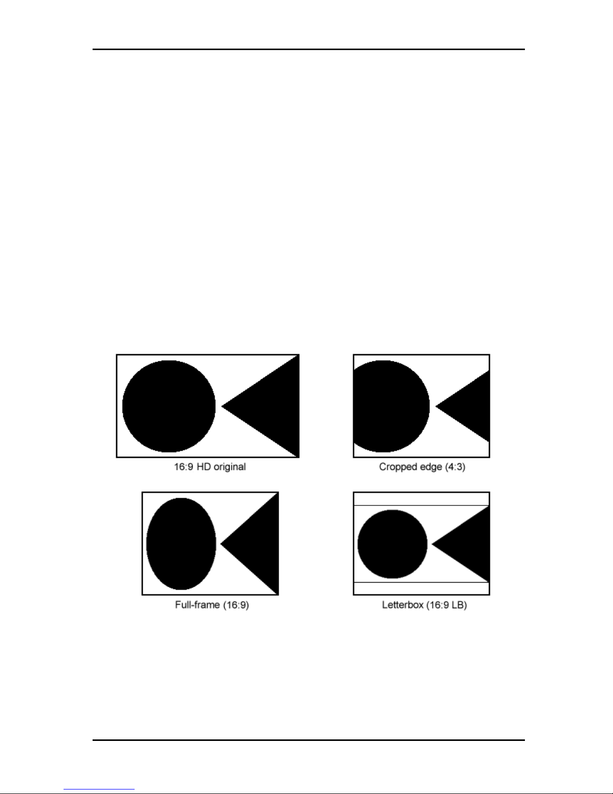
The following assumes that the aspect ratio of the incoming HD is 16:9, and that the pictures
are such that objects are shown geometrically correct on a 16:9 monitor. The user must then
set the crop and aspect ratio of the output and the illustration below shows the options
available. The figure assumes a 4:3 monitor that ignores the WideScreen Signaling bits
(WSS bits can be inserted automatically according to the selected aspect ratio, or they can
be turned off or replaced by a user selected value. See chapter 3.11 for details.) Had the
monitor in the example processed WSS bits, the full-frame picture in the lower left would’ve
been internally converted and shown letterboxed to preserve picture geometry. The cropped
edge 4:3 and letterboxed 16:9 options should normally only be used for 4:3 monitor.
Figure 3: Picture cropping and geometry options
3.6 Frame synchronizer
The frame synchronizer consists of a frame store buffer and some control logic. The frame
store buffer can store up to 8 SD frames. When the input is an HD source to be converted to
SD, the frame synchronizer is placed after the Scaling block. When the input is SD, the frame
Page 12

DWC-HD Rev. 5
nevion.com | 12
synchronizer is placed directly after the De-glitcher block. The control logic sets the frame
synchronizer in different modes of operation based on the presence of a sync input.
3.6.1 Frame Sync mode
If a sync input (B&B or Tri-level) is present, the frame synchronizer will output a signal that
has a delay relative to this signal. Two parameters can be set; output phase delay and
minimum delay.
The output phase delay can be positive or negative and sets the difference between the
phase of the sync input and the video output.
The minimum delay sets the minimum delay between video output and video input. The
actual delay can be larger than the minimum delay (hence the name), because the card must
also adjust the phase relative to the sync input.
The user may set the minimum delay up to 7 frames.
Example: The HD-SDI input signal is 12 lines delayed to a tri-level input signal. The minimum
delay is set to 1 frame, 0 lines and 0 samples. The output phase delay is set to 5 samples.
The actual delay between the input video and the output video will be 2 frames and 5
samples.
If video input disappears
Given that stable SDI input and sync input both exists: If the SDI input disappears, and Video
in and Processed video out are set to Auto, the board will hold on to the current input whilst
frame freezing for a time set by Hold time in Video in. The board will then select the next
input in the prioritized list. If that input is the internal video generator, the pattern selected in
Video generator will be output. Defaults are optical input as first priority, then electrical, and
finally fallback to Black video, with a Hold time of 3 seconds.
Note that input selection can be based on several rules, of which only Loss of signal (los) is
based on a status that can be checked for both inputs at the same time. This means that for
Los a direct jump from priority 1 to priority 3 is possible (in one Hold time period, because
priority 2 can be checked at the same time as priority 1), while the other rules require one
Hold time period for each jump between priority levels. It the board only has one physical
input in use, it is therefore recommended to set Video generator as the second priority.
If the SDI signal disappears and mode is set to manual in one or both of Video in and
processed video out, the effect will be that the board can frame freeze but will never switch to
another video input, including the fallback generator.
If video input reappears
Given stable sync input, the video will reappear after a user specified time of locked video.
This Lock time (in Video in) defaults to 3 seconds.
If sync input disappears
Given that stable SDI input and sync input exists: If the sync signal disappears, the board will
act as in frame delay mode, see Chapter 3.6.2.
NOTE: This will result in a frame roll as the delay changes.
If sync input reappears
Given that a stable SDI input exists: If the sync signal reappears the delay mode will change
back to Frame Sync mode. Hence the internal clock will be locked to the sync signal and the
delay will change again.
NOTE: This will result in a frame roll as the delay changes.
If both signals disappears
Page 13

DWC-HD Rev. 5
nevion.com | 13
The picture will first freeze for a user specified time (Hold time in Video in), and then possibly
(See section “If video input disappears” above) go to a fallback generator. The output is now
referenced to the local clock source. However, this clock source will be kept within 1 ppm of
the last sync source.
3.6.2 Frame delay mode
In this mode a sync signal is not present. The delay set is then directly related to the
incoming video. 1 frame and 1 line delay means that the output will be 1 frame and 1 line
delayed version of the input.
If video signal disappears
The picture will first freeze for a user specified time (Hold time in Video in), and then possibly
(See section “If video input disappear” under Frame sync mode above) go to a fallback
generator. The output is now referenced to the local clock source. However, this clock source
will be kept within 1 ppm of the last video source.
If video signal reappears
The video output will reappear after a user specified time of locked video. This Lock time (in
Video in) defaults to 3 seconds. The delay will now be the same as before loosing input.
NOTE: This may cause a frame roll.
If a sync input appears
Given that a stable SDI input exists: If a sync signal appears the delay mode will change to
Frame Sync mode, see Chapter 3.6.1. Hence the internal clock will be locked to the sync
signal and the delay will once again change.
NOTE: This will result in a frame roll as the delay changes.
3.7 Video generator
The video generator can produce different simple signals: Color bar, Check field and flat
field.
The flat field option allows the user to specify any combination of luma and chroma values, or
to select a predefined color from the following list:
- Black
- White
- Yellow
- Cyan
- Green
- Magenta
- Red
- Blue
In normal operation (as a fallback generator), the video generator will take its video standard
setting from the last lockable video input seen by the board. To enable the board to act as a
standalone and user configurable video generator, the video generator must be either set as
the first priority input when Mode is auto, or selected manually by setting Mode to Video
generator. Both settings are done in Processed video out. This will override any video input
but the generator signal will still be locked to the sync or SDI inputs, if present. For true
standalone generator operation, the inputs should be removed. Available video standards
are 486/25i and 576/25i.
Page 14

DWC-HD Rev. 5
nevion.com | 14
3.8 Video processing block
The video processing block consists of a gain and offset adjustment, and a video payload
legalizer.
3.8.1 Gain and offset
The gain and offset adjustment is done separately on the Y, Cb and Cr samples.
Range Gyda
Luma gain
0 – 32767 (0-4x, 1x = 8192)
Chroma gain
0 – 32767 (0-4x, 1x = 8192)
Luma offset (gain =1)
-4095 – 4095
(-511.75 – 511.75 in sample values)
Chroma offset (gain = 1)
-2047 – 2047
(-255.75 – 255.75 in sample values)
3.8.2 Video payload legalizer
The legalizer hard clips the upper and lower limit of the video payload. With the legalizer
enabled the limits are:
Upper limit
Luma:
3ACh
Chroma:
3C0h
Lower limit
Luma:
040h
Chroma:
040h
With the legalizer disabled, the video processing block hard clips both luma and chroma to
3FBh and 004h.
3.9 EDH processing block
If enabled, the EDH processing block extracts the EDH package from the video, updates the
EDH flags according to SMPTE RP165 and inserts the EDH package into the ancillary data
of the video.
If disabled, The EDH processing block only reads, process and report the EDH package
without changing it in video stream.
3.10 Video output selection
The board has four digital outputs and group of three analog outputs. The four digital outputs
are organized as two pairs, each consisting of an inverting and a non-inverting output. Each
pair and the analog group can take their signal directly from the re-clocker or from the output
of the processing unit. In Gyda the direct paths are labeled Through and the processing
paths are labeled Processed.
3.11 Video DAC
The video DAC has three configurable outputs, with the following combinations available:
- CVBS/CVBS/CVBS
- CVBS/Y/C
- Y/Pb/Pr
- R/G/B
This setting only applies to SD video. When HD video is routed to the video DAC, the output
will always be YPbPr. For CVBS and S-Video the following modulations are available:
- PAL B/G
- NTSC
Page 15

DWC-HD Rev. 5
nevion.com | 15
- PAL M
- PAL N
The board can handle 50Hz-based input signals as well as 60Hz-based with and without
pulldown, but can’t convert a 50Hz-based input to a 60Hz-based output and vice versa. The
modulation setting is therefore split in two, one to select between NTSC and PAL M output
for 60Hz-based sources, and one to select between PAL B/G and PAL N for 50Hz-based
sources.
It is also possible to turn black setup (“pedestal”) on or off. This setting only applies to NTSC.
PAL Wide Screen Signaling (WSS) is also supported, and while the HD input is always 16:9,
SD inputs can have value already embedded. The user can select to strip off any existing
WSS information by setting mode to Off, or to override the current WSS value by setting
mode to On and specifying a new value, or set the mode to Auto. When input is HD, the Auto
mode will insert WSS data according to the selected aspect ratio in the scaler block. When
the input is SD, the Auto mode will signal 4:3 or 16:9 based on the aspect ratio bit in SMPTE
352M byte 3, or turn WSS off if no SMPTE 352M packages are available.
When specifying WSS values, the user should observe that the WSS value is really a 14-bit
number with other information besides just aspect ratio. Aspect ratio is contained in the lower
4 bits, and the table below covers only those bits.
WSS value
Aspect ratio
Picture placement
Active lines
0+8=8
4:3
Full
576
1+0=1
14:9
Letterbox centre
504
2+0=2
14:9
Letterbox top
504
3+8=11
16:9
Letterbox centre
430
4+0=4
16:9
Letterbox top
430
5+8=13
>16:9
Letterbox deeper than 16:9
undefined
6+8=14
14:9
Full-height 4:3, framed to be “14:9-safe”
576
7+0=7
16:9
Full-height 16:9 (anamorphic)
576
Note the occasional “+8” in the first column above. It stems from the fourth aspect ratio bit, a
parity bit over the first three.
3.12 Audio overview
Figure 4: Audio function block
Page 16

DWC-HD Rev. 5
nevion.com | 16
3.13 Audio de-embedder
The Audio de-embedder extracts all audio embedded in the video stream. The de-embedder
is always enabled when the input is HD. When the input is SD and the board operates as an
SD frame synchronizer, embedding can be globally disabled. The effect is to leave the SDI
stream unaltered, except for repeated or removed video frames.
3.14 Audio delay
An audio delay can be specified relative to the video output. It is situated before the audio
cross point matrix and is common for all de-embedded channels. The audio delay is
specified in terms of 48 kHz audio samples, and can be set to positive or negative values.
NOTE: As the audio delay is relative to the video output it is possible to specify an audio
delay that will actually be a negative delay, i.e. ask that the sound is sent from the card
before it is received. This will obviously cause audio errors.
3.15 Audio cross point matrix
The audio cross point matrix is a 10x10 cross point with inputs and outputs as shown in
Figure 4. The 8 de-embedded channels, a 1 kHz sine and “black sound” are selectable
inputs. “Black sound” is explained in chapter 3.1. The outputs of the cross points are 8 stereo
channels for re-embedding, one analog audio output and one AES output.
3.16 Audio fallback options
The 10 output channels from the cross point matrix have configurable fallbacks, used when
their corresponding matrix inputs are missing. A common fallback setting is used for all eight
re-embedder channels, whereas the audio DAC channel and AES out have their own
independent fallback settings. The priorities can be selected between matrix (being the
selected channel in the cross point matrix) or the internally generated sine or black sound.
3.17 Audio generator
The stereo audio generator is available as an input to the audio cross point matrix, and as a
fallback option. There are therefore three slightly different ways to select the generator:
select it in the matrix directly, select it as the first priority under audio fallback, or to set it as
second priority behind a missing input.
The generator signal is a high purity 1 kHz sine wave with a 250ms interruption on the left
channel every 3 seconds. The audio level may be set to one of two standards. The two
levels are -18 dBFS and -20 dBFS. These two levels correspond to EBU R68 and SMPTE
RP155.
3.18 Audio processing block
The output of each stereo signal from the audio cross point matrix may be manipulated in the
audio processing block (LL, RR, LR, RL !LR, L!R, (L+R)/2, MS).
The stereo signals may be output in one of the following ways:
- LR, Left / Right
No change.
- RL, Right/ Left
Channels are swapped.
- LL, Left/ Left
Left channel is copied into the right channel.
- RR, Right/ Right
Right channel is copied into the left channel.
- !LR, ØLeft/ Right
The left channel is phase inverted.
- L!R, Left/ ØRight
The right channel is phase inverted.
- MM, (Left + Right)/2
The left and right channels are summed.
- MS, MS/AB
The left and right channels are converted from AB stereo
to MS stereo.
Page 17

DWC-HD Rev. 5
nevion.com | 17
3.19 Audio embedder
The audio embedder can be enabled/disabled per group. When a group to be embedded is
disabled the audio inside that group is removed.
A 24-bit audio signal uses the Extended Audio Data Packet for the 4 least significant bits. Not
all equipment can handle Extended Audio Data Packets correctly, so the option exists to
truncate all audio data to 20 bits. This setting is common for all embedder channels.
The insertion of Audio Control Packages can also be switched on and off. This setting is
also common for all embedder channels.
For SD input (i.e. operation as a frame synchronizer) the audio embedder can also be
switched off all together. In this state all audio embedded on the input signal is left
unchanged.
3.20 Analog audio output
The level of the analog audio output can be adjusted in GYDA. The minimum step is 0.5dB
(input will be rounded to nearest 0.5dB) and the range is from -95.5dBu to 24dBu. It is also
possible to mute the output completely.
Page 18

DWC-HD Rev. 5
nevion.com | 18
4 Configuration
4.1 DIP switch functions
The two sets of DIP switches are labeled with a number running from 1 to 15. The 16th DIP is
labeled OVR. Note that the left DIP switch of the horizontal DIP package is number 1. The
top DIP switch of the vertical DIP package is number 9. Default settings as delivered from
factory should be all DIPs in the Off position. The module will then be under Gyda control,
see description for DIP switch 16 below.
Table 1: DIP SWITCH FUNCTIONS
Switch #
Function name
Function DIPs
Comment
1
SDI OUT 1
+
Video DAC out
Off: processed mode
On: through mode
In through mode the
video goes through a
re-clocker only, and
the video DAC
output will also be
HD (always YPbPr).
2
SDI OUT 2
Off: processed mode
On: through mode
In through mode the
video goes through a
re-clocker only.
3 - 4
Aspect ratio
DIP[3 4] = [Off Off] => 16:9
DIP[3 4] = [Off On] => 4:3
DIP[3 4] = [On Off] => 16:9 LB
DIP[3 4] = [On On] => Previous
setting preserved
These 2 DIPs
choose aspect ratio
for down-converted
video.
“Previous setting
preserved”: With
DIPs in this position
before the module is
booted into manual
mode; the module
will keep the
previous value set by
Gyda.
5 - 6
SD video DAC
format
DIP[5 6] = [Off Off] => CVBS
DIP[5 6] = [Off On] => YPbPr
DIP[5 6] = [On Off] => SVideo
DIP[5 6] = [On On] => RGB
These two DIPs
choose video DAC
output format for SD
output. Analog HD is
always YPbPr.
7
SD video DAC
modulation
Off: PAL B/G + NTSC
On: PAL N + PAL M
Selection between
PAL B/G and NTSC
or PAL M and PAL N
is automatic, based
on video input.
8
Black setup
disable
Off: Black setup for NTSC
On: No black setup
For NTSC only.
9 Input priority Off: Optical input has priority
On: Electrical input has priority
This switch has no
effect for boards
without the optical
input (-R option).
10 - 11
Audio DAC and
AES group
DIP[10 11] = [Off Off] => Gr1
DIP[10 11] = [Off On] => Gr2
DIP[10 11] = [On Off] => Gr3
DIP[10 11] = [On On] => Gr4
The 2 first of these 4
DIPS select one of
the de-embedded
groups. The next two
Page 19

DWC-HD Rev. 5
nevion.com | 19
Switch #
Function name
Function DIPs
Comment
12
Audio DAC
channel
Off: Ch1
On: Ch2
(from selected group)
DIPs select a
channel pair (within
this group) for the
audio DAC and one
for the AES output,
respectively.
13
AES channel
Off: Ch1
On: Ch2
(from selected group)
14
AES/Dlink
Off: AES3 out on AES output
On: Data link out on AES output
The two slide
switches on the
bottom side of the
board must also be
switched.
See ch. 4.2.2below.
15
RESET
Off: Use values preset by GYDA
On: RESET to factory defaults
This DIP is only read
during boot. The
board will not start
when DIP 16 and
this DIP are both set
to On. After returning
the DIP to normal
position, the card
must be restarted
and kept powered for
a minimum of 10s to
complete the reset.
The reset will only
affect settings not
pertaining to DIPs
and the rotary
switch.
16
OVR
Off: GYDA mode
On: Manual mode
This DIP is only read
at power up.
OVR is short term for
GYDA override.
4.2 FACTORY reset function
A factory reset is a 3 step process:
- Set DIP 15 to ‘on’ and boot the card.
- Remove power and set the reset switch back to normal position (‘off’)
- Power up card once again. The operation of the card will immediately reflect the freshly
loaded default settings. However, the card must be kept powered for at least 10
seconds to ensure that these settings are stored locally to be retrieved again at the
next start-up. The cards operational environment must also be kept static during those
10 seconds (i.e. no change in incoming video standard, no commands issued). Failing
to meet this requirement could result in an incomplete reset and require the user to
restart the factory reset sequence.
4.2.1 Rotary switch and push buttons
The rotary switch, labeled DLY, adjusts the phase delay from -5 to +4 video lines. It is only
functional when a sync signal, black & burst or tri-level, is present at the sync input. The
rotary switch is accessible from the board front.
Page 20

DWC-HD Rev. 5
nevion.com | 20
The push buttons, labeled INC and DEC, are used to fine adjust the phase delay by samples.
It can adjust ±½ video line for the current video standard (or the last video standard the
board was able to lock to). Pressing a button and keeping it pressed will accelerate the
change. The LED adjacent to the button will flash for a short period of time when the end of
the adjustment range has been reached. Pressing both buttons at the same time will return
to the middle of the adjustment range, and the board will acknowledge by flashing the INPUT
and SYNC LEDs simultaneously.
4.2.2 Slide switches
The two switches at the top of the module (rear side) switch between AES out and Data out.
It DC couples the output signal when in DATA out mode, and AC couples the signal when in
AES mode.
Note that to enable Data link output on the AES connector it is also necessary to
set DIP 8 to the Off position when the board is in Manual mode (DIP 16 = On), or
when the board is in Gyda mode (DIP 16 = Off), to select Data link over AES
output in Gyda. Slide switches moved to the right routes out AES.
The switch on the left card edge switches between backplane sync input and Flashlink
distributed sync (Future feature upgrade of Flashlink frame). Switch moved up routes the
backplane sync to the card.
Figure 5: The figure shows a bottom view component printout of the board. Note the location
of the slide-switches.
4.3 GYDA mode
All functions of the card can be controlled through the GYDA control system. The GYDA
interface has an information page and a configuration page.
4.3.1 Information page
The information page shows a dynamic block-diagram of the board and some additional
information text. The block diagram updates with the board status, showing selected input
signal, missing signals (by red crosses over the appropriate signal lines) and signal routing
(by graphic switches). It also shows the audio matrix selections that have been made in the
configuration page.
Note that if a stereo pair of embedded audio is missing, the user will still be
allowed to select that pair from the audio matrix. The output will however go to
the fallback position immediately. A missing stereo pair will be shown in the
block-diagram as a red cross over the appropriate matrix input line.
Page 21

DWC-HD Rev. 5
nevion.com | 21
The text on the information page gives information about functionality not displayed on the
dynamic block diagram.
The video delay represents the actual delay between input and output video.
The audio de-embedders 1-4 show the state of the audio control package for their associated
audio group de-embedded from the input stream.
The audio embedders 1-4 show the state of the audio control package and the audio bit
depth for their associated audio group embedded in the output stream.
Embedded UART shows the data rate of the data link embedded in the audio control
packages on the incoming signal.
4.3.2 Configuration page
The different configuration possibilities are explained in Chapter 3, under the corresponding
blocks or functions.
Page 22

DWC-HD Rev. 5
nevion.com | 22
5 Connections
Figure 6: DWC-HD-DMUX-C1
The backplane for the DWC-HD-DMUX is labeled DWC-HD-DMUX-C1. The table below
shows the connectors and their functions.
Function
Label
Connector type
HD/SD-SDI input
IN
BNC
HD/SD-SDI output 1
O1
BNC
HD/SD-SDI output 2
O2
BNC
Analog video, Y/G/CVBS
Y/G/CVBS
BNC
Analog video, Pb/B/Y
PB/B/Y
BNC
Analog video, Pr/R/C
PR/R/C
BNC
Sync input
SYNC
BNC
Analog audio out left channel
AAL
WECO Audio connector
Positive
GND
Negative
Analog audio out left channel
AAR
WECO Audio connector
Positive
GND
Negative
AES out
AES
WECO Audio connector
Positive
GND
Negative
Optical input
OPT1
BSC-II (for SC input)
Page 23

DWC-HD Rev. 5
nevion.com | 23
6 Operation
6.1 Front panel LED indicators
Diode \ state
Red LED
Orange LED
Green LED
No light
Card status
PTC fuse has been
triggered or FPGA
loading has failed
FPGA
loading. If
more than a
few seconds:
DIPs 14+15
both set to the
‘On’ position,
or module not
programmed
Module is OK
Module has no
power
SDI input
status
Video signal absent
Video signal
present but
card not able
to lock VCXO
Video input
signal in lock
Module not
programmed, or
DIPs 14+15 both
set to the ‘On’
position
Sync input
status
Sync signal absent
Sync signal
present but
card unable to
lock VCXO
B&B or Tri-
level sync in
lock
Module not
programmed, or
DIPs 14+15 both
set to the ‘On’
position
Audio input
status
No audio
embedded in
incoming video
One, two or
three audio
groups
embedded in
incoming
video
4 audio
groups
embedded in
incoming
video
Module not
programmed, or
DIPs 14+15 both
set to the ‘On’
position
6.2 RS422 commands
6.2.1 FLP4.0 required commands
Block
Blk# Commands
Example
Response
Control
- - ?
?
product name\
SW rev n.m\
FW rev r.s\
protocol ver 4.0\
Hello command.
Note 1: No other commands will be
available until the card has received
this hello.
Note 2: This command will also
enable checksums.
Note 3: Cards are designed to be
hot-swappable. To sync with the start
of a new command, the cards will
wait for a <lf> character before
looking for a valid command.
conf 0 - conf 0 *too long to list*
Configuration settings
Retrieves the card's configurable
settings. Each addressable block is
represented by a single line. Dynamic
status may be included in response,
but is usually reported in info only.
- - info
info
*too long to list*
Dynamic status info
Blocks with static settings only will
usually not be included, see conf
Page 24

DWC-HD Rev. 5
nevion.com | 24
Block
Blk# Commands
Example
Response
Control
above.
- - chk off
chk off
ok
Checksum off
If issued twice in succession, this
command will disable checksums.
Note: Responses will still have the
checksums appended.
NOTE1:? command turns the
checksum on again
- - locate on <seconds>
locate off
locate on 3
locate off
ok
Card locator
This command will cause all the
LEDs to flash for a user specified
number of seconds. If omitted, the
value <seconds> will be set to a
default of 120 seconds. The flashing
can be terminated at any time with
locate off.
- - address
address
address <address>
Card address
This command will force the module
to check and update its current rack
and slot address. This is normally
only done at start-up.
- - filename
filename dwchddmux-
0-105.ffw
<name>'.'<extensio
n>
Firmware update
The <name> part must match the
card's hardware and include a
revision number, and the extension
must be either 'ffw' for FPGA
firmware or 'mfw' for microcontroller
firmware. After running this command
the board will be ready to receive its
new firmware in Intel-hex format.
- - fin
fin
ok
Finalize
Finalize the programming of the
microcontroller. See description of
the uC boot loader (separate
document).
misc 0 -
NOT AVAILABLE BY
COMMAND.
ONLY FOUND in conf
0
prog | fin
' ' | ovr
Misc info
prog if the card is freshly
programmed by the boot loader and
the program is still un-finalized. fin is
the normal condition.
ovr if DIP-switch 16 is set to the ON
position and the card is under DIPswitch control.
Note 1: The info part of misc has
additional functionality when locate is
used: locating <remaining seconds>.
This enables a visible countdown
clock in Gyda, but is not a required
part of FLP400.
Page 25

DWC-HD Rev. 5
nevion.com | 25
6.2.2 Normal control blocks
Block
Blk# Commands
Example
Response
Control
pin 0 on | off
pin 0 on
pin 0 off
cd | ncd
Pin diode for optical input. No control
available, except to turn power to the
pin diode on or off. The info string
reports carry detect or not carry
detect.
ceq 0 -
ceq 0
cd | ncd
Cable equalizer for electrical input.
No control; only used to report carry
detect or not carry detect.
cho 0 pri <k> |
pri <k> <l> |
pri <k> <l> <m>
pos man <k> |
pos auto
latch on |
latch off|
latch reset
rule lol |
rule los |
rule trse
t1 <hold_time>
t2 <lock_time>
cho 0 pri 0
cho pri 0 1
cho pri 10 2
cho 0 pos man 1
cho 0 pos auto
cho 0 latch on
cho 0 latch off
cho 0 latch reset
cho 0 rule lol
cho 0 rule los
cho 0 rule trse
cho 0 t1 1000
cho 0 t2 1000
size 3 pri k,l,m auto
latch
<latch_status> t1
<hold time> t2
<lock time> <rule>
size 3 pri k,l,m man
m latch
<latch_status> t1
<hold time> t2
<lock time> <rule>
Video input select
pri: a prioritized list of inputs, used
when change-over is automatic. The
list can have 1, 2 or 3 entries, or
levels. Manual mode is effectively the
same as automatic mode with one
priority level only, but has its own
command.
0 = from optical input
1 = from electrical input
2 = generator (from cho 1)
latch: <latch_status> can be either
on or off and selects if the changeover is latching or not, used when
change-over is automatic. Latch on
means that if we've lost our main
source and moved on to a lower
priority level, we'll not search to see if
the higher pris will reappear.
rule: <rule> can be either los, lol or
trse, which means loss off signal,
loss of lock, and timing reference
signal error. This determines what
triggers an automatic change-over.
t1 and t2: change-over doesn't
happen immediately, as a precaution
against glitches and unstable signals.
The timers t1 and t2 let the user
decide how long (in ms) we will cling
on to a missing input before we
consider it gone and move on to the
next pri level, and how long an input
with a higher priority should be
present before we consider it
repaired and switch back,
respectively.
Note 1: the latch setting only applies
to rule los.
Note 2: the card change back to
physical inputs from generators
regardless
of latch setting. As a side
note, this means that t2 is important
even when rule=lol and/or latch is on.
Note 3: If we have selected rule=lol
and a 3-level pri list with two physical
inputs on top and a generator at the
bottom and we're in generator mode
(lost both physical inputs) and both
Page 26

DWC-HD Rev. 5
nevion.com | 26
Block
Blk# Commands
Example
Response
Control
physical inputs reappear at more or
less the same time, which physical
input will be chosen is unpredictable.
This again due to having one
reclocker only and having to hunt for
a valid input in the background while
the generator is still selected.
cho 1 pri <k> |
pri <k> <l>
pos man <k> |
pos auto
cho 1 pri 0
cho 1 pri 0 1
cho 1 pos man 1
size 3 pri k,l auto
size 3 pri k,l man m
Video fallback setting
Second video change-over. This cho
is a slave of cho 0, in the sense that it
has no latch, t1, t2 or rule settings of
its own. It has a generator input that
must be set up separately and that
allows a switch to an internal video
generator.
0 = from cho 0
1 = from video generator, vgen 0
2 = kill
Note: manual mode is the same as
automatic mode with a priority list
with only one priority level.
cho 2-
11
pri <k> |
pri <k> <l>
cho 2 pri 1
cho 5 pri 0 2
size 4 pri k,l
Audio fallback setting
Audio change-over blocks, one cho
per audio output from the audio
matrix, mtx 0. No other settings but
the priority list.
0 = from audio matrix
1 = sine
2 = black
3 = kill
Note: Only generators (pri 1, 2 or 3)
are allowed to be set as first and only
priority.
cho
12
pri <k> |
pri <k> <l>
cho 12 pri 1
cho 12 pri 0 2
size 4 pri k,l
Audio common fallback setting
A short-cut to set change-over’s 2-11
all at once. Will of course not report
anything in info, that's left to the
individual cho blocks.
cho 13 pos man <k> cho 13 pos man 0
cho 13 pos man 1
size 2 man k
AES output select
This change over has only manual
mode and works as a simple 2:1
switch.
0: AES is selected
1: Embedded UART is selected
cho
14
pos man <k>
cho 14 pos man 0
cho 14 pos man 1
size 2 man k
EDH insert select
This change over has only manual
mode and works as a simple 2:1
switch.
0: EDH off
1: EDH on
cho
15
pos man <k>
cho 15 pos man 0
cho 15 pos man 1
size 2 man k
SDO 0 output select
This change over has only manual
mode and works as a simple 2:1
switch.
0: Through mode (re-clocked only)
1: Processed mode (from FPGA)
cho
16
pos man <k>
cho 16 pos man 0
cho 16 pos man 1
size 2 man k
SDO 1 output select
This change over has only manual
mode and works as a simple 2:1
Page 27

DWC-HD Rev. 5
nevion.com | 27
Block
Blk# Commands
Example
Response
Control
switch.
0: Through mode (re-clocked only)
1: Processed mode (from FPGA)
cho 17 pos man <k> cho 17 pos man 0
cho 17 pos man 1
size 2 man k
Video DAC output select
This change over has only manual
mode and works as a simple 2:1
switch.
0: Through mode (re-clocked only)
1: Processed mode (from FPGA)
cho
18
pos man <k>
cho 18 pos man 0
cho 18 pos man 1
size 2 man k
Audio embedding enable for SD
This change over has only manual
mode and works as a simple 2:1
switch.
0: embedding off (Audio embedded
on input signal left untouched)
1: Embedding on
cho
19
pos man <k>
cho 19 pos man 0
cho 19 pos man 1
size 2 man k
Color space conversion on/off
0: no conversion
1: color space conversion from HD to
SD
rcl 0 -
rcl 0
lock | lol
Reclocker. No control; only used to
report lock status.
emb
0-3
en | dis
acp ( on | off )
use24 ( on | off )
del (off | (on <del12>
<del34>))
emb 0 en
emb 2 dis
emb 1 acp on
emb 3 acp off
emb 1 use24 on
emb 2 use24 off
emb 0 del off
emb 2 del on 54 -432
(en | dis) use24 (on
| off) acp (on | off)
del (off | (on
<del12> <del34>))
Audio embedder block
en/dis: Enables or disables the
embedding of the group into the
ancillary area.
acp on/off: This is valid only for SD
and enables the audio control
package.
use24 on/off: This is only valid for
SD and selects between 24bit and
20bit sound.
del off/on delay12 delay34: For
each of the embedder groups the
delay bits for ch1+2 and for ch3+4
can be inserted into the ACP. The
delay value can be positive and
negative and is put directly into the
ACP as it is written.
Note: To set both delays to 0 would
be the same as turning the delays off.
The response reflects this.
demb
0-3 - demb 0
demb 2
grp k en
Audio de-embedders
one permanently assigned to each
incoming group, always enabled. No
control available.
scale 0 asp <aspect_ratio> out
<video_standard>
asp <aspect>
Set down-converter aspect ratio.
Supported aspect ratios at the
moment are “16/9”, “16/9lb” and
“4/3”. Video standard output from the
scaler block is also included (576/25i
or 486/29i, selected based on
incoming video standard). Video
standard information is duplicated in
info.
Note: converter is always present
and active. The user must use cho
Page 28

DWC-HD Rev. 5
nevion.com | 28
Block
Blk# Commands
Example
Response
Control
15-17 to select between
processed/unprocessed output
vprc 0 lglz on |
lglz off
(y | cb | cr) <gain>
<offset>
vprc 0 lglz on
vprc 0 lglz off
vprc 0 y 8192 0
vprc 0 cb 2000 0
vprc 0 cr 1000 1000
Video processing block
Gain and offset are both signed fixed
point numbers. Gain is in 2.13format, while offset for Y and the
chroma channels are given in 10.2
and 9.2 respectively.
Gain range is 0 – 32767, Gain
=0x
= 0,
Gain
=1x
= 8192, Gain
=4x
= 32767
Luma Offset range is -4095 – 4095,
Offset
=0
= 0
Chroma Offset range is -2047 –
2047, Offset=0 = 0
sync
0 - sync 0
'lol' | ('lock' ('trilvl' |
'bb' | 'sdi') )
Sync block
Frequenc
y reference for video output.
Status only, no commands available.
dly 0 <frames>frms
<lines>lines
<samples>sps
dly 0 2frms
dly 0 2lines 30sps
dly 0 0frms 50sps
dly 0 0frms 3lines
50sps
'tgt' <frames> frms
<lines> lines
<samples> sps
Video delay
This sets the minimum video delay of
the card.
In info this block reports back the
current delay in nanoseconds. This
will vary with the incoming video
standard.
dly 1 <audio_samples>sps
dly 1 -30sps
'tgt'
<audio_samples>
sps
audio delay
The audio delay is given in audio
samples. Audio delay is always given
relative to video.
dly 2 <lines>lines
<samples>sps
dly 2 1lines -30sps
'phase' <lines>
lines <samples>
sps
Video phase
If lines != 0 the resulting phase will
vary with incoming video standard,
see dly 0 above.
vgen
0
cbar |
chkfield |
white |
yellow |
cyan |
green |
magenta |
red |
blue |
black
flat <Y> <Cb> <Cr>
video
<lns>/<rate><scan>
wss (off | (on
<wss_val>) )
vgen 0 cbar
vgen 0 flat 200 0 100
vgen 0 video 576/25i
vgen 0 video 486/29i
vgen 0 wss auto
vgen 0 wss on 7
video
<lns>/<rate><scan
> wss ( auto| off | (
on <wss_value> ) )
(cbar | chkfield |
white | yellow |
cyan | green |
magenta | red |
blue | black | (flat
<Y> <Cb> <Cr>) )
Internal video generator.
The video generator will be activated
in two different ways: If selected as a
fallback option the generator will
generate the selected pattern when
the other input(s) are missing, and
then use the video settings from the
last external source present. It can
also be selected as the main input in
cho 1, in which case its own video
settings will also be used.
vdac
0
cvbs |
ypbpr |
rgb |
svideo |
palbg |
palm |
paln |
ntsc |
bsetup (on | off ) |
wss (auto | off | (on
vdac 0 fmt ( cvbs |
ypbpr | rgb | svideo
) mod ( palbg | paln
) ( ntsc | palm )
bsetup ( on | off )
wss ( auto (on | off )
| on | off )
Video DAC
The module can handle 50Hz- and
60Hz-based sources, but can’t
convert video material between these
time bases. The user must therefore
select two modulations, one for
50Hz-based sources and one for
60Hz-based sources.
The (on | off) immediately following
the wss auto is a status telling if the
Page 29

DWC-HD Rev. 5
nevion.com | 29
Block
Blk# Commands
Example
Response
Control
<wss_val>) )
WSS bits are currently in use.
edh 0 msk <24b_mask>
reset
edh 0 msk 0xFE00
edh 0 reset
msk <24b_mask>
Error detection and handling
Error counting. The count itself is
reported in info. Errors can be
masked off and not counted; this is
the purpose of the mask. The counter
itself is 16b and will wrap around, but
can also be reset by issuing reset.
mtx 0 <i1> <o1> ...<iN>
<oN>
<i1>
<o1>,<o2>,...<oN>
<i1> <o1> - <o2>
..or the above
combined
mtx 0 0 2 1 4 5 5
mtx 0 0 0, 1 1, 2 2
mtx 0 0 0-9
mtx 0 0 0 1 1 2 2-9
size M:N i1 i2 i3...
iN
Audio matrix
mtx 0 (size 10:10) controls the audio
matrix; outputs 0-7 are embedded
sound, 8=adac and 9=AES.
Note: Any combination of the three
basic commands are allowed, for
instance the following command to
set up a 10x10 audio matrix in a
single line:
mtx 3 1 1 2 2 3 0,3-9
=> mtx 3 size 10:10 3 1 2 3 3 3 3 3 3
3
agen 0 lvl <sine_level>cBFS agen lvl -180
agen lvl -200
sine 1kHz lvl
<sine_level>cBFS
Audio generator
The amplitude of the generated sine
that can be chosen as fallback in
audio change-overs. Legal values are
-180cBFS or -200cBFS (centiBel
referred to full scale output). Units
are optional, but if included must be
written as cBFS (case sensitive).
aprc
0-9
lr |
rl |
ll |
rr |
nlr |
lnr |
mm |
ms
aprc 0 lr
aprc 3 ll
aprc 9 mm
lr |
rl |
ll |
rr |
nlr |
lnr |
mm |
ms
Audio processing
one block for each output from cho 2-
11. Outputs 8+9 are adac and AES,
the lower 8 are routed to the
embedder. The meaning of the
commands are as follows:
lr = Normal
rl = Channel swapped
ll = Left channel to both output
channels
rr = Right channel to both output
channels
nlr = Left channel phase inverted
lnr = Right channel phase inverted
mm = Mono, both channels = (r+l)/2
ms = Mono/stereo, m=(l+r)/2, s=(l-r)/2
ablk 0 mute ( on | off )
lvl <level>
ablk 0 mute on
ablk 0 mute off
ablk 0 lvl -500
ablk 0 lvl 30
dac lvl <level>cBu
mute
<mute_status>
Audio DAC control
This word dac identifies this audio
block as a DAC. The outputs can be
muted, <mute_status> given as on or
off, and the output level can be set in
cBu (tenth dBu). Units are optional, if
included must be written as cBu
(case sensitive).
Note 1: The lvl and mute are
independent, so that the card will
remember the lvl setting (and change
lvl setting) while muted.
Note 2: The resolution of the lvl
control is 0.5dB but the card will
perform correct rounding to nearest
legal value and report the resulting
setting. Legal input range is [-
Page 30

DWC-HD Rev. 5
nevion.com | 30
Block
Blk# Commands
Example
Response
Control
957cBu, 247cBu], representing the
range [-95.5dBu, 24.5dBu].
uart 0 - tx
The embedded data link, selectable
by cho 13. No control possible, the
word tx indicates that this is a
transceiver only.
Uart info reports link status: los (loss
of signal), raw, or the speed of the
embedded link (example:
115200/8/n/1).
6.2.3 Commands intended for debug/lab use only
Block
Blk# Commands
example
Response
Control
spir - <address>
spir 0x0004
Read a single word (or byte) from a
SPI registers to check register status.
Addressing is 16b and most
significant nibble determines which
chip. These are the address ranges:
0x0000 – 0x0fff : audio DAC
0x1000 – 0x1fff : FPGA
0x2000 – 0x2fff : flash
0x3000 – 0x3fff : deserializer
0x4000 – 0x4fff : serializer
0x5000 – 0x5fff : shift register (for
LEDs)
0x6000 – 0x7fff : video DAC
Note: The video DAC is actually
using I2C, but the addresses are
mapped into the SPI address range.
spiw - <address> <data>
spiw 0x0004 0x2c
With the same address ranges as for
spir above, this command allows
single SPI registers to be modified.
Modifying SPI registers in the flash
area is strongly discouraged!
Page 31

DWC-HD Rev. 5
nevion.com | 31
General environmental requirements for Nevion equipment
1.
The equipment will meet the guaranteed performance specification under the following
environmental conditions:
-
Operating room temperature range:
0°C to 45°C
-
Operating relative humidity range:
<90% (non-condensing)
2.
The equipment will operate without damage under the following environmental
conditions:
-
Temperature range:
-10°C to 55°C
-
Relative humidity range:
<95% (non-condensing)
Page 32

DWC-HD Rev. 5
nevion.com | 32
Product Warranty
The warranty terms and conditions for the product(s) covered by this manual follow the
General Sales Conditions by Nevion, which are available on the company web site:
www.nevion.com
Page 33

DWC-HD Rev. 5
nevion.com | 33
Appendix A Materials declaration and recycling information
A.1 Materials declaration
For product sold into China after 1st March 2007, we comply with the “Administrative
Measure on the Control of Pollution by Electronic Information Products”. In the first stage of
this legislation, content of six hazardous materials has to be declared. The table below
shows the required information.
組成名稱
Part Name
Toxic or hazardous substances and elements
鉛
Lead
(Pb)
汞
Mercury
(Hg)
镉
Cadmium
(Cd)
六价铬
Hexavalent
Chromium
(Cr(VI))
多溴联苯
Polybrominated
biphenyls
(PBB)
多溴二苯醚
Polybrominated
diphenyl ethers
(PBDE)
DWC-HD-DMUX O O O O O O
O: Indicates that this toxic or hazardous substance contained in all of the homogeneous materials for
this part is below the limit requirement in SJ/T11363-2006.
X: Indicates that this toxic or hazardous substance contained in at least one of the homogeneous
materials used for this part is above the limit requirement in SJ/T11363-2006.
This is indicated by the product marking:
A.2 Recycling information
Nevion provides assistance to customers and recyclers through our web site
http://www.nevion.com. Please contact Nevion’s Customer Support for assistance with
recycling if this site does not show the information you require.
Where it is not possible to return the product to Nevion or its agents for recycling, the
following general information may be of assistance:
− Before attempting disassembly, ensure the product is completely disconnected from
power and signal connections.
− All major parts are marked or labeled to show their material content.
− Depending on the date of manufacture, this product may contain lead in solder.
− Some circuit boards may contain battery-backed memory devices.
Page 34

Nevion Europe
P.O. Box 1020, 3204 Sandefjord, Norway – Tel: +47 33 48 99 99 – Fax: +47 33 48 99 98
www.nevion.com
EC Declaration of Conformity
MANUFACTURER
Nevion Europe AS
P.O. Box 1020, 3204 Sandefjord, Norway
AUTHORIZED REPRESENTATIVE
(Established within the EEA)
Not applicable
MODEL NUMBER(S)
DWC-HD-DMUX
DESCRIPTION
HD-SDI to SD-SDI Down-converter
DIRECTIVES this equipment complies with
LVD 73/23/EEC
EMC 2004/108/EEC
RoHS (EU Directive 2002/95/EC)
China RoHS
1
WEEE (EU Directive 2002/96/EC)
REACH
HARMONISED STANDARDS applied in order
to verify compliance with Directive(s)
EN 55103-1:1996
EN 55103-2:1996
TEST REPORTS ISSUED BY
Notified/Competent Body
Report no:
Nemko
E08463.00
TECHNICAL CONSTRUCTION FILE NO
Not applicable
YEAR WHICH THE CE-MARK WAS AFFIXED
2008
TEST AUTHORIZED SIGNATORY
MANUFACTURER
AUTHORIZED
REPRESENTATIVE
(Established within EEA)
Date of Issue
2008-06-16
Place of Issue
Not applicable Sandefjord, Norway
Name
Thomas Øhrbom
Position
QA Director, Nevion Europe
(authorized signature)
1
Administration on the Control of Pollution Caused by Electronic Information Products
 Loading...