

NEC MC-4532CD646EF-A10, MC-4532CD646EF-A80, MC-4532CD646PF-A10, MC-4532CD646PF-A80 Datasheet
DATA SHEET
MOS INTEGRATED CIRCUIT
MC-4532CD646
32M-WORD BY 64-BIT SYNCHRONOUS DYNAMIC RAM MODULE
UNBUFFERED TYPE
Description
The MC-4532CD646 is a 33,554,432 words by 64 bits synchronous dynamic RAM module on which 16 pieces of
128M SDRAM: µPD45128841 are assembled.
This module provides high density and large quantities of memory in a small space without utilizing the surfacemounting technology on the printed circuit board.
Decoupling capacitors are mounted on power supply line for noise reduction.
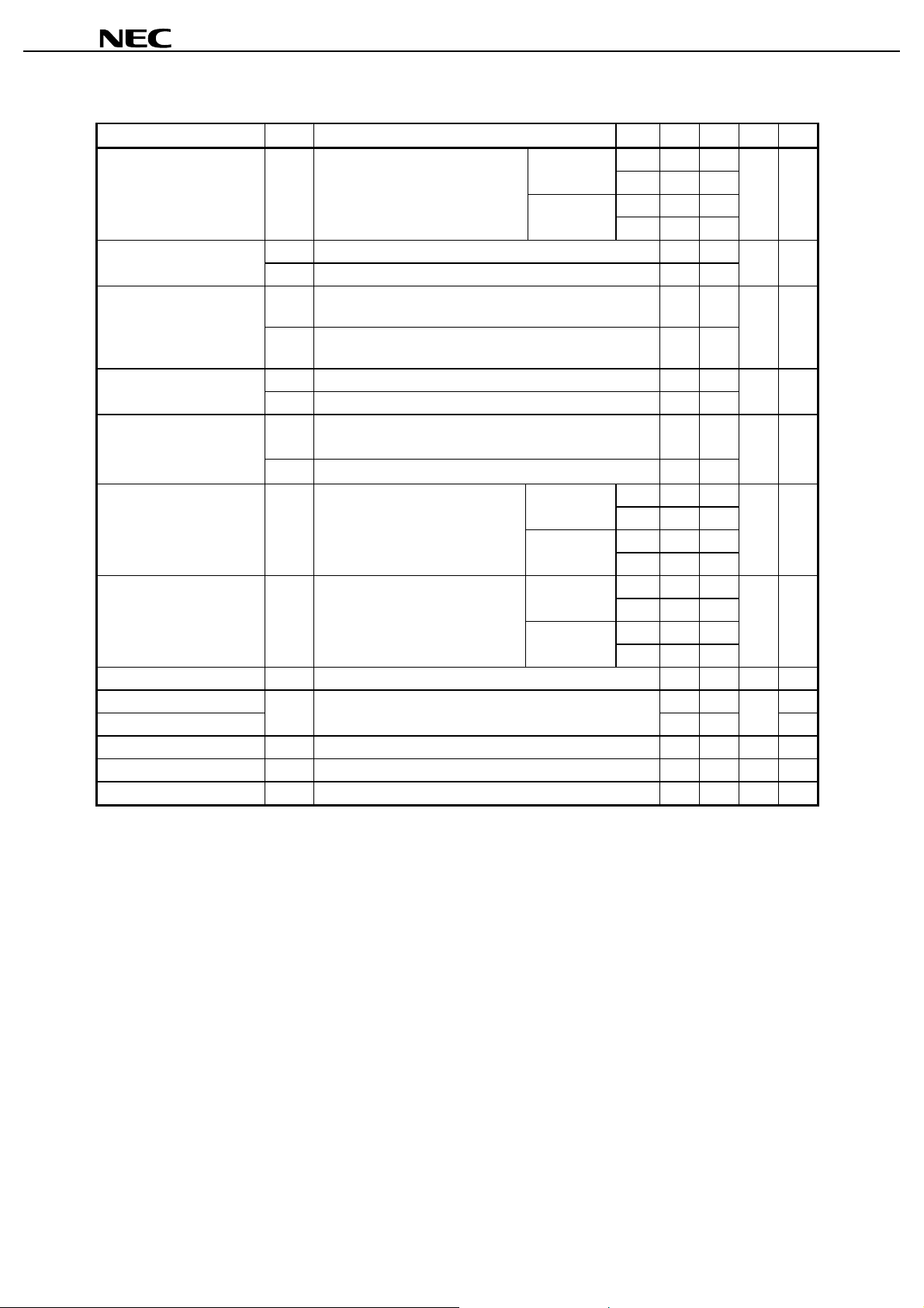
Features
• 33,554,432 words by 64 bits organization
• Clock frequency and access time from CLK
Part number /CAS latency Clock frequency
(MAX.)
MC-4532CD646EF-A80 CL = 3 125 MHz 6 ns
CL = 2 100 MHz 6 ns
MC-4532CD646EF-A10 CL = 3 100 MHz 6 ns
CL = 2 77 MHz 7 ns
★
★
MC-4532CD646PF-A80 CL = 3 125 MHz 6 ns
CL = 2 100 MHz 6 ns
MC-4532CD646PF-A10 CL = 3 100 MHz 6 ns
CL = 2 77 MHz 7 ns
• Fully Synchronous Dynamic RAM, with all signals referenced to a positive clock edge
• Pulsed interface
• Possible to assert random column address in every cycle
• Quad internal banks controlled by BA0 and BA1 (Bank Select)
• Programmable burst-length (1, 2, 4, 8 and full page)
• Programmable wrap sequence (Sequential / Interleave)
• Programmable /CAS latency (2, 3)
• Automatic precharge and controlled precharge
• CBR (Auto) refresh and self refresh
• All DQs have 10 Ω ±10 % of series resistor
• Single 3.3 V ± 0.3 V power supply
• LVTTL compatible
• 4,096 refresh cycles/64 ms
• Burst termination by Burst Stop command and Precharge command
• 168-pin dual in-line memory module (Pin pitch = 1.27 mm)
• Unbuffered type
• Serial PD
Access time from CLK
(MAX.)
The information in this document is subject to change without notice. Before using this document, please
confirm that this is the latest version.
Not all devices/types available in every country. Please check with local NEC representative for
availability and additional information.
Document No. M13681EJ4V0DS00 (4th edition)
Date Published January 2000 NS CP(K)
Printed in Japan
The mark
••••
shows major revised points.
©
1998

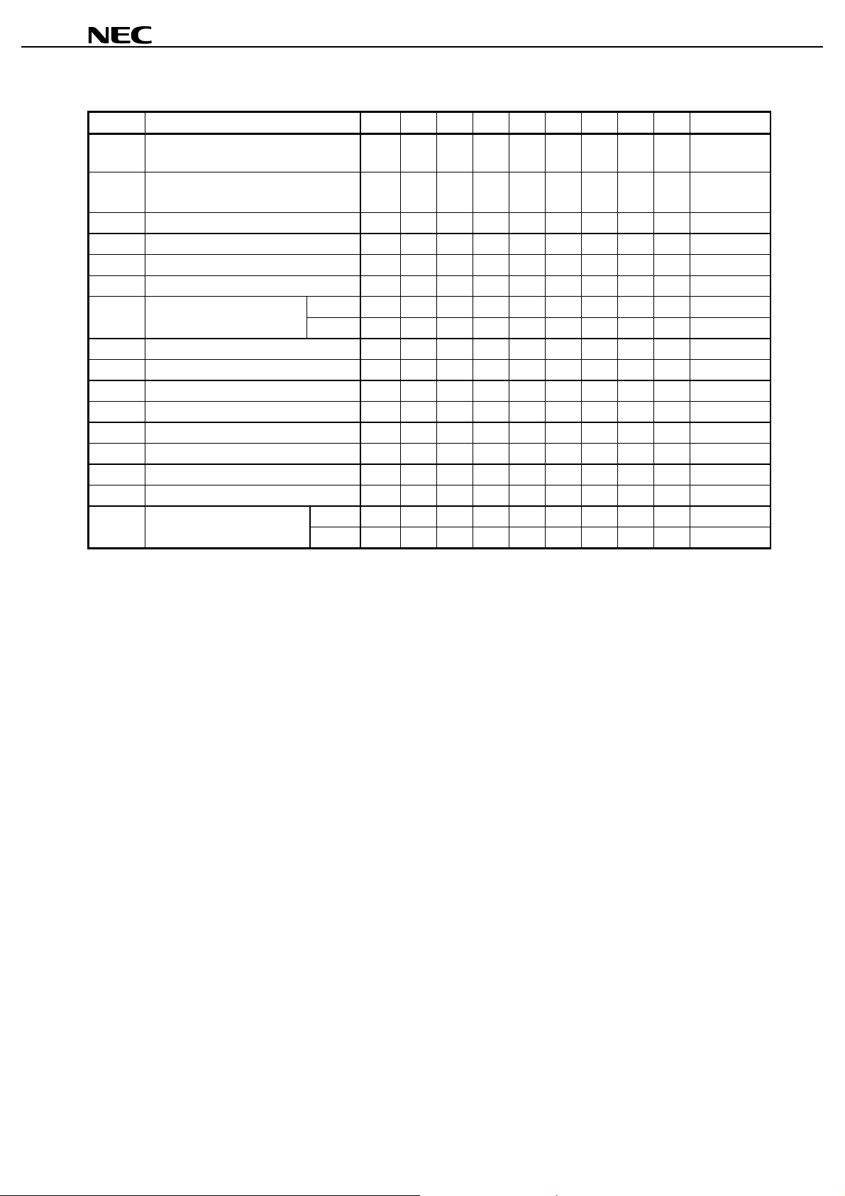
Ordering Information
MC-4532CD646
Part number Clock frequency
MHz (MAX.)
MC-4532CD646EF-A80 125 MHz 168-pin Dual In-line Memory Module 16 pieces of µPD45128841G5 (Rev. E)
MC-4532CD646EF-A10 100 MHz (Socket Type) (10.16 mm (400) TSOP (II))
MC-4532CD646PF-A80 125 MHz Edge connector : Gold pl ated 16 pieces of µPD45128841G5 (Rev. P)
★
MC-4532CD646PF-A10 100 MHz 34.93 mm hei ght (10.16 mm (400) TSOP (II))
★
Package Mounted devices
2
Data Sheet M13681EJ4V0DS00
Pin Configuration
★
168-pin Dual In-line Memory Module Socket Type (Edge connector: Gold plated)
MC-4532CD646
100
101
102
103
104
105
106
107
108
109
110
111
112
113
114
115
116
117
118
119
120
121
122
123
124
125
126
127
128
129
130
131
132
133
134
135
136
137
138
139
140
141
142
143
144
145
146
147
148
149
150
151
152
153
154
155
156
157
158
159
160
161
162
163
164
165
166
167
168
85
86
87
88
89
90
91
92
93
94
95
96
97
98
99
SS
V
DQ32
DQ33
DQ34
DQ35
Vcc
DQ36
DQ37
DQ38
DQ39
DQ40
SS
V
DQ41
DQ42
DQ43
DQ44
DQ45
Vcc
DQ46
DQ47
NC
NC
SS
V
NC
NC
Vcc
/CAS
DQMB4
DQMB5
/CS1
/RAS
SS
V
A1
A3
A5
A7
A9
(A13)
BA0
A11
Vcc
CLK1
NC
SS
V
CKE0
/CS3
DQMB6
DQMB7
NC
Vcc
NC
NC
NC
NC
SS
V
DQ48
DQ49
DQ50
DQ51
Vcc
DQ52
NC
NC
NC
SS
V
DQ53
DQ54
DQ55
SS
V
DQ56
DQ57
DQ58
DQ59
Vcc
DQ60
DQ61
DQ62
DQ63
SS
V
CLK3
NC
SA0
SA1
SA2
Vcc
V
DQ0
DQ1
DQ2
DQ3
Vcc
DQ4
DQ5
DQ6
DQ7
DQ8
V
DQ9
DQ10
DQ11
DQ12
DQ13
Vcc
DQ14
DQ15
NC
NC
V
NC
NC
Vcc
/WE
DQMB0
DQMB1
/CS0
NC
V
A10
BA1 (A12)
Vcc
Vcc
CLK0
V
NC
/CS2
DQMB2
DQMB3
NC
Vcc
NC
NC
NC
NC
V
DQ16
DQ17
DQ18
DQ19
Vcc
DQ20
NC
NC
CKE1
V
DQ21
DQ22
DQ23
V
DQ24
DQ25
DQ26
DQ27
Vcc
DQ28
DQ29
DQ30
DQ31
V
CLK2
NC
WP
SDA
SCL
Vcc
SS
SS
SS
SS
A0
A2
A4
A6
A8
SS
SS
SS
SS
SS
1
2
3
4
5
6
7
8
9
10
11
12
13
14
15
16
17
18
19
20
21
22
23
24
25
26
27
28
29
30
31
32
33
34
35
36
37
38
39
40
41
42
43
44
45
46
47
48
49
50
51
52
53
54
55
56
57
58
59
60
61
62
63
64
65
66
67
68
69
70
71
72
73
74
75
76
77
78
79
80
81
82
83
84
A0 - A11 : Address Inputs
[Row: A0 - A11, Column: A0 - A9]
BA0 (A13), BA1 (A12)
: SDRAM Bank Select
DQ0 - DQ63 : Data Inputs/Outputs
CLK0 - CLK3 : Clock Input
CKE0, CKE1 : Clock Enable Input
/CS0 - /CS3 : Chip Select Input
/RAS : Row Address Strobe
/CAS : Column Address Strobe
/WE : Write Enable
DQMB0 - DQMB7 : DQ Mask Enable
SA0 - SA2 :
Address Input for EEPROM
SDA : Serial Data I/O for PD
SCL : Clock Input for PD
CC
V
SS
V
: Power Supply
: Ground
WP : Write Protect
NC : No Connection
/xxx indica tes active low signal.
Data Sheet M13681EJ4V0DS00
3
Block Diagram
★
/WE
/CS0
DQMB0
DQ 0
DQ 1
DQ 2
DQ 3
DQ 4
DQ 5
DQ 6
DQ 7
DQMB1
DQ 8
DQ 9
DQ 10
DQ 11
DQ 12
DQ 13
DQ 14
DQ 15
DQMB4
DQ 32
DQ 33
DQ 34
DQ 35
DQ 36
DQ 37
DQ 38
DQ 39
DQMB5
DQ 40
DQ 41
DQ 42
DQ 43
DQ 44
DQ 45
DQ 46
DQ 47
DQ 7
DQ 6
DQ 5
DQ 4
DQ 3
DQ 2
DQ 1
DQ 0
DQ 7
DQ 6
DQ 5
DQ 4
DQ 3
DQ 2
DQ 1
DQ 0
DQ 4
DQ 7
DQ 6
DQ 5
DQ 3
DQ 2
DQ 1
DQ 0
DQ 5
DQ 7
DQ 6
DQ 4
DQ 3
DQ 2
DQ 1
DQ 0
DQM
DQM
DQM
DQM
MC-4532CD646
/CS1
DQ 0
DQ 1
DQ 2
DQ 3
DQ 4
DQ 5
DQ 6
DQ 7
DQ 0
DQ 1
DQ 2
DQ 3
DQ 4
DQ 5
DQ 6
DQ 7
DQ 3
DQ 0
DQ 1
DQ 2
DQ 4
DQ 5
DQ 6
DQ 7
DQ 2
DQ 0
DQ 1
DQ 3
DQ 4
DQ 5
DQ 6
DQ 7
DQM
DQM
DQM
DQM
/CS
D8
/CS
D9
/CS
D12
/CS
D13
/WE
/CS
D0
/WE
/CS
D1
/WE
/CS
D4
/CS
/WE
D5
/CS2 /CS3
DQMB2
/WE
/WE
/WE
/WE
DQ 16
DQ 17
DQ 18
DQ 19
DQ 20
DQ 21
DQ 22
DQ 23
DQMB3
DQ 24
DQ 25
DQ 26
DQ 27
DQ 28
DQ 29
DQ 30
DQ 31
DQMB6
DQ 48
DQ 49
DQ 50
DQ 51
DQ 52
DQ 53
DQ 54
DQ 55
DQMB7
DQ 56
DQ 57
DQ 58
DQ 59
DQ 60
DQ 61
DQ 62
DQ 63
DQM
DQ 7
DQ 6
DQ 5
DQ 4
DQ 3
DQ 2
DQ 1
DQ 0
DQM
DQ 4
DQ 7
DQ 6
DQ 5
DQ 3
DQ 2
DQ 1
DQ 0
DQM /CS /WE
DQ 7
DQ 6
DQ 5
DQ 4
DQ 3
DQ 2
DQ 1
DQ 0
DQM /CS /WE
DQ 7
DQ 6
DQ 5
DQ 4
DQ 3
DQ 2
DQ 1
DQ 0
/CS /WE
D2
/CS /WE
D3
D6
D7
DQ 0
DQ 1
DQ 2
DQ 3
DQ 4
DQ 5
DQ 6
DQ 7
DQ 3
DQ 0
DQ 1
DQ 2
DQ 4
DQ 5
DQ 6
DQ 7
DQ 0
DQ 1
DQ 2
DQ 3
DQ 4
DQ 5
DQ 6
DQ 7
DQ 0
DQ 1
DQ 2
DQ 3
DQ 4
DQ 5
DQ 6
DQ 7
DQM
DQM
DQM
DQM
D10
D11
D14
D15
/CS
/CS
/CS
/CS
/WE
/WE
/WE
/WE
SCL
A0 - A11
BA0, BA1
Remarks 1.
4
SERIAL PD
SDA
A1 A2
A0
SA1 SA2
SA0
A0 - A11: D0 - D15
A13, A12: D0 - D15
V
CC
V
SS
C
WP
47 kΩ
D0 - D15
D0 - D15
CLK0
3.3 pF
CLK1
3.3 pF
/RAS
/CAS
CKE0
The value of all resistors is 10 Ω except CKE1 and WP.
2.
D0 - D15:
µ
PD45128841 (4M words × 8 bits × 4 banks)
Data Sheet M13681EJ4V0DS00
CLK: D0, D1, D4, D5
CLK: D8, D9, D12, D13
/RAS: D0 - D15
/CAS: D0 - D15
CKE: D0 - D7
CLK2
CLK3
CKE1
CLK: D2, D3, D6, D7
3.3 pF
CLK: D10, D11, D14, D15
3.3 pF
10 kΩ
CKE: D8-D15
MC-4532CD646
Electrical Specifications
• All voltages are referenced to VSS (GND).
µ
• After power up, wait more than 100
device operation is achieved.
Absolute Maximum Ratings
Parameter Symbol Condition Rating Unit
Voltage on power supply pin relative to GND V
Voltage on input pin relative to GND V
Short circuit output c urrent I
Power dissipation P
Operating ambient tem perature T
Storage temperature T
Caution Exposing the device to stress above those listed in Absolute Maximum Ratings could cause
permanent damage. The device is not meant to be operated under conditions outside the limits
described in the operational section of this specification. Exposure to Absolute Maximum Rating
conditions for extended periods may affect device reliability.
s and then, execute power on sequence and CBR (Auto) refresh before proper
CC
T
O
D
A
stg
–0.5 to +4.6 V
–0.5 to +4.6 V
50 mA
16 W
0 to +70
–55 to +125
C
°
C
°
Recommended Operating Conditions
Parameter Symbol Condition MIN. TYP. MAX. Unit
Supply voltage V
High level input voltage V
Low level input voltage V
Operating ambient tem perature T
Capacitance (TA = 25
C, f = 1 MHz)
°°°°
Parameter Symbol Test condition MIN. TYP. MAX. Unit
Input capacitance CI1A0 - A11, BA0 (A13), BA1 (A12),
Data input/output capaci t ance C
CC
IH
IL
A
/RAS, /CAS, /WE
CI2CLK0 - CLK3 24 40
CI3CKE0, CKE1 32 52
CI4/CS0 - /CS3 17 29
CI5DQMB0 - DQMB7 10 17
I/O
DQ0 - DQ63 11 19 pF
3.0 3.3 3.6 V
2.0 V
0.3 +0.8 V
−
070
CC
0.3 V
+
C
°
58 94 pF
Data Sheet M13681EJ4V0DS00
5
DC Characteristics (Recommended Operating Conditions Unless Otherwise Noted)
Parameter Symbol Test condition Grade MIN. MAX. Unit Notes
•
•
Operating current I
CC1
Burst length = 1
RC ≥ tRC(MIN.)
t
/CAS latency = 2
, IO = 0 mA -A10 1,040
/CAS latency = 3
•
•
•
•
•
Precharge standby current in I
power down mode I
Precharge standby current in
non power down mode
CC2
P CKE ≤ V
CC2
PS CKE ≤ V
CC2
I
NCKE
Input signals are changed one time during 30
CC2
I
NS CKE ≥ V
Input signals are stable.
Active standby current i n I
power down mode I
Active standby current i n I
CC3
P CKE ≤ V
CC3
PS CKE ≤ V
CC3
NCKE
non power down mode Input si gnal s are changed one time during 30 ns.
CC3
I
NS CKE ≥ V
Operating current I
CC4tCK ≥ tCK(MIN.)
(Burst mode) IO = 0 mA -A10 1,000
IL(MAX.)
IL(MAX.)
≥ VIH(MIN.)
IH(MIN.)
IL(MAX.)
IL(MAX.)
≥ VIH(MIN.)
IH(MIN.)
CK = 15
, t
, t
, t
, t
, t
, t
, t
, t
ns 16 mA
CK =
∞
CK = 15
CK =
∞
CK = 15
CK =
∞
CK = 15
CK =
∞
≥ VIH(MIN.)
ns, /CS
,
ns 80 mA
≥ VIH(MIN.)
ns, /CS
, 400 mA
, Input signals are st abl e. 320
/CAS latency = 2
/CAS latency = 3
•
•
CBR (Auto) refresh current I
CC5tRC ≥ tRC(MIN.)
/CAS latency = 2
•
•
/CAS latency = 3
•
Self refresh current I
Input leakage current I
Input leakage current (CKE1) – 500 +500
Output leakage current I
High level output voltage VOHIO = – 4.0 mA 2.4 V
Low level output voltage VOLIO = + 4.0 mA 0.4 V
CC6
CKE ≤ 0.2 V32mA
=
I(L)VI
O(L)DOUT
0 to 3.6 V, All other pins not under test = 0 V – 16 + 16µA
is disabled, VO = 0 to 3.6 V–
ns.
MC-4532CD646
-A80 1,040 mA 1
-A80 1,040
-A10 1,040
16
320 mA
96
64
-A80 1,200 mA 2
-A80 1,400
-A10 1,240
-A80 2,080 mA 3
-A10 2,080
-A80 2,080
-A10 2,080
3+ 3µA
Notes 1.
6
CC1
I
depends on output loading and cycle rates. Specified values are obtained with the output open. In
CC1
addition to this, I
CC4
2
.I
depends on output loading and cycle rates. Specified values are obtained with the output open. In
addition to this, I
CC5
3.
I
is measured on condition that addresses are changed only one time during t
is measured on condition that addresses are changed only one time during t
CC4
is measured on condition that addresses are changed only one time during t
CK (MIN.)
.
Data Sheet M13681EJ4V0DS00
CK (MIN.)
CK (MIN.)
.
.
AC Characteristics (Recommended Operating Conditions Unless Otherwise Noted)
Test Conditions
★
Parameter Value Unit
AC high level input voltage / low level input voltage 2.4 / 0.4 V
Input timing measurement ref erence level 1.4 V
Transition time (Input rise and fall time) 1 ns
Output timing measurement ref erence level 1.4 V
t
CK
t
CH
2.4 V
CLK
Input
1.4 V
0.4 V
2.4 V
1.4 V
0.4 V
t
SETUPtHOLD
t
AC
t
OH
MC-4532CD646
Notes
t
CL
Output
Data Sheet M13681EJ4V0DS00
7
Synchronous Characteristics
Parameter Symbol -A80 -A10 Unit Note
Clock cycle time /CAS latency = 3 t
/CAS latency = 2 t
Access time from CLK /CAS latency = 3 t
/CAS latency = 2 t
CLK high level width t
CLK low level width t
Data-out hold time t
Data-out low-impedance tim e t
Data-out high-impedance time / CA S l atency = 3 t
/CAS latency = 2 t
Data-in setup time t
Data-in hold time t
Address setup time t
Address hold time t
CKE setup time t
CKE hold time t
CKE setup time (P ower down exit) t
Command (/CS0 - /CS 3, /RAS, /CAS, / WE,
DQMB0 - DQMB7) setup time
Command (/CS0 - /CS 3, /RAS, /CAS, / WE,
DQMB0 - DQMB7) hold time
CK3
CK2
AC3
AC2
CH
OH
HZ3
HZ2
DS
DH
AH
CKS
CKH
CKSP
CMS
t
CMH
t
MC-4532CD646
MIN. MAX. MIN. MAX.
8 (125 MHz) 10 (100 MHz) ns
10 (100 MHz) 13 (77 MHz) ns
66ns1
67ns1
33ns
CL
LZ
AS
33ns
33ns1
00ns
3636ns
3637ns
22ns
11ns
22ns
11ns
22ns
11ns
22ns
22ns
11ns
★
Note 1.
Output load
Z = 50 Ω
Output
50 pF
Remark
These specifications are applied to the monolithic device.
8
Data Sheet M13681EJ4V0DS00

Asynchronous Characteristics
Parameter Symbol -A80 -A10 Unit Note
ACT to REF/ACT comm and peri od (Operat i on) t
REF to REF/ACT command period (Refresh) t
ACT to PRE command period t
PRE to ACT command period t
Delay time ACT to READ/WRITE command t
ACT(one) to ACT(another) command period t
Data-in to PRE command period t
Data-in to ACT(REF) command period /CAS latency = 3 t
(Auto precharge) /CAS latency = 2 t
Mode register set cycle time t
Transition time t
Refresh time (4,096 refres h cycles) t
MIN. MAX. MIN. MAX.
RC
RC1
RAS
RP
RCD
RRD
DPL
DAL3
DAL2
RSC
T
REF
70 70 ns
70 78 ns
48 120,000 50 120,000 ns
20 20 ns
20 20 ns
16 20 ns
810ns
1CLK+20 1CLK+20 ns
1CLK+20 1CLK+20 ns
22CLK
0.5 30 1 30 ns
64 64 ms
MC-4532CD646
Data Sheet M13681EJ4V0DS00
9
MC-4532CD646
Serial PD
Byte No. Function Described Hex Bit 7 Bit 6 Bit 5 Bit 4 Bit 3 Bit 2 Bit 1 Bit 0 Notes
0 Defines the num ber of bytes written into
serial PD memory
1 Total number of bytes of serial PD memory 08H 0 0 0 0 1 0 0 0 256 bytes
2 Fundament al memory type 04H 0 0 0 0 0 1 0 0 SDRAM
3 Number of rows 0CH 0 0 0 0 1 1 0 0 12 rows
4 Number of c ol umns 0AH 0 0 0 0 1 0 1 0 10 columns
5 Number of bank s 02H 0 0 0 0 0 0 1 0 2 banks
6 Data width 40H 0 1 0 0 0 0 0 0 64 bits
7 Data width (continued) 00H 0 0 0 0 0 0 0 0 0
8 Voltage interf ace 01H 0 0 0 0 0 0 0 1 LVTTL
9 CL = 3 Cycle time -A80 80H 1 0 0 0 0 0 0 0 8 ns
-A10 A0H 1 0 1 0 0 0 0 0 10 ns
10 CL = 3 Access ti me -A80 60H 0 1 1 0 0 0 0 0 6 ns
-A10 60H 0 1 1 0 0 0 0 0 6 ns
11 DIMM configuration type 00H 0 0 0 0 0 0 0 0 None
12 Refresh rate/type 80H 1 0 0 0 0 0 0 0 Normal
13SDRAM width 08H00001000×8
14 Error checking SDRA M width 00H 0 0 0 0 0 0 0 0 None
15 Minimum clock delay 01H 0 0 0 0 0 0 0 1 1 clock
16 Burst length supported 8FH 1 0 0 0 1 1 1 1 1, 2, 4, 8, F
17 Number of banks on each S DRAM 04H 0 0 0 0 0 1 0 0 4 banks
18 /CAS latency support ed 06H 0 0 0 0 0 1 1 0 2, 3
19 /CS latency supported 01H 0 0 0 0 0 0 0 1 0
20 /WE l at ency supported 01H 0 0 0 0 0 0 0 1 0
21 SDRAM module attribut es 00H 0 0 0 0 0 0 0 0
22 SDRAM device attributes : General 0EH 0 0 0 0 1 1 1 0
23 CL = 2 Cycle time -A80 A0H 1 0 1 0 0 0 0 0 10 ns
-A10 D0H 1 1 0 1 0 0 0 0 13 ns
24 CL = 2 Access ti me -A80 60H 0 1 1 0 0 0 0 0 6 ns
-A10 70H 0 1 1 1 0 0 0 0 7 ns
25-26 00H 0 0 0 0 0 0 0 0
RP(MIN.)
27 t
-A80 14H 0 0 0 1 0 1 0 0 20 ns
-A10 14H 0 0 0 1 0 1 0 0 20 ns
RRD(MIN.)
28 t
-A80 10H 0 0 0 1 0 0 0 0 16 ns
-A10 14H 0 0 0 1 0 1 0 0 20 ns
RCD(MIN.)
29 t
-A80 14H 0 0 0 1 0 1 0 0 20 ns
-A10 14H 0 0 0 1 0 1 0 0 20 ns
RAS(MIN.)
30 t
-A80 30H 0 0 1 1 0 0 0 0 48 ns
-A10 32H 0 0 1 1 0 0 1 0 50 ns
31 Module bank density 20H 0 0 1 0 0 0 0 0 128M bytes
80H 1 0 0 0 0 0 0 0 128 bytes
(1/2)
10
Data Sheet M13681EJ4V0DS00
MC-4532CD646
(2/2)
Byte No. Function Described Hex Bit 7 Bit 6 Bit 5 Bit 4 Bit 3 Bit 2 Bit 1 Bit 0 Notes
32 Command and address signal i nput
setup time
33 Command and address signal i nput
hold time
34 Data signal input setup ti me 20H 0 0 1 0 0 0 0 0 2 ns
35 Data signal input hold time 10H 0 0 0 1 0 0 0 0 1 ns
36-61 00H 0 0 0 0 0 0 0 0
62 SPD revision 12H 0 0 0 1 0 0 1 0 1.2
63 Checksum for bytes 0 - 62 -A80 F1H 1 1 1 1 0 0 0 1
-A1057H01010111
64-71 Manufacture’s JEDEC ID code
72 Manufacturing location
73-90 Manufacture’s P/N
91-92 Revision code
93-94 Manufacturing date
95-98 Assembly serial number
99-125 Mfg specifi c
126 Intel specification frequency 64H 0 1 1 0 0 1 0 0 100 MHz
127 Intel specificati on / CA S -A80 FFH 1 1 1 1 1 1 1 1
latency support -A10 FDH 1 1 1 1 1 1 0 1
20H001000002 ns
10H000100001 ns
Timing Chart
Refer to the
SYNCHORONOUS DRAM MODULE TIMING CHART Information (M13348E)
.
Data Sheet M13681EJ4V0DS00
11

★
Package Drawing
168 PIN DUAL IN-LINE MODULE (SOCKET TYPE)
A (AREA B)
Y1
R2
F1
Y2
Z1
Z2
MC-4532CD646
N
F2
Q
M
R1
M2 (AREA A)
M1 (AREA B)
L
A
J
H
K
CB
GI
B
S
(OPTIONAL HOLES)
E
U1
U2
T
D
A1 (AREA A)
ITEM MILLIMETERS
A
133.35
133.35±0.13
A1
11.43
B
C 36.83
D 6.35
D1 2.0
3.125
D2
E 54.61
2.44
F1
F2 3.18
detail of A part
W
V
X
detail of B part
D2
P
D1
G 6.35
H 1.27 (T.P.)
I 8.89
24.495
J
K 42.18
17.78
L
34.93±0.13
M
15.15
M1
M2 19.78
N 4.0 MAX.
1.0
P
Q R2.0
R1 4.0±0.10
R2 9.53
φ
S
T
U1 4.0 MIN.
U2
V 0.2±0.15
W 1.0±0.05
X
Y1 3.0 MIN.
Y2 2.26
Z1
Z2 2.26
3.0
1.27±0.1
4.0 MIN.
2.54±0.10
3.0 MIN.
M168S-50A78
12
Data Sheet M13681EJ4V0DS00

[MEMO]
MC-4532CD646
Data Sheet M13681EJ4V0DS00
13

[MEMO]
MC-4532CD646
14
Data Sheet M13681EJ4V0DS00
MC-4532CD646
NOTES FOR CMOS DEVICES
1 PRECAUTION AGAINST ESD FOR SEMICONDUCTORS
Note:
Strong electric field, when exposed to a MOS device, can cause destruction of the gate oxide and
ultimately degrade the device operation. Steps must be taken to stop generation of static electricity
as much as possible, and quickly dissipate it once, when it has occurred. Environmental control
must be adequate. When it is dry, humidifier should be used. It is recommended to avoid using
insulators that easily build static electricity. Semiconductor devices must be stored and transported
in an anti-static container, static shielding bag or conductive material. All test and measurement
tools including work bench and floor should be grounded. The operator should be grounded using
wrist strap. Semiconductor devices must not be touched with bare hands. Similar precautions need
to be taken for PW boards with semiconductor devices on it.
2 HANDLING OF UNUSED INPUT PINS FOR CMOS
Note:
No connection for CMOS device inputs can be cause of malfunction. If no connection is provided
to the input pins, it is possible that an internal input level may be generated due to noise, etc., hence
causing malfunction. CMOS devices behave differently than Bipolar or NMOS devices. Input levels
of CMOS devices must be fixed high or low by using a pull-up or pull-down circuitry. Each unused
DD
pin should be connected to V
being an output pin. All handling related to the unused pins must be judged device by device and
related specifications governing the devices.
or GND with a resistor, if it is considered to have a possibility of
3 STATUS BEFORE INITIALIZATION OF MOS DEVICES
Note:
Power-on does not necessarily define initial status of MOS device. Production process of MOS
does not define the initial operation status of the device. Immediately after the power source is
turned ON, the devices with reset function have not yet been initialized. Hence, power-on does
not guarantee out-pin levels, I/O settings or contents of registers. Device is not initialized until the
reset signal is received. Reset operation must be executed immediately after power-on for devices
having reset function.
Data Sheet M13681EJ4V0DS00
15
MC-4532CD646
CAUTION FOR HANDLING MEMORY MODULES
When handling or inserting memory modules, be sure not to touch any components on the modules, such as
the memory IC, chip capacitors and chip resistors. It is necessary to avoid undue mechanical stress on these
components to prevent damaging them.
When re-packing memory modules, be sure the modules are NOT touching each other. Modules in contact
with other modules may cause excessive mechanical stress, which may damage the modules.
• The information in this document is subject to change without notice. Before using this document, please
confirm that this is the latest version.
• No part of this document may be copied or reproduced in any form or by any means without the prior written
consent of NEC Corporation. NEC Corporation assumes no responsibility for any errors which may appear in
this document.
• NEC Corporation does not assume any liability for infringement of patents, copyrights or other intellectual property
rights of third parties by or arising from use of a device described herein or any other liability arising from use
of such device. No license, either express, implied or otherwise, is granted under any patents, copyrights or other
intellectual property rights of NEC Corporation or others.
• Descriptions of circuits, software, and other related information in this document are provided for illustrative
purposes in semiconductor product operation and application examples. The incorporation of these circuits,
software, and information in the design of the customer's equipment shall be done under the full responsibility
of the customer. NEC Corporation assumes no responsibility for any losses incurred by the customer or third
parties arising from the use of these circuits, software, and information.
• While NEC Corporation has been making continuous effort to enhance the reliability of its semiconductor devices,
the possibility of defects cannot be eliminated entirely. To minimize risks of damage or injury to persons or
property arising from a defect in an NEC semiconductor device, customers must incorporate sufficient safety
measures in its design, such as redundancy, fire-containment, and anti-failure features.
• NEC devices are classified into the following three quality grades:
"Standard", "Special", and "Specific". The Specific quality grade applies only to devices developed based on a
customer designated "quality assurance program" for a specific application. The recommended applications of
a device depend on its quality grade, as indicated below. Customers must check the quality grade of each device
before using it in a particular application.
Standard: Computers, office equipment, communications equipment, test and measurement equipment,
audio and visual equipment, home electronic appliances, machine tools, personal electronic
equipment and industrial robots
Special: Transportation equipment (automobiles, trains, ships, etc.), traffic control systems, anti-disaster
systems, anti-crime systems, safety equipment and medical equipment (not specifically designed
for life support)
Specific: Aircraft, aerospace equipment, submersible repeaters, nuclear reactor control systems, life
support systems or medical equipment for life support, etc.
The quality grade of NEC devices is "Standard" unless otherwise specified in NEC's Data Sheets or Data Books.
If customers intend to use NEC devices for applications other than those specified for Standard quality grade,
they should contact an NEC sales representative in advance.
M7 98. 8
 Loading...