NEC UPD70F3003AGC-33-8EU, UPD70F3003AGC-25-8EU Datasheet
DATA SHEET
MOS INTEGRATED CIRCUIT
µ
PD70F3003A, 70F3025A
V853
TM
32-/16-BIT SINGLE-CHIP MICROCONTROLLER
DESCRIPTION
The µPD70F3003A and µPD70F3025A have a flash memory instead of the internal mask ROM of the µPD703003A/
703004A and µPD703025A, respectively. This model is useful for small-scale production of a variety of application
sets or early start of production since the program can be written and erased by the user even with the µPD70F3003
mounted on the board.
Functions in detail are described in the following user’s manuals. Be sure to read these manuals when
you design your systems.
V853 User’s Manual-Hardware : U10913E
TM
V850 Family
FEATURES
• Compatible with µPD703003A, 703004A and 703025A
• Can be replaced with mask ROM model for mass production of application set
µ
PD70F3003A → µPD703003A, 703004A
µPD70F3025A → µPD703025A
• Internal memory Flash memory: 128K bytes (
User’s Manual-Architecture : U10243E
µ
PD70F3003A)
256K bytes (µPD70F3025A)
Remark For differences among the products, refer to 1. DIFFERENCES AMONG PRODUCT.
ORDERING INFORMATION
Part Number Package Maximum Operating Frequency (MHz)
µ
PD70F3003AGC-25-8EU
µ
PD70F3003AGC-33-8EU
µ
PD70F3025AGC-25-8EU
µ
PD70F3025AGC-33-8EU
Note Under development
The information in this document is subject to change without notice. Before using this document, please
confirm that this is the latest version.
Not all devices/types available in every country. Please check with local NEC representative for availability
and additional information.
Document No. U13189EJ3V0DS00 (3rd edition)
Date Published May 2000 N CP(K)
Printed in Japan
Note
Note
100-pin plastic LQFP (fine pitch) (14 × 14 mm)
100-pin plastic LQFP (fine pitch) (14 × 14 mm)
100-pin plastic LQFP (fine pitch) (14 × 14 mm)
100-pin plastic LQFP (fine pitch) (14 × 14 mm)
The mark shows major revised points.
25
33
25
33
©
1998
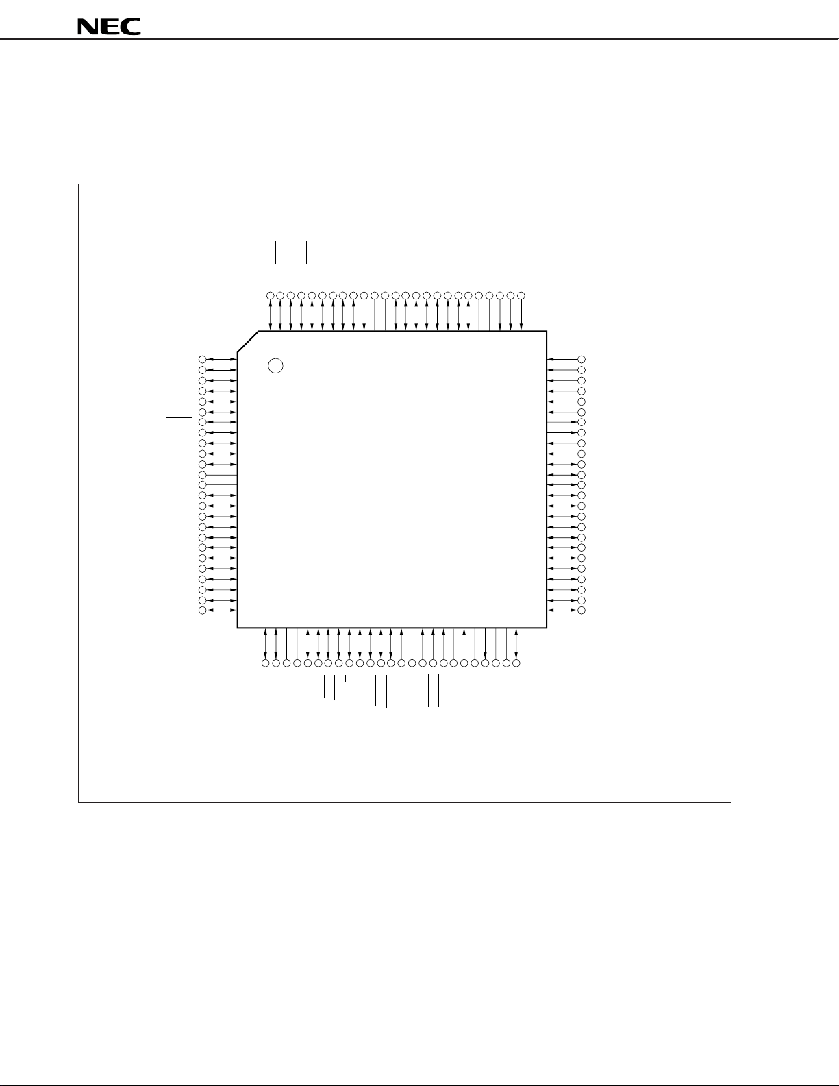
PIN CONFIGURATION (Top View)
• 100-Pin Plastic LQFP (fine pitch) (14 × 14 mm)
µ
PD70F3003AGC-25-8EUµPD70F3025AGC-25-8EU
µ
PD70F3003AGC-33-8EUµPD70F3025AGC-33-8EU
P30/TO130
P27/SCK1
P26/RXD1/SI1
P25/TXD1/SO1
P24/SCK0
P23/RXD0/SI0
P22/TXD0/SO0
P21/PWM1
P20/PWM0
NMI
VDDVSSP17/INTP123/SCK2
P16/INTP122/SI2
P15/INTP121/SO2
P14/INTP120
P13/TI12
P12/TCLR12
P11/TO121
P10/TO120
AVDDAVSSAVREF1
µ
PD70F3003A, 70F3025A
P77/ANI7
P76/ANI6
P31/TO131
P32/TCLR13
P33/TI13
P34/INTP130
P35/INTP131/SO3
P36/INTP132/SI3
P37/INTP133/SCK3
P63/A19
P62/A18
P61/A17
P60/A16
V
V
P57/AD15
P56/AD14
P55/AD13
P54/AD12
P53/AD11
P52/AD10
P51/AD9
P50/AD8
P47/AD7
P46/AD6
P45/AD5
P44/AD4
9998979695949392919089888786858483828180797877
100
1
2
3
4
5
6
7
8
9
10
11
SS
DD
12
13
14
15
16
17
18
19
20
21
22
23
24
25
26272829303132333435363738394041424344454647484950
SS
V
P43/AD3
P42/AD2
DD
V
P41/AD1
P40/AD0
P90/LBEN
P91/UBEN
P92/R/W
P94/ASTB
P93/DSTB
PP
V
WAIT
MODE
P95/HLDAK
P96/HLDRO
X2
RESET
DD/CKSEL
CV
X1
SS
CV
SS
DD
V
V
CLKOUT
76
75
74
73
72
71
70
69
68
67
66
65
64
63
62
61
60
59
58
57
56
55
54
53
52
51
P110/TO140
P75/ANI5
P74/ANI4
P73/ANI3
P72/ANI2
P71/ANI1
P70/ANI0
ANO0
ANO1
AV
REF2
AV
REF3
P07/INTP113/ADTRG
P06/INTP112
P05/INTP111
P04/INTP110
P03/TI11
P02/TCLR11
P01/TO111
P00/TO110
P117/INTP143
P116/INTP142
P115/INTP141
P114/INTP140
P113/TI14
P112/TCLR14
P111/TO141
Caution Connect VPP pin to VSS pin except the case that µPD70F3003A or 70F3025A is used in flash
memory programming mode.
2
Data Sheet U13189EJ3V0DS00

PIN NAMES
µ
PD70F3003A, 70F3025A
A16-A19 : Address Bus
AD0-AD15 : Address/Data Bus
ADTRG : AD Trigger Input
ANI0-ANI7 : Analog Input
ANO0, ANO1 : Analog Output
ASTB : Address Strobe
DD : Analog VDD
AV
AVREF1-AVREF3 : Analog Reference Voltage
AVSS : Analog V SS
CVDD :
CVSS : Ground for Clock Generator
CKSEL : Clock Select
CLKOUT : Clock Output
DSTB : Data Strobe
HLDAK : Hold Acknowledge
HLDRQ : Hold Request
INTP110-INTP113, :
INTP120-INTP123,
INTP130-INTP133,
INTP140-INTP143
LBEN : Lower Byte Enable
MODE : Mode
NMI :
P00-P07 : Port0
P10-P17 : Port1
P20-P27 : Port2
P30-P37 : Port3
Power Supply for Clock Generator
Interrupt Request from Peripherals
Non-maskable Interrupt Request
P40-P47 : Port4
P50-P57 : Port5
P60-P63 : Port6
P70-P77 : Port7
P90-P96 : Port9
P110-P117 : Port11
PWM0, PWM1 : Pulse Width Modulation
RESET : Reset
R/W : Read/Write Status
RXD0, PXD1 : Receive Data
SCK0-SCK3 : Serial Clock
SI0-SI3 : Serial Input
SO0-SO3 : Serial Output
TO110, TO111, : Timer Output
TO120, TO121,
TO130, TO131,
TO140, TO141
TCLR11-TCLR14 : Timer Clear
TI11-TI14 : Timer Input
TXD0, TXD1 : Transmit Data
UBEN : Upper Byte Enable
WAIT : Wait
X1, X2 : Crystal
DD : Power Supply
V
VPP :
VSS : Ground
Programming Power Supply
Data Sheet U13189EJ3V0DS00
3
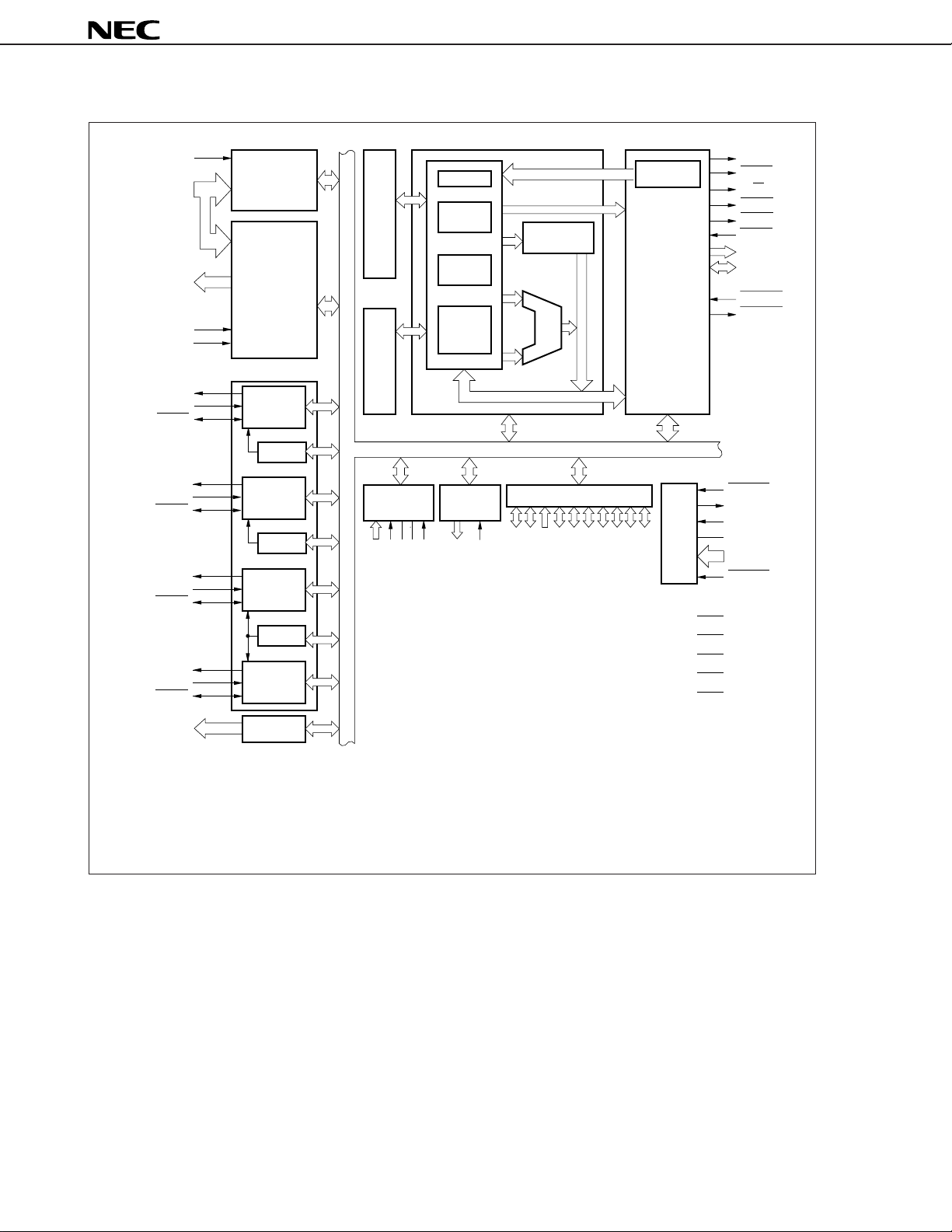
INTERNAL BLOCK DIAGRAM
µ
PD70F3003A, 70F3025A
NMI
INTP110-INTP113
INTP120-INTP123
INTP130-INTP133
INTP140-INTP143
TO110, TO111
TO120, TO121
TO130, TO131
TO140, TO141
TCLR11-TCLR14
TI11-TI14
SO0/TXD0
SI0/RXD0
SCK0
SO1/TXD1
SI1/RXD1
SCK1
SO2
SI2
SCK2
SO3
SI3
SCK3
INTC
RPU
SIO
UART0/CSI0
BRG0
UART1/CSI1
BRG1
CSI2
BRG2
CSI3
Flash memory
Note 1
RAM
Note 2
A/D
Converter
SS
REF1
AV
AV
ANI0-ANI7
32-bit
barrel shifter
System
register
Generalpurpose
register
32 bits × 32
D/A
Converter
DD
AV
ADTRG
CPU
PC
REF3
, AV
REF2
ANO0, ANO1
AV
Multiplier
16 × 16 → 32
ALU
Ports
P90-P96
P70-P77
P60-P63
P110-P117
P50-P57
P40-P47
P30-P37
Instruction
queue
BCU
P20-P27
P10-P17
P00-P07
CG
ASTB
DSTB
R/W
UBEN
LBEN
WAIT
A16-A19
AD0-AD15
HLDRQ
HLDAK
CKSEL
CLKOUT
X1
X2
MODE
RESET
V
DD
V
SS
CV
DD
CV
SS
V
PP
PWM0, PWM1
PWM
Notes1. µPD70F3003A: 128K bytes
µ
PD70F3025A: 256K bytes
2.µPD70F3003A: 4K bytes
µ
PD70F3025A: 8K bytes
4
Data Sheet U13189EJ3V0DS00

µ
PD70F3003A, 70F3025A
CONTENTS
1. DIFFERENCES AMONG PRODUCTS ······························································································ 6
2. PIN FUNCTIONS································································································································ 7
2.1 Port Pins····················································································································································· 7
2.2 Pins Other Than Port Pins ························································································································ 9
2.3 I/O Circuits of Pins and Recommended Connections of Unused Pins ················································ 11
3. ELECTRICAL SPECIFICATIONS ······································································································· 14
3.1 Normal Operation Mode···························································································································· 14
3.2 Flash Memory Programming Mode·········································································································· 35
4. PACKAGE DRAWING ······················································································································· 37
5. RECOMMENDED SOLDERING CONDITIONS················································································· 38
Data Sheet U13189EJ3V0DS00
5
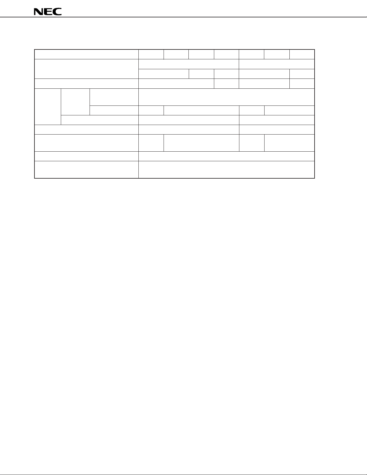
1. DIFFERENCES AMONG PRODUCTS
µ
PD70F3003A, 70F3025A
Parameter
Internal ROM Mask ROM Flash memory
Internal RAM 4K bytes
Operation Normal Single chip Provided
mode operation mode
mode
Flash memory programming mode
VPP pin None Provided
CKC register value at reset 00H MODE = 0: 03H 00H
Electrical specifications Current consumption, etc. differs. (Refer to each product data sheets.)
Others Noise immunity and noise radiation differ because circuit scale and mask
ROM-less mode
µ
PD703003µPD703003AµPD703004AµPD703025AµPD70F3003µPD70F3003AµPD70F3025A
128K bytes 96K bytes
Provided None Provided None
None Provided
MODE = 1: 00H
layout differ.
256K bytes
8K bytes
128K bytes
4K bytes
256K bytes
8K bytes
MODE = 0: 03H
MODE = 1: 00H
6
Data Sheet U13189EJ3V0DS00
µ
PD70F3003A, 70F3025A
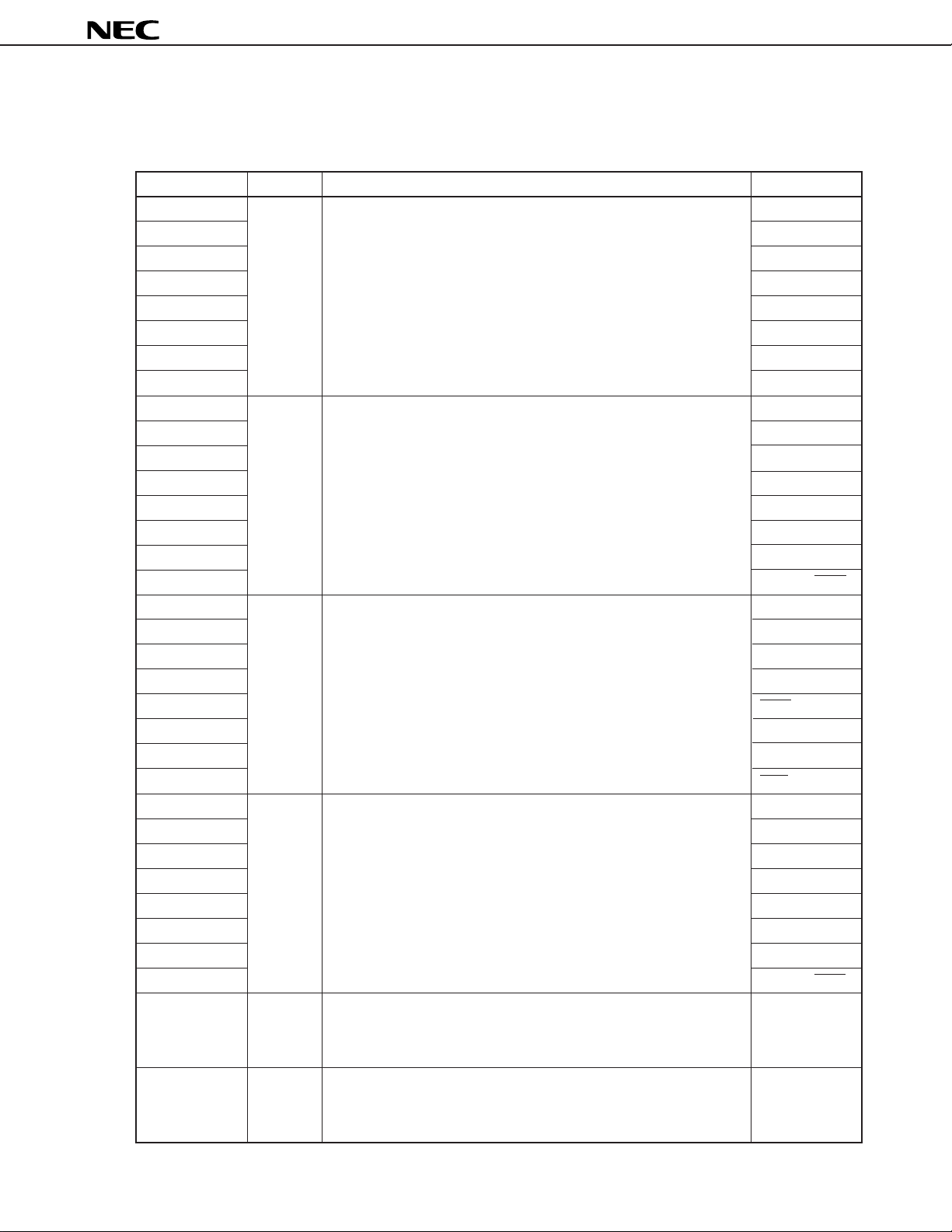
2. PIN FUNCTIONS
2.1 Port Pins
Pin Name I/O Function Shared with:
P00 I/O Port 0 TO110
P01 8-bit I/O port. TO111
P02 Can be set in input or output mode in 1-bit units. TCLR11
P03 TI11
P04 INTP110
P05 INTP111
P06 INTP112
P07
P10 I/O Port 1 TO120
P11 8-bit I/O port. TO121
P12 Can be set in input or output mode in 1-bit units. TCLR12
P13 TI12
P14 INTP120
P15 INTP121/SO2
P16 INTP122/SI2
P17
P20 I/O Port 2 PWM0
P21 8-bit I/O port. PWM1
P22 Can be set in input or output mode in 1-bit units. TXD0/SO0
P23 RXD0/SI0
P24 SCK0
P25 TXD1/SO1
P26 RXD1/SI1
P27
P30 I/O Port 3 TO130
P31 8-bit I/O port. TO131
P32 Can be set in input or output mode in 1-bit units. TCLR13
P33 TI13
P34 INTP130
P35 INTP131/SO3
P36 INTP132/SI3
P37
P40-P47 I/O Port 4 AD0-AD7
8-bit I/O port.
Can be set in input or output mode in 1-bit units.
P50-P57 I/O Port 5 AD8-AD15
8-bit I/O port.
Can be set in input or output mode in 1-bit units.
INTP113/ADTRG
I
NTP123/SCK2
SCK1
I
NTP133/SCK3
(1/2)
Data Sheet U13189EJ3V0DS00
7

µ
PD70F3003A, 70F3025A
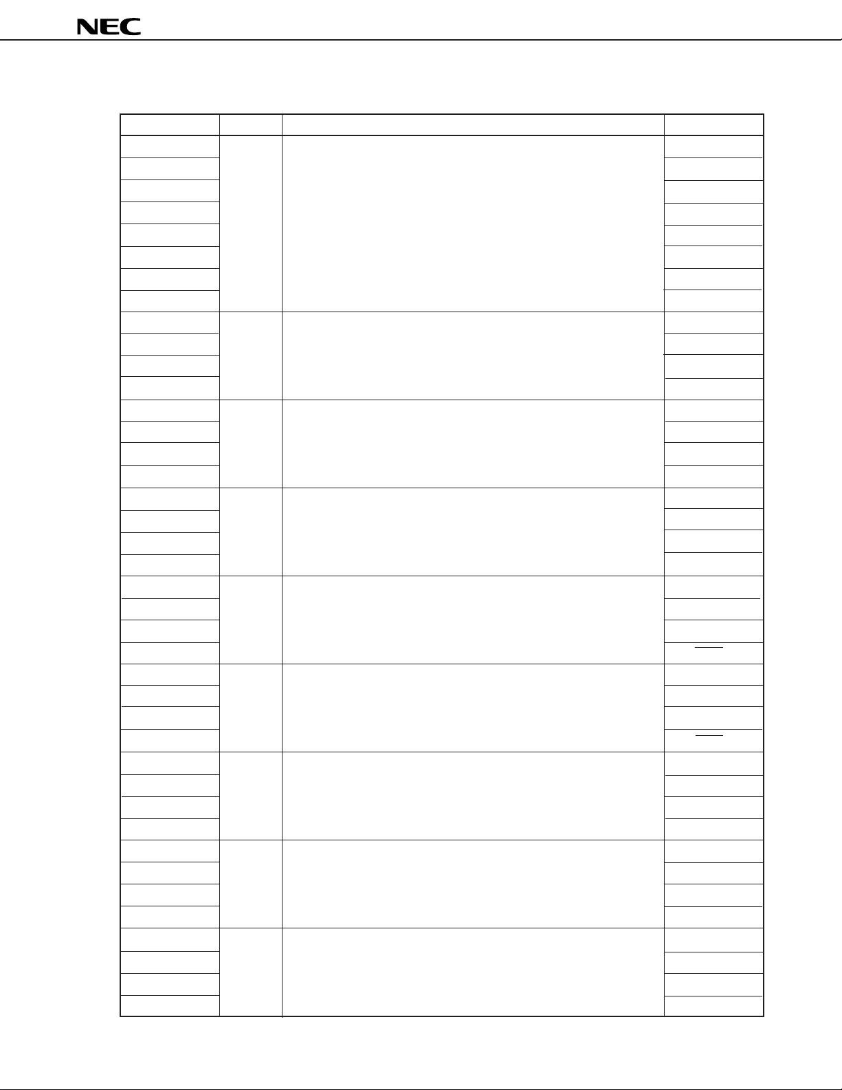
Pin Name I/O Function Shared with:
P60-P63 I/O Port 6 A16-A19
4-bit I/O port.
Can be set in input or output mode in 1-bit units.
P70-P77 Input Port 7 ANI0-ANI7
8-bit input port.
P90 I/O Port 9 LBEN
P91 7-bit I/O port. UBEN
P92 Can be set in input or output mode in 1-bit units. R/W
P93 DSTB
P94 ASTB
P95 HLDAK
P96 HLDRQ
P110 I/O Port 11 TO140
P111 8-bit I/O port. TO141
P112 Can be set in input or output mode in 1-bit units. TCLR14
P113 TI14
P114 INTP140
P115 INTP141
P116 INTP142
P117 INTP143
(2/2)
8
Data Sheet U13189EJ3V0DS00
µ
PD70F3003A, 70F3025A
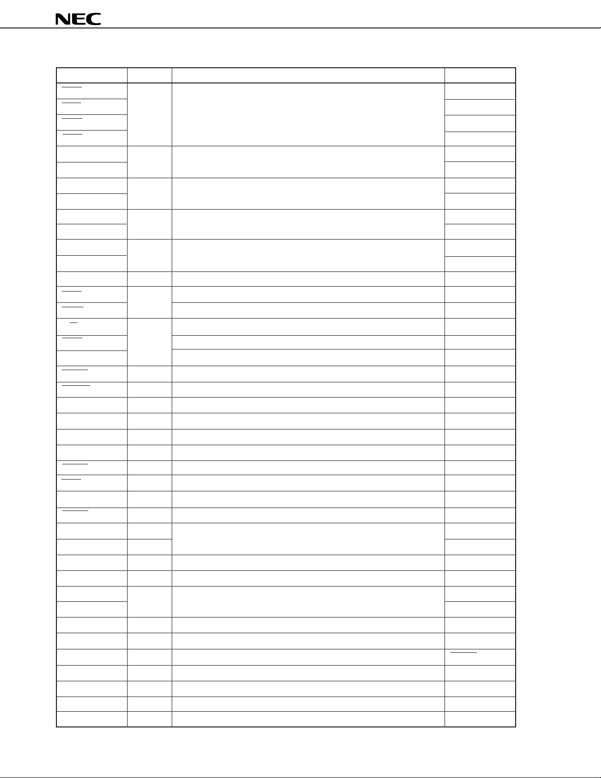
2.2 Pins Other Than Port Pins
Pin Name I/O Function Shared with:
TO110 Output Pulse signal output of timer 11-14 P00
TO111 P01
TO120 P10
TO121 P11
TO130 P30
TO131 P31
TO140 P110
TO141 P111
TCLR11 Input External clear signal of timer 11-14 P02
TCLR12 P12
TCLR13 P32
TCLR14 P112
TI11 Input External count clock of timer 11-14 P03
TI12 P13
TI13 P33
TI14 P113
INTP110 Input External maskable interrupt reuest input and external capture P04
INTP111
INTP112 P06
INTP113 P07/ADTRG
INTP120 Input External maskable interrupt reuest input and external capture P14
INTP121
INTP122 P16/S12
INTP123 P17/SCK2
INTP130 Input External maskable interrupt reuest input and external capture P34
INTP131
INTP132 P36/SI3
INTP133 P37/SCK3
INTP140 Input External maskable interrupt reuest input and external capture P114
INTP141
INTP142 P116
INTP143 P117
SO0 Output Serial transmit data output of CSI0-CSI3 (3 wire) P22/TXD0
SO1 P25/TXD1
SO2 P15/INTP121
SO3 P35/INTP131
SI0 Input Serial receive data output of CSI0-CSI3 (3 wire) P23/RXD0
SI1 P26/RXD1
SI2 P16/INTP122
SI3 P36/INTP132
trigger input of timer 11
trigger input of timer 12
trigger input of timer 13
trigger input of timer 14
P05
P15/SO2
P35/SO3
P115
(1/2)
Data Sheet U13189EJ3V0DS00
9
µ
PD70F3003A, 70F3025A
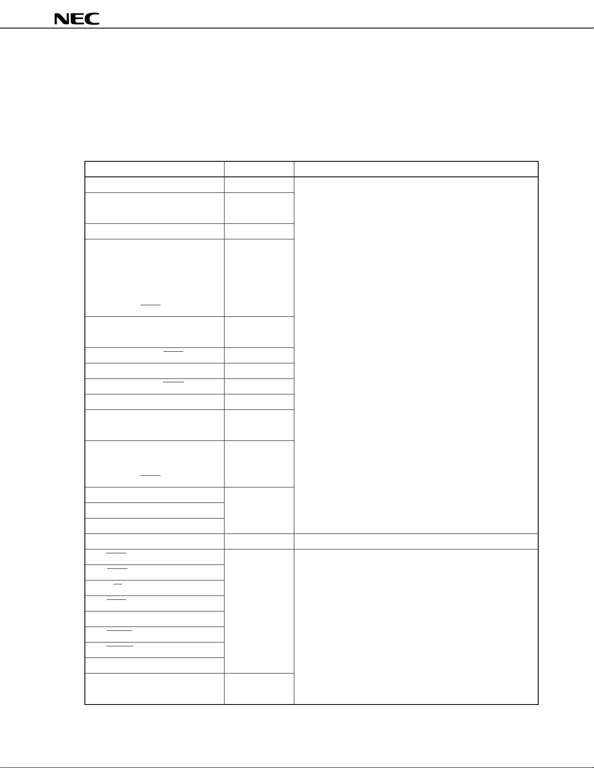
Pin Name I/O Function Shared with:
SCK0 I/O Serial clock I/O of CSI0-CSI3 (3 wire) P24
SCK1 P27
SCK2 P17/INTP123
SCK3 P37/INTP133
TXD0 Output Serial transmit data output of UART0-UART1 P22/SO0
TXD1 P25/SO1
RXD0 Input Serial receive data input of UART0-UART1 P23/SI0
RXD1 P26/SI1
PWM0 Output Pulse signal output of PWM P20
PWM1 P21
AD0-AD7 I/O 16-bit multiplexed address/data bus when external memory is connected P40-P47
AD8-AD15 P50-P57
A16-A19 Output High-order address bus when external memory is connected P60-P63
LBEN Output Low-order byte enable signal output of external data bus P90
UBEN High-order byte enable signal output of external data bus P91
R/W Output External read/write status output P92
DSTB External data strobe signal output P93
ASTB External address strobe signal output P94
HLDAK Output Bus hold acknowledge output P95
HLDRQ Input Bus hold request input P96
ANI0-ANI7 Input Analog input to A/D converter P70-P77
ANO0, ANO1 Output Analog output of D/A converter —
NMI Input Non-maskable interrupt request input —
CLKOUT Output System clock output —
CKSEL Input Input specifying operation mode of clock generator CVDD
WAIT Input Control signal input inserting wait state in bus cycle —
MODE Input Operation mode specification —
RESET Input System reset input —
X1 Input System clock resonator connection. Input external clock to X1 to —
X2 — supply external clock. —
ADTRG Input A/D converter external trigger input P07/INTP113
AVREF1 Input Reference voltage input for A/D converter —
AVREF2 Input Reference voltage input for D/A converter —
AVREF3 —
AVDD — Positive power supply for A/D converter —
AVSS — Ground potential for A/D converter —
CVDD — Positive power supply for internal clock generator CKSEL
CVSS — Ground potential for internal clock generator —
VDD — Positive power supply —
VSS — Ground potential —
VPP — High voltage application pin when program is written/verified —
(2/2)
10
Data Sheet U13189EJ3V0DS00
µ
PD70F3003A, 70F3025A
2.3 I/O Circuits of Pins and Recommended Connections of Unused Pins
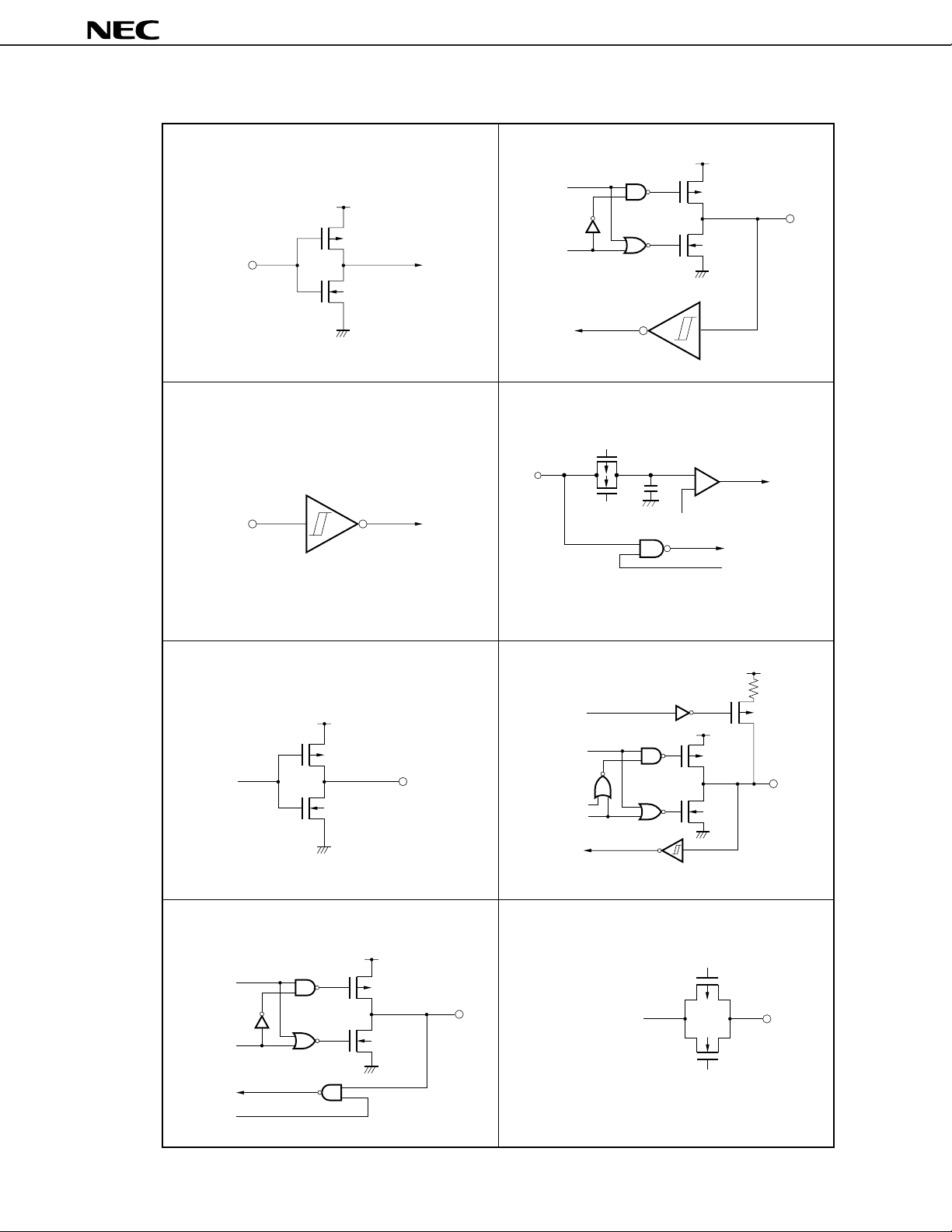
Table 2-1 shows the I/O circuit type of each pin, and the recommended connections of the unused pins. Figure
2-1 shows a partially simplified diagram of each circuit.
When connecting a pin to VDD or VSS via resistor, use of a resistor of 1 to 10 kΩ is recommended.
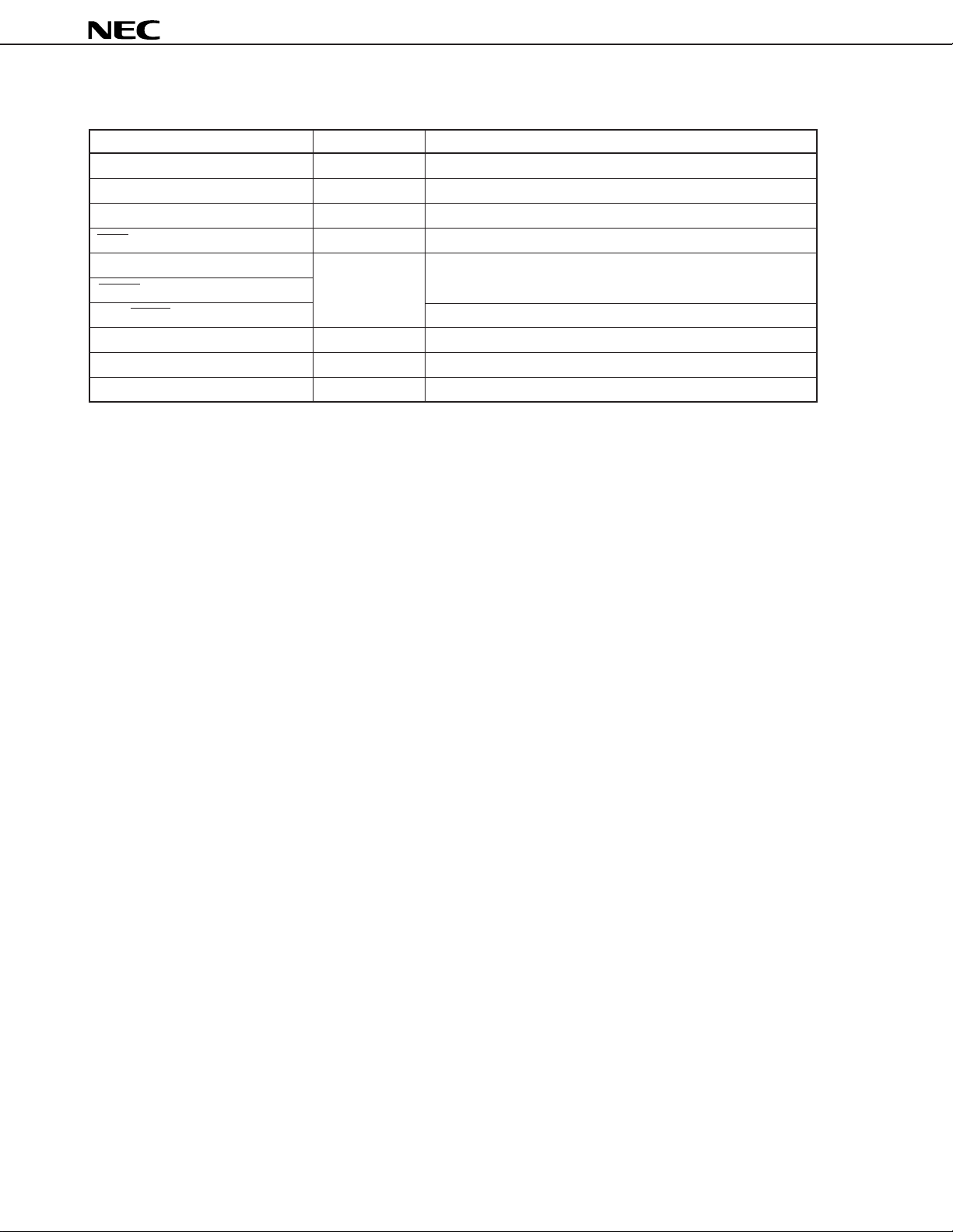
Table 2-1. I/O Circuit Types of Each Pin and Recommended Connections of Unused Pins (1/2)
Pin I/O Circuit Type Recommended Connections
P00/TO110, P01/TO111 5 Input : Individually connect to VDD or VSS via resistor.
P02/TCLR11, P03/TI11, 8 Output : Leave unconnected.
P04/INTP110-P07/INTP113/ADTRG
P10-TO120, P11/TO121 5
P12/TCLR12, P13/TI12 8
P14/INTP120
P15/INTP121/SO2
P16/INTP122/SI2
P17/INTP123/SCK2
P20/PWM0, P21/PWM1 5
P22/TXD0/SO0
P23/RXD0/SI0, P24/SCK0 8
P25/TXD1/SO1 5
P26/RXD1/SI1, P27/SCK1 8
P30/TO130, P31/TO131 5
P32/TCLR13, P33/TI13 8
P34/INTP130
P35/INTP131/SO3 10-A
P36/INTP132/SI3
P37/INTP133/SCK3
P40/AD0-P47/AD7 5
P50/AD8-P57/AD15
P60/A16-P63/A19
P70/ANI0-P77/ANI7 9 Directly connect to VSS.
P90/LBEN 5 Input: Individually connect to VDD or VSS via resistor.
P91/UBEN Output: Leave unconnected.
P92/R/W
P93/DSTB
P94/ASTB
P95/HLDAK
P96/HLDRQ
P110/TO140, P111/TO141
P112/TCLR14, P113/TI14 8
P114/INTP140-P117/INTP143
Data Sheet U13189EJ3V0DS00
11
µ
PD70F3003A, 70F3025A
Table 2-1. I/O Circuit Types of Each Pin and Recommended Connections of Unused Pins (2/2)
Pin I/O Circuit Type Recommended Connections
ANO0, ANO1 12 Leave unconnected.
NMI 2 Directly connect to VSS.
CLKOUT 3 Leave unconnected.
WAIT 1 Directly connect to VDD.
MODE 2
RESET
CVDD/CKSEL —
AVREF1-AVREF3, AVSS — Directly connect to VSS.
AVDD — Directly connect to VDD.
VPP — Connect to VSS.
—
12
Data Sheet U13189EJ3V0DS00
µ
Figure 2-1. I/O Circuits of Pins
PD70F3003A, 70F3025A
Type 1
Type 2
Type 8
V
DD
V
DD
P-ch
IN
Data
Output
disable
P-ch
IN/OUT
N-ch
N-ch
Type 9
P-ch
Comparator
IN
N-ch
IN
+
–
V
REF
(Threshold voltage)
Input enable
Schmitt trigger input with hysteresis characteristics
Type 3
V
DD
P-ch
OUT
N-ch
Type 5
V
DD
Data
Output
disable
P-ch
N-ch
IN/OUT
Type 10-A
Pullup
enable
Data
Open drain
Output disable
Type 12
Analog output voltage
P-ch
N-ch
V
DD
P-ch
V
DD
P-ch
IN/OUT
N-ch
OUT
Input
enable
Data Sheet U13189EJ3V0DS00
13
µ
PD70F3003A, 70F3025A
3. ELECTRICAL SPECIFICATIONS
3.1 Normal Operation Mode
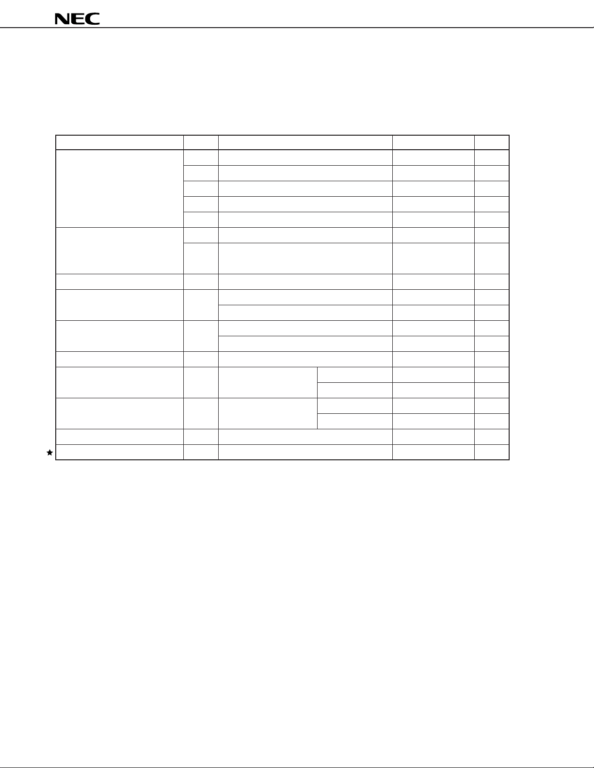
Absolute Maximum Ratings (TA = 25°C)
Parameter Symbol Condition Ratings Unit
Supply voltage VDD VDD pin –0.5 to +7.0 V
CVDD CVDD pin –0.5 to VDD + 0.3 V
CVSS CVSS pin –0.5 to +0.5 V
AVDD AVDD pin –0.5 to VDD + 0.3 V
AVSS AVSS pin –0.5 to +0.5 V
Input voltage VI1 Note, VDD = 5.0 V ± 10% –0.5 to VDD + 0.3 V
VI2 VPP pin in flash memory programming mode, –0.5 to +11.0 V
VDD = 5.0 V ± 10%
Clock input voltage VK X1 pin, VDD = 5.0 V ± 10% –0.5 to VDD + 1.0 V
Output current, low ICL 1 pin 4.0 mA
Total of all pins 100 mA
Output current, high ICH 1 pin –4.0 mA
Total of all pins –100 mA
Output voltage VO VDD = 5.0 V ± 10% –0.5 to VDD + 0.3 V
Analog input voltage VIAN P70/ANI0-P77/ANI7 AVDD > VDD –0.5 to VDD + 0.3 V
VDD ≥ AVDD –0.5 to AVDD + 0.3 V
Analog reference input voltage AVREF AVREF1-AVREF3 AVDD > VDD –0.5 to VDD + 0.3 V
VDD ≥ AVDD –0.5 to AVDD + 0.3 V
Operating ambient temperature TA –40 to +85 °C
Storage temperature Tstg –65 to +125 °C
Note Except X1, P70/AN0-P77/AN7, AVREF1-AVREF3
Cautions 1. Do not directly connect the output (or I/O) pins of two or more IC products, and do not directly
connect them to VDD, VCC, or GND pin. Open-drain pins and open-collector pins may be directly
connected to one another however. Moreover, an external circuit that is designed to prevent
contention of output can be connected to pins that go into a high-impedance state.
2. Should the absolute maximum rating of even one of the above parameters be exceeded even
momentarily, the quality of the program may be degraded. The absolute maximum ratings
are, therefore, the values exceeding which the product may be physically damaged. Use the
product so that these values are never exceeded.
The normal operating ranges of ratings and conditions in which the quality of the product
is guaranteed are specified in the following DC Characteristics and AC Characteristics.
14
Data Sheet U13189EJ3V0DS00
 Loading...