NEC UPD705102GM-143-8ED, UPD705102GM-133-8ED Datasheet
DATA SHEET
MOS INTEGRATED CIRCUIT
µ
PD705102
V832
TM
32-BIT MICROPROCESSOR
DESCRIPTION
The µPD705102 (V832) is a 32-bit RISC microprocessor for embedded control applications, with a highperformance 32-bit V830TM processor core and many peripheral functions such as a SDRAM/ROM controller, 4channel DMA controller, real-time pulse unit, serial interface, interrupt controller, and power management.
In addition to high interrupt response speed and optimized pipeline structure, the V832 offers sum-of-products
operation instructions, concatenated shift instructions, and high-speed branch instructions to realize multimedia
functions, and therefore can provide high performance in multimedia systems such as Internet/intra-net systems, car
navigation systems, digital still cameras, and color faxes.
Detailed function descriptions are provided in the following user’s manuals. Be sure to read them before
designing.
V832 User’s Manual — Hardware: U13577E
TM
V830 Family
FEATURES
• CPU function
• V830-compatible instructions
• Instruction cache: 4 Kbytes
• Instruction RAM: 4 Kbytes
• Data cache: 4 Kbytes
• Data RAM: 4 Kbytes
• Minimum number of instruction
execution cycles: 1 cycle
• Number of general purpose
registers: 32 bits × 32
• Memory space and I/O space: 4 Gbytes each
• Interrupt/exception processing function
• Non-maskable: External input: 1
• Maskable: External input: 8 (of which 4 are
Internal source: 11 types
• Bus control function
• Wait control function
• Memory access control function
User’s Manual — Architecture: U12496E
• DMA controller: 4 channels
• Serial interface function
• Asynchronous serial interface (UART): 1 channel
• Clocked serial interface (CSI): 1 channel
• Dedicated baud rate generator (BRG): 1 channel
• Timer/counter function
• 16-bit timer/event counter: 1 channel
• 16-bit interval timer: 1 channel
• Port function: 21 I/O ports
• Clock generation function: PLL clock synthesizer (6× or
8× multiplication)
• Standby function: HALT, STOP, and power management modes
• Debug function
multiplexed with
internal sources)
• Debug-dedicated synchronous serial
interface: 1 channel
• Trace-dedicated interface: 1 channel
The information in this document is subject to change without notice. Before using this document, please
confirm that this is the latest version.
Not all devices/types available in every country. Please check with local NEC representative for availability
and additional information.
Document No. U13675EJ2V1DS00 (2nd edition)
Date Published July 1999 N CP(K)
Printed in Japan
The mark shows major revised points.
©
1999
ORDERING INFORMATION
Part Number Package
µ
PD705102GM-143-8ED 160-pin plastic LQFP (fine pitch) (24 × 24 mm)
µ
PD705102GM-133-8ED 160-pin plastic LQFP (fine pitch) (24 × 24 mm)
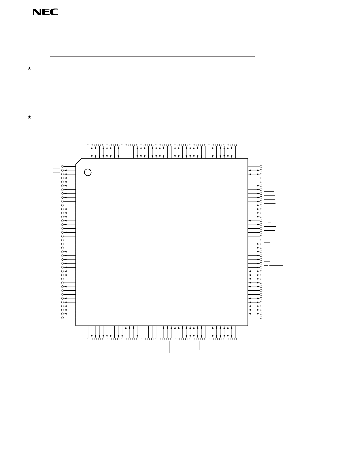
PIN CONFIGURATION (TOP VIEW)
• 160-pin plastic LQFP (fine pitch) (24 × 24 mm)
µ
PD705102GM-143-8ED
µ
PD705102GM-133-8ED
µ
PD705102
GND_O
CS1
CS0
WE
RAS
UUDQM
ULDQM
LUDQM
LLDQM
DD
_O
V
GND_O
SDCLKOUT
CKE
CAS
DD
V
GND_I
DD
_O
V
GND_O
A10
A11
DD
_O
V
GND_O
A12
A13
A14
A15
A16
A17
A18
A19
DD
_O
V
_O
DD
D31
D30
D29
D28
159
158
157
156
D27
155
V
160
1
2
3
4
5
6
7
8
9
10
11
12
13
A1
A2
A3
A4
_I
A5
A6
A7
A8
A9
14
15
16
17
18
19
20
21
22
23
24
25
26
27
28
29
30
31
32
33
34
35
36
37
38
39
40
414243444546474849505152535455565758596061626364656667686970717273747576777879
D26
154
D25
153
D24
152
_I
DD
GND_I
V
151
150
_O
DD
GND_O
V
D23
149
148
147
D22
146
D21
145
D20
144
D19
143
D18
142
D17
141
D16
GND_O
140
139
_O
DD
V
138
D15
137
D14
136
D13
135
D12
134
D11
133
D10D9D8
132
131
_O
DD
GND_O
V
D7D6D5D4D3D2GND_I
130
129
128
127
126
125
124
123
122
121
80
120
119
118
117
116
115
114
113
112
111
110
109
108
107
106
105
104
103
102
101
100
V
DD
_I
D1
D0
GND_O
_
O
DD
V
MRD
MWR
LLBEN
LUBEN
ULBEN
UUBEN
IOWR
IORD
BCYST
READY
R/W
HLDRQ
HLDAK
GND_O
_
O
DD
V
CS2
99
98
97
96
95
94
93
92
91
90
89
88
87
86
85
84
83
82
81
CS3
CS4
CS5
CS6
CS7
TC/STOPAK
PORTA1/DMAAK0
PORTA3/DMAAK1
PORTA5/DMAAK2
PORTA7/DMAAK3
PORTA0/DMARQ0
PORTA2/DMARQ1
PORTA4/DMARQ2
PORTA6/DMARQ3
PORTB7/INTP03
PORTB6/INTP02
PORTB4/INTP01
PORTB2/INTP00
GND_I
A20
A21
GND_O
A22
A23
CLKOUT
TRCDATA0
TRCDATA1
TRCDATA2
TRCDATA3
DDI
DCK
DMS
DDO
_PLL
DD
V
X2
GND_PLL
DD
V
IC1
GND_I
BT16B
RESET
NMI
DRST
CMODE
PORT3/RXD
PORT2/SI
PORT1/SO
PORT4/TXD
PORT0/SCLK
_O
DD
V
GND_O
_I
X1
Caution Directly connect the IC1 (Internally connected 1) pin to GND_O.
2
Data Sheet U13675EJ2V1DS00
PORTB0/TI
INTP10/TO10
INTP12/TO11
PORTB5/INTP11
PORTB3/INTP13
_I
DD
V
PORTB1/TCLR
PIN NAMES
µ
PD705102
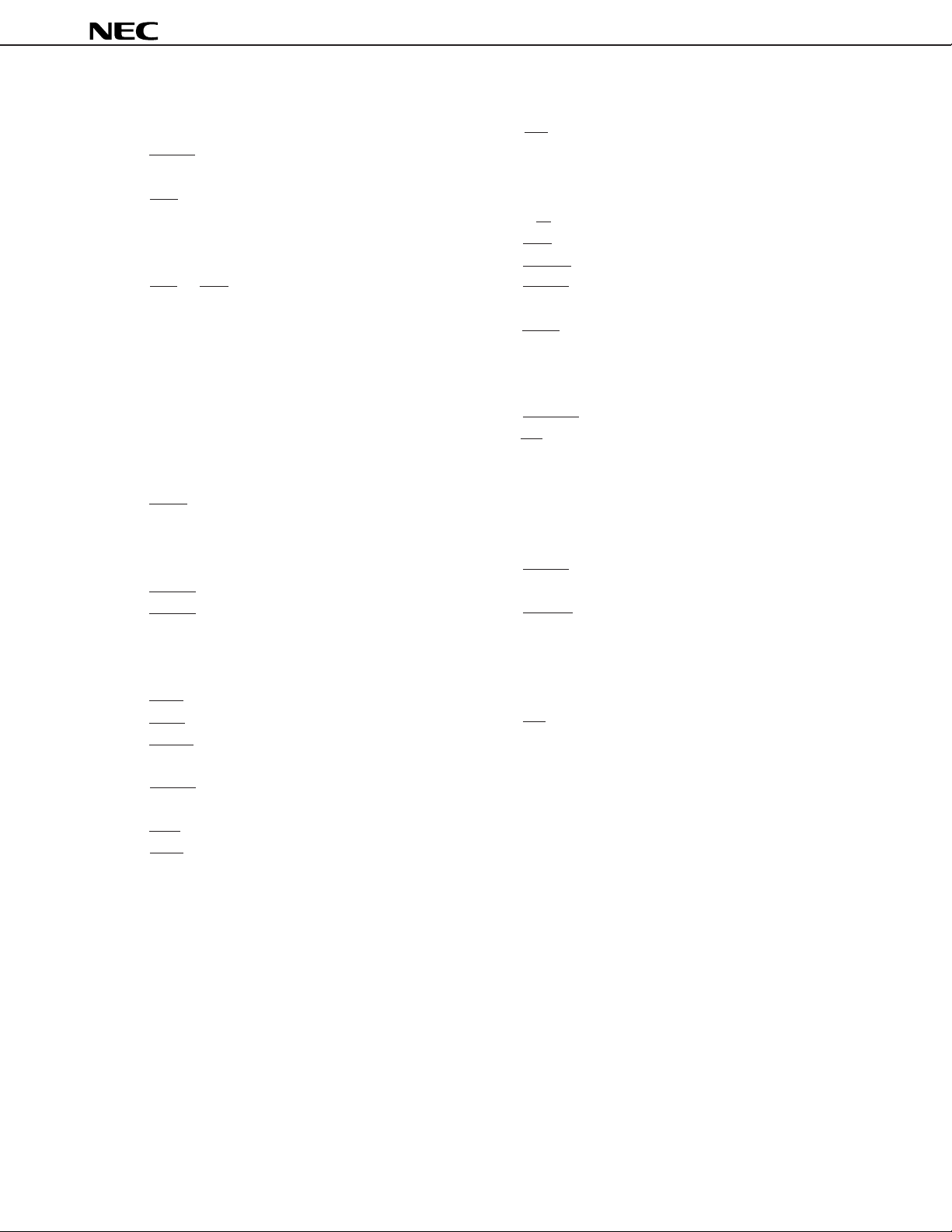
A1 to A23: Address Bus
BCYST: Bus Cycle Start
BT16B: Boot Bus Size 16-bit
CAS: Column Address Strobe
CKE: Clock Enable
CLKOUT: Clock Out
CMODE: Clock Mode
CS0 to CS7: Chip Select
D0 to D31: Data Bus
DCK: Debug Clock
DDI: Debug Data Input
DDO: Debug Data Output
DMAAK0 to DMAAK3:
DMA Acknowledge
DMARQ0 to DMARQ3:
DMA Request
DMS: Debug Mode Select
DRST: Debug Reset
GND_I: Ground
GND_O: Ground
GND_PLL: PLL Ground
HLDAK: Hold Acknowledge
HLDRQ: Hold Request
IC1: Internally Connected
INTP00 to INTP03, INTP10 to INTP13:
Interrupt Request From Peripheral
IORD: I/O Read
IOWR: I/O Write
LLBEN: Lower Lower Byte Enable
LLDQM: Lower Lower DQ Mask enable
LUBEN: Lower Upper Byte Enable
LUDQM: Lower Upper DQ Mask enable
MRD: Memory Read
MWR: Memory Write
NMI: Non-Maskable Interrupt Request
PORT0 to PORT4,
PORTA0 to PORTA7,
PORTB0 to PORTB7: Port
R/W: Bus Read or Write Status
RAS: Row Address Strobe
READY: Ready
RESET: Reset
RXD: Receive Data
SCLK: Serial Clock
SDCLKOUT: SDRAM Clock Out
SI: Serial Input
SO: Serial Output
STOPAK: Stop Acknowledge
TC: Terminal Count
TCLR: Timer Clear
TI: Timer Input
TO10, TO11: Timer Output
TRCDATA0 to TRCDATA3: Trace Data
TXD: Transmit Data
ULBEN: Upper Lower Byte Enable
ULDQM: Upper Lower DQ Mask enable
UUBEN: Upper Upper Byte Enable
UUDQM: Upper Upper DQ Mask enable
DD_I: Power Supply (2.5 V)
V
DD_O: Power Supply (3.3 V)
V
VDD_PLL: PLL Power Supply (2.5 V)
WE: Write Enable
X1, X2: Crystal Oscillator
3Data Sheet U13675EJ2V1DS00
INTERNAL BLOCK DIAGRAM
µ
PD705102
DCK
DMS
DDI
DDO
TRCDATA3 to TRCDATA0
DRST
X1
X2
CLKOUT
SDCLKOUT
RESET
NMI
TI, TCLR
INTP10/TO10,
INTP12/TO11
INTP11, INTP13
INTP00 to INTP03
SCLK
SO
TXD
RXD
R/W
IOWR
DCU
CG
BCU
SYU
RPU
ICU
PIO
CSI
SI
V830 core
BRG
UART
DMAC
IORD
MWR
MRD
UUBEN, ULBEN, LUBEN, LLBEN
READY
BT16B
BCYST
CS7 to CS0
A23 to A1
D31 to D0
HLDRQ
HLDAK
RAS
CAS
UUDQM, ULDQM, LUDQM, LLDQM
CKE
WE
STOPAK
CMODE
TC
DMARQ3 to DMARQ0
DMAAK3 to DMAAK0
4
Data Sheet U13675EJ2V1DS00

µ
PD705102
CONTENTS
1. PIN FUNCTIONS .................................................................................................................................. 6
1.1 Port Pins ....................................................................................................................................................... 6
1.2 Non-Port Pins ...............................................................................................................................................7
2. INTERNAL UNITS ................................................................................................................................ 9
3. CPU FUNCTION................................................................................................................................. 11
4. INTERRUPT/EXCEPTION PROCESSING FUNCTION ..................................................................... 12
5. BUS CONTROL FUNCTION .............................................................................................................. 14
6. WAIT CONTROL FUNCTION ............................................................................................................. 14
7. MEMORY ACCESS CONTROL FUNCTION ...................................................................................... 15
7.1 SDRAM Control Function .......................................................................................................................... 15
7.2 Page-ROM Control Function ..................................................................................................................... 17
8. DMA FUNCTION ................................................................................................................................ 18
9. SERIAL INTERFACE FUNCTION ...................................................................................................... 20
9.1 Asynchronous Serial Interface (UART)....................................................................................................20
9.2 Clocked Serial Interface (CSI) ................................................................................................................... 22
9.3 Baud Rate Generator (BRG)......................................................................................................................23
10. TIMER/COUNTER FUNCTION .......................................................................................................... 24
11. PORT FUNCTION .............................................................................................................................. 27
12. CLOCK GENERATION FUNCTION ................................................................................................... 32
13. STANDBY FUNCTION ....................................................................................................................... 33
14. RESET/NMI CONTROL FUNCTION .................................................................................................. 35
15. INSTRUCTIONS ................................................................................................................................. 36
15.1 Instruction Format .....................................................................................................................................36
15.2 Instructions (Listed Alphabetically) ......................................................................................................... 38
16. ELECTRICAL SPECIFICATIONS ...................................................................................................... 48
17. PACKAGE DRAWING ........................................................................................................................ 75
18. RECOMMENDED SOLDERING CONDITIONS ................................................................................. 76
5Data Sheet U13675EJ2V1DS00

1. PIN FUNCTIONS
1.1 Port Pins
Pin Name I/O Function Alternate Function
PORT0 Schmitt I/O PORT SCLK
PORT1 I/O
PORT2 Schmitt I/O
PORT3 RXD
PORT4 I/O TXD
PORTA0 I/O PORTA DMARQ0
PORTA1
PORTA2
PORTA3 DMAAK1
PORTA4 DMARQ2
PORTA5 DMAAK2
PORTA6 DMARQ3
PORTA7 DMAAK3
PORTB0 I/O PORTB TI
PORTB1
PORTB2
PORTB3 INTP13
PORTB4 INTP01
PORTB5 INTP11
PORTB6 INTP02
PORTB7 INTP03
5-bit input/output port.
Input/output can be specified in 1-bit units.
8-bit input/output port.
Input/output can be specified in 1-bit units.
8-bit input/output port.
Input/output can be specified in 1-bit units.
SO
SI
DMAAK0
DMARQ1
TCLR
INTP00
µ
PD705102
6
Data Sheet U13675EJ2V1DS00
µ
PD705102
1.2 Non-Port Pins
Pin Name I/O Function Alternate Function
D0 to D31 3-state I/O Data bus —
A1 to A23 3-state output Address bus —
READY Input End of bus cycle enable —
HLDRQ Input Bus hold request —
HLDAK Output Bus hold enable —
MRD 3-state output Memory read strobe —
UUBEN Byte enable output (most significant byte: D31 to D24) —
ULBEN Byte enable output (enables second byte: D23 to D16) —
LUBEN Byte enable output (enables third byte: D15 to D8) —
LLBEN Byte enable output (enables least significant byte: D7 to D0) —
IORD I/O read strobe —
IOWR I/O write strobe —
MWR Memory write strobe —
BT16B Input CS7 space bus size setting —
BCYST 3-state output Bus cycle start output —
R/W R/W output —
RESET Input Reset input —
X1 — Crystal resonator connection (open when external clock input) —
X2 Schmitt input Crystal resonator connection/external clock input —
CLKOUT Output Bus clock output —
CMODE Input PLL multiplication factor setting (×6, ×8) —
CS2, CS7 3-state output Memory chip select output —
CS3 to CS6 Memory I/O chip select output —
STOPAK Output STOP mode report output TC
INTP10 Input Maskable interrupts TO10
INTP11 PORTB5
INTP12 TO11
INTP13 PORTB3
INTP00 PORTB2
INTP01 PORTB4
INTP02 PORTB6
INTP03 PORTB7
NMI Non-maskable interrupt —
RAS 3-state output SDRAM RAS strobe —
UUDQM DQ mask enable (most significant byte: D31 to D24) —
ULDQM DQ mask enable (second byte: D23 to D16) —
LUDQM DQ mask enable (third byte: D15 to D8) —
LLDQM DQ mask enable (least significant byte: D7 to D0) —
(1/2)
7Data Sheet U13675EJ2V1DS00
µ
Pin Name I/O Function Alternate Function
WE 3-state output SDRAM write strobe —
CAS SDRAM CAS strobe —
CS0 SDRAM chip select —
CS1 SDRAM/SRAM (ROM) chip select —
CKE SDRAM clock enable —
SDCLKOUT Output SDRAM clock output —
DMARQ0 Input DMA requests (CH0 to CH3) PORTA1
DMARQ1 PORTA3
DMARQ2 PORTA5
DMARQ3 PORTA7
DMAAK0 Output DMA enable (CH0 to CH3) PORTA0
DMAAK1 PORTA2
DMAAK2 PORTA4
DMAAK3 PORTA6
TC DMA transfer end output STOPAK
TO10 Timer 1 output INTP10
TO11 INTP12
TCLR Input Timer 1 clear, start input PORTB1
TI Timer 1 count clock input PORTB0
RXD Schmitt input UART data input PORT3
TXD Output UART data output PORT4
SCLK Schmitt I/O CSI clock I/O PORT0
SI Schmitt input CSI data input PORT2
SO Output CSI data output PORT1
DCK Schmitt input Debug clock input —
DDI Input Debug data input —
DDO Output Debug data output —
DMS Input Debug mode select —
DRST DCU reset input —
TRCDATA0 to Output Trace data output —
TRCDATA3
VDD_I — Positive power supply (2.5 V) —
VDD_O Positive power supply (3.3 V) —
GND_I Ground (2.5 V) —
GND_O Ground (3.3 V) —
VDD_PLL PLL (internal clock generator) positive power supply (2.5 V) —
GND_PLL PLL (internal clock generator) ground potential (2.5 V) —
PD705102
(2/2)
8
Data Sheet U13675EJ2V1DS00

µ
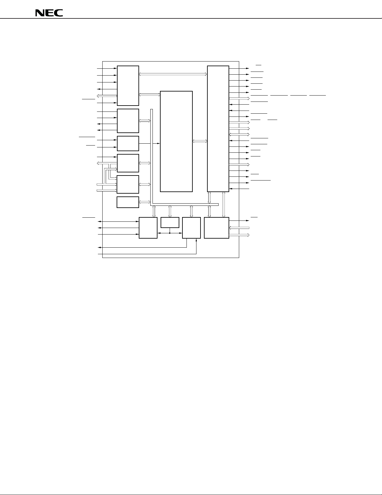
2. INTERNAL UNITS
(1) Bus control unit (BCU)
Controls the address bus, data bus, and control bus pins. The major functions of BCU are as follows:
(a) Bus arbitration
Arbitrates the bus mastership among bus masters (CPU, SDRAMC, DMAC, and external bus masters). The
bus mastership can be changed after completion of the bus cycle under execution, and in an idle state.
(b) Wait control
Controls eight areas in the 16-Mbyte space corresponding to eight chip select signals (CS0 through CS7).
Generates chip select signals, controls wait states, and selects the type of bus cycle.
(c) SDRAM controller
Generates commands and controls access to SDRAM. CAS latency is 2 only.
(d) ROM controller
Accessing ROM with page access function is supported. The bus cycle immediately before and addresses
are compared, and wait states are controlled in the normal access (off-page) or page access (on-page)
modes. A page width of 8 bytes to 16 bytes can be supported.
PD705102
(2) Interrupt controller (ICU)
Services maskable interrupt requests (INTP00 through INTP03, and INTP10 through INTP13) from internal
peripheral hardware and external sources. The priorities of these interrupt requests can be specified in units of
four groups, and edge-triggered or level-triggered interrupts can be nested.
(3) DMA controller (DMAC)
Transfers data between memory and I/O in place of CPU. The transfer type is 2-cycle transfer. Two transfer
modes, single transfer and demand transfer, are available.
(4) Serial interface (UART/CSI/BRG)
One asynchronous serial interface (UART) channel and one clocked serial interface (CSI) channel is provided.
As the serial clock source, the output of the baud rate generator (BRG) and the bus clock can be selected.
(5) Real-time pulse unit (RPU)
Provides timer/counter functions. The on-chip 16-bit timer/event counter and 16-bit interval timer can be used
to calculate pulse intervals and frequencies, and to output programmable pulses.
(6) Clock generator (CG)
A frequency six or eight times higher than that of the resonator connected to the X1 and X2 pins is supplied as
the operating clock of the CPU. In addition, both a bus clock, which functions as the operating clock of the
peripheral units, and SDCLKOUT, which functions as an operating clock, are supplied from the CLKOUT pin. An
external clock can be also input instead of connecting a resonator.
For reducing the power consumption, the function switching the frequencies of the CPU clock and bus clock with
power management control (PMC) is provided.
9Data Sheet U13675EJ2V1DS00

µ
(7) Port (PIO)
Provides port functions. Twenty-one I/O ports are available. The pins of these ports can be used as port pins
or other function pins.
(8) System control unit (SYU)
A circuit that eliminates noise on the RESET signal (input)/NMI signal (input) is provided.
(9) Debug control unit (DCU)
A circuit to realize mapping and trace functions is provided to implement basic debugging functions.
PD705102
10
Data Sheet U13675EJ2V1DS00

3. CPU FUNCTION
The features of the CPU function are as follows:
• High-performance 32-bit architecture for embedded control applications
• Cache memory
Instruction cache: 4 Kbytes
Data cache: 4 Kbytes
• Internal RAM
Instruction RAM: 4 Kbytes
Data RAM: 4 Kbytes
• 1-clock pitch pipeline structure
• 16-/32-bit length instruction format
• Address/data separated type bus
• 4-Gbyte linear address
• Thirty-two 32-bit general registers
• Register/flag hazard interlock is handled by hardware
• 16 levels of interrupt response
• 16-bit bus fixed function
• 16-bit bus system can be constructed
• Ideal instructions for any application field:
• Sum-of-products operation
• Saturation operation
• Branch prediction
• Concatenation shift
• Block transfer instruction
µ
PD705102
11Data Sheet U13675EJ2V1DS00
4. INTERRUPT/EXCEPTION PROCESSING FUNCTION
The features of the interrupt/exception processing function are as follows:
• Interrupt
• Non-maskable interrupt: 1 source
• Maskable interrupt: 15 sources
• Priority of the programmable interrupt can be specified in four levels
• Nesting interrupt can be controlled according to the priority
• Mask can be specified for each maskable interrupt request
• Valid edge of an external interrupt request can be specified
• Noise elimination circuit provided for the non-maskable interrupt pin (NMI)
• Exception
• Software exception: 32 sources
• Exception trap: 4 sources
The interrupt/exception sources are shown in Tables 4-1 and 4-2.
Table 4-1. Reset/Non-maskable Interrupt/Exception Source List
µ
PD705102
Type Classification Source of Interrupt/Exception Exception Code Handler Restore
Note 1
Name
Reset Interrupt RESET Reset input FFF0H FFFFFFF0H Undefined
Non-maskable Interrupt NMI NMI input FFD0H FFFFFFD0H next PC
Software exception Exception TRAP 1nH TRAP instruction FFBnH FFFFFFB0H next PC
TRAP 0nH TRAP instruction FFAnH FFFFFFA0H
Exception trap Exception NMI Dual exception Note 4 FFFFFFD0H current PC
FAULT Fatal exception Not affected FFFFFFE0H
I-OPC Illegal instruction FF90H FFFFFF90H
DIV0 Zero division FF80H FFFFFF80H
Cause
code
(ECR) Address PC
Note 2
Note 3
Notes 1. Handler names used in development tools or software.
2. The PC value saved to EIPC/FEPC/DPC when interrupt/exception processing is started.
3. Execution of all instructions cannot be stopped by an interrupt.
4. The exception code of an exception causing a dual exception.
Remark n = 0H to FH
12
Data Sheet U13675EJ2V1DS00
Table 4-2. Maskable Interrupt List
µ
PD705102
Type Classifi- Group In-Group Interrupt Source Exception Handler Address
cation Priority
Mask-
Interrupt
able
GR3 3 RESERVED Reserved — FEF0H FFFFFEF0H FE0000F0H next
GR2 3 INTSR UART receive end UART FEB0H FFFFFEB0H FE0000B0H
GR1 3 INTDMA DMA transfer end DMAC FE70H FFFFFE70H FE000070H
GR0 3 INTCM4 Coincidence of CM4 RPU FE30H FFFFFE30H FE000030H
Name Cause Unit
2 INTOV1 Timer 1 overflow RPU FEE0H FFFFFEE0H FE0000E0H
1 INTSER UART receive error UART FED0H FFFFFED0H FE0000D0H
0 INTP03 INTP03 pin input External FEC0H FFFFFEC0H FE0000C0H
2 INTST UART transmit end UART FEA0H FFFFFEA0H FE0000A0H
1 INTCSI CSI transmit/receive end CSI FE90H FFFFFE90H FE000090H
0 INTP02 INTP02 pin input External FE80H FFFFFE80H FE000080H
2 INTP10/ INTP10 pin input/ External/ FE60H FFFFFE60H FE000060H
INTCC10 coincidence of CC10 RPU
1 INTP11/ INTP11 pin input/ External/ FE50H FFFFFE50H FE000050H
INTCC11 coincidence of CC11 RPU
0 INTP01 INTP01 pin input External FE40H FFFFFE40H FE000040H
2 INTP12/ INTP12 pin input/ External/ FE20H FFFFFE20H FE000020H
INTCC12 coincidence of CC12 RPU
1 INTP13/ INTP13 pin input/ External/ FE10H FFFFFE10H FE000010H
INTCC13 coincidence of CC13 RPU
0 INTP00 INTP00 pin input External FE00H FFFFFE00H FE000000H
Code
HCCW.IHA=0 HCCW.IHA=1
Note 3
Restore
Note 1
PC
Note 2
PC
Notes 1. The PC value saved to EIPC when interrupt processing is started.
2. Execution of all instructions cannot be stopped by an interrupt.
3. FFFFFEn0H can be selected as a handler address when HCCW.IHA = 0, and FE0000n0H can be
selected when HCCW.IHA = 1 (n = 0H to FH).
Caution The exception codes and handler addresses of the maskable interrupts shown above are the
values if the default priority (IGP = E4H) is used. The correspondence between the interrupt
source and the handler address is changed from Table 4-2 if the priority of the group (GR0 to
GR3) is changed according to the value of the interrupt group priority register (IGP).
13Data Sheet U13675EJ2V1DS00

5. BUS CONTROL FUNCTION
The features of the bus control function are as follows:
• SDRAM, Page-ROM, SRAM (ROM) or I/O can be directly connected
• SDRAM read/write access with 1 bus clock minimum
• SDRAM byte access control with four ××DQM signals
• Wait control with READY signal
• RAM, ROM or I/O byte access control with four ××BEN signals
• 32-/16-bit bus width can be set every CS space
• When the 16-bit memory or I/O are accessed by data bus, the external data bus width can be set by the data
bus width control register (DBC).
Remarks 1. ××BEN: LLBEN, LUBEN, ULBEN, UUBEN
2. ××DQM: LLDQM, LUDQM, ULDQM, UUDQM
6. WAIT CONTROL FUNCTION
The features of the wait control function are as follows:
• Controls 8 blocks in accordance with I/O and memory spaces
• Linear address space of each block: 16 Mbytes
• Bus cycle select function
Block 0: SDRAM
Block 1: SDRAM, SRAM (ROM) selectable
Block 2: SRAM (ROM)
Blocks 3 through 6: I/O or SRAM (ROM) selectable
Block 7: Page-ROM or SRAM (ROM) selectable
• Data bus width select function
Data bus width selectable between 32 bits and 16 bits for each block
• Wait control function
Blocks 0 and 1: SDRAM wait control function is not provided
Blocks 1 through 4 and 7: 0 to 7 wait states
Blocks 5 and 6: 0 to 15 wait states
• Idle state insertion function
0 to 7 states for each block (bus clock)
µ
PD705102
14
Data Sheet U13675EJ2V1DS00

7. MEMORY ACCESS CONTROL FUNCTION
The features of the memory access control function are as follows:
• SDRAM control function
• Generates RAS, CAS, WE, CKE, LLDQM, LUDQM, ULDQM, and UUDQM signals
• Address multiplex: 8 or 9 bits
• Timing control of SDRAM access
Command interval from REF to REF/ACT: 3 to 6 bus clocks selectable
Command interval from ACT to PRE: 3 or 4 bus clocks selectable
Command interval from PRE to ACT: 1 or 2 bus clocks selectable
Command interval from ACT to READ/WRITE: 1 or 2 bus clocks selectable
CAS latency: 2 bus clocks fixed
• Auto refresh and self-refresh functions
• 8-bank control (4 banks × 2 blocks)
• Page-ROM control function
• Page size: 8 or 16 bytes
• Wait control during page access: 0 to 7 wait states
µ
PD705102
7.1 SDRAM Control Function
The BCU generates RAS, CAS, WE, CS0, CS1, CKE, LLDQM, LUDQM, ULDQM, and UUDQM signals and controls
access to the SDRAM. Addresses are output to the SDRAM from the address pins by multiplexing row and column
addresses.
The connected SDRAM must be of ×8 bits or more.
The refresh mode is a CAS-before-RAS (CBR) mode, and the refresh cycle can be arbitrarily set.
Self refresh is performed in the STOP mode.
(1) Address multiplex function
An address is multiplexed as shown in Tables 7-1 and 7-2 when row and column addresses are output in the
SDRAM cycle, depending on the values of the RAW and CAW bits of the SDRAM configuration register (SDC).
In the tables, a1 through a23 indicate the address output by the CPU, and A1 through A15 indicate the address
pins of the V832.
15Data Sheet U13675EJ2V1DS00
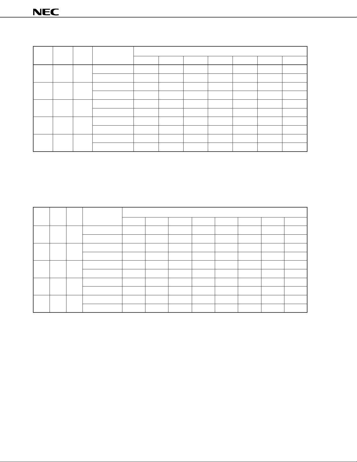
Table 7-1. Output of Row Address and Column Address (32-bit data width)
µ
PD705102
BAW RAW CAW Output Timing
0 00 00 Column address (a15) (a14) a21* AP (a11) (a10) a9 to a2
Row address a23 a22 a21* a20 a19 a18 a17 to a10
0 00 01 Column address (a15) (a14) a22* AP (a11) a10 a9 to a2
Row address (a15) a23 a22* a21 a20 a19 a18 to a11
1 00 00 Column address (a15) a22* a21* AP (a11) (a10) a9 to a2
Row address a23 a22* a21* a20 a19 a18 a17 to a10
1 00 01 Column address (a15) a23* a22* AP (a11) a10 a9 to a2
Row address (a15) a23* a22* a21 a20 a19 a18 to a11
1 01 00 Column address a23* a22* (a13) AP (a11) (a10) a9 to a2
Row address a23* a22* a21 a20 a19 a18 a17 to a10
A15 A14 A13 A12 A11 A10 A9 to A2
External Address Pin
Remarks 1. * indicates bank address specification.
2. AP is a bit used to specify a command and is fixed to low level.
3. Addresses in parentheses (a××) and A1 and A16 through A23 pins do not multiplex addresses and
always output the original values.
Table 7-2. Output of Row Address and Column Address (16-bit data width)
BAW RAW CAW Output Timing
0 00 00 Column address (a15) (a14) (a13) a20* AP (a10) (a9) a8 to a1
Row address a23 a22 a21 a20* a19 a18 a17 a16 to a9
0 00 01 Column address (a15) (a14) (a13) a21* AP (a10) a9 a8 to a1
Row address (a15) a23 a22 a21* a20 a19 a18 a17 to a10
1 00 00 Column address (a15) (a14) a21* a20* AP (a10) (a9) a8 to a1
Row address a23 a22 a21* a20* a19 a18 a17 a16 to a9
1 00 01 Column address (a15) (a14) a22* a21* AP (a10) a9 a8 to a1
Row address (a15) a23 a22* a21* a20 a19 a18 a17 to a10
1 01 00 Column address (a15) a22* a21* (a12) AP (a10) (a9) a8 to a1
Row address a23 a22* a21* a20 a19 a18 a17 a16 to a9
A15 A14 A13 A12 A11 A10 A9 A8 to A1
External Address Pin
Remarks 1. * indicates bank address specification.
2. AP is a bit used to specify a command and is fixed to low level.
3. Addresses in parentheses (a××) and A16 through A23 pins do not multiplex addresses and always
output the original values.
16
Data Sheet U13675EJ2V1DS00
µ
PD705102
(2) On-page/off-page decision
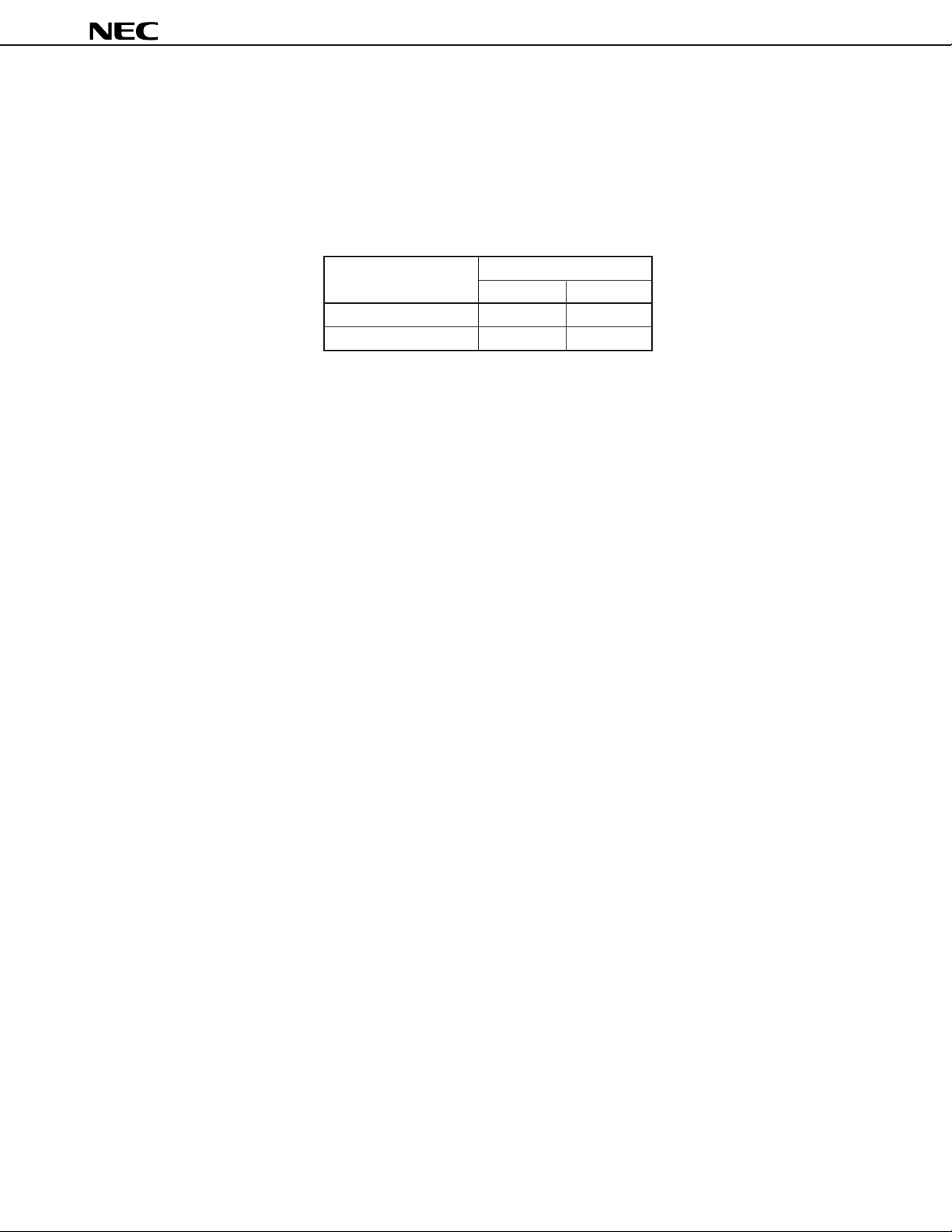
When the PAE bit of the SDRAM configuration register (SDC) is 1 (page access enabled), whether the SDRAM
access to be started is in the same page as the previous SDRAM access is decided. When the PAE bit is 0,
the off-page cycle is always started. Table 7-3 shows the relation between an address to be compared and address
shift.
Table 7-3. Address Compared by on-page/off-page Decision
Address Shift Data Bus Width
16 bits 32 bits
8 a23 to a9 a23 to a10
9 a23 to a10 a23 to a11
(3) Refresh function
The BCU can automatically generate the distributed auto refresh cycle necessary for refreshing the SDRAM.
Whether refreshing is enabled or disabled and the refresh interval are set by the refresh control register (RFC).
The BCU has a refresh request queue that can store refresh requests up to seven times.
7.2 Page-ROM Control Function
The BCU controls page access to the Page-ROM. Page access to the Page-ROM is valid during burst access.
The page size (8 bytes/16 bytes) and the number of wait states (0 wait/1 wait) during page access can be set by using
the Page-ROM configuration register (PRC).
17Data Sheet U13675EJ2V1DS00

8. DMA FUNCTION
The features of the DMA function are as follows:
• Four independent DMA channels
• Transfer unit: bytes, half words (2 bytes), words (4 bytes)
24
• Maximum number of transfers: 16,777,216 (2
• Transfer type: 2-cycle transfer
• Two transfer modes
• Single transfer mode
• Demand transfer mode
• Transfer request
• External DMARQ pin (×4)
• Request from internal peripheral hardware (serial interface (×3 channels) and timer)
• Request from software
• Transfer source and destination
• Between memory and I/O
• Between memory and memory
• Programmable wait function
• DMA transfer end signal output (TC)
) times
µ
PD705102
18
Data Sheet U13675EJ2V1DS00
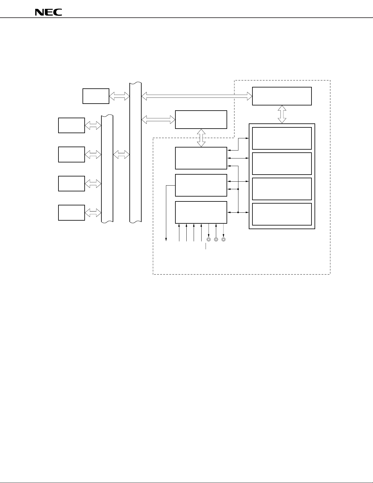
The configuration of the DMA controller (DMAC) is shown below.
Figure 8-1. Block Diagram of DMAC
DMAC
µ
PD705102
ROM
RAM
I/O
I/O
Internal I/O
External bus
Address control block
Internal peripheral I/O bus
Counter control block
Channel control block
INTSR
INTCM4
INTDMA
BCU
INTST
INTCSI
TC
DMAAK0 to 3
DMARQ0 to 3
Bus interface
DMA source address
register (DSA)
DMA destination address
register (DDA)
DMA transfer count
register (DBC)
DMA control register
(DCHC, DC)
19Data Sheet U13675EJ2V1DS00

9. SERIAL INTERFACE FUNCTION
The following channels are provided for the serial interface function.
• Asynchronous serial interface (UART): 1 channel
• Clocked serial interface (CSI): 1 channel
• Baud rate generator (BRG): 1 channel
9.1 Asynchronous Serial Interface (UART)
The features of the asynchronous serial interface (UART) are as follows:
• Full duplex communication. Receive buffer (RXB) is provided (transmit buffer (TXB) is not provided).
• Two-pin configuration (The UART of the V832 does not have the SCLK and CTS pins.)
• TXD: Transmit data output pin
• RXD: Receive data input pin
• Transfer rate: 300 bps to 153600 bps (bus clock: 47.6 MHz, with BRG)
: 150 bps to 76800 bps (bus clock: 35.7 MHz, with BRG)
• Baud rate generator
φ
Serial clock source can be selected from baud rate generator output or bus clock (
• Receive error detection function
• Parity error
• Framing error
• Overrun error
• Three interrupt sources
• Receive error interrupt (INTSER)
The interrupt request is generated by ORing three types of receive errors.
• Receive end interrupt (INTSR)
The receive end interrupt request is generated after completion of receive data transfer from the shift register
to the receive buffer in the reception enabled status.
• Transmit end interrupt (INTST)
The transmit end interrupt request is generated after completion of serial transfer of transmit data (9, 8, or
7 bits) from the shift register. The character length of the transmit/receive data is specified by the ASIM00
and ASIM01 registers.
• Character length: 7 or 8 bits
: 9 bits (with extension bit appended)
• Parity function: Odd, even, 0, or none
• Transmit stop bit: 1 or 2 bits
)
µ
PD705102
20
Data Sheet U13675EJ2V1DS00
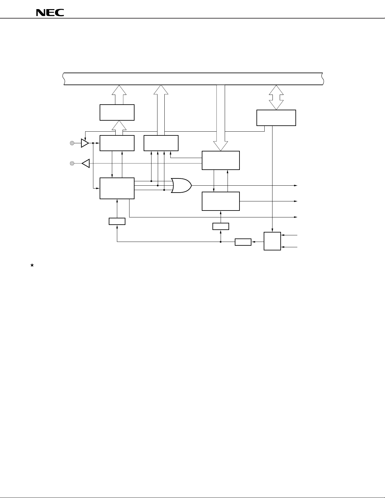
The configuration of the asynchronous serial interface (UART) is shown below.
Figure 9-1. Block Diagram of UART
Internal peripheral I/O bus
µ
PD705102
16/8
RXB0
RXD
TXD
RXB0L
Receive buffer
Receive shift
register
Receive
control parity
check
1/16
8
Status register
ASIS0
Transmit shift
register
Transmit control
parity append
Remarkφ = bus clock:48 M to 1.3 MHz: @input clock 6×
:36 M to 0.73 MHz: @input clock 8×
16/8
1/16
TXS0
TXS0L
1/2
8
Mode register
SEL
ASIM00
ASIM01
INTSER
INTST
INTSR
φ
Baud rate generator
21Data Sheet U13675EJ2V1DS00
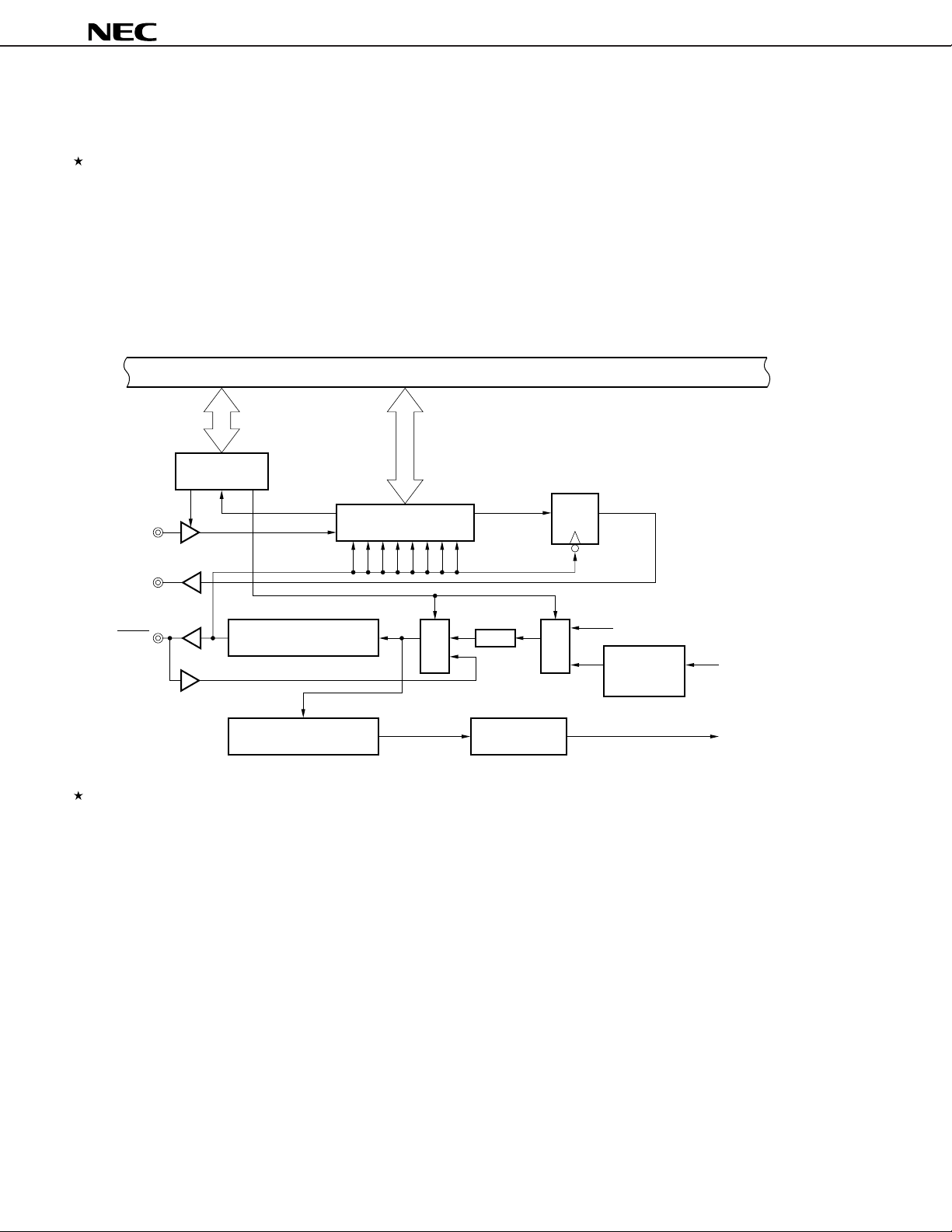
9.2 Clocked Serial Interface (CSI)
The features of the clocked serial interface (CSI) are as follows:
• High-speed transfer: 12.0 Mbps Max. (bus clock: 48.0 MHz)
• Half duplex communication for transmission/reception (buffer is not provided)
• Character length: 8 bits
• External or internal serial clock selectable
The configuration of the clocked serial interface (CSI) is shown below.
Figure 9-2. Block Diagram of CSI
Internal peripheral I/O bus
8
8
CSIM0
SI
Mode register
Shift register
SIO0
SO latch
DQ
µ
PD705102
SO
SCLK
Serial clock control circuit
Serial clock counter
SEL
Interrupt control
circuit
Remarkφ = bus clock:48 M to 1.3 MHz: @input clock 6×
:36 M to 0.73 MHz: @input clock 8×
1/2
SEL
Baud rate generator
1/2, 1/4, 1/8,
1/16, 1/32
prescaler
φ
INTCSI
22
Data Sheet U13675EJ2V1DS00
µ
PD705102
9.3 Baud Rate Generator (BRG)
The features of the baud rate generator (BRG) are as follows:
• The serial clock can be used as the baud rate generator output or the divided value of φ (bus clock) can be used
as a baud rate.
• The serial clock source is specified by the following registers.
• In the case of UART: Specified by the SCLS0 bit of the ASIM00 register.
• In the case of CSI: Specified by the CLS02 through CLS00 bits of the CSIM0 register.
• The baud rate generator is shared by the UART and CSI.
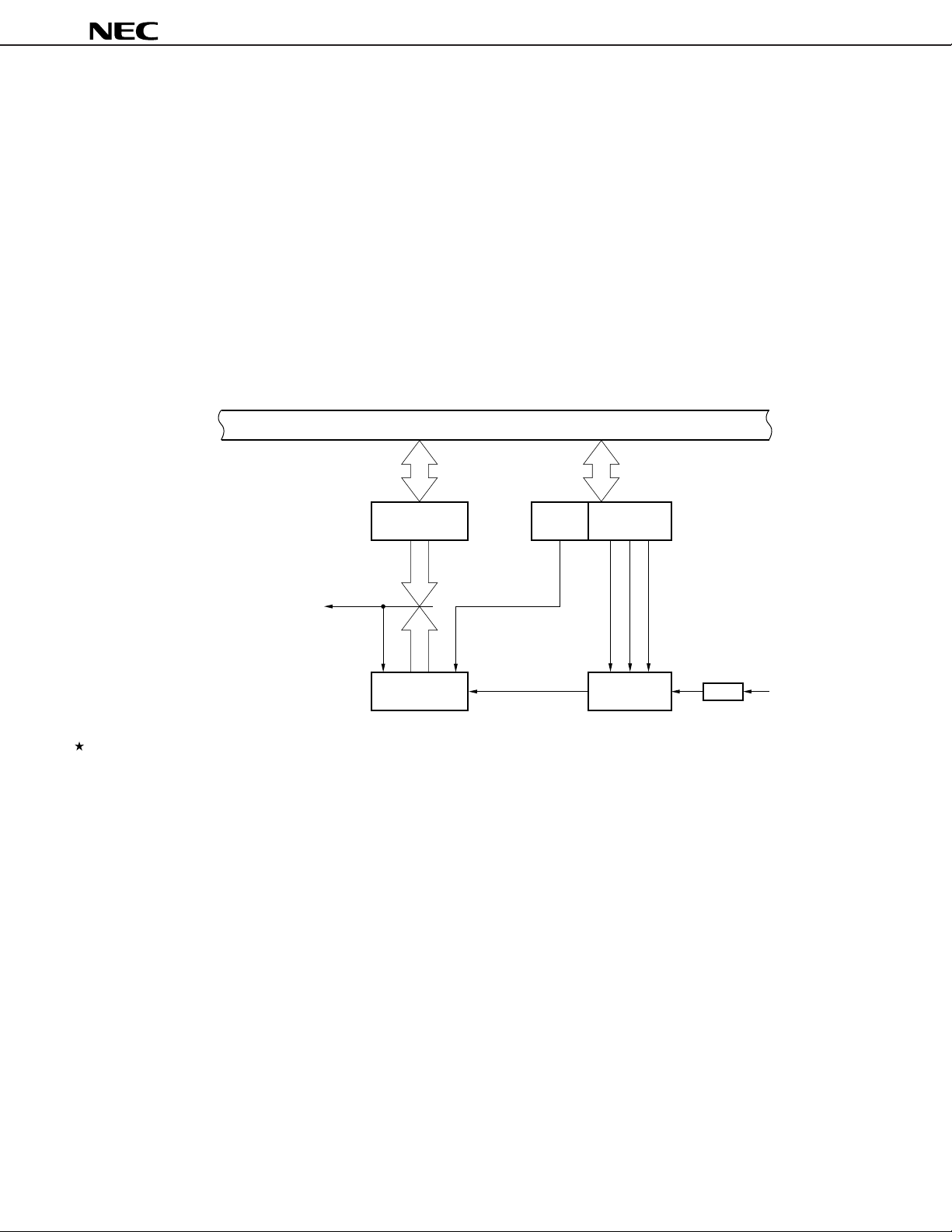
The configuration of the baud rate generator (BRG) is shown below.
Figure 9-3. Block Configuration of Baud Rate Generator (BRG)
Internal peripheral I/O bus
BRG0
Serial interface
(UART/CSI)
TMBRG0
Compare
register
Internal timer
Remarkφ = bus clock:48 M to 1.3 MHz: @input clock 6×
:36 M to 0.73 MHz: @input clock 8×
BRCE0
BPR00 to 02
Prescaler
BPRM0
1/2
φ
23Data Sheet U13675EJ2V1DS00

10. TIMER/COUNTER FUNCTION
The features of the timer/counter function are as follows:
• Measures pulse interval and frequency and outputs programmable pulse
• 16-bit measurement
• Can generate pulses of various shapes (interval pulse, one-shot pulse)
• Timer 1
• 16-bit timer/event counter
• Source of count clock: 2 types (selected by dividing system clock, external pulse input)
• Capture/compare register: × 4
• Count clear pin: TCLR
• Interrupt source: 5 types
• External pulse output: 2 pins
• Timer 4
• 16-bit interval timer
• Count clock selected by dividing system clock
• Compare register: × 1
• Interrupt source: 1 type
µ
PD705102
24
Data Sheet U13675EJ2V1DS00
 Loading...