NEC UPD705100GJ-100-8EU Datasheet

DATA SHEET
MOS INTEGRATED CIRCUIT
µ
PD705100
V830
TM
32-BIT MICROCONTROLLER
The µPD705100 (also called V830) is a microcontroller for incorporation use, which belongs to the V830 family
of the NEC original V800 seriesTM microcontrollers. The V830 can achieve high cost-performance for multimedia
equipment, by integrating quick real-time responses, high-speed arithmetic/logical instructions, and functions suitable
for individual applications.
The following user’s manual describes details of the functions of the V830. Be sure to read it before
designing an application system.
V830 User’s Manual, Hardware : U10064E
V830 User’s Manual, Architecture : U12496E
FEATURES
High-performance 32-bit architecture for
•
incorporation use • 16-bit bus system construction
• Built-in cache memory
Instruction cache : 4K bytes • Sum-of-products operation
Data cache : 4K bytes • Saturable operation
• Built-in RAM • Branch prediction
Instruction RAM : 4K bytes • Concatenation shift
Data RAM : 4K bytes • Block transfer instructions
• One-clock-pitch pipeline structure
• 16-/32-bit instructions
• Separate buses for addresses and data • 100 MHz (internal)
• 4G-byte linear addresses • 50/33 MHz (external)
• Thirty-two 32-bit general-purpose registers
• Hardware-interlocked register/flag hazard
• 16-level interrupt responses
16-bit bus fixing function
•
Instructions suitable for variable application
•
Power-saving mode
•
Maximum operating frequency
•
CMOS operation, 3.3-V operation
•
TM
ORDERING INFORMATION
Part number Package
µ
PD705100GJ-100-8EU 144-pin plastic LQFP (fine pitch) (20 × 20 mm)
The information in this document is subject to change without notice.
Document No. U11483EJ3V0DS00 (3rd edition)
Date Published January 1998 J CP(K)
Printed in Japan
The mark shows major revised points.
©
1995, 1996
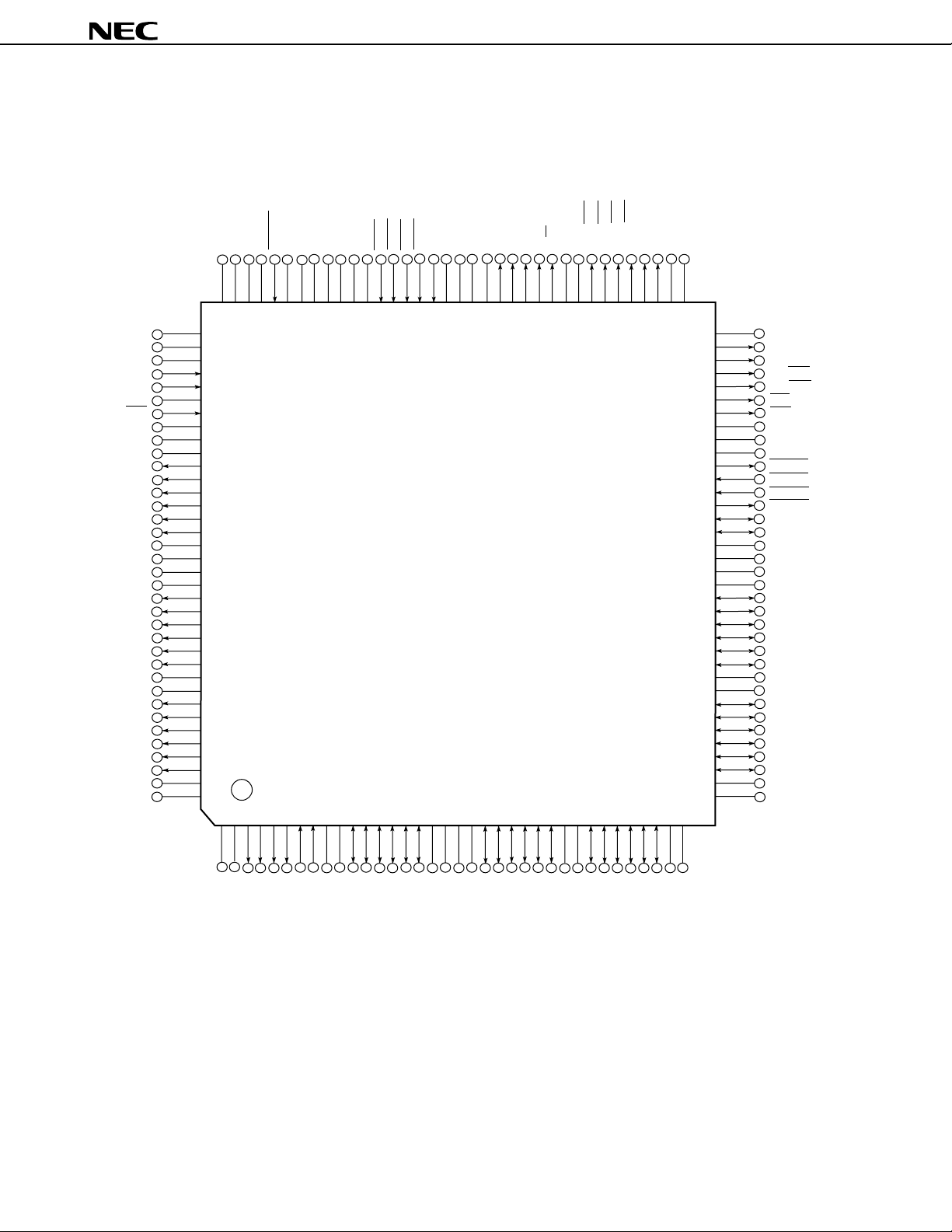
PIN CONFIGURATION
144-pin plastic LQFP (fine pitch) (20 × 20 mm)
µ
PD705100GJ-100-8EU
µ
PD705100
VDD
VDD
GND
BCLK
CMODE
IC3
NMI
V
VDD
GND
A27
A26
A25
A24
A23
A22
GND
GND
V
VDD
A21
A20
A19
A18
A17
A16
GND
V
A15
A14
A13
A12
A11
A10
V
VDD
DD
109
GND
GND
107
108
IC1
106
IC2
RESET
105
104
IC2
103
IC2
102
IC2
101
DD
V
GND
100
99
V
98
INTV3
GND
96
97
INTV1
INTV2
95
94
INTV0
93
INT
92
IC1
91
DD
GND
V
90
89
IC1
88
ST3
87
ST2
86
110
111
112
113
114
115
DD
116
117
118
119
120
121
122
123
124
125
126
DD
127
128
129
130
131
132
133
134
135
DD
136
137
138
139
140
141
142
DD
143
144
23
22
21
20
19
18
17
16
15
14
13
12
11
10
9
8
7
6
5
4
3
2
1
ST1
85
24
ST0
84
25
R/W
83
26
DD
V
82
27
A31/CS3
GND
81
80
29
28
A29/CS1
A28/CS0
A30/CS2
79
77
78
32
31
30
A5
76
33
A4
75
34
GND
74
35
36
GND
73
72
71
70
69
68
67
66
65
64
63
62
61
60
59
58
57
56
55
54
53
52
51
50
49
48
47
46
45
44
43
42
41
40
39
38
37
VDD
A3
A2
A1/BE3
BH/BE2
BE1
BE0
V
DD
VDD
GND
BCYST
READY
HLDRQ
HLDAK
D0
D16
DD
V
VDD
GND
GND
D1
D17
D2
D18
D3
D19
GND
DD
V
D4
D20
D5
D21
D6
D22
V
DD
VDD
A9A8A7
GND
GND
Caution Leave the IC1 pins open.
Connect each IC2 pin to GND via a dedicated resistor.
Connect each IC3 pin to V
2
A6
SIZ16B
DD
V
D31
D15
D30
D14
D29
GND
ASEL
DD via a dedicated resistor.
D13
GND
GND
DD
VDD
V
D28
D12
D27
D11
D26
D10
DD
V
D25D9D24D8D23
GND
D7
GND
GND

PIN NAMES
A1-A31 : Address Bus
CS0-CS3 : Chip Select
D0-D31 : Data Bus
BE0-BE3 : Byte Enable
BH : Byte or Halfword
ST0-ST3 : Status
BCYST : Bus Cycle Start
R/W : Read/Write
READY : Ready
HLDRQ : Hold Request
HLDAK : Hold Acknowledge
SIZ16B : Bus Size 16 bit
NMI : Non-Maskable Interrupt Request
INT : Interrupt Request
INTV0-INTV3 : Interrupt Level
BCLK : Bus Clock
CMODE : Clock Mode
ASEL : Address Select
RESET : Reset
DD : Power Supply
V
GND : Ground
IC1-IC3 : Internally Connected
µ
PD705100
3
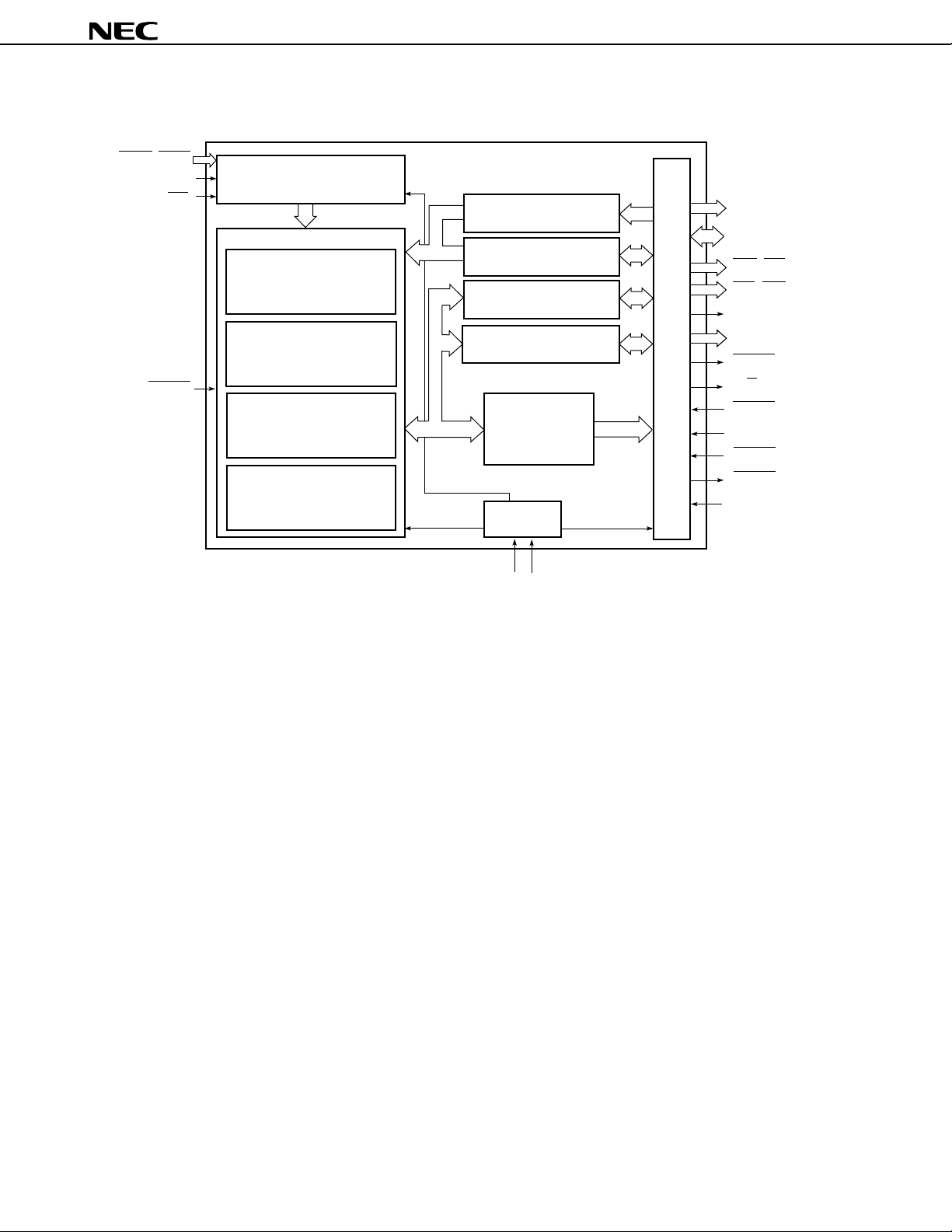
BLOCK DIAGRAM
INTV0-INTV3
INT
NMI
RESET
Interrupt controller
V830 CPU core
Barrel shifter
System registers (11)
32-bit adder
(with sum-of-products
function)
General-purpose registers
32 bits × 32
50/33 MHz
φ
= 100 MHz
Instruction cache (4K)
Instruction RAM (4K)
Data cache (4K)
Data RAM (4K)
Write buffer
(4 stages)
Clock
controller
50/33 MHz
µ
PD705100
A1-A31
D0-D31
CS0-CS3
BE0-BE3
BH
ST0-ST3
BCYST
Bus interface unit
R/W
READY
SIZ16B
HLDRQ
HLDAK
ASEL
BCLK
CMODE
4

µ
PD705100
CONTENTS
1. PIN FUNCTIONS ........................................................................................................................ 7
1.1 Pin Functions ................................................................................................................................. 7
2. ADDRESS SPACE ..................................................................................................................... 8
2.1 Memory Space ................................................................................................................................8
2.2 I/O Space ......................................................................................................................................... 10
3. 32-BIT BUS MODE..................................................................................................................... 13
3.1 Relationship between External Accesses and Byte Enable Signals ..................................... 13
4. 16-BIT BUS MODE..................................................................................................................... 14
4.1 16-Bit Bus Sizing ........................................................................................................................... 1 4
4.1.1 Byte/halfword access .................................................................................................... 14
4.1.2 Word access ................................................................................................................... 15
4.2 Relationship between External Access and Byte Enable Signals ......................................... 16
5. INTERRUPTS.............................................................................................................................. 17
5.1 Maskable Interrupts ....................................................................................................................... 17
5.2 Nonmaskable Interrupts ............................................................................................................... 18
5.3 Reset ................................................................................................................................................ 18
6. CLOCK CONTROLLER ............................................................................................................. 19
6.1 Operation Modes............................................................................................................................ 19
6.1.1 Sleep mode ..................................................................................................................... 19
6.1.2 Stop mode....................................................................................................................... 19
7. INTERNAL MEMORY................................................................................................................. 20
8. REGISTER SETS ....................................................................................................................... 21
8.1 Program Register Set .................................................................................................................... 21
8.1.1 General-purpose register set ....................................................................................... 21
8.1.2 Program counter (PC) ................................................................................................... 22
8.2 System Register Set ...................................................................................................................... 23
9. DATA SETS ................................................................................................................................24
9.1 Data Types ...................................................................................................................................... 2 4
9.1.1 Integers ........................................................................................................................... 2 5
9.1.2 Unsigned integers .......................................................................................................... 25
9.2 Data Alignment............................................................................................................................... 25
10. ADDRESS SPACE ..................................................................................................................... 26
10.1 Addressing Mode ........................................................................................................................... 27
10.1.1 Instruction addresses ................................................................................................... 27
10.1.2 Operand addresses ....................................................................................................... 28
5

µ
PD705100
11. INSTRUCTIONS ......................................................................................................................... 29
11.1 Instruction Format......................................................................................................................... 29
11.2 Instructions (Listed Alphabetically)............................................................................................ 3 1
12. INTERRUPTS AND EXCEPTIONS............................................................................................ 41
13. ELECTRICAL SPECIFICATIONS.............................................................................................. 42
14. PACKAGE DRAWING................................................................................................................ 61
15. RECOMMENDED SOLDERING CONDITIONS ........................................................................ 62
6

µ
PD705100
1. PIN FUNCTIONS
1.1 Pin Functions
Pin name Input/output Function At hold At reset
A2-A27 Tristate output Address bus Hi-Z H
A28-A31/CS0-CS3
D0-D31 Tristate input/output Bidirectional data bus Hi-Z Hi-Z
BE0, BE1 Tristate output Indicates which data bus can be used Hi-Z H
BE2/BH Indicates access to D16-D23/byte or Hi-Z H
BE3/A1 Indicates most significant byte access/A1 Hi-Z H
ST0-ST3 Indicates the status of a bus. Hi-Z 0101
BCYST Indicates the start of a bus cycle. Hi-Z H
R/W Indicates whether the bus cycle is Hi-Z H
READY Input Terminates a bus cycle. - HLDRQ Requests bus mastership. - HLDAK Output Response to HLDRQ L H
SIZ16B Input Fixes the bus width to 16 bits. - NMI Nonmaskable interrupt request - -
Note
Address bus/chip select Hi-Z/H H
for data access.
halfword access.
address.
a read or write cycle.
INT Maskable interrupt request - INTV0-INTV3 Indicates an interrupt level. - BCLK Bus clock input - CMODE Specifies the frequency ratio for the - -
external bus and the internal circuit.
ASEL Selects A28-A31/CS0-CS3. - RESET Resets the internal state. - VDD - Supplies positive power. - GND Ground potential - -
Note When used for a chip select signal, this is held at the high level.
7

µ
PD705100
2. ADDRESS SPACE
2.1 Memory Space
The V830 uses four chip select/address pins and 26 address bus pins to represent a 32-bit address. When the
chip select function is used, a 256M-byte image space is created as three spaces and a 32M-byte image space is
created as one space. When the chip select function is not used, a 4G-byte linear address space is created.
Area 40000000H-7FFFFFFFH in the memory space is reserved as an uncachable area. When this area is
accessed, the cache function is not effective. For all other areas, the cache function is effective.
Within the memory space, built-in instruction RAM and built-in data RAM are mapped. By accessing these areas,
an instruction can be fetched and data loaded/stored within one cycle (internal clock) without activating a bus cycle
externally. Data in the built-in instruction RAM, however, cannot be accessed by using the load/store instructions. Nor
can instructions be fetched from the built-in data RAM. These built-in RAMs are mapped to the cachable area; however,
they are not cached.
8
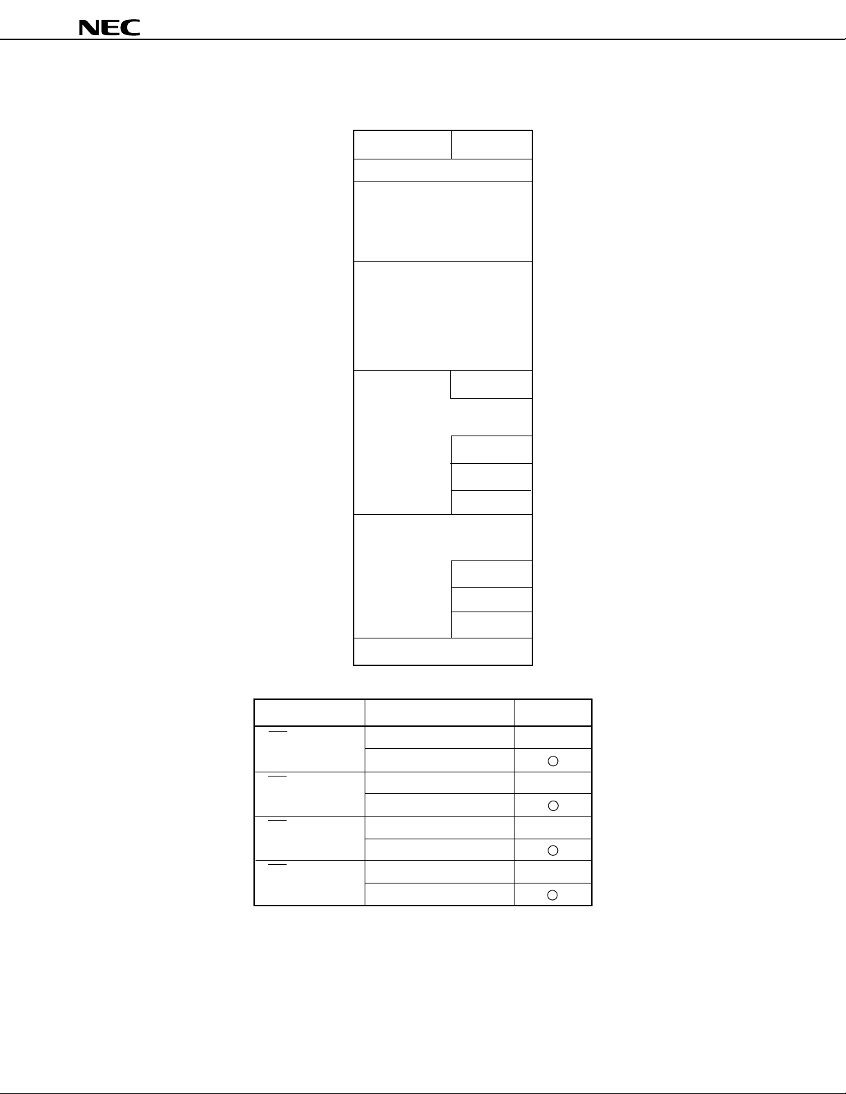
Figure 2-1. Memory Map
µ
PD705100
FFFFFFFFH
C0000000H
BFFFFFFFH
80000000H
7FFFFFFFH
40000000H
3FFFFFFFH
CS0
Built-in instruction RAM
Cachable area
Cachable area
CS0
Uncachable area
CS3
CS2
CS1
Cachable area
FFFFFFFFH
FE001000H
FE000FFFH
FE000000H
7FFFFFFFH
7E000000H
6FFFFFFFH
60000000H
5FFFFFFFH
50000000H
4FFFFFFFH
40000000H
00000000H
Chip select signal
CS0
CS1
CS2
CS3
CS3
CS2
CS1
Built-in data RAM
7E000000H-7FFFFFFFH
FE001000H-FFFFFFFFH
40000000H-4FFFFFFFH
00001000H-0FFFFFFFH
50000000H-5FFFFFFFH
10000000H-1FFFFFFFH
60000000H-6FFFFFFFH
20000000H-2FFFFFFFH
2FFFFFFFH
20000000H
1FFFFFFFH
10000000H
0FFFFFFFH
00001000H
00000FFFH
00000000H
Cachable Address space
×
×
×
×
9

µ
PD705100
2.2 I/O Space
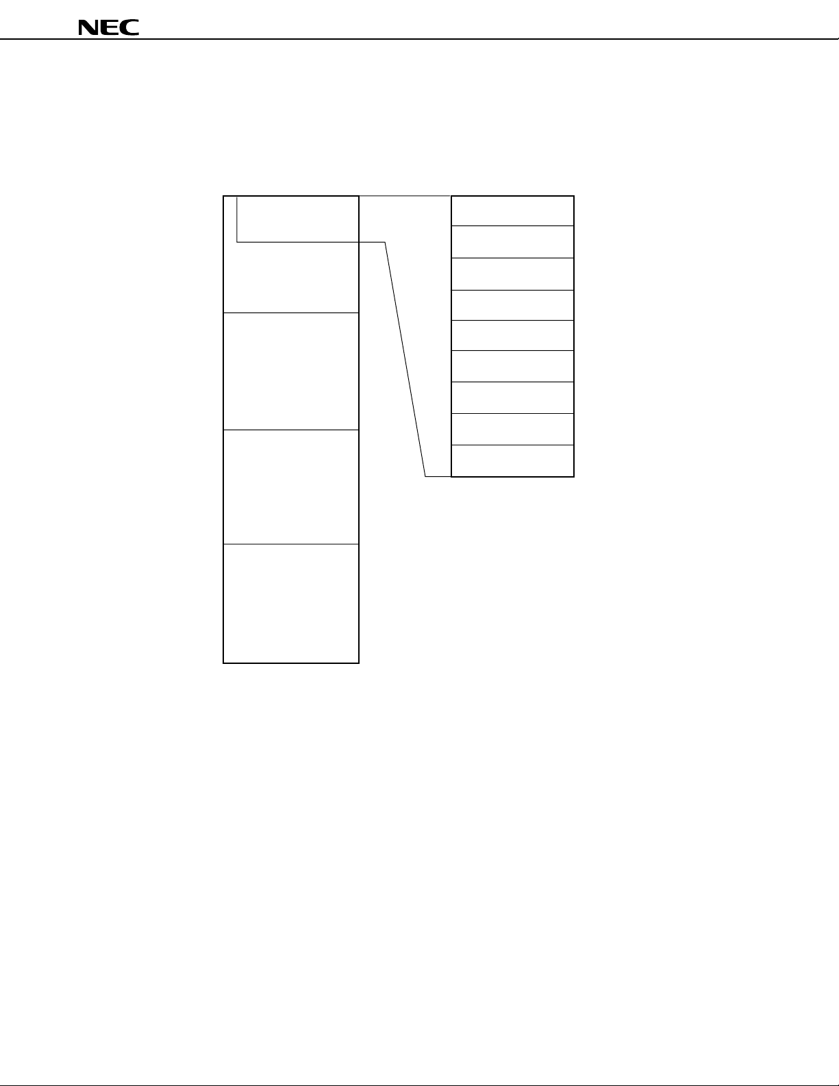
The V830 represents the I/O space using 32 bits and supports a linear address space of up to 4G bytes.
The 1G-byte area C0000000H-FFFFFFFFH is reserved as an internal I/O area. External I/O cannot be placed in
this area. When accessing that part of the internal I/O area to which internal I/O is not allocated, normal operation
cannot be guaranteed.
Figure 2-2. I/O Map
FFFFFFFFH
Internal I/O area
(1G byte)
C0000000H
BFFFFFFFH
External I/O area
(1G byte)
80000000H
7FFFFFFFH
40000000H
3FFFFFFFH
00000000H
External I/O area
(1G byte)
External I/O area
(1G byte)
10

µ
PD705100
The cache function is not effective within the I/O space. When the chip select function is used, the area is used
as the 256M-byte image space represented by A2-A27.
Figure 2-3. Image Space Used When Chip Select Function is Used
FFFFFFFFH
Internal I/O area
C0000000H
BFFFFFFFH
Image 11
Image 10
Image 9
80000000H
7FFFFFFFH
40000000H
3FFFFFFFH
00000000H
Image 8
Image 7
Image 6
Image 5
Image 4
Image 3
Image 2
Image 1
Image 0
11
µ
PD705100
The upper 1G-byte area (C0000000H-FFFFFFFFH) in the I/O space is reserved for internal I/O. To access internal
I/O, the IN.W/OUT.W instructions (in words) must be used. When the internal I/O area is accessed, an external bus
cycle is not activated.
Figure 2-4. Internal I/O Area
FFFFFFFFH
C0000000H
BFFFFFFFH
80000000H
7FFFFFFFH
40000000H
3FFFFFFFH
Built-in periphery
Internal I/O area
(1G byte)
External I/O area
(1G byte)
External I/O area
(1G byte)
External I/O area
(1G byte)
Reserved
PLLCR
CMCR
Reserved
IRAMR
Reserved
ICTR
Reserved
DCTR
FFFFFFFFH
FFFFFFFCH
FFFFFFFBH
FFFFFFF8H
FFFFFFF7H
FFFFFFF4H
FFFFFFF3H
FE001000H
FE000FFFH
FE000000H
FDFFFFFFH
FA001000H
FA000FFFH
FA000000H
F9FFFFFFH
F2001000H
F2000FFFH
F2000000H
12
00000000H

µ
PD705100
3. 32-BIT BUS MODE
If the SIZ16B input, sampled at reset, is inactive, the external bus width becomes 32 bits (32-bit bus mode). In
this mode, BE2/BH acts as BE2 and BE3/A1 acts as BE3.
3.1 Relationship between External Accesses and Byte Enable Signals
In 32-bit bus mode, BE0-BE3 are output. External accesses are related to byte enable signals as indicated below.
Table 3-1. 32-Bit Bus Mode
Data length Operand address Byte enable State
Bit 1 Bit 0 BE3 BE2 BE1 BE0
Byte 0 0 1 1 1 0 Ta,Ts
0 1 1 1 0 1 Ta,Ts
1 0 1 0 1 1 Ta,Ts
1 1 0 1 1 1 Ta,Ts
Halfword 0 0 1 1 0 0 Ta,Ts
1 0 0 0 1 1 Ta,Ts
Word 0 0 0 0 0 0 Ta,Ts
Burst transfer 0 0 0 0 0 0 Ta,Tb1
000000Tb2
000000Tb3
000000Tb4
13
µ
PD705100
4. 16-BIT BUS MODE
If the SIZ16B input, sampled at reset, is active, the external bus width becomes 16 bits (16-bit bus mode). In this
mode, the low-order 16 bits (D0-D15) of the data bus are valid, BE2/BH acts as BH and BE3/A1 acts as A1. The highorder 16 bits (D16-D31) of the data bus enter the high-impedance state.
4.1 16-Bit Bus Sizing
The V830 has a bus sizing function by which, to enable access from the data bus to 16 bits of memory or the
I/O space, data can be transferred using only the low-order 16 bits of the 32-bit data bus.
When the SIZ16B input is activated upon a reset, the external data bus width becomes 16 bits (16-bit bus mode).
In 16-bit bus mode, D16-D31 are all set to the high-impedance state and BE0, BE1, BH, and A1 are output in a way
suited to a 16-bit bus system. Connection to D16-D31 is not necessary. The SIZ16B input can be changed only when
the V830 is reset. It cannot be changed at any other time.
4.1.1 Byte/halfword access
Bus cycles in either of two bus states (Ta and Ts) are used for byte/halfword access.
(1) Upper halfword
During read cycles, data is read from D0-D15.
During write cycles, D16-D31 data read from the write buffer is output to D0-D15.
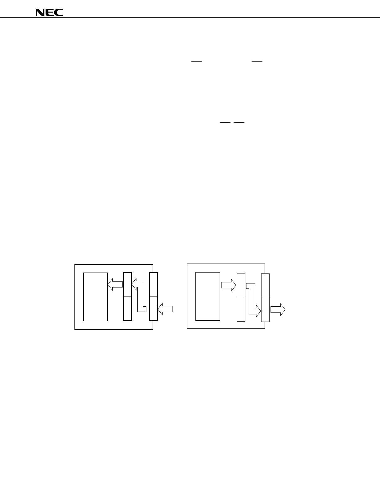
Figure 4-1 illustrates the operation for upper halfword access. In this figure, B indicates the upper halfword (highorder 16 bits of the word).
Read cycle
Internal
operation
unit
Figure 4-1. Upper Halfword Access
Read buffer
31
B
16
15
0
Data bus
31
16
15
B
0
Write cycle
Internal
operation
unit
Write buffer
31
B
16
15
0
Data bus
31
16
15
B
0
14
µ
PD705100
(2) Lower halfword
During read cycles, data is read from D0-D15.
During write cycles, D0-D15 data read from the write buffer is output to D0-D15.
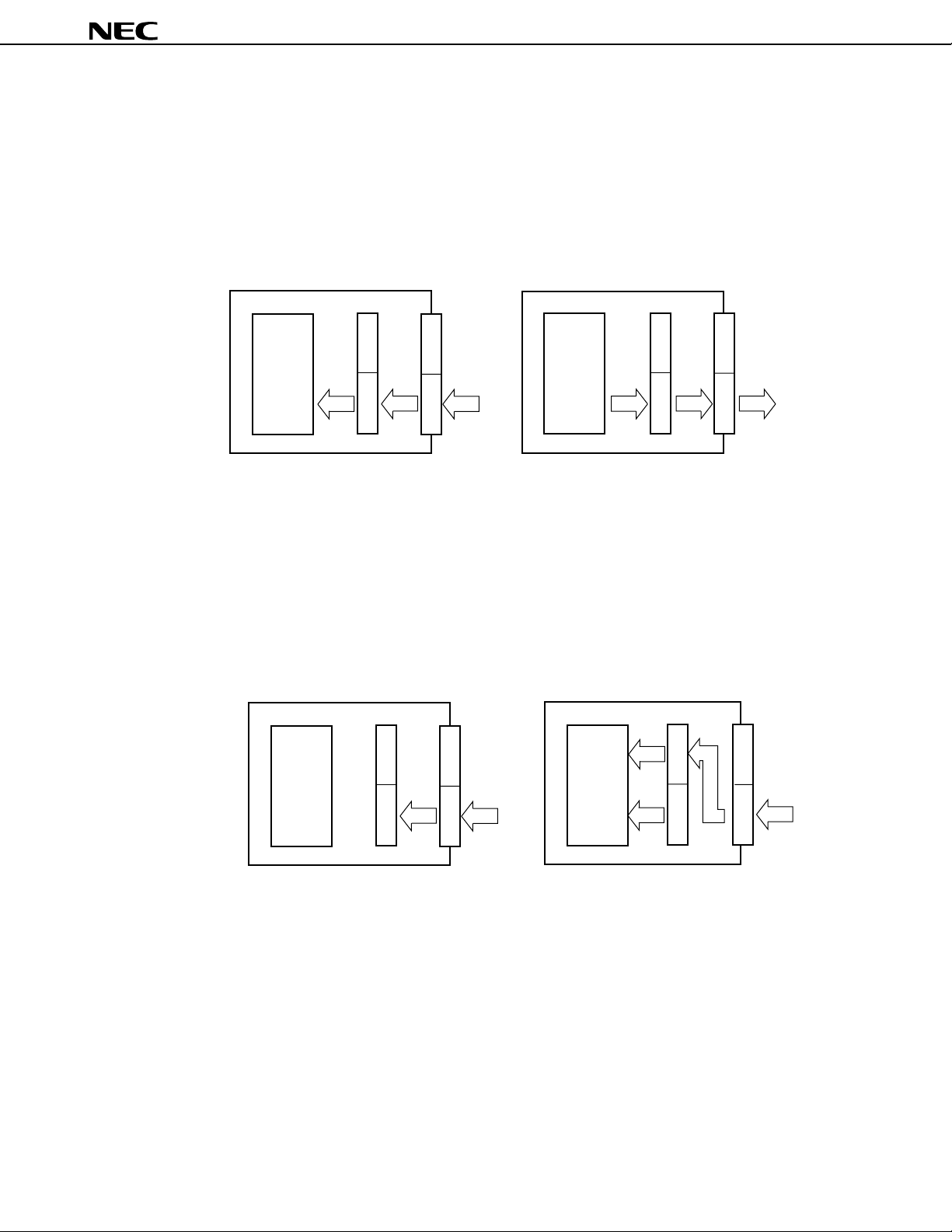
Figure 4-2 shows the operation for lower halfword access. In this figure, A indicates the lower halfword (low-order
16 bits of the word).
Figure 4-2. Lower Halfword Access
Read cycle Write cycle
Read buffer
31
31
Data bus
Write buffer
31
Data bus
31
Internal
operation
unit
16
15
16
15
A
0
A
0
Internal
operation
unit
16
15
16
15
A
0
A
0
4.1.2 Word access
Bus cycles in any of three bus states (Ta, Tw1, and Tw2) are used for word access.
During a read cycle, the low-order 16 bits of data and high-order 16 bits of data are sampled from D0-D15 in the
Tw1 and Tw2 state, respectively. During write cycles, the low-order 16 bits of data and high-order 16 bits of data are
output to D0-D15 in the Ta/Tw1 state and Tw2 states, respectively.
Figure 4-3. Read Cycle
Internal
operation
unit
Tw1 state
Read buffer
31
16
15
0
Data bus
31
16
15
A
A
0
Tw2 state
Internal
operation
unit
Read buffer
31
B
16
15
A
0
Data bus
31
16
15
B
0
15
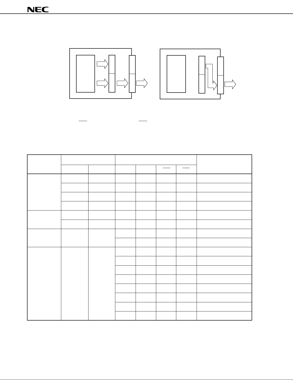
Figure 4-4. Write Cycle
µ
PD705100
Ta, Tw1 state
Internal
operation
unit
Write buffer
31 31
B
16
15
A
0
Data bus
16
15
A
0
Internal
operation
unit
Tw2 state
Write buffer
31
16
15
0
Data bus
31
B
16
15
B
0
4.2 Relationship between External Access and Byte Enable Signals
In 16-bit bus mode, the BE3/A1 output acts as A1 and BE2/BH output acts as BH. External accesses are related
to the byte enable signals as indicated below.
Table 4-1. 16-Bit Bus Mode
Data length Operand address Byte enable State
Bit 1 Bit 0 A1 BH BE1 BE0
Byte 0 0 0 1 1 0 Ta,Ts
0 1 0 1 0 1 Ta,Ts
1 0 1 1 1 0 Ta,Ts
1 1 1 1 0 1 Ta,Ts
Halfword 0 0 0 1 0 0 Ta,Ts
1 0 1 1 0 0 Ta,Ts
Word 0 0 0 0 0 0 Ta,Tw1
1 0 0 0 Tw2
Burst transfer 0 0 0 0 0 0 Ta,Tb1
1 0 0 0 Tb2
0 0 0 0 Tb3
1 0 0 0 Tb4
0 0 0 0 Tb5
1 0 0 0 Tb6
0 0 0 0 Tb7
1 0 0 0 Tb8
16

µ
PD705100
5. INTERRUPTS
V830 interrupts include maskable interrupts, nonmaskable interrupts, and reset operations.
5.1 Maskable Interrupts
Maskable interrupt requests are themselves denoted by INT, and their interrupt levels by INTV0 to INTV3.
The following lists pin states and the corresponding interrupt levels.
Table 5-1. Interrupt Levels
Interrupt level INTV3 INTV2 INTV1 INTV0
15 0000
14 0001
13 0010
12 0011
11 0100
10 0101
90110
80111
71000
61001
51010
41011
31100
21101
11110
01111
INT and INTV0 to INTV3 are level inputs. The V830 samples an INT at the rising edge of a bus clock
pulse. INT and INTV0 to INTV3 should be held at the active level until the V830 accepts the interrupt request and
posts to a peripheral, by software, notification of the acceptance of the interrupt request. Although a change to a higher
interrupt level is possible, the timing at which an interrupt request is detected cannot then be posted to peripheral.
Hence, an interrupt request made before such a change may be accepted. If the interrupt request input (INT, INTV0INTV3) fails to satisfy the setup time requirement for the bus clock pulse, the interrupt request will be detected at the
rising edge of the next bus clock pulse.
Upon accepting an interrupt request, the V830 jumps to a fixed address to start interrupt handling. The target
address of the jump is set to FE0000n0H (built-in RAM) or FFFFFEn0H (external memory), where n is the interrupt
level, either of which may be specified with the IHA bit of the system register, HCCW.
Caution Interrupt level 15 is reserved for use by development tools (in-circuit emulator, ROM emulator,
etc). If the user uses interrupt level 15, those development tools may fail to operate.
17

µ
PD705100
5.2 Nonmaskable Interrupts
The V830 samples an NMI at the rising edge of a bus clock pulse. When the NMI changes from the high to low
level, an interrupt request is detected. Once a nonmaskable interrupt request has been detected, the NMI can
subsequently be deactivated at any time because the NMI is detected at the falling edge. An interrupt request thus
detected is retained in the CPU until the CPU starts interrupt handling.
Upon accepting a nonmaskable interrupt, the V830 jumps to the fixed address (FFFFFFD0H). If another
nonmaskable interrupt is issued during nonmaskable interrupt handling (the NP bit of PSW is set to1), it is retained
in the processor. If, however, another nonmaskable interrupt request is issued during clearing of the latch circuit by
internal processing after the start of nonmaskable interrupt handling, it is not retained in the processor.
5.3 Reset
The V830 can be reset by inputting a low-level signal of 20 or more clock pulses to RESET. After the V830 has
been reset, the CPU starts program execution from address FFFFFFF0H.
If RESET is driven high, the CPU starts instruction fetching from the reset address.
Immediately after power-on or in the stop-mode state, the active pulse width of the RESET should be determined
by adding the PLL oscillation settling time to the active level of 20 clock pulses.
18

µ
PD705100
6. CLOCK CONTROLLER
6.1 Operation Modes
The V830 supports two clock stop functions, namely, sleep mode and stop mode. Transition from one mode to
another is made by executing special instructions HALT or STBY. The following lists the features of these modes:
Table 6-1. Operation Modes
Sleep mode Stop mode
V830 Internal state Internal clock stop Internal clock stop
PLL operation continuous PLL operation stop
Bus hold acceptable Bus hold unacceptable
Built-in RAM/cache data hold Built-in RAM/cache data hold
Entry to mode HALT instruction STBY instruction
Escape from mode Maskable interrupt/NMI/reset NMI/reset
6.1.1 Sleep mode
The V830 enters sleep mode upon the execution of a HALT instruction. On the other hand, escape from sleep
mode can be realized by a maskable interrupt, NMI, or reset operation.
In sleep mode, bus hold requests can be accepted. During bus hold, the status becomes high impedance and no
halt acknowledge status is output. At the end of bus hold, a halt acknowledge status is output in sync with the rising
edge of a bus clock pulse.
6.1.2 Stop mode
The V830 enters stop mode when an STBY instruction is executed. On the other hand, escape from stop mode
can be realized using an NMI or a reset operation. The power consumption in stop mode is less than that in the sleep
mode because the PLL circuit stops.
Also, no bus hold requests are accepted in the stop mode.
19
µ
PD705100
7. INTERNAL MEMORY
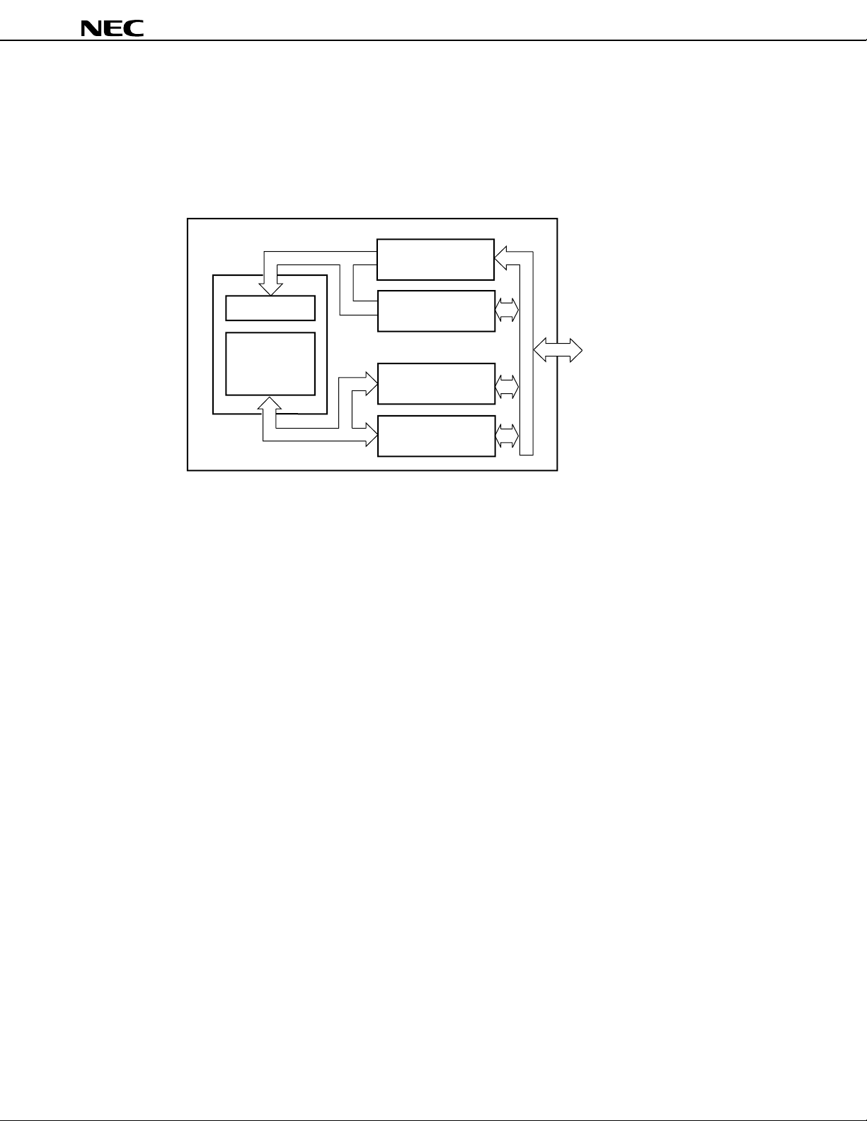
The V830 has a 4K bytes × 4 internal memory, consisting of four blocks (instruction cache, data cache, instruction
RAM, and data RAM). The V830 allows any of these internal memory blocks to be accessed in one cycle.
Figure 7-1. Built-In Cache Configuration
Instruction bus
V830 CPU
core
Instruction cache
Decoder
Execution unit
Data bus
Cautions 1. Data can not be written into the instruction cache or instruction RAM.
2. A instruction can not be written into the data cache or data RAM.
Instruction RAM
External memory
Data cache
Data RAM
20
 Loading...