NEC UPD70433R-12, UPD70433R-16, UPD70433GJ-16-3EB, UPD70433GJ-12-3EB, UPD70433GD-16-5BB Datasheet
...
DATA SHEET
MOS INTEGRATED CIRCUIT
µ
PD70433
V55PI
TM
16-BIT MICROPROCESSOR
DESCRIPTION
The µPD70433 (V55PI) is a microprocessor in which a 16-bit CPU, RAM, serial interface, parallel interface, A/D
converter, timers, DMA controller, interrupt controller, etc., are integrated in a single chip.
The V55PI is software-compatible with the µPD70320 and 70330 (V25TM and V35TM) single-chip microcontrollers. The
V55PI provides a migration path from the V25. It offers higher-level functions and higher performance, and is particularly
suitable for control of data processing systems associated with mechanical control, including printer and facsimile.
Detailed functions are described in the following user’s manuals, which should be read when carrying out
design work.
• V55PI User’s Manual Hardware : U10514E
• V55PI User’s Manual Instruction : U10231E
FEATURES
• Internal 16-bit architecture, selectable external data bus width (16/8 bits)
TM
• Software compatible with V20
• Minimum instruction cycle: 160 ns/12.5 MHz (external 25 MHz)
• Address space: 16M bytes: 1-Mbyte basic memory space
• Register file space (in on-chip RAM) : 512 bytes/16 register banks
• I/O space : 64K bytes
• Automatic wait control with memory space divided in variable sizes (max. 6 blocks)
• I/O line (input ports: 11 bits, input/output ports: 42 bits)
• DMA controller (DMAC): Max. 4-channel configuration possible
• Four DMA transfer modes (single transfer, demand release, single step, burst)
• Intelligent DMA modes 1 and 2
• Serial interface: 2 channels
• Asynchronous mode (UART) or clocked mode (CSI) selectable
• Parallel interface: 8 bits
• Centronics data input/output and general-purpose data input/output
• A/D converter (8 bits): 4 channels
• Real-time output port: 4 bits × 2 channels or 8 bits × 1 channel
• PMW (Pulse Width Modulation) output function : 8 bits
and V30TM (native mode) and V25 and V35 (includes additional instructions)
125 ns/16 MHz (external 32 MHz)
16-Mbyte extended memory space
Document No. U11775EJ4V0DS00 (4th edition)
Previous No. IC-8257
Date Published November 1996 P
Printed in Japan
The information in this document is subject to change without notice.
The mark shows major revised points.
©
1995

• Interrupt controller
• Programmable priority (4 levels)
• Three interrupt servicing methods
Vectored interrupt function, register bank switching function, macro service function
• 16-bit timer: 4 channels
• Watchdog timer function
• Software interval timer (16 bits)
• Address field wait insertion function and RAS/CAS switchover timing generation function
• DRAM and pseudo-SRAM refresh functions
• Standby functions (STOP mode, HALT mode)
• On-chip clock generator
APPLICATIONS
• Control of data processing systems using serial or parallel communication
(Data processing terminals, printer, G3 facsimile, etc.)
ORDERING INFORMATION
µ
PD70433
Part Number Package
µ
PD70433GD-12-5BB 120-pin plastic QFP (28 × 28 mm) 12.5
µ
PD70433GD-16-5BB 120-pin plastic QFP (28 × 28 mm) 16
µ
PD70433R-12 132-pin ceramic PGA 12.5
µ
PD70433R-16 132-pin ceramic PGA 16
µ
PD70433GJ-12-3EB 120-pin plastic QFP (fine pitch) (20 × 20 mm) 12.5
µ
PD70433GJ-16-3EB 120-pin plastic QFP (fine pitch) (20 × 20 mm) 16
Maximum Operating
Frequency (MHz)
2
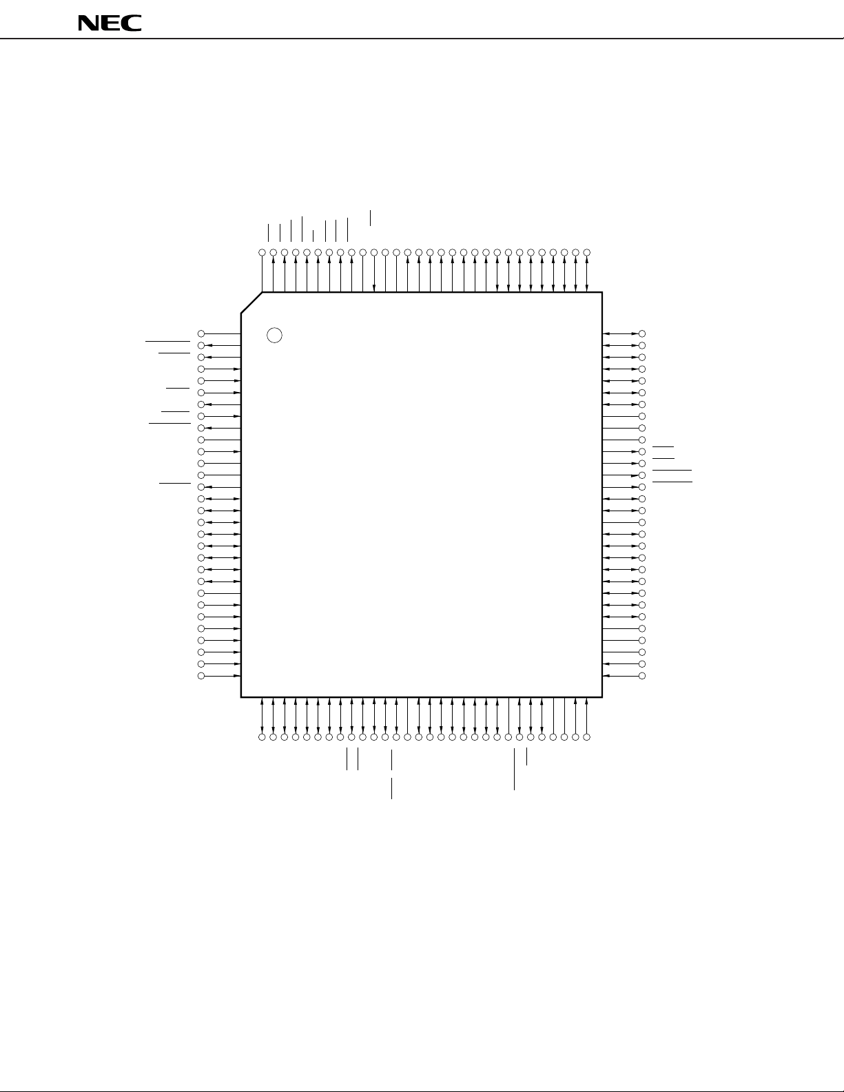
PIN CONFIGURATION (TOP VIEW)
(1) 120-Pin Plastic QFP (28 × 28 mm), 120-pin plastic QFP (fine pitch) (20 × 20 mm)
µ
PD70433GD-xx-5BB
µ
PD70433GJ-xx-3EB
OPEN
DEX
RAS
IORD
IOWRRDWRL
WRH
ASTB
IC (L)
D8/D16
GND
VDDA23
A22
A21
A20
A19
A18
A17
A16
AD15
AD14
AD13
AD12
AD11
AD10
AD9
AD8
AD7
µ
PD70433
V
BUSLOCK
HLDAK
HLDRQ
READY
POLL
CLKOUT
RESET
WDTOUT
V
X1
X2
GND
REFRQ
P00
P01
P02
P03
P04
P05
P06
P07
GND
P10/NMI
P11/INTP0
P12/INTP1
P13/INTP2
P14/INTP3/TI
P15/INTP4
P16/INTP5
119
117
115
113
111
109
107
105
103
120
118
116
114
112
110
108
106
DD
DD
1
2
3
4
5
6
7
8
9
10
11
12
13
14
15
16
17
18
19
20
21
22
23
24
25
26
27
28
29
30
313233343536373839404142434445464748495051525354555657585960
104
101
102
1009998979695949392
91
90
89
88
87
86
85
84
83
82
81
80
79
78
77
76
75
74
73
72
71
70
69
68
67
66
65
64
63
62
61
AD6
AD5
AD4
AD3
AD2
AD1
AD0
IC (H)
GND
V
DD
TCE1
TCE0
DMAAK1
DMAAK0
P81/DMARQ1
P80/DMARQ0
V
DD
P77/RTPT7
P76/RTPT6
P75/RTPT5
P74/RTPT4
P73/RTPT3
P72/RTPT2
P71/RTPT1
P70/RTPT0
GND
AV
DD
AV
REF
P63/ANI3
P62/ANI2
SS
DD
V
AV
P51/ACK
P52/BUSY
P50/DATASTB
P60/ANI0
P61/ANI1
P20/PWM
P21/TO00
P22/TO01
P23/TO20
P24/TO21
P25/TO30
C/SCK0
X
P33/CTS0
D0/SB1/SI0
X
D0/SB0/SO0
X
P32/T
P31/R
P30/T
DD
V
D1/SI1
X
D1/SO1
X
P35/R
P34/T
P36/SCK1/CTS1
P40/PD0
P41/PD1
P42/PD2
P43/PD3
P44/PD4
P45/PD5
GND
P46/PD6
P47/PD7
Remark IC: Internally Connected
Notes 1. The IC (H) pin should be connected to VDD with an external resistor (1 to 10 kΩ).
2. The IC (L) pin should be connected to GND with an external resistor (1 to 10 k
Ω).
3. No connection should be made to the OPEN pin.
3
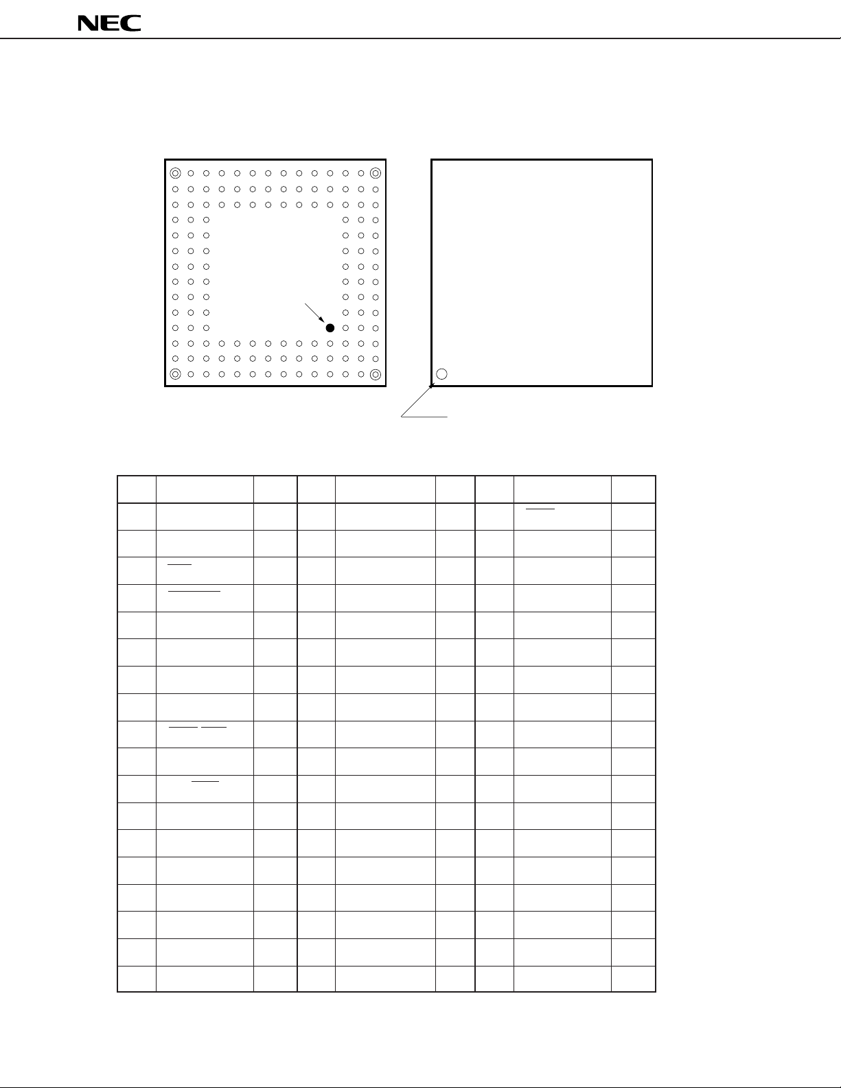
(2) 132-Pin Ceramic PGA
µ
PD70433R-xx
Bottom View
Locator Pin
µ
PD70433
Top View
14
13
12
11
10
9
8
7
6
5
4
3
2
1
ABCDEFGHJKLMNP
Index Mark
PNMLKJHGFEDCBA
Remark The locator pin is not included in the pin count.
No. Signal Nane Port No. Signal Name Port No. Signal Name Port
A1 ANI1 P61 B5 PD7 P47 C9 CTS0 P33
A2 AVSS –– B6 PD5 P45 C10 TO30 P25
A3 ACK P51 B7 PD2 P42 C11 TO00 P21
A4 DATASTB P50 B8 PD0 P40 C12 NC ––
A5 PD6 P46 B9 RXD1/SI1 P35 C13 INTP4 P15
A6 PD4 P44 B10 RXD0/SB1/SI0 P31 C14 INTP0 P11
A7 PD1 P41 B11 TO21 P24 D1 RTPT2 P72
A8 NC –– B12 TO01 P22 D2 GND ––
A9 SCK1/CTS1 P36 B13 NC –– D3 ANI3 P63
A10 TXD1/SO1 P34 B14 INTP3/TI P14 D12 INTP5 P16
A11 TXC/SCK0 P32 C1 RTPT1 P71 D13 INTP2 P13
A12 TXD0/SB0/SO0 P30 C2 AVREF –– D14 NMI P10
A13 TO20 P23 C3 NC –– E1 RTPT5 P75
A14 PWM P20 C4 NC –– E2 RTPT3 P73
B1 AVDD –– C5 VDD –– E3 RTPT0 P70
B2 ANI2 P62 C6 GND –– E12 INTP1 P12
B3 ANI0 P60 C7 PD3 P43 E13 GND ––
B4 BUSY P52 C8 VDD –– E14 –– P06
4

No. Signal Nane Port No. Signal Name Port No. Signal Name Port
F1 RTPT7 P77 K3 AD2 ––– N3 AD9 –––
F2 RTPT6 P76 K12 POLL ––– N4 AD11 –––
F3 RTPT4 P74 K13 WDTOUT ––– N5 AD14 –––
F12 ––– P07 K14 X1 ––– N6 A18 –––
F13 ––– P05 L1 AD0 ––– N7 A21 –––
F14 ––– P04 L2 AD3 ––– N8 A23 –––
G1 NC ––– L3 AD6 ––– N9 D8/D16 –––
G2 DMARQ0 P80 L12 BUSLOCK ––– N10 ASTB –––
G3 VDD ––– L13 READY ––– N11 IOWR –––
G12 ––– P03 L14 RESET ––– N12 DEX –––
G13 ––– P02 M1 AD1 ––– N13 VDD –––
G14 ––– P01 M2 AD5 ––– N14 HLDRQ –––
µ
PD70433
H1 DMARQ1 P81 M3 NC ––– P1 AD7 –––
H2 DMAAK0 ––– M4 AD8 ––– P2 AD10 –––
H3 DMAAK1 ––– M5 AD12 ––– P3 AD13 –––
H12 REFRQ ––– M6 A16 ––– P4 AD15 –––
H13 ––– P00 M7 A20 ––– P5 A17 –––
H14 NC ––– M8 V DD ––– P6 A19 –––
J1 TCE0 ––– M9 WRH ––– P7 NC –––
J2 TCE1 ––– M10 IORD ––– P8 A22 –––
J3 GND ––– M11 NC ––– P9 GND –––
J12 VDD ––– M12 NC ––– P10 IC (L) –––
J13 X2 ––– M13 HLDAK ––– P11 WRL –––
J14 GND ––– M14 CLKOUT ––– P12 RD –––
K1 VDD ––– N1 AD4 ––– P13 RAS –––
K2 IC (H) ––– N2 NC ––– P14 OPEN –––
Remark IC: Internally Connected
NC: Non-Connection
Notes 1. The IC (H) pin should be connected to V
2. The IC (L) pin should be connected to GND with an external resistor (1 to 10 k
3. No connection should be made to the OPEN pin.
DD with an external resistor (1 to 10 kΩ).
Ω).
5
6
T
R
X
D0/SB0/SO0
V
DD
GND
GENERAL
REGISTERS
&
DATA MEMORY
512 BYTES
ALU
EXU
X
D0/SB1/SI0
T
X
C/SCK0
CTS0
R
X
D1/SI1
CTS1/SCK1
T
X
D1/SO1
PD0–PD7
DATASTB
8
ACK
BUSY
ANI0–ANI3
AV
AV
DD
SS
4
AV
REF
X2
X1
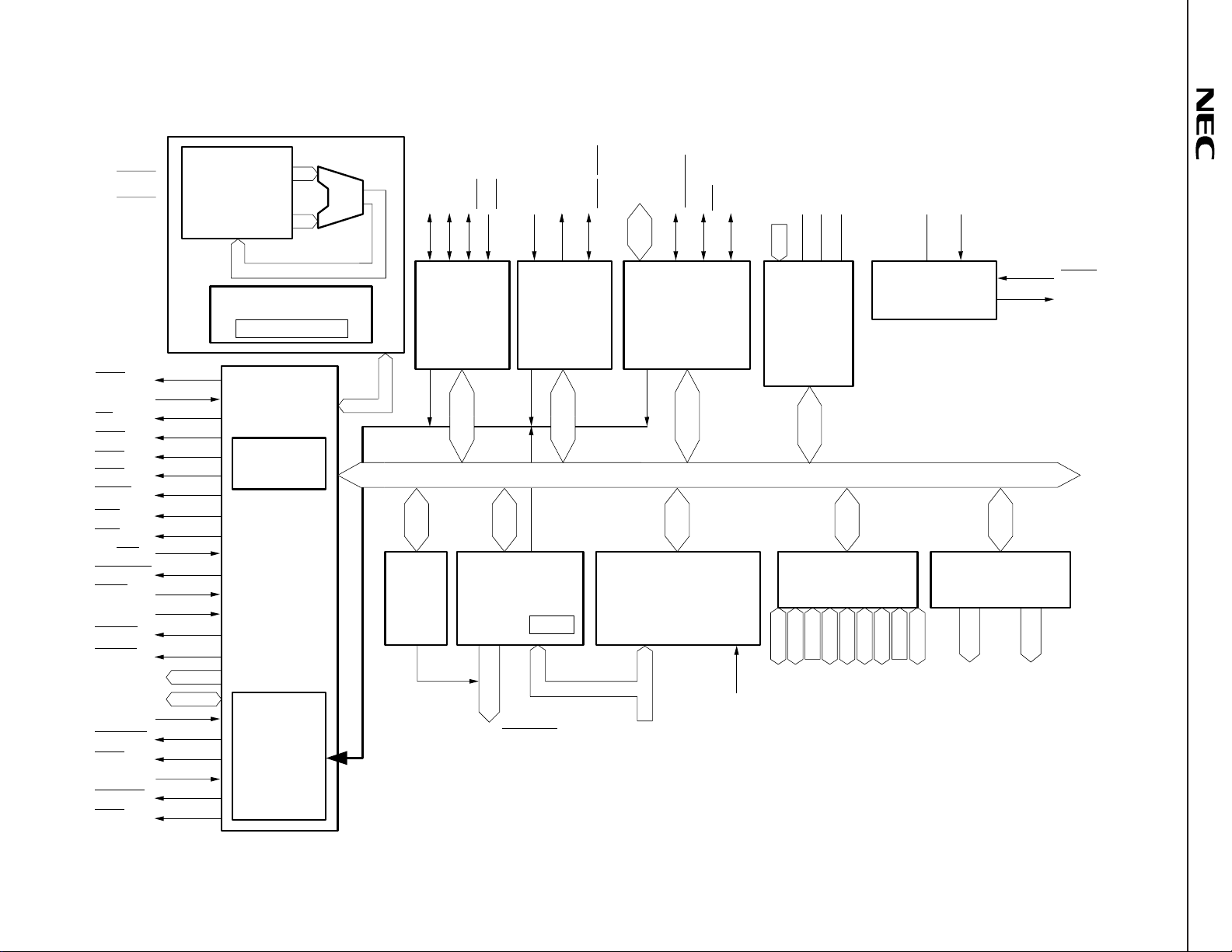
INTERNAL BLOCK DIAGRAM
ASTB
READY
RD
WRH
WRL
IORD
IOWR
RAS
DEX
D8/D16
BUSLOCK
POLL
HLDRQ
HLDAK
REFRQ
A16–A23
AD0–AD15
DMARQ0
DMAAK0
TCE0
DMARQ1
DMAAK1
TCE1
MICRO SEQUENCE
CONTROL
MICRO ROM
BCU
PREFETCH
QUEUE
6 BYTES
BUS
CONTROL
&
PREFETCH
CONTROL
DMAC
DMA
request
PWM
UNIT
• PWM
• TO00
• TO20
• TO03
TIMER/
COUNTER
UNIT
WDT
• WDTOUT
• TO01
• TO21
PIUUART/CSIUART/CSI
PROGRAMMABLE
INTERRUPT
CONTROLLER
64
• INTP0
• INTP1
• INTP2
• INTP3/TI
• INTP4
• INTP5
NMI
8-BIT
A/D
PORT7
PORT8
SYSTEM
CONTROL
PORT RTOP
PORT0
PORT1
PORT2
PORT3
PORT4
PORT5
PORT6
RTP4–RTP7
RESET
CLKOUT
44876783482
RTP0–RTP3
µ
PD70433

µ
PD70433
CONTENTS
1. PIN FUNCTIONS ....................................................................................................................................... 1 0
1.1 LIST OF PIN FUNCTION .................................................................................................................................... 10
1.1.1 Port Pins ................................................................................................................................................ 10
1.1.2 Non-Port Pins........................................................................................................................................11
2. BLOCK CONFIGURATION....................................................................................................................... 14
2.1 BUS CONTROL UNIT (BCU) ............................................................................................................................. 14
2.2 EXECUTION UNIT (EXU)...................................................................................................................................14
2.3 INTERRUPT CONTROLLER (INTC) .................................................................................................................1 4
2.4 DMA CONTROLLER (DMAC) ........................................................................................................................... 14
2.5 UART/CLOCKED SERIAL INTERFACE (UART/CSI)......................................................................................1 4
2.6 PARALLEL INTERFACE UNIT (PIU)................................................................................................................14
2.7 A/D CONVERTER UNIT (8-BIT A/D) ................................................................................................................ 14
2.8 TIMER/COUNTER UNIT (TCU) .........................................................................................................................14
2.9 PWM (PULSE WIDTH MODULATION) UNIT (PWM).......................................................................................14
2.10 WATCHDOG TIMER (WDT) ..............................................................................................................................14
2.11 PORTS (PORT)................................................................................................................................................... 14
2.12 REAL-TIME OUTPUT PORT (RTOP)................................................................................................................ 14
2.13 CLOCK GENERATOR (CG) .............................................................................................................................. 15
2.14 SOFTWARE INTERVAL TIMER (SIT) ..............................................................................................................15
3. CPU FUNCTIONS....................................................................................................................................... 16
3.1 FEATURES .......................................................................................................................................................... 16
3.2 REGISTERS .........................................................................................................................................................17
3.2.1 Register Banks ...................................................................................................................................... 17
3.2.2 General Registers (AW, BW, CW, DW) .............................................................................................. 19
3.2.3 Pointers (SP, BP) and Index Registers (IX, IY) ................................................................................. 20
3.2.4 Segment Registers (PS, SS, DS0, DS1) ............................................................................................. 20
3.2.5 Extended Segment Registers (DS2, DS3) .........................................................................................21
3.2.6 Special Function Registers (SFR)......................................................................................................22
3.3 PROGRAM COUNTER (PC) ..............................................................................................................................23
3.4 PROGRAM STATUS WORDS (PSW) ...............................................................................................................23
3.5 MEMORY SPACE ...............................................................................................................................................2 4
3.5.1 Basic Memory Space ...........................................................................................................................24
3.5.2 Extended Memory Space..................................................................................................................... 25
3.5.3 Special Function Register Area .......................................................................................................... 26
3.5.4 Vector Table Area.................................................................................................................................34
3.6 REGISTER FILE SPACE ..................................................................................................................................... 36
3.7 I/O SPACE .......................................................................................................................................................... 38
4. BUS CONTROL FUNCTIONS ....................................................................................................................39
4.1 WAIT FUNCTION ............................................................................................................................................... 39
4.2 REFRESH FUNCTION ........................................................................................................................................ 41
4.2.1 Refresh Mode Register (RFM) ............................................................................................................. 41
4.2.2 Wait Control in Refresh Cycle ............................................................................................................41
4.2.3 Refresh Address ...................................................................................................................................4 1
7

µ
PD70433
5. INTERRUPT FUNCTIONS ......................................................................................................................... 42
5.1 FEATURES .........................................................................................................................................................42
5.2 INTERRUPT RESPONSE METHODS ...............................................................................................................45
5.2.1 Vectored Interrupts ..............................................................................................................................4 5
5.2.2 Register Bank Switching Function ....................................................................................................4 6
5.2.3 Macro Service Function....................................................................................................................... 47
6. DMA FUNCTION (DMA CONTROLLER) .................................................................................................. 48
6.1 FEATURES .......................................................................................................................................................... 48
7. SERIAL INTERFACE FUNCTIONS ...........................................................................................................50
7.1 FEATURES .......................................................................................................................................................... 50
7.2 PROTOCOLS .......................................................................................................................................................50
7.3 UART ...................................................................................................................................................................51
7.3.1 Features ................................................................................................................................................. 51
7.4 CLOCKED SERIAL INTERFACE (CSI) ............................................................................................................... 52
7.4.1 Features ................................................................................................................................................. 52
8. PARALLEL INTERFACE FUNCTIONS..................................................................................................... 5 3
8.1 FEATURES .......................................................................................................................................................... 53
9. TIMER FUNCTION ..................................................................................................................................... 55
9.1 FEATURES ..........................................................................................................................................................55
9.2 TIMER UNIT CONFIGURATION ....................................................................................................................... 55
9.3 REAL-TIME OUTPUT PORT FUNCTION .......................................................................................................... 57
9.3.1 Real-Time Output Port Configuration................................................................................................ 57
9.3.2 Real-Time Output Port Operation ...................................................................................................... 59
10. PWM UNIT .................................................................................................................................................. 61
10.1 FEATURES ..........................................................................................................................................................61
10.2 PWM UNIT CONFIGURATION ......................................................................................................................... 61
11. WATCHDOG TIMER FUNCTION ..............................................................................................................6 3
11.1 FEATURES ..........................................................................................................................................................63
11.2 WATCHDOG TIMER CONFIGURATION AND OPERATION .......................................................................... 63
12. A/D CONVERTER FUNCTION ..................................................................................................................64
12.1 FEATURES ..........................................................................................................................................................64
13. STANDBY FUNCTION ...............................................................................................................................66
13.1 HALT MODE ....................................................................................................................................................... 66
13.2 STOP MODE .......................................................................................................................................................67
14. CLOCK GENERATOR ...............................................................................................................................68
14.1 CLOCK GENERATOR CONFIGURATION AND OPERATION......................................................................... 68
8

µ
PD70433
15. SOFTWARE INTERVAL TIMER FUNCTION........................................................................................... 7 0
15.1 SOFTWARE INTERVAL TIMER CONFIGURATION ........................................................................................ 70
16. CODEC INSTRUCTION..............................................................................................................................71
16.1 FEATURES ..........................................................................................................................................................71
16.2 MEMORY MAP................................................................................................................................................... 74
16.3 PROCESSING FLOW ......................................................................................................................................... 76
17. INSTRUCTION SET.................................................................................................................................... 78
17.1 INSTRUCTIONS NEWLY ADDED TO V20/V30 AND V25/V35..................................................................... 78
17.2 INSTRUCTION SET OPERATIONS................................................................................................................... 80
17.3 INSTRUCTION SET TABLE ............................................................................................................................. 105
18. ELECTRICAL SPECIFICATIONS ............................................................................................................1 28
19. CHARACTERISTIC CURVES (FOR REFERENCE ONLY) ................................................................... 158
20. PACKAGE DRAWINGS ...........................................................................................................................159
21. RECOMMENDED SOLDERING CONDITIONS ...................................................................................... 162
9

µ
PD70433
1. PIN FUNCTIONS
1.1 LIST OF PIN FUNCTIONS
1.1.1 Port Pins
Pin Name Input/Output Function Alternate Function
Port 0
P00 to P07 Input/output
P10* NMI
P11 INTP0
P12 INTP1
P13 INTP2
P14 INTP3/TI
P15 INTP4
P16 INTP5
P20 PWM
P21 TO00
P22 TO01
P23 TO20
P24 TO21
P25 TO30
P30 TxD0/SB0/SO0
P31 RxD0/SB1/SI0
P32 TxC/SCK0
P33 CTS0
P34 TxD1/SO1
P35 RxD1/SI1
P36 CTS1/SCK1
P40 to P47 PD0 to PD7
Input
Input/output
Input/output specifiable bit-wise
8-bit input/output port
Port 1
7-bit input port
Port 2
Input/output specifiable bit-wise
6-bit input/output port
Port 3
Input/output specifiable bit-wise
7-bit input/output port
Port 4
Input/output specifiable bit-wise
8-bit input/output port
P50 DATASTB
P51 ACK
P52 BUSY
P60 to P63 ANI0 to ANI3
P70 to P77 RTP0 to RTP7
P80 DMARQ0
P81 DMARQ1
Input
Input/output
Port 5
Input/output specifiable bit-wise
3-bit input/output port
Port 6
Input/output specifiable bit-wise
4-bit input/output port
Port 7
Input/output specifiable bit-wise
8-bit input/output port
Port 8
Input/output specifiable bit-wise
2-bit input/output port
* Unusable as general-purpose port (non-maskable interrupt)
10

1.1.2 Non-Port Pins
(1) Bus control pins
µ
PD70433
Pin Name Function
ASTB External bus cycle address strobe signal output in external bus
RD
WRL
WRH
READY Input External bus cycle ready signal input in external bus
DEX External bus cycle upper byte data enable signal output
RAS DRAM low address latch timing signal output
D8/D16 Input External bus data bus width selection signal input
BUSLOCK Output External bus bus lock signal output
POLL Input of POLL signal (sampled in POLL instruction execution)
HLDRQ External bus hold request signal input
HLDAK External bus hold acknowledge signal output
REFRQ Refresh pulse signal output
Input/ Alternate
Output Function
External memory cycle data read strobe signal output in
external bus
Output
Output
Input
Output
External memory cycle lower byte data write strobe signal
output in external bus
External memory cycle upper byte data write strobe signal
output in external bus
–––
AD0 to AD15
A16 to A23 External bus cycle address signal output in external bus
IORD External I/O cycle data read strobe signal output
IOWR External I/O cycle data write strobe signal output
DMARQ0 DMA request signal input (channel 0) P80
DMARQ1 DMA request signal input (channel 1) P81
DMAAK0 DMA acknowledge signal output (channel 0)
DMAAK1 DMA acknowledge signal output (channel 1)
TCE0 DMA termination signal output (channel 0)
TCE1 DMA termination signal output (channel 1)
3–state External bus cycle address/data multiplex signal input/output
input/output in external bus
3–state
output
Output
Input
Output –––
11

(2) Other pins
µ
PD70433
Pin Name Function
GND GND potential
VDD Positive power supply
AVSS A/D converter GND potential
AVDD A/D converter analog power supply
AVREF A/D converter reference voltage input
RESET Input System reset signal input
X1 Connection pins of crystal resonator/ceramic resonator for
X2 ––– to X1 and leave X2 open.
CLKOUT Internal system clock ø output
WDTOUT Watchdog timer overflow signal output
NMI Non-maskable interrupt request input *1 P10
INTP0 P11
INTP1 P12
Input/ Alternate
Output Function
–––
system clock generation. In case of external clock supply, input
Output
–––
INTP2 P13
INTP3 P14/TI
INTP4 P15
INTP5 P16
TI External event clock input P14/INTP3
PWM PWM output P20
TO00, TO01, TO20,
TO21, TO30
TXD0 UART transmission data output P30/SB0/SO0
RXD0 Input UART reception data input P31/SB1/SI0
TXC Output UART transmission clock output P32/SCK0
CTS0 P33
CTS1 P36/SCK1
SB0 P30/TXD0/SO0
SB1 P31/RXD0/SI0
Input External interrupt request input *2
Output Timer unit output P21 to P25
Input UART transmission enable signal input
Input/output SBI transmission/reception data input/output
*1.Because NMI interrupt is unmaskable, NMI interrupt is always initiated by detecting a valid edge (when reading from
port 1, the pin level is read).
2. By masking or disabling (IE = 0) these interrupts, these pins can be used as general–purpose input/output ports,
respectively.
12

µ
PD70433
Pin Name Function
SO0 P30/TXD0/SB0
SO1 P34/TXD1
SI0 P31/RXD0/SB1
SI1 P35/RXD1
SCK0 P32/TXC
SCK1 P36/CTS1
PD0 to PD7 Parallel interface — Data input/output P40 to P47
DATASTB Parallel interface — Data strobe signal P50
ACK Parallel interface — Acknowledge signal P51
BUSY Parallel interface — Busy signal P52
ANI0 to ANI3 Input Analog input signal to A/D converter P60 to P63
RTP0 to RTP7 Output Real-time output port P70 to P77
Input/ Alternate
Output Function
Output CSI transmission data output
Input CSI reception data input
CSI serial clock input/output
Input/output
13

µ
PD70433
2. BLOCK CONFIGURATION
2.1 BUS CONTROL UNIT (BCU)
The BCU performs control of the main bus. The BCU starts the necessary internal/external bus cycle on the basis of
the physical address obtained from the execution unit (EXU).
2.2 EXECUTION UNIT (EXU)
The EXU controls address calculation, arithmetic and logical operations, data transfer, etc., by means of a microprogram
(firmware for controlling the microsequencer on the basis of decoded op code). The EXU contains 512 bytes of RAM
(corresponding to the register file space).
2.3 INTERRUPT CONTROLLER (INTC)
The INTC services hardware interrupt requests generated by on-chip peripheral hardware and interrupt requests
generated externally with vectored interrupts, bank switching, or macro service. It can also control the programmable 4level interrupt priority order, and can also perform multiprocessing control for interrupt.
2.4 DMA CONTROLLER (DMAC)
The DMAC is a general-purpose DMA controller, capable of handling the 16M-byte memory space in a linear fashion.
Operating modes comprise memory-to-memory transfer mode, intelligent DMA (ring buffer method and counter control
method) mode, next address specification mode, and 2-channel operation.
2.5 UART/CLOCKED SERIAL INTERFACE (UART/CSI)
This block supports the asynchronous interface (UART) in which data synchronization is achieved by means of start/
stop bits, and the clocked serial interface (CSI), allowing either to be used.
For the clocked serial interface there is a further choice of serial bus interface mode (SBI) or 3-wire serial I/O mode.
2.6 PARALLEL INTERFACE UNIT (PIU)
This performs input/output using strobe signal synchronization in 8-bit units, and supports the Centronics interface and
general-purpose parallel data communication functions.
2.7 A/D CONVERTER UNIT (8-BIT A/D)
This is an A/D converter with 4 analog inputs, and provided with 4 A/D conversion result registers.
2.8 TIMER/COUNTER UNIT (TCU)
The timer/counter unit incorporates a 16-bit timer/counter, and can be used as an interval timer, free-running counter,
or event counter.
2.9 PWM (PULSE WIDTH MODULATION) UNIT (PWM)
An 8-bit precision PWM (pulse width modulation) signal output function.
2.10 WATCHDOG TIMER (WDT)
The WDT incorporates an 8-bit watchdog timer for detection of inadvertent program looping, system errors, etc. The
WDTOUT pin is provided to give external notification of the generation of watchdog timer interrupts.
2.11 PORTS (PORT)
53 port pins are provided, allowing port pin and control pin functions to be selected.
2.12 REAL-TIME OUTPUT PORT (RTOP)
This is a real-time output port which uses an interrupt from timer 0 as a trigger. It can output the contents of the 8-bit
buffer register at programmable intervals in 4-bit or 8-bit units.
14

µ
PD70433
2.13 CLOCK GENERATOR (CG)
The CG generates a clock at a frequency of 1/2, 1/4, 1/8 or 1/16 that of the crystal and oscillator connected to the X1
and X2 pins and supplies it as the CPU operating clock.
2.14 SOFTWARE INTERVAL TIMER (SIT)
The SIT incorporates a 16-bit software interval timer as a software timer function and watch function timer. Interval
interrupts can be set by input clock (count clock) selection and software timer/counter compare register setting.
15

µ
PD70433
3. CPU FUNCTIONS
The CPU of the V55PI is software upword compatible with the V20 and V30 (native mode), and the V25 and V35.
3.1 FEATURES
• Software upward compatible with V20 & V30 (native mode) and V25 & V35 (includes additional instructions)
• Minimum instruction cycle: 160 ns/12.5 MHz (external 25 MHz clock)
125 ns/16 MHz (external 32 MHz clock)
• Address space: 16M bytes 1M-byte basic memory (program) space
16M-byte extended memory (data) space
• Register file space (in on-chip RAM): 512 bytes/16 register banks
• I/O space: 64K bytes
• Register configuration (compared with V20/V30 and V25/V35)
Item V20, V30 V25, V35 V55PI
Extended segment register None None DS2, DS3
Register bank None 8 banks (in memory space) 16 banks (in register file space)
Mode flag MD None None
Register bank flags None RB0 to RB2 RB0 to RB3
PSW
Special function register area None (memory mapping onto (memory mapping onto
Input/output instruction
trap flag
User flag None F0, F1 None
None IBRK IBRK
240 bytes 496 bytes
FFF00H to FFFEFH) FFE00H to FFFEFH)
• Internal 16-bit architecture, switchable external data bus width (16/8 bits)
• Automatic wait control with memory divided in variable sizes (max. 6 blocks)
• Programmable wait function
• Wait function using READY pin
• Refresh function
• Automatic generation of refresh cycle (RAS only)
• RAS pin functions
RAS pin → DRAM RAS timing
RD, WRH, WRL pins → DRAM CAS timing
ASTB pin → DRAM row/column address switching timing
16

µ
PD70433
3.2 REGISTERS
The V55PI CPU has general register sets compatible with the V20 and V30 (native mode), and the V25 and V35. The
general register sets are mapped onto the register file space. These general register sets are also used as on-chip RAM,
and there can be a maximum of 16 register sets in bank form.
In addition, the V55PI has various special function registers for controlling on-chip peripheral hardware. These special
function registers are mapped onto memory space addresses 0FFE00H to 0FFFEFH.
3.2.1 Register Banks
The general register sets are mapped onto the register file space (in on-chip RAM). The general register sets are used
in a bank arrangement; each bank consists of 32 bytes and up to 16 banks can be set.
The CPU normally uses register bank 15 for program execution, and it is possible to switch to another bank automatically
by means of maskable hardware interrupt or software interrupt (BRKCS instruction). It is possible to return from the switchedto register bank to the original register bank by means of the instruction for returning from an interrupt (RETRBI).
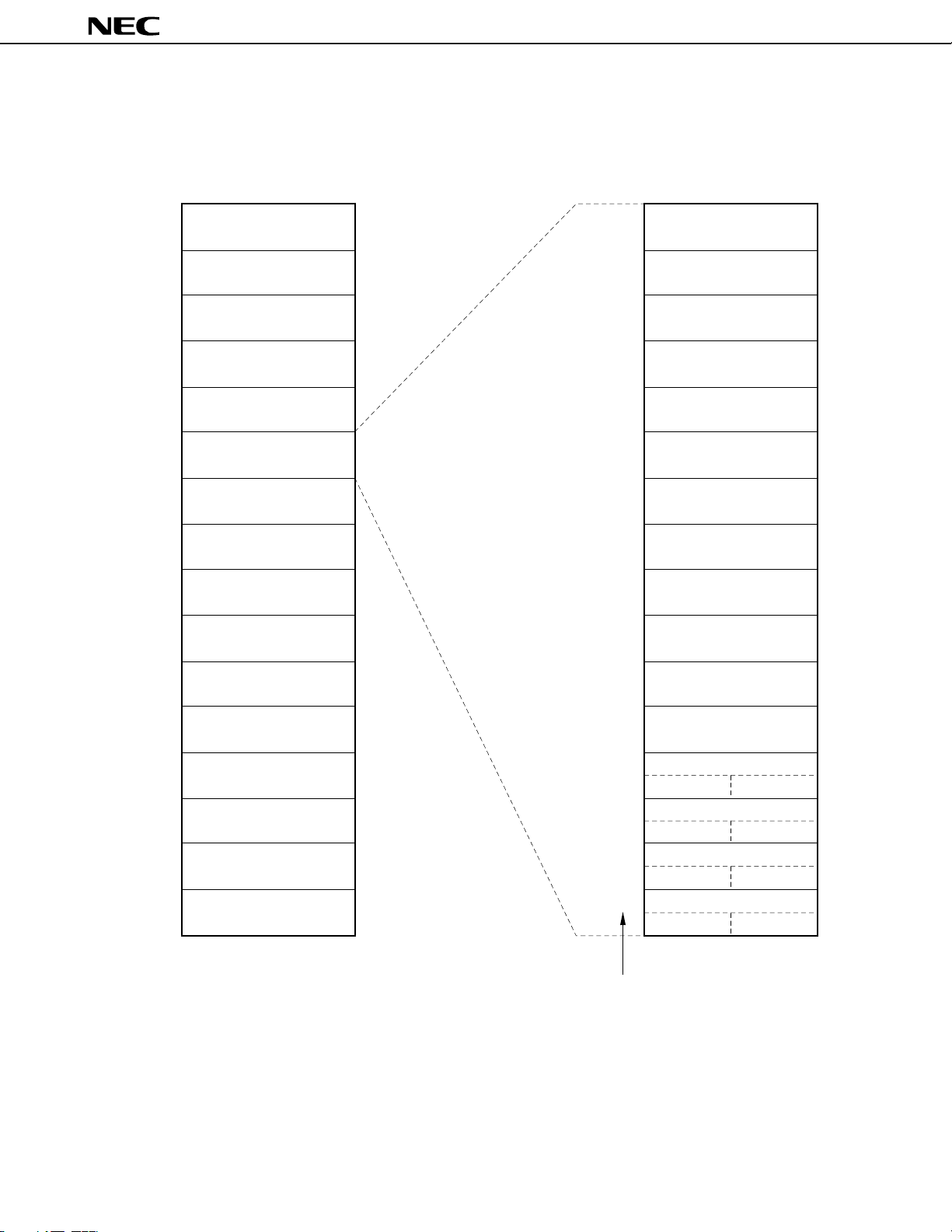
The register bank configuration is shown in Figure 3-1. The general register sets are mapped onto the area with an offset
of (+08H) to (+1FH) from the start address of each register bank. The word address from the start in a register bank is the
extended segment register (DS2) area. The vector PC/DS3 area is used to set the value to be loaded into the PC when
the register bank is switched, that is, the offset value of the start address of the interrupt service routine. This area is also
used as the extended segment register (DS3) area. The PSW save area is used to save the PSW when the register bank
is switched, and the PC save area is used to save the PC when the register bank is switched.
After a reset, register bank 15 is selected automatically. Also, segment register initialization after a reset is performed
for register bank 15 only.
The register file space onto which these general register sets are mapped can also be accessed as data memory by
addition of a special prefix instruction (IRAM:) to a memory manipulation instruction.
Of the 16 set register banks, banks 0 and 1 have macro service channels (parameter and work area for macro service)
allocated in duplicate.
17
000H
020H
040H
060H
080H
0A0H
0C0H
0E0H
100H
120H
140H
160H
180H
1A0H
1C0H
1E0H
1FFH
Register Bank 0
10
11
12
13
14
15
Figure 3-1. Register Bank Configuration
Register File Space (512 bytes)
+00H 15 87 0
1
2
3
4
5
6
7
8
9
+02H
+04H
+06H
+08H
+0AH
+0CH
+0EH
+10H
+12H
+14H
+16H
+18H
+1AH
+1CH
+1EH
DS2
Vector PC/DS3
PSW Save
PC Save
DS0
SS
PS
DS1
IY
IX
BP
SP
BW
BH
DW
DH
CW
CH
AW
AH
µ
PD70433
BL
DL
CL
AL
18
(Offset from the starting address of each register bank)

µ
PD70433
3.2.2 General Registers (AW, BW, CW, DW)
There are four 16-bit general registers. In addition to being accessed as 16-bit registers, these registers can also be
accessed as 8-bit registers by dividing each register into upper and lower 8-bit halves (AH, AL, BH, BL, CH, CL, DH, DL).
These registers are used as 8-bit or 16-bit registers with a wide range of instructions including transfer, arithmetic and
logical operation instructions.
Each register is also used as the default register for specific instruction processing, as shown below.
AW : Word multiplication/division, word input/output, data conversion
AL : Byte multiplication/division, byte input/output, BCD rotation, data conversion
AH : Byte multiplication/division
BW : Data conversion
CW : Loop control branch, repeat prefix
CL : Shift instructions, rotate instructions, BCD operations
DW : Word multiplication/division, indirect addressing input/output
These registers are mapped onto the register file space (in on-chip RAM). The address is the value obtained by adding
the offset for each register to (register bank number × 32).
Table 3-1. General Register Offsets
Register Offset Register Offset
AW 1EH
BW 18H
CW 1CH
DW 1AH
AL 1EH
AH 1FH
BL 18H
BH 19H
CL 1CH
CH 1DH
DL 1AH
DH 1BH
19

µ
PD70433
3.2.3 Pointers (SP, BP) and Index Registers (IX, IY)
These are 16-bit registers used as base pointers or index registers in memory accesses using based addressing (BP),
indexed addressing (IX, IY), based indexed addressing (BP, IX, IY), etc. The SP is also used as the pointer in stack
operations. As with general registers, these are used with transfer instructions, arithmetic operation instructions, etc., but
in this case they cannot be used as 8-bit registers. Each register is also used as the fixed address pointer for specific
instruction processing, as shown below.
SP : Stack manipulation
IX : Block transfers, BCD operation source side address specification
IY : Block transfers, BCD operation destination side address specification
These registers are mapped onto the register file space (in on-chip RAM). The address is the value obtained by adding
the offset for each register to (register bank number × 32).
Table 3-2. Pointer and Index Register Offsets
Register Offset
SP 16H
BP 14H
IX 12H
IY 10H
3.2.4 Segment Registers (PS, SS, DS0, DS1)
The CPU manages the 1M-byte basic memory space by dividing it into 64K-byte units. The CPU specifies the start
address of each segment with a segment register, and uses another register or effective address for the specification of
phyiscal address, with the relative address from the start address as the offset.
The physical address is created as shown below.
Segment Register 4-Bit Fixed
xxxx0H
0xxxxH
+
.... Segment Start Address
.... Offset Value
xxxxxH
There are four segment registers: PS (Program Segment), SS (Stack Segment), DS0 (Data Segment 0), and DS1 (Data
Segment 1). The respective segments are used in the following cases.
PS : Program fetch
SS : Stack manipulation instructions, addressing using BP as base register
DS0 : General variable accesses, source block data accesses such as block transfer instructions, etc.
DS1 : Destination block data accesses such as block transfer instructions, etc.
..... Physical Address (20 Bits)
20

µ
PD70433
However, using a segment override prefix instruction makes it possible for access of general variables to change from
DS0 to another segment register. Also, in addressing which uses BP as the base register, another segment register can
be used instead of SS.
Example MOV AW, 1000H
MOV DS1 : AW
MOV BL, DS1, BYTE PTR [IX]; DSI : Byte data read from IX
When a reset is performed, PS of register bank 15 is initialized to FFFFH, and SS, DS0 and DS1 are initialized to 0000H.
These registers are mapped onto the register file space (in on-chip RAM). The address is the value obtained by adding
the offset for each register to (register bank number × 32).
Table 3-3. Segment Register Offsets
Register Offset
DS0 08H
DS1 0EH
SS 0AH
PS 0CH
3.2.5 Extended Segment Registers (DS2, DS3)
In addition to the segment registers for accessing the 1M-byte basic memory space, the V55PI is provided with extended
segment registers which specify the start address of each 64K-byte segment of the 16M-byte extended memory space.
There are two extended segment registers, DS2 (Data Segment 2) and DS3 (Data Segment 3), which are used as shown
below.
DS2: Extended memory space general variable accesses (by segment override prefix instructions), source block
data accesses in extended memory space block transfer instructions, etc.
DS3: Extended memory space general variable accesses (by segment override prefix instructions), destination
block data accesses in extended memory space block transfer instructions, etc.
The data access using an extended semgnet register is performed by using the segment override prefix. Especially, in
the block transfer instruction, DS2 and DS3 can be specified simultaneously by segment override prefix. (In this case, the
order for DS2 and DS3 is optional.)
Example REP
DS2:
DS3: MOVBKW ; Word memory block transfer from DS2 : IX to DS3 : IY.
The CPU specifies the start address of each segment with an extended segment register, and performs an access by
using another register or effective address for the specification of physical address, with the relative address from the start
address as the offset value.
The physical address is created as shown in the next page.
21

Extended Segment Register 8-Bit Fixed
µ
PD70433
xxxx00H
00xxxxH
+
xxxxxxH
When a reset is performed, DS2 and DS3 of register bank 15 are initialized to 0000H.
These registers are mapped onto the register file space (in on-chip RAM). The address is the value obtained by adding the
offset for each register to (register bank number × 32).
Table 3-4. Extended Segment Register Offsets
Register Offset
... Segment Start Address
... Offset Value
... Physical Address (24 Bits)
DS2 00H
DS3 02H (Also used as vectored PC)
3.2.6 Special Function Registers (SFR)
The V55PI has a group of registers with the function of controlling on-chip peripheral hardware.
A number of registers are provided according to the type of cotrol for each peripheral hardware unit, and the actual
operation can be set using the individual bits in the registers. These registers are mapped onto the memory space, and
are read and written to using the same method as for ordinary memory (see 3.5.3 "Special Function Register Area").
Example MOV AW, 0FFE0H
MOV DS1, AW
MOV BL, DS1 : BYTE PTR [1EFH]; 0FFE0H : 1EFH (PRC register) Read
There are also two instructions, BTCLR and BTCLRL, which are only valid for special function registers. Of these,
BTCLRL is an instruction newly provided in the V25 or V35.
The BTCLR instruction is valid for registers in the upper 240 bytes (0FFF00H to 0FFFEFH) of the special function register
area, and the BTCLRL instruction is valid for registers in the lower 256 bytes (0FFE00H to 0FFEFFH).
22

µ
PD70433
3.3 PROGRAM COUNTER (PC)
This is a 16-bit binary counter which holds the offset value of the program memory address on which the CPU is to perform
execution.
The PC is incremented each time an instruction code is fetched from the instruction queue, and is also loaded with the
new location address value when a branch, call, return or break instruction is executed.
When a reset is performed, 0000H is loaded into the PC. Because the PS register is initialized to FFFFH in a reset, after
a reset the CPU begins execution at physical address 0FFFF0H.
3.4 PROGRAM STATUS WORDS (PSW)
The PSW consists of 6 status flags and 5 control flags.
• Status flags
•V (Overflow) ...Overflow detection flag
•S (Sign) ...Sign bit detection flag
•Z (Zero) ...All zero detection flag
•AC (Auxiliary Carry) ...4-bit carry/borrow detection flag
•P (Parity) ...Parity detection flag
•CY (Carry) ... Carry/borrow detection flag
• Control flags
•RB0 to RB3 (Register Banks 0 to 3) ...Register bankspecification flags
•DIR (Direction) ...Block transfer/input/output instruction direction control flag
•IE (Interrupt Enable) ...Interrupt enabled state control flag
•BRK (Break) ...Single-step interrupt control flag
•IBRK (I/O Break) ...Input/output instruction trap control flag
The status flags are set (1) or reset (0) automatically according to the result (data value) of execution of various kinds
of instructions. The CY flag can be directly set, reset or inverted by an instruction.
The control flags are set or reset by instructions, and control the operation of the CPU. The IE and BRK flags are always
reset when interrupt servicing is initiated.
The contents of the PSW can be saved to and restored from the stack by the PUSH and POP instructions. However,
when the contents are restored by the POP PSW instruction, bits 12 to 15 (RB0 to RB3) are not returned to the PSW.
The low-order 8 bits of the PSW can also be saved to or restored from the AH register by an MOV instruction.
The PSW bit configuration is shown below.
151413121110987654 3210
RB3 RB2 RB1 RB0 Y DIR IE BRK S Z 0 AC 0 P IBRK CY
23
µ
PD70433
3.5 MEMORY SPACE
The V55PI has a 16M-byte memory space. Of this, using lowest 1M bytes (000000H to 0FFFFFH) as the basic memory
space, the 16M bytes including the basic memory space (000000H to FFFFFFH) can be accessed as the extended memory
space. The basic memory space can be accessed using the segment registers (PS, SS, DS0, DS1) in the same way as
in the V25 and V35. The extended memory space can be accessed using the extended segment registers (DS2, DS3), and
has the basic memory space mapped onto the lowest 1M bytes. See 3.2.4 "Segment Registers (PS, SS, DS0, DS1)" and
3.2.5 "Extended Segment Registers (DS2, DS3)" for the physical addresses.
The 496-byte space 0FFE00H to 0FFFEFH has mapped onto it a group of registers to which specific functions are
allocated such as on-chip peripheral hardware registers, control registers, etc., and these are manipulated by memory
accesses.
In addition, independent of these, there is a 512-byte register file space (in on-chip RAM). In addition to being accessed
by using register manipulation instructions as in the V25 and V35, the register file space can also be accessed as data
memory by adding a special prefix instruction (IRAM:) to a memory manipulation in.
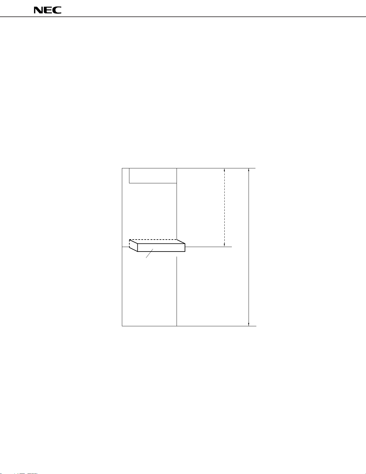
Figure 3-2. Memory Space
000000H
Vector Area
003FFH
Basic Memory
Space
(1M Bytes)
0FFFFFH
100000H
Special Function
Register Area
(On-Chip Area)
FFFFFFH
FFE00H
FFFEFH
Extended Memory
Space (16M Bytes)
3.5.1 Basic Memory Space
The memory space comprises a 1M-byte basic memory space and 16M-byte extended memory space. The basic memory
space is mapped onto the lowest 1M bytes (000000H to 0FFFFFH) of the extended memory space.
The 1M-byte basic memory space is shown in Figure 3-3.
Conditions for accessing the basic memory space by software are the same as for the V20/V30 and V25/V35.
A basic memory space physical address is specified by the segment start address indicated by the segment register (PS,
SS, DS0, DS1) and the offset value from the segment start position indicated by another register or immediate data.
The basic memory space has the vectored interrupt vector area and special function register area mapped onto it. For
an area in which special function registers are mapped, data accesses cannot be made to external memory (program fetches
are possible.)
24

Figure 3-3. Basic Memory Space
µ
PD70433
000000H
Vector Area
1M Bytes
Spaecial Function Register Area
(Internal Area)
0FFFFFH
0FFF0H to 0FFFFFH is a program area used for the system boot, and PS and PC become 0FFFH and 0H, respectively,
therefore the program execution starts from 0FFFF0H.
3.5.2 Extended Memory Space
The 16M-byte extended memory space is shown in Figure 3-4.
The only accesses that can be performed on the extended memory space are data accesses.
The basic memory space is mapped onto the lowest 1M bytes (000000H to 0FFFFFH) of the extended memory space,
and can be accessed using the segment registers PS, SS, DS0 and DS1.
Data accesses can be performed in the extended memory space using the extended segment registers DS2 and DS3.
With DS2 and DS3 it is possible to use a specification as a segment override prefix instruction added to a memory
manipulation instruction.
An extended memory space physical address is specified by the segment start address indicated by the extended
segment register and the offset value from the segment start position indicated by another register or immediate data. If
the generated address indicates the lowest 1M-byte area (000000H to 0FFFFFH), the basic memory space is accessed.
00000H
003FFH
FFE00H
FFFEFH
25
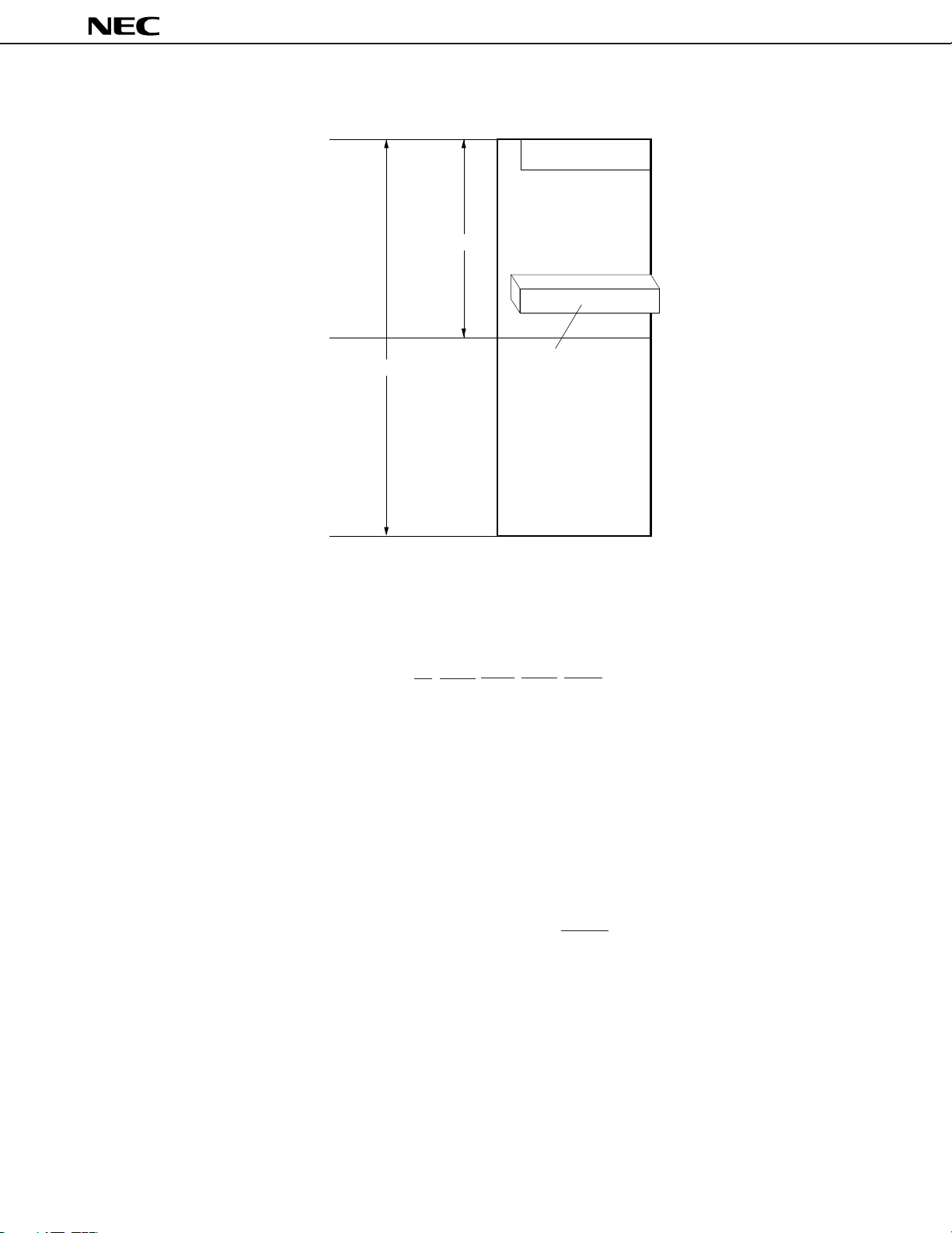
Figure 3-4. Extended Memory Space
µ
PD70433
000000H
0FFFFFH
100000H
FFFFFFH
16M Bytes
Vector Area
1M Bytes
Spaecial Function
Register Area
(Internal Area)
00000H
003FFH
FFE00H
FFFEFH
3.5.3 Special Function Register Area
The 496-byte space 0FFE00H to 0FFFEFH has mapped onto it a group of registers to which functions such as
on-chip peripheral hardware operation specification, status monitoring, etc., are assigned.
Program fetches cannot be performed from these areas.
Special function register manipulation is performed by accesses by means of memory manipulation instructions.
If the special function register area is accessed, RD, WRH, WRL, IORD, IOWR and other control signals do not become
active.
A list of special function registers is given in Table 3-5. The meaning of the items in the table is explained below.
• Symbol............................ The symbol used to indicate the special function register name. Corresponds to the
operand description format (symbol name) in a memory manipulation instruction.
• R/ W ................................. Indicates whether this special function register is read/write enabled.
R/W : Read/write enabled
R : Read only
W : Write only
• Manipulation Method ..... Indicates which of the following can be used on the register: bit manipulation,
8-bit manipulation, 16-bit manipulation, 32-bit manipulation.
• RESET............................ Indicates the status of the register after RESET input.
Note Addresses which are not listed are the reserved area, therefore, they should not be accessed by the user
program.
26
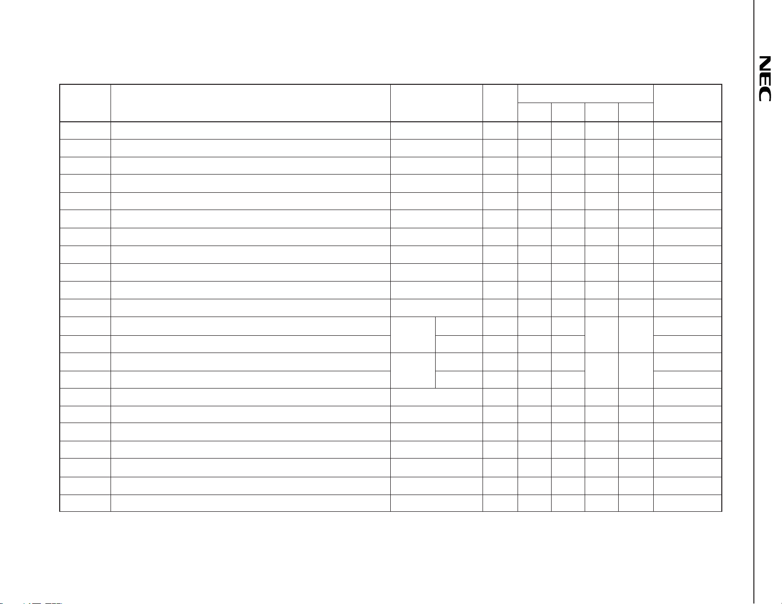
Table 3-5. Special Function Registers (1/7)
27
Address Special Function Register Name Symbol R/W After Reset
0FFE00H A/D conversion result register 0 ADCR0 R
0FFE02H A/D conversion result register 1 ADCR1 R
0FFE04H A/D conversion result register 2 ADCR2 R
0FFE06H A/D conversion result register 3 ADCR3 R
0FFE10H Parallel interface buffer PAD R/W *1
0FFE18H Parallel interface control register 0 PAC0 R/W
0FFE19H Parallel interface control register 1 PAC1 R/W
0FFE1AH Parallel interface status register PAS R/W *2
0FFE1CH Parallel interface acknowledge interval register 1 PAI1 W
0FFE1DH Parallel interface acknowledge interval register 2 PAI2 W
0FFE20H A/D converter mode register ADM R/W
0FFEC0H Interrupt mask flag register 0 (low) MK0L R/W
0FFEC1H Interrupt mask flag register 0 (high) MK0H R/W
0FFEC2H Interrupt mask flag register 1 (low) MK1L R/W
0FFEC3H Interrupt mask flag register 1 (high) MK1H R/W
0FFEC4H In-service priority register ISPR R
0FFEC5H Interrupt mode control register IMC R/W
0FFEC9H Interrupt request control register 09 IC09 R/W
0FFECAH Interrupt request control register 10 IC10 R/W
0FFECBH Interrupt request control register 11 IC11 R/W
0FFECCH Interrupt request control register 12 IC12 R/W
0FFECDH Interrupt request control register 13 IC13 R/W
*1.Varies according to input/output mode.
2. Some bits R, others R/W (possible).
MK0
MK1
Manipulable Bit Units
1 Bit 8 Bits 16 Bits 32 Bits
•
•
•
•
•
••
••
•
•
•
••
••
•
••
••
•
••
••
•
••
••
••
••
••
Undefined
Undefined
Undefined
Undefined
Undefined
90H
03H
40H
Undefined
Undefined
00H
FFH
FFH
FFH
FFH
00H
80H
43H
43H
43H
43H
43H
µ
PD70433

28
Table 3-5. Special Function Registers (2/7)
Address Special Function Register Name Symbol R/W After Reset
0FFECEH Interrupt request control register 14 IC14 R/W
0FFED0H Interrupt request control register 16 IC16 R/W
0FFED1H Interrupt request control register 17 IC17 R/W
0FFED2H Interrupt request control register 18 IC18 R/W
0FFED3H Interrupt request control register 19 IC19 R/W
0FFED4H Interrupt request control register 20 IC20 R/W
0FFED5H Interrupt request control register 21 IC21 R/W
0FFED6H Interrupt request control register 22 IC22 R/W
0FFED7H Interrupt request control register 23 IC23 R/W
0FFED8H Interrupt request control register 24 IC24 R/W
0FFED9H Interrupt request control register 25 IC25 R/W
0FFEDAH Interrupt request control register 26 IC26 R/W
0FFEDBH Interrupt request control register 27 IC27 R/W
0FFEDCH Interrupt request control register 28 IC28 R/W
0FFEDDH Interrupt request control register 29 IC29 R/W
0FFEDEH Interrupt request control register 30 IC30 R/W
0FFEDFH Interrupt request control register 31 IC31 R/W
0FFEE0H Interrupt request control register 32 IC32 R/W
0FFEE4H Interrupt request control register 36 IC36 R/W
0FFEE5H Interrupt request control register 37 IC37 R/W
0FFF00H Port 0 P0 R/W
0FFF01H Port 1 P1 R
0FFF02H Port 2 P2 R/W
0FFF03H Port 3 P3 R/W
Manipulable Bit Units
1 Bit 8 Bits 16 Bits 32 Bits
••
••
••
••
••
••
••
••
••
••
••
••
••
••
••
••
••
••
••
••
••
••
••
••
43H
43H
43H
43H
43H
43H
43H
43H
43H
43H
43H
43H
43H
43H
43H
43H
43H
43H
43H
43H
Undefined
Undefined
Undefined
Undefined
µ
PD70433
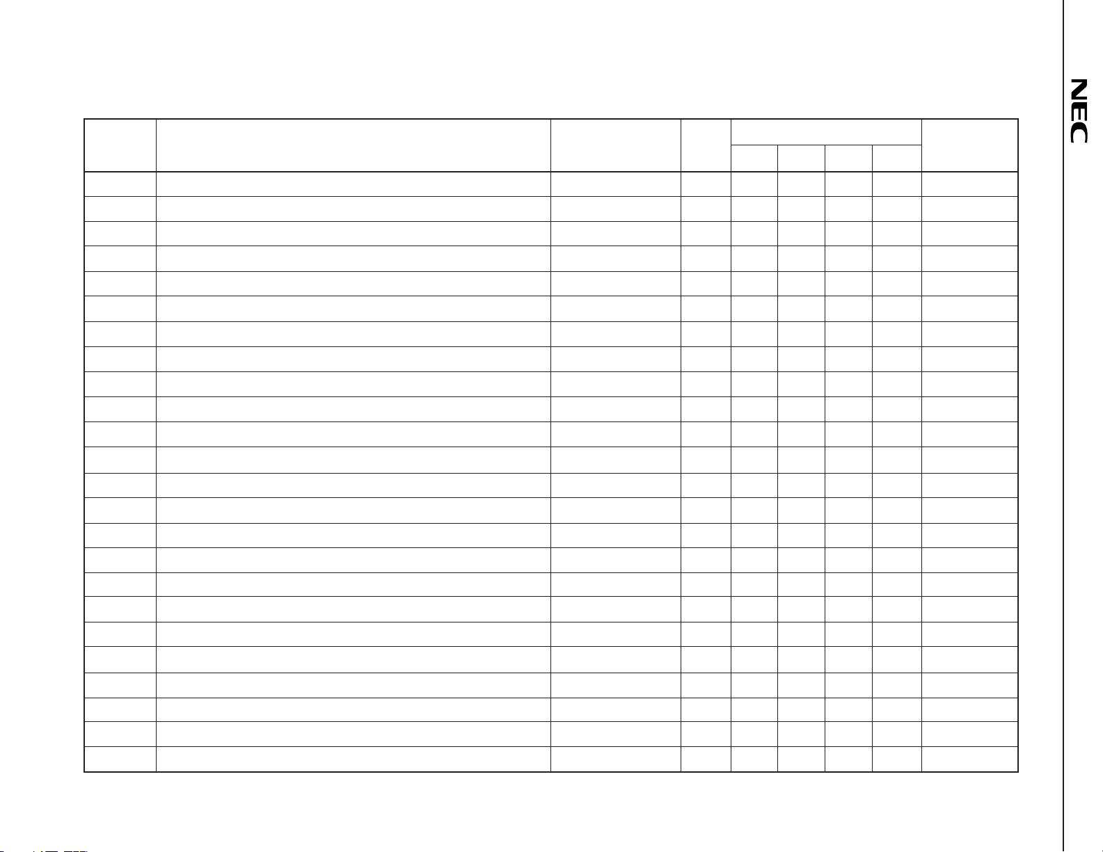
Table 3–5. Special Function Registers (3/7)
29
Address Special Function Register Name Symbol R/W After Reset
0FFF04H Port 4 P4 R/W
0FFF05H Port 5 P5 R/W
0FFF06H Port 6 P6 R
0FFF07H Port 7 P7 R/W
0FFF08H Port 8 P8 R/W
0FFF0CH Port read control register PRDC R/W
0FFF0EH Real–time output port RTP R/W
0FFF10H Port 0 mode register PM0 R/W
0FFF12H Port 2 mode register PM2 R/W
0FFF13H Port 3 mode register PM3 R/W
0FFF14H Port 4 mode register PM4 R/W
0FFF15H Port 5 mode register PM5 R/W
0FFF17H Port 7 mode register PM7 R/W
0FFF18H Port 8 mode register PM8 R/W
0FFF22H Port 2 mode conrol register PMC2 R/W
0FFF23H Port 3 mode control register PMC3 R/W
0FFF24H Port 4 mode control register PMC4 R/W
0FFF25H Port 5 mode control register PMC5 R/W
0FFF27H Port 7 mode control register PMC7 R/W
0FFF28H Port 8 mode control register PMC8 R/W
0FFF2CH Real–time output port control register RTPC R/W
0FFF2DH Real–time output port delay specification register RTPD R/W
0FFF2EH Port 7 buffer (low) P7L R/W
0FFF2FH Port 7 buffer (high) P7H R/W
Manipulable Bit Units
1 Bit 8 Bits 16 Bits 32 Bits
••
••
••
••
••
••
••
••
••
••
••
••
••
••
••
••
••
••
••
••
••
••
••
••
Undefined
Undefined
Undefined
Undefined
Undefined
00H
Undefined
FFH
FFH
FFH
FFH
FFH
FFH
FFH
00H
00H
00H
00H
00H
00H
40H
Undefined
Undefined
Undefined
µ
PD70433

30
Table 3-5. Special Function Registers (4/7)
Address Special Function Register Name Symbol R/W After Reset
0FFF30H Timer control register 0 TMC0 R/W
0FFF31H Timer control register 1 TMC1 R/W
0FFF32H Timer output control register 0 TOC0 R/W
0FFF33H Timer output control register 1 TOC1 R/W
0FFF34H External interrupt mode register 0 INTM0 R/W
INTM
0FFF35H External interrupt mode register 1 INTM1 R/W
0FFF40H Timer register 0 TM0 R/W
0FFF42H Timer register 1 TM1 R/W
0FFF44H Timer register 2 TM2 R/W
0FFF46H Timer register 3 TM3 R/W
0FFF48H Timer capture register 00 CT00 R/W
0FFF4AH Timer capture register 01 CT01 R/W
0FFF4CH Timer compare register 00 CM00 R/W
0FFF4EH Timer compare register 01 CM01 R/W
0FFF50H Timer capture register 10 CT10 R/W
0FFF52H Timer compare register 10 CM10 R/W
0FFF54H Timer compare register 11 CM11 R/W
0FFF58H Timer compare register 20 CM20 R/W
0FFF5AH Timer compare register 21 CM21 R/W
0FFF5CH Timer compare register 22 CM22 R/W
0FFF5EH Timer compare register 23 CM23 R/W
0FFF60H Watchdog timer mode register WDM R/W*
0FFF64H Timer compare register 30 CM30 R/W
* WDT can only be written to by the RSTWDT instruction (8-bit unit only).
Manipulable Bit Units
1 Bit 8 Bits 16 Bits 32 Bits
••
•
••
••
•
••
••
•
••
•
•
•
•
•
•
•
•
•
•
•
•
•
•
•
••
•
Undefined
Undefined
Undefined
Undefined
Undefined
Undefined
Undefined
Undefined
Undefined
Undefined
Undefined
Undefined
00H
00H
00H
00H
00H
00H
00H
00H
00H
00H
µ
PD70433
00H
 Loading...