DATA SHEET
MOS INTEGRATED CIRCUIT
µ
PD6P4B
4-BIT SINGLE-CHIP MICROCONTROLLER
FOR INFRARED REMOTE CONTROL TRANSMISSION
DESCRIPTION
The µPD6P4B is a microcontroller for infrared remote control transmitters which is provided with a one-time
PROM as the program memory.
Because users can write programs for the µPD6P4B, it is ideal for program evaluation and small-scale production
µ
of the application systems using the
When reading this document, also refer to the µPD62 Data Sheet (U14208E) and the µPD63, 63A, 64 Data
Sheet (U11371E).
PD62, 63, 63A, or 64.
FEATURES
• Program memory (one-time PROM): 1002 × 10 bits
• Data memory (RAM) : 32 × 4 bits
• Built-in carrier generation circuit for infrared remote control
• 9-bit programmable timer : 1 channel
µ
• Command execution time : 16
• Stack level : 1 level (Stack RAM is for data memory RF as well.)
• I/O pins (KI/O) : 8 units
• Input pins (K
• Sense input pin (S0) : 1 unit
•S1/LED pin (I/O) : 1 unit (In output mode, this is the remote control transmission display
• Power supply voltage : V
• Operating ambient temperature : T
• Oscillator frequency : fX = 2.4 to 8 MHz
• POC circuit
APPLICATION
Infrared remote control transmitter (for AV and household electric appliances)
I) : 4 units
s (when operating at fX = 4 MHz: ceramic oscillation)
pin.)
DD = 2.2 to 3.6 V (at fX = 4 MHz)
VDD = 2.7 to 3.6 V (at fX = 8 MHz)
A = –40 to +85 °C
The information in this document is subject to change without notice. Before using this document, please
confirm that this is the latest version.
Not all devices/types available in every country. Please check with local NEC representative for availability
and additional information.
Document No. U13594EJ2V0DS00 (2nd edition)
Date Published May 1999 N CP(K)
Printed in Japan
The mark shows major revised points.
©
1998,1999

ORDERING INFORMATION
Part Number Package
µ
PD6P4BGS 20-pin plastic SOP (300 mil)
µ
PD6P4BMC-5A4 20-pin plastic SSOP (300 mil)
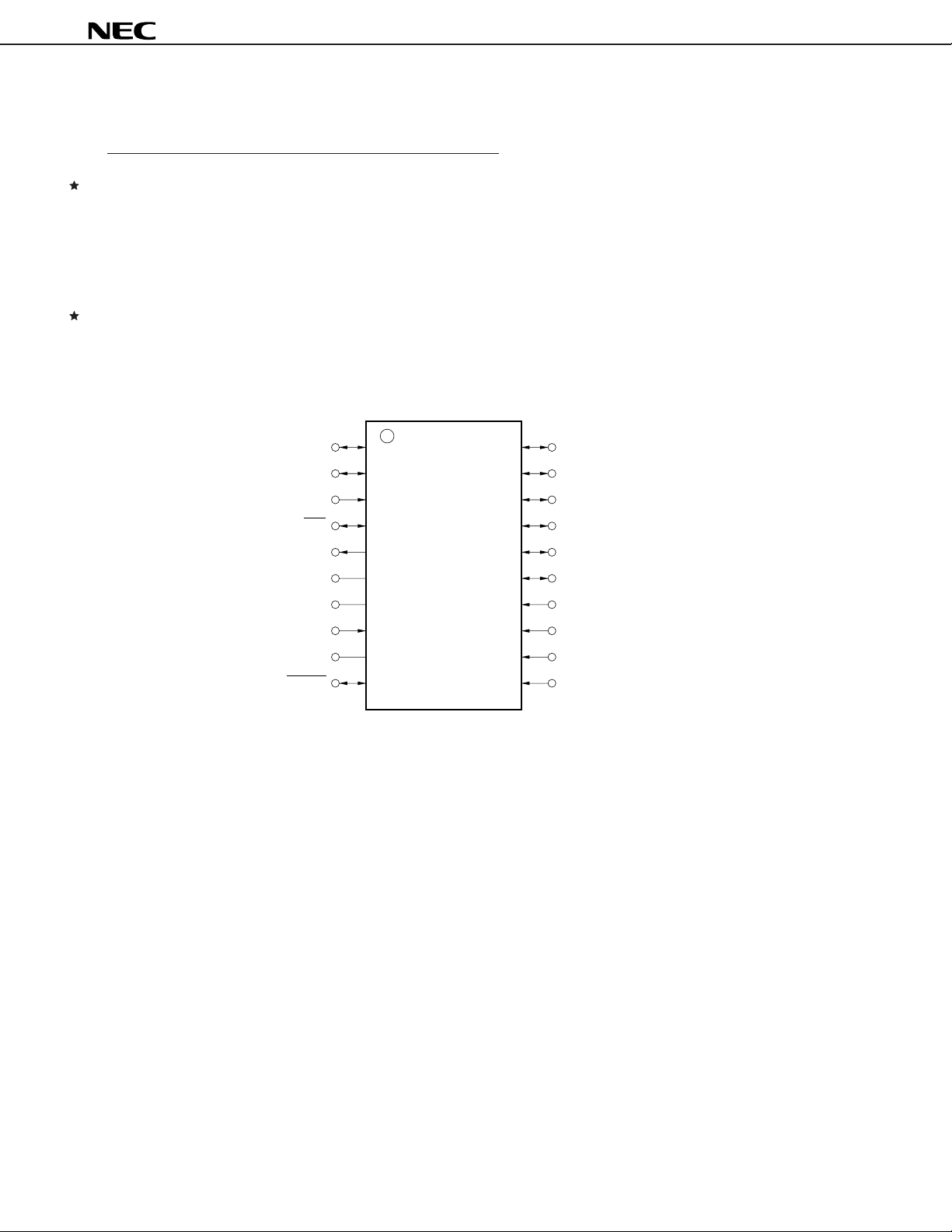
PIN CONFIGURATION (TOP VIEW)
20-pin Plastic SOP (300 mil)
• µPD6P4BGS
20-pin Plastic SSOP (300 mil)
µ
PD6P4BMC-5A4
•
(1) Normal operating mode
µ
PD6P4B
K
I/O6
KI/O7
S0
S1/LED
REM
V
XOUT
XIN
GND
RESET
1
2
3
4
5
DD
6
7
8
9
10
20
19
18
17
16
15
14
13
12
11
K
I/O5
KI/O4
KI/O3
KI/O2
KI/O1
KI/O0
KI3
KI2
KI1
KI0
2
Data Sheet U13594EJ2V0DS00

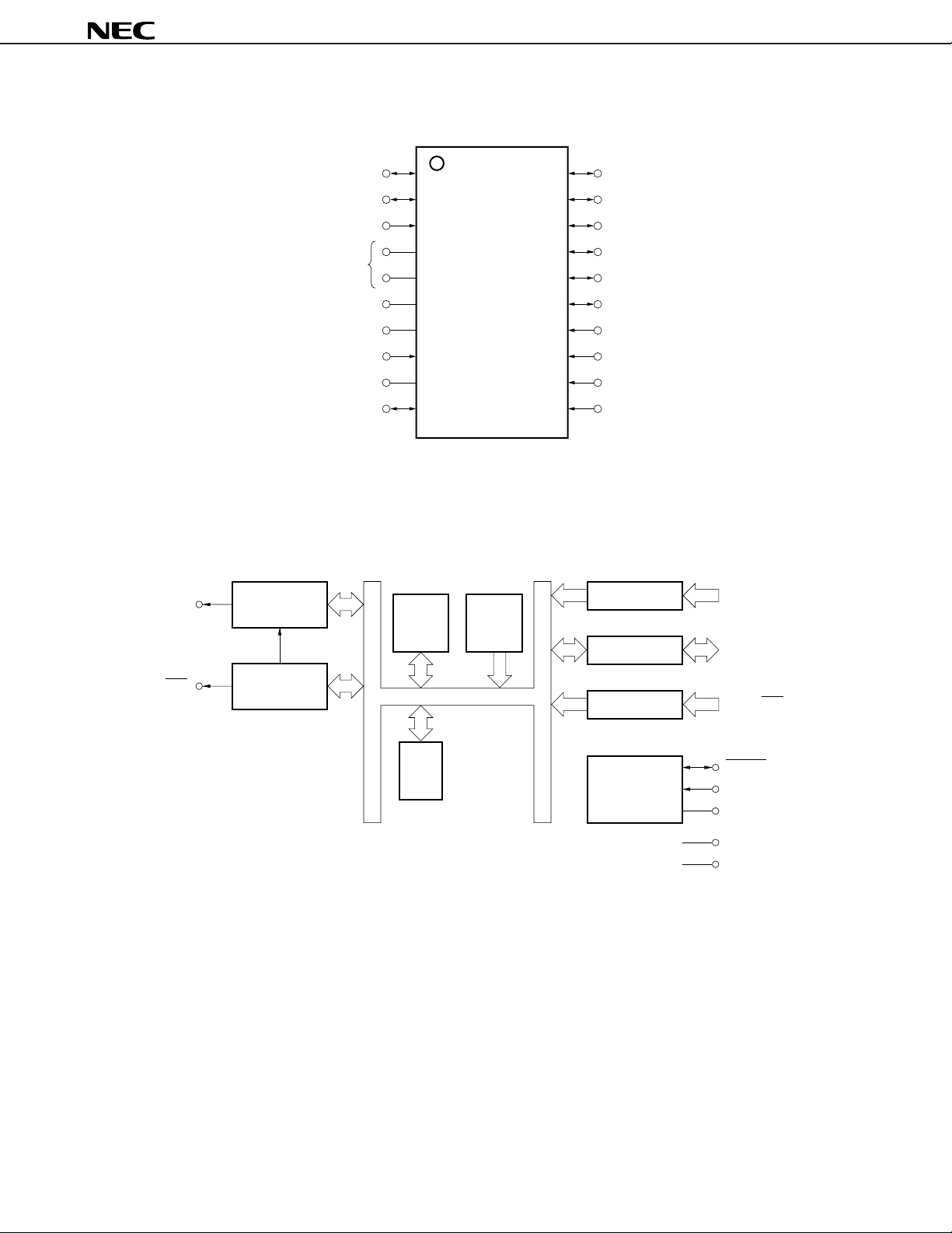
(2) PROM programming mode
D
D
CLK
(L)
V
X
OUT
X
GND
V
6
7
DD
IN
PP
1
2
3
4
5
6
7
8
9
10
20
19
18
17
16
15
14
13
12
11
D
D
D
D
D
D
MD
MD
MD
MD
5
4
3
2
1
0
3
2
1
0
Caution Round brackets ( ) indicate the pins not used in the PROM programming mode.
L : Connect each of these pins to GND via a pull-down resistor.
µ
PD6P4B
BLOCK DIAGRAM
CARRIER
GENERATOR
S
REM
1
/LED
9-bit
TIMER
CPU
CORE
RAM
ONETIME
PROM
4
8
2
PORT K
PORT K
I/O
PORT S
SYSTEM
CONTROL
4
KI0-K
I
8
2
I3
K
I/O0-KI/O7
S0, S1/LED
RESET
IN
X
X
OUT
V
DD
GND
Data Sheet U13594EJ2V0DS00
3

LIST OF FUNCTIONS
µ
PD6P4B
Item
ROM capacity 1002 × 10 bits
One-time PROM
RAM capacity 32 × 4 bits
Stack 1 level (shared with RF of RAM)
I/O pin Key input (KI) : 4 pins
Key I/O (KI/O) : 8 pins
Key expansion input (S0, S1) : 2 pins
Remote control transmitter display output (LED) : 1 pin (shared with S1 pin)
Number of keys 32 keys
48 keys (when expanded by key expansion input)
96 keys (when expanded by key expansion input and diode)
Clock frequency Ceramic oscillation
fX = 2.4 to 4 MHz
fX = 4 to 8 MHz
Instruction execution time 16 µs (at fX = 4 MHz)
Carrier frequency fX/8, fX/16, fX/64, fX/96, fX/128, fX/192, no carrier (high level)
Timer 9-bit programmable timer : 1 channel
POC circuit Provided
Note
µ
PD6P4B
Supply voltage VDD = 2.2 to 3.6 V (fX = 2.4 to 4 MHz), VDD = 2.7 to 3.6 V (fX = 4 to 8 MHz)
Operating ambient • TA = –40 to +85 °C
temperature • TA = –20 to +70 °C (when using POC circuit)
Package • 20-pin plastic SOP (300 mil)
• 20-pin plastic SSOP (300 mil)
Note It is necessary to design the application circuit so that the RESET pin goes low at a supply voltage of less
than 2.7 V.
4
Data Sheet U13594EJ2V0DS00

µ
PD6P4B
TABLE OF CONTENTS
1. PIN FUNCTIONS......................................................................................................................... 6
1.1 Normal Operating Mode.................................................................................................................... 6
1.2 PROM Programming Mode............................................................................................................... 7
1.3 INPUT/OUTPUT Circuits of Pins ...................................................................................................... 8
1.4 Dealing with Unused Pins ................................................................................................................ 9
1.5 Notes on Using K
I Pin at Reset ........................................................................................................ 9
2. DIFFERENCES AMONG µPD62, 63, 63A, 64, AND µPD6P4B ................................................. 10
2.1 Program Memory (One-time PROM) ................................................................................................ 11
3. WRITING AND VERIFYING ONE-TIME PROM (PROGRAM MEMORY) .................................. 12
3.1 Operating Mode When Writing/Verifying Program Memory.......................................................... 12
3.2 Program Memory Writing Procedure .............................................................................................. 13
3.3 Program Memory Reading Procedure.............................................................................................14
4. ELECTRICAL SPECIFICATIONS............................................................................................... 15
5. CHARACTERISTIC CURVE (REFERENCE VALUES) .............................................................. 21
6. APPLIED CIRCUIT EXAMPLE ................................................................................................... 23
7. PACKAGE DRAWINGS..............................................................................................................24
8. RECOMMENDED SOLDERING CONDITIONS.......................................................................... 26
APPENDIX A. DEVELOPMENT TOOLS ........................................................................................ 27
APPENDIX B. EXAMPLE OF REMOTE-CONTROL TRANSMISSION FORMAT .......................... 28
Data Sheet U13594EJ2V0DS00
5

µ
PD6P4B
1. PIN FUNCTIONS
1.1 Normal Operating Mode
Pin No. Symbol Function Output Format When Reset
1KI/O0-KI/O7 CMOS High-level output
2 push-pull
15-20
3S0 — High-impedance
4S1/LED CMOS push-pull High-level output
5 REM CMOS push-pull Low-level output
6VDD ——
7XOUT — Low level
8XIN (oscillation stopped)
9 GND ——
10 RESET ——
11-14 KI0-KI3
These pins refer to the 8-bit I/O ports. I/O switching can
be made in 8-bit units.
In INPUT mode, a pull-down resistor is added.
In OUTPUT mode, they can be used as the key scan
output of the key matrix.
Refers to the input port.
Can also be used as the key return input of the key
matrix.
In INPUT mode, the availability of the pull-down resistor
of the S0 and S1 ports can be specified by software in
terms in 2-bit units.
If INPUT mode is canceled by software, this pin is placed
in OFF mode and enters the high-impedance state.
Refers to the I/O port.
In INPUT mode (S1), this pin can also be used as the key
return input of the key matrix.
The availability of the pull-down resistor of the S0 and S1
ports can be specified by software in 2-bit units.
In OUTPUT mode (LED), it becomes the remote control
transmission display output (active low). When the
remote control carrier is output from the REM output, this
pin outputs the low level from the LED output synchronously
with the REM signal.
Refers to the infrared remote control transmission output.
The output is active high.
Carrier frequency: fX/8, fX/64, fX/96, high-level,
fX/16, fX/128, fX/192 (usable on software)
Refers to the power supply.
These pins are connected to system clock ceramic
resonators.
Refers to the ground.
Normally, this pin is a system reset input. By inputting
a low level, the CPU can be reset. When resetting with
the POC circuit a low level is output. A pull-up resistor
is incorporated.
Note 2
These pins refer to the 4-bit input ports.
They can be used as the key return input of the key
matrix.
The use of the pull-down resistor can be specified by
software in 4-bit units.
Note 1
(OFF mode)
(LED)
— Input (low-level)
Notes 1. Be careful about this because the drive capability of the low-level output side is held low.
2. In order to prevent malfunction, be sure to input a low level to more than one of pins KI0 to KI3 when
reset is released (when RESET pin changes from low level to high level, or POC is released due to
supply voltage startup).
6
Data Sheet U13594EJ2V0DS00

µ
1.2 PROM Programming Mode
Pin No. Symbol Function I/O
1, 2 D0-D7 8-bit data input/output when writing/verifying program memory I/O
15-20
3 CLK Clock input for updating address when writing/verifying program Input
memory
6VDD Power Supply. –
Supply +6 V to this pin when writing/verifying program memory.
7XOUT Clock necessary for writing program memory. Connect 4 MHz ceramic –
8XIN resonator to these pins. Input
9 GND GND –
10 VPP Supplies voltage for writing/verifying program memory. –
Apply +12.5 V to this pin.
11-14 MD0-MD3 Input for selecting operation mode when writing/verifying program memory. Input
PD6P4B
Data Sheet U13594EJ2V0DS00
7

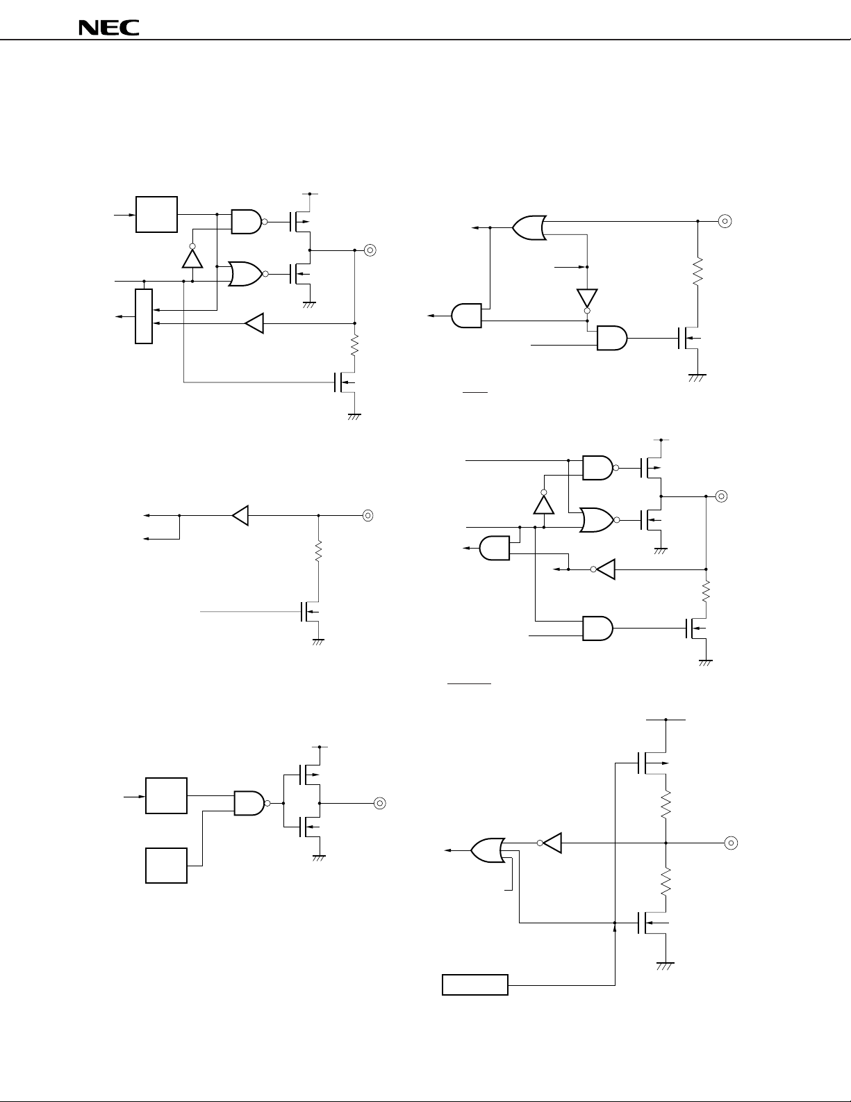
1.3 INPUT/OUTPUT Circuits of Pins
The input/output circuits of the µPD6P4B pins are shown in partially simplified forms below.
I/O0-KI/O7 (4) S0
(1) K
V
DD
data
Output
latch
P-ch
Input buffer
µ
PD6P4B
output
disable
Selector
Input buffer
Note The drive capability is held low.
I0-KI3
(2) K
standby
release
Input buffer
pull-down flag
N-ch
N-ch
Note
N-ch
standby
release
REM
output latch
pull-down flag
(5) S1/LED
output
disable
standby
release
pull-down flag
OFF mode
Input buffer
V
N-ch
DD
P-ch
N-ch
N-ch
(3) REM (6) RESET
VDD
P-ch
data
8
Output
latch
N-ch
Carrier
generator
Internal reset signal
other than POC
Data Sheet U13594EJ2V0DS00
POC circuit
Input buffer
V
DD
P-ch
N-ch

1.4 Dealing with Unused Pins
The following connections are recommended for unused pins in the normal operation mode.
Table 1-1. Connections for Unused Pins
µ
PD6P4B
Pin
KI/O INPUT mode — Open
OUTPUT mode High-level output
REM —
S1/LED OUTPUT mode (LED) setting
S0 OFF mode setting Directly connected to GND
KI —
Note
RESET
Inside the microcontroller Outside the microcontroller
Built-in POC circuit Open
Connection
Note If the circuit is an applied one requiring high reliability, be sure to design it in such a manner that the RESET
signal is entered externally.
Caution The I/O mode and the terminal output level are recommended to be fixed by setting them
repeatedly in each loop of the program.
1.5 Notes on Using KI Pin at Reset
In order to prevent malfunction, be sure to input a low level to more than one of pins KI0 to KI3 when reset is
released (when RESET pin changes from low level to high level, or POC is released due to supply voltage startup).
Data Sheet U13594EJ2V0DS00
9

µ
PD6P4B
2. DIFFERENCES AMONG µPD62, 63, 63A, 64, AND µPD6P4B
Table 2-1 shows the differences among the µPD62, 63, 63A, 64, and µPD6P4B.
The only differences among these models are the program memory, supply voltage, system clock frequency,
oscillation stabilization wait time, and POC circuit (mask option), and the CPU function and internal peripheral
hardware are the same.
The electrical characteristics also differ slightly. For the electrical characteristics, refer to the Data Sheet of each
model.
µ
Table 2-1. Differences among
(1) When POC circuit (mask option) is provided to
PD62, 63, 63A, 64, and µPD6P4B
µ
PD62, 63, 63A, and 64
Item
ROM One-time PROM Mask ROM
Oscillation stabilization wait time
• On releasing STOP mode by release 286/fX 52/fX
condition
• On releasing STOP or HALT mode by 478/fX to 926/fX 246/fX to 694/fX
RESET input and at reset
VPP pin and operating mode select pin Provided Not provided
Electrical specifications Some electrical specifications, such as data retention voltage and current
µ
PD6P4B
1002 × 10 bits 512 × 10 bits 768 × 10 bits 1002 × 10 bits
(000H to 3E9H) (000H to 1FFH) (000H to 2FFH) (000H to 3E9H)
consumption, differ. For details, refer to Data Sheet of each model.
µ
PD62, 63
µ
PD63A
µ
PD64
(2) When POC circuit (mask option) is not provided to µPD62, 63, 63A, and 64
Item
ROM One-time PROM Mask ROM
Oscillation stabilization wait time
• On releasing STOP mode by release 286/fX 52/fX
condition
• On releasing STOP or HALT mode by 478/fX to 926/fX 246/fX to 694/fX
RESET input and at reset
VPP pin and operating mode select pin Provided Not provided
POC circuit Incorporated Not provided
Supply voltage
System clock frequency
Electrical specifications Some electrical specifications, such as data retention voltage and current
µ
PD6P4B
1002 × 10 bits 512 × 10 bits 768 × 10 bits 1002 × 10 bits
(000H to 3E9) (000H to 1FFH) (000H to 2FFH) (000H to 3E9H)
VDD = 2.2 to 3.6 V
(TA = –40 to +85 °C)
•fX = 2.4 to 4 MHz
•fX = 4 to 8 MHz
consumption, differ. For details, refer to Data Sheet of each model.
µ
PD62, 63
VDD = 1.8 to 3.6 V (TA = –40 to +85 °C)
•fX = 2.4 to 4 MHz
Note
• fX = 2.4 to 8 MHz (VDD = 2.2 to 3.6 V)
µ
PD63A
µ
PD64
Note It is necessary to design the application circuit so that the RESET pin goes low when the supply voltage
is less than 2.7 V.
10
Data Sheet U13594EJ2V0DS00
 Loading...