NEC UPD6708GS, UPD6708CX Datasheet
DATA SHEET
MOS INTEGRATED CIRCUIT
µ
PD6708
IEBus (Inter Equipment Bus) PROTOCOL CONTROL LSI
DESCRIPTION
The µPD6708 is a peripheral LSI for microcontrollers that controls the protocol of the IEBus.
This LSI processes the protocol of the IEBus. Because it is provided with a transmit/receive buffer, the microcontroller
can concentrate on the application processing of the IEBus. Because the µPD6708 also contains an IEBus driver/receiver,
it can be directly connected to the bus.
FEATURES
• Protocol control of IEBus
• Multi-master system
• Broadcast communication function (communication between one unit and multiple units)
• Choice of three modes with different transmission speeds
At 12 MHz At 12.58 MHz
Mode 0 Approx. 3.9 Kbps Approx. 4.1 Kbps
Mode 1 Approx. 17 Kbps Approx. 18 Kbps
Mode 2 Approx. 26 Kbps Approx. 27 Kbps
• On-chip IEBus driver/receiver
• Transmit/receive buffer
Transmit: 4-byte FIFO
Receive: 20-byte FIFO
• Interface with microcontroller
• Three-line serial I/O (SCK, SO, SI pins)
• Transfer with MSB first
• Oscillation frequency (f
• In modes 0 and 1: ±1.5 %
• In mode 2: ±0.5 %
• Supply voltage: V
X): 12 MHz, 12.58 MHz
DD = 5 V ±10 %
ORDERING INFORMATION
Part Number Package
µ
PD6708CX 16-pin plastic DIP (300 mil)
µ
PD6708GS 16-pin plastic SOP (300 mil)
APPLICATION FIELD
Fields where a small-scale digital data transfer system is required between equipment, such as automobile electronic
systems and industrial equipment
Document No. U10680EJ2V0DS00 (2nd edition)
(Previous No. IC-3282)
Date Published January 1996 P
Printed in Japan
The information in this document is subject to change without notice.
The mark ★ shows major revised points.
©
1993
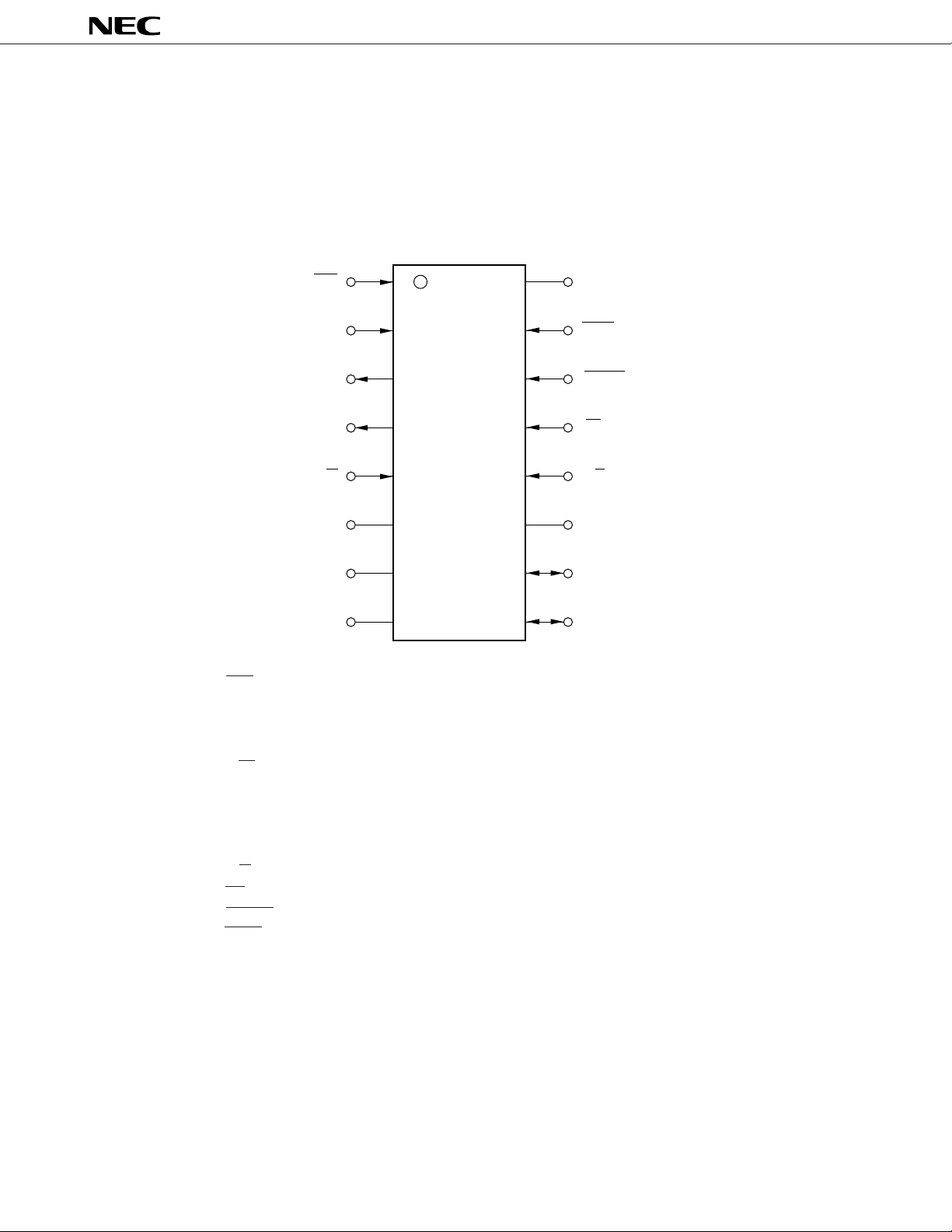
PIN CONFIGURATION (TOP VIEW)
• 16 pin plastic DIP (300 mil)
µ
PD6708CX
• 16 pin plastic SOP (300 mil)
µ
PD6708GS
µ
PD6708
SCK
SO
IRQ
R/W
XO
GND
1
SI
XI
2
3
4
5
6
7
8
16
15
14
13
12
11
10
V
DD
TEST
RESET
CS
C/D
DD
AV
BUS+
9
BUS–
SCK : Serial clock input
SI : Serial data input
SO : Serial data output
IRQ : Interrupt request output
R/W : Read/write switchover input
XI, XO : System clock
GND : Ground
BUS–, BUS+ : IEBus input/output
AVDD : IEBus analog power supply (connected to VDD pin)
C/D : Command/data switchover input
CS : Chip select input
RESET : Reset input
TEST : Test input (connected to VDD pin)
DD : Positive power supply
V
2

µ
PD6708
CONTENTS
1. PIN FUNCTIONS......................................................................................................................................... 5
1.1 List of Pin Functions ......................................................................................................................................... 5
2. IEBus OPERATION .................................................................................................................................... 6
2.1 Operation Overview ........................................................................................................................................... 6
2.2 IEBus Communication Protocol ...................................................................................................................... 7
2.2.1 Bus mastership determination (arbitration) ................................................................................... 8
2.2.2 Communication modes ...................................................................................................................... 8
2.2.3 Communication address ................................................................................................................... 9
2.2.4 Broadcast communication ................................................................................................................ 9
2.3 Transfer Protocol ............................................................................................................................................. 10
2.4 Transfer Data (Contents of Data Field)......................................................................................................... 16
2.5 Bit Format ......................................................................................................................................................... 19
3. INTERNAL CONFIGURATION................................................................................................................. 20
3.1 Data Link Layer Controller ............................................................................................................................. 21
3.2 Physical Layer Controller ............................................................................................................................... 21
3.3 IEBus Driver/Receiver ..................................................................................................................................... 2 1
3.4 Host Interface ................................................................................................................................................... 21
4. INTERFACING WITH HOST CONTROLLER .......................................................................................... 22
4.1 Accessible Buffers and Registers from Host Controller ........................................................................... 22
4.1.1 Write data buffer (WDB) .................................................................................................................. 22
4.1.2 Read data buffer (RDB) ................................................................................................................... 2 2
4.1.3 Command register (CMR)................................................................................................................ 22
4.1.4 Status register (STR) ....................................................................................................................... 23
4.2 Host Interface Modes ...................................................................................................................................... 23
4.2.1 Switching through pin control ....................................................................................................... 24
4.2.2 Switching through software control.............................................................................................. 26
4.3 Reset Mode ....................................................................................................................................................... 28
5. COMMUNICATION CONTROL COMMANDS ......................................................................................... 30
5.1 Overview of Communication Control Commands....................................................................................... 30
5.2 Communication Control Command Functions............................................................................................ 31
5.2.1 INIT command (command code: 0000) .......................................................................................... 31
5.2.2 SETSA command (command code: 0001) .................................................................................... 32
5.2.3 MREQ1 command (command code: 0010) ................................................................................... 33
5.2.4 MREQ2 command (command code: 0011) ................................................................................... 34
5.2.5 ABORT command (command code: 0100) ................................................................................... 34
5.2.6 SETSD command (command code: 0101) .................................................................................... 35
5.2.7 GETSTA command (command code: 0110).................................................................................. 36
5.2.8 SETREV command (command code: 0111).................................................................................. 37
6. RETURN CODES...................................................................................................................................... 38
6.1 Return Codes in Master/Slave Data Transmission ..................................................................................... 38
6.2 Return Codes in Master Reception ............................................................................................................... 38
6.3 Return Codes in Slave Reception ................................................................................................................. 39
6.4 Return Codes in Broadcast Reception ......................................................................................................... 39
6.5 Return Codes Generation Intervals............................................................................................................... 40
7. COMMUNICATING WITH HOST CONTROLLER ................................................................................... 43
7.1 Master Transmission ....................................................................................................................................... 43
7.1.1 Master transmission by MREQ1 command .................................................................................. 43
7.1.2 Master transmission by MREQ2 command .................................................................................. 44
3

µ
PD6708
7.2 Slave Transmission ......................................................................................................................................... 44
7.2.1 Data transmission ............................................................................................................................ 44
7.2.2 Transmitting slave status address and lock address................................................................. 45
7.3 Master Reception ............................................................................................................................................. 45
7.4 Slave Reception ............................................................................................................................................... 46
7.5 Broadcast Reception ....................................................................................................................................... 47
8. EXAMPLE OF HOST CONTROLLER PROCESSING FLOW ................................................................48
8.1 Main Routine..................................................................................................................................................... 48
8.2 Interrupt Service Routine ................................................................................................................................49
8.3 Processing Routine ......................................................................................................................................... 50
8.3.1
8.3.2 Communication control command processing routine.............................................................. 51
8.3.3 Master transmission processing routine...................................................................................... 57
8.3.4 Slave data transmission processing routine ............................................................................... 58
8.3.5 Master reception processing routine ............................................................................................ 5 9
µ
PD6708 initialization routine......................................................................................................... 50
9. ELECTRICAL SPECIFICATIONS ............................................................................................................ 63
10. PACKAGE DRAWINGS............................................................................................................................ 6 7
11. RECOMMENDED SOLDERING CONDITIONS....................................................................................... 69
APPENDIX MAJOR DIFFERENCES BETWEEN µPD6708 AND µPD72042A, µPD72042B ................... 70
4
µ
PD6708
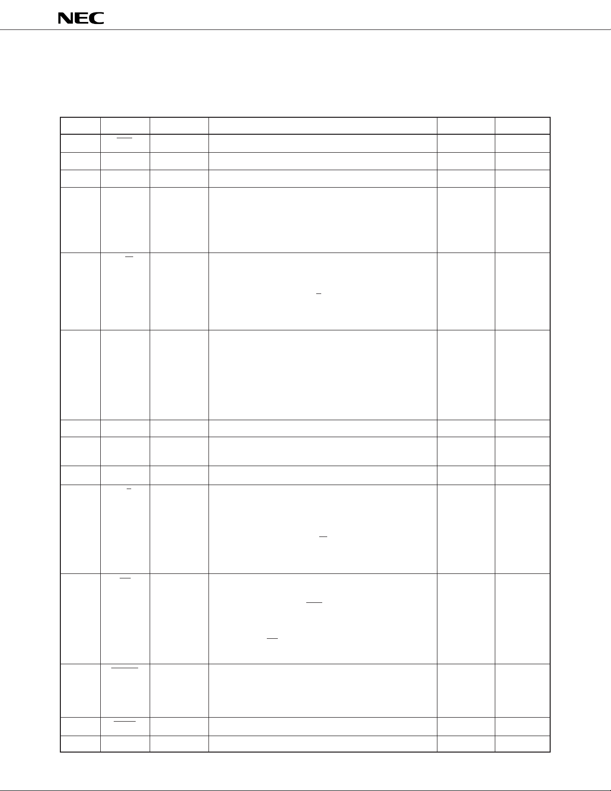
1. PIN FUNCTIONS
1.1 List of Pin Functions
Pin No. Pin Name Input/Output Function I/O Format At Reset
1 SCK Input Input for serial clock used to interface with microcontroller. CMOS input Input
2 SI Input Input for serial data used to interface with microcontroller. CMOS input Input
3 SO Output Output for serial data used to interface with microcontroller. CMOS output High level
4 IRQ Output Output used by interrupt request signals generated by CMOS output Low level
communication and command execution results.
Used as operation start request signal to microcontroller.
The interrupt request signal is output for 8 µs or longer
at high level.
5 R/W Input Input for switching serial interface read/write mode. CMOS input Input
When high, it is in the read mode. When low, it is in the
write mode.
When this pin is low and C/D pin high, the read and write
modes can be switched by commands input from the serial
interface.
6 XI –– Connection pins for system clock resonator. –– (Oscillation
7 XO Use a 12- or 12.58-MHz crystal, or ceramic resonator. continues)
Frequency precision depends on the communication mode
used.
Mode 0 : ±1.5 %
Mode 1 : ±1.5 %
Mode 2 : ±0.5 %
8 GND –– Ground –– ––
9 BUS– Input/output Input/output for IEBus. –– High
10 BUS+ impedance
11 AVDD ––
12 C/D Input Input used to switch between processing data input to the CMOS input Input
13 CS Input Chip select input. CMOS input Input
IEBus driver/receiver analog power supply. Connect to VDD.
serial interface as commands or data.
When set to high, data is processed as commands; when
low, data is processed as data.
When this pin is high and R/W pin low, the read and write
modes can be switched by commands input from the serial
interface.
When low, serial interface input is enabled.
When high, serial clock (SCK) input is disabled, SO pin
becomes high impedance, and the serial clock counter is
reset.
The status of CS pin is not affected by IEBus transmit and
receive operations.
–– ––
14 RESET Input System reset signal input pin. CMOS input Input
Low input effects a reset.
Always input the low signal for 6 µs or longer after turning
on the power.
15 TEST Input Always connect this pin to the VDD. CMOS input ––
16 VDD –– Positive power supply input. Apply a voltage of 5 V ±10 %. –– ––
5

µ
PD6708
2. IEBus OPERATION
2.1 Operation Overview
★
The
µ
PD6708 is an IEBus interface CMOS LSI device.
The IEBus is a bus for a small-scale digital data transfer system designed to transfer data between electronic devices.
The µPD6708 is connected to a microcontroller incorporated in electronic equipment with a serial interface (SCK, SO,
SI pins). The data and commands required to transfer data with the host controller (microcontroller) are set via this serial
interface.
µ
When the host controller transmits data to the
(BUS+ and BUS–). Data received from the BUS pins can be read by the host controller via the serial interface.
PD6708 via the serial interface, signals are output from the BUS pins
6
µ
PD6708
2.2 IEBus Communication Protocol
An overview of the IEBus is as follows.
• Communication system: Half-duplex asynchronous communication
• Multi-master system
All the units connected to the IEBus can transfer data to the other units.
• Broadcast communication function (communication between one unit and multiple units)
Group broadcast communication: Broadcast communication with group units
General broadcast communication: Broadcast communication with all units.
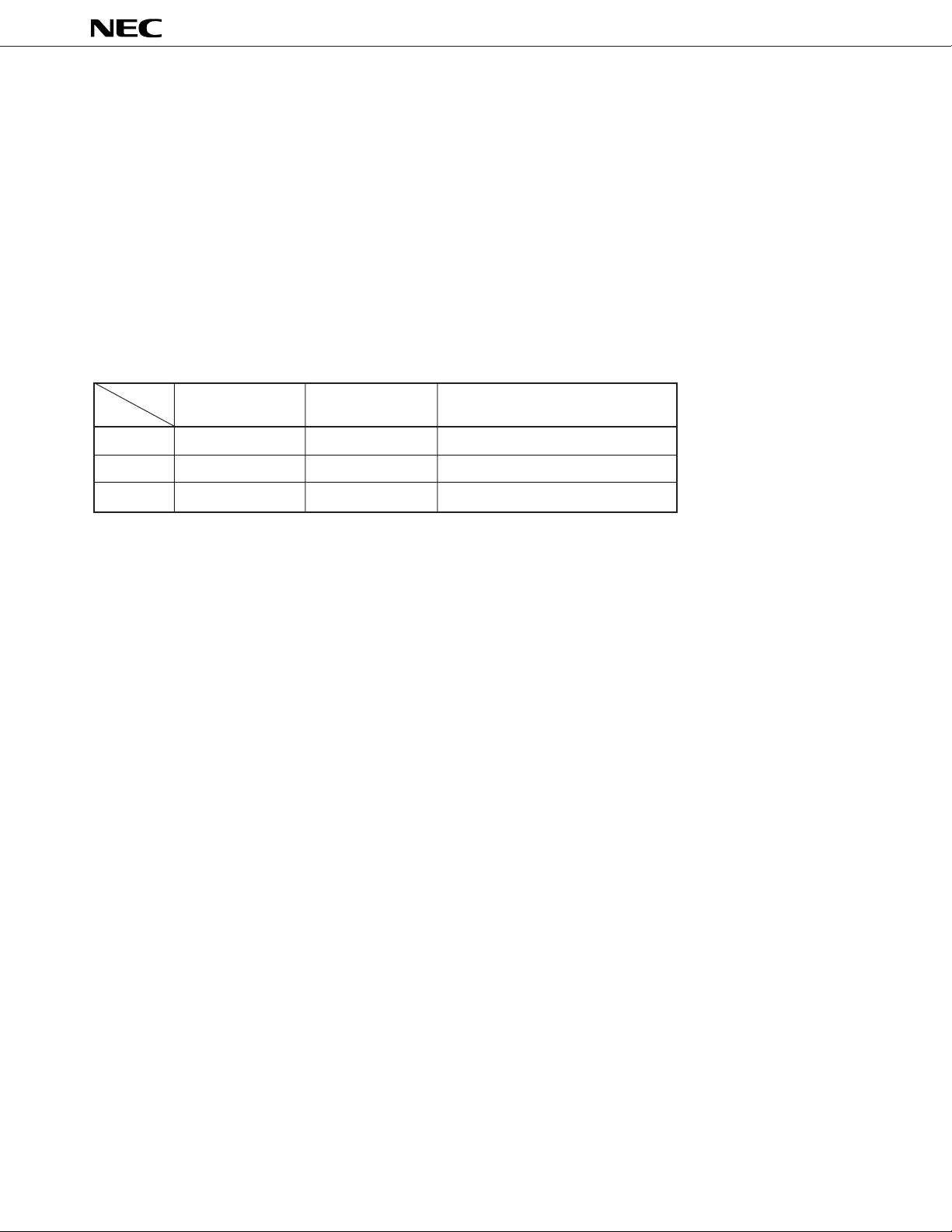
• Three modes with different transfer speeds selectable.
fX = 12 MHz fX = 12.58 MHz Maximum Number of Transfer Bytes
(bytes/frame)
Mode 0 Approx. 3.9 Kbps Approx. 4.1 Kbps 16
Mode 1 Approx. 17 Kbps Approx. 18 Kbps 32
Mode 2 Approx. 26 Kbps Approx. 27 Kbps 128
• Access control: CSMA/CD (Carrier Sense Multiple Access with Collision Detection)
The priority order for bus occupancy is as follows.
★
<1> Broadcast communication takes precedence over ordinary communication (i. e., communication between one
unit and another).
<2> The lowest master address has the highest priority.
• Communication scale
Number of units: MAX. 50
Cable length: MAX. 150 m (with twisted-pair cable <Resistance: 0.1 Ω/m or less>)
Load capacity: MAX. 8000 pF <between BUS– and BUS+>, fX = 12 MHz
MAX. 7100 pF <between BUS– and BUS+>, f
Terminating resistor: 120 Ω
X = 12.58 MHz
7
µ
PD6708
2.2.1 Bus mastership determination (arbitration)
When a unit connected to the IEBus controls another unit, it performs an operation to occupy the bus. This operation
★
is called arbitration.
Arbitration is to select one unit, and if several units begin to transmit data simultaneously, gives permission to occupy
the bus to that one unit.
So that one unit is granted the permission to occupy the bus as a result of the arbitration, the following priority conditions
are determined.
Remark The units not given permission through arbitration are automatically allowed to get into retransfer mode (number
of retransfer times for the
µ
PD6708: 3).
(1) Priority according to type of communication
Broadcast communication (between a single and multiple units) takes precedence over ordinary communication
(between single units).
(2) Priority according to master address
If the communication devices are of the same type, the unit with the lowest master address has the highest priority.
Example The master address comprises 12 bits, and unit 000H has the highest priority while unit FFFH has the lowest
priority.
2.2.2 Communication modes
The IEBus is provided with three communication modes with different transfer speeds. The transfer speed and maximum
number of transfer bytes in a single communication frame in each communication mode are shown in Table 2-1.
Table 2-1. Transfer Speed and Maximum Number of Transfer Bytes in Each Communication Mode
Communication Mode Maximum Number of Transfer Bytes (bytes/frame) Actual Transfer Speed
fX = 12 MHz
0 16 Approx. 3.9 Approx. 4.1
1 32 Approx. 17 Approx. 18
2 128 Approx. 26 Approx. 27
Note 2
Note 1
(Kbps)
fX = 12.58 MHz
Note 2
Notes 1. Actual transfer speed when the maximum number of bytes is transferred
µ
2. Oscillation frequency when the
PD6708 is used
Cautions 1. A communication mode is selected for each unit connected to the IEBus before communication is
performed. If the communication mode of the master unit is not the same as that of the unit with
which the master unit is to communicate (slave unit), communication cannot be performed correctly.
2. If the oscillation frequency of one unit is fx = 12 MHz and that of the other unit is fx = 12.58 MHz,
communication cannot be performed correctly even if the communication mode is the same. Make
sure that the oscillation frequencies of the two units to communicate are the same.
8

µ
PD6708
2.2.3 Communication address
With the IEBus, a 12-bit communication address is assigned to each unit. The communication address is made up as
follows.
Higher 4 bits: Group number (number which identifies the group to which the unit belongs)
Lower 4 bits: Unit number (number which identifies a unit within a group)
2.2.4 Broadcast communication
In ordinary communication, there is only one master unit and one slave unit, and transmission or reception is performed
on an one-to-one basis. In broadcast communication, however, there are a number of slave units and the master unit
performs transmission with these slave units. Because there are several slave units, no acknowledge signals is returned
from the slave units during communication.
Whether broadcast communication or ordinary communication is performed is specified by the broadcast bit (for the
broadcast bit, see 2.3 (1) <2> “Broadcast bit”).
There are two kinds of broadcast communication, as follows.
(1) Group broadcast communication
Broadcast communication is performed to the units in a group whose group numbers are the same as that specified by
the higher 4 bits of the communication address.
★
(2) General broadcast communication
Broadcast communication is performed to all units irrespective of their group numbers.
Group broadcast communication or general broadcast communication is identified by the value of a salve address (for
the slave address, see 2.3 (3) “Slave address field”).
9
µ
PD6708
2.3 Transfer Protocol
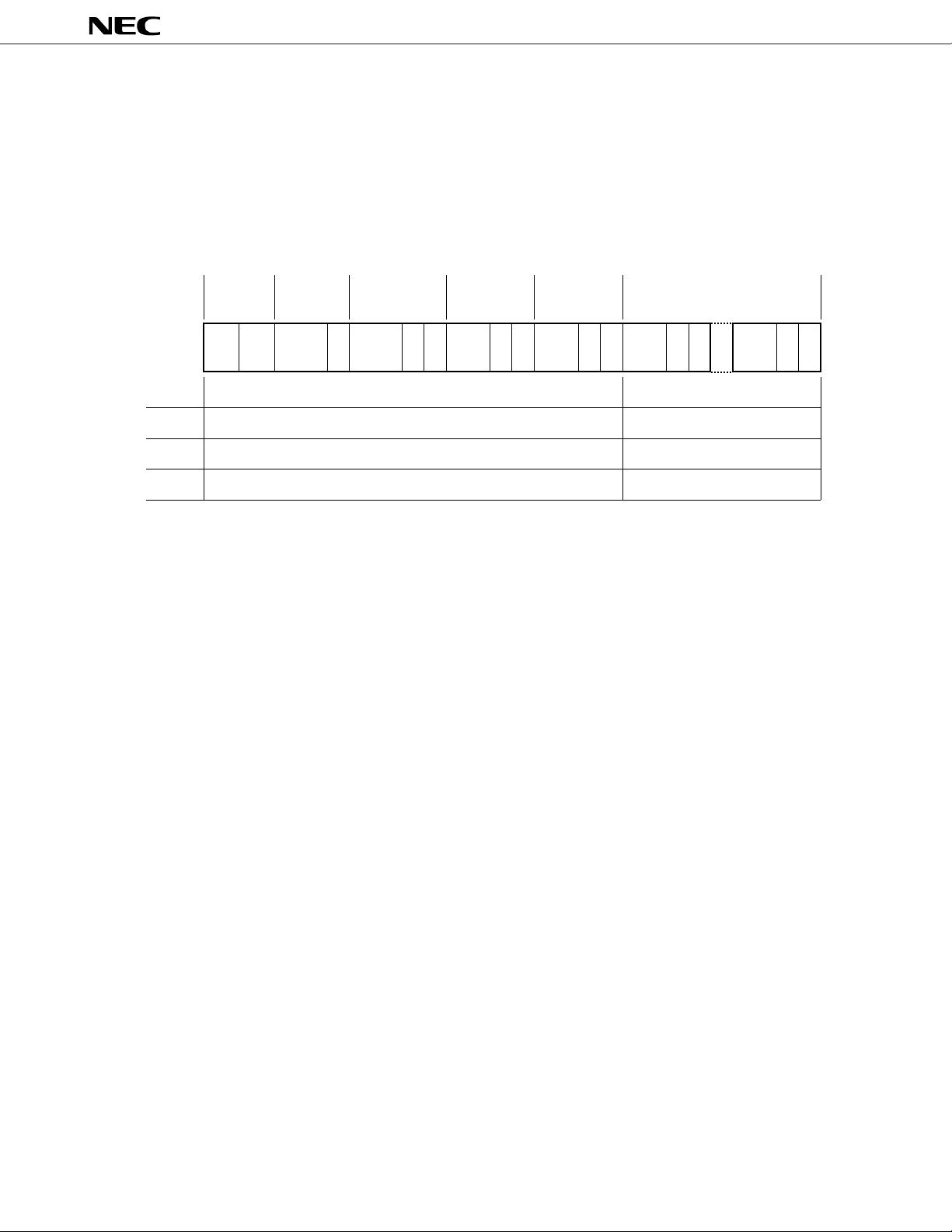
The IEBus transfer signal format is shown in Figure 2-1.
Data is transferred as a series of signals called a communication frame. The number of data that can be transferred in
one communication frame and the transfer speed differ depending on the communication mode.
Figure 2-1. Transfer Signal Format
(fx = at 12 MHz)
★
Field Name
Number of Bits
Transfer Time
Header
Start
Bit
Broad-
cast
Master
Address Field
1121 112 11411811811 811
Master
Address
Bit
Slave Address
P Slave
Address
Field
P A Control
Control Field Message
PA
Bit
Length Field
Message
Length
Bit
P A Data
Data Field
P A Data
Bit
PA
Bit
Mode 0
Mode 1
Mode 2
Approx. 7330 s
Approx. 2090 s
Approx. 1590 s
µ
µ
µ
Approx. 1590 × N s
Approx. 410 × N s
Approx. 300 × N s
µ
µ
µ
P: Parity bit (1 bit)
A: Acknowledge bit (1 bit)
When A = 0: ACK
When A = 1: NAK
N: Number of data bytes
Remark In broadcast communication, the value of the acknowledge bit is ignored.
(1) Header
A header comprises a start bit and a broadcast bit, as described below.
<1> Start bit
The start bit is a signal which tells the other units that data transmission will start.
The unit which is about to start transmitting data will output the low signal (the start bit) for a specified time, and then
outputs the broadcast bit.
If another unit is already outputting a start bit before one unit outputs a start bit, the unit will not output the start bit.
It will wait until the another unit completely outputs the start bit, and then outputs the broadcast bit.
The units other than the one that has started transmission detect this start bit and enters the reception state.
<2> Broadcast bit
The broadcast bit distinguishes between broadcast communication and ordinary communication.
When this bit is ‘0’, it indicates broadcast communication; when it is ‘1’, it indicates ordinary communication. There
are two types of broadcast communication: group broadcast and general broadcast. These types are identified by the
value of the slave address (for the slave address, see (3) “Slave address field”).
In broadcast communication, there are a number of slave units. Therefore, the acknowledge bit is not returned in the
fields described in (2) below and onward.
If two or more units start to transmit a communication frame simultaneously, broadcast communication takes
precedence over ordinary communication, and wins in the arbitration.
10

µ
PD6708
(2) Master address field
The master address field is used to transmit the unit address of the master unit (master address) to the other units.
The master address field consists of master address bits and a parity bit.
The master address comprises 12 bits and is output from the MSB.
If two or more units start transmitting the broadcast bit of the same value simultaneously, the arbitration decision is made
by the master address field.
The master address field compares the data the master has output with the data on the bus each time the master transmits
1 bit of data. If the master address output by the master unit is different from the data on the bus, the master unit assumes
that it has lost in arbitration, stops transmission, and enters the reception state.
Because the IEBus has a wired-AND configuration, the unit having the lowest master address of the units participating
in the arbitration (arbitration masters) wins in the arbitration. Ultimately, only one unit remains in the transmission state
as the master unit after outputting a 12-bit master address.
This master unit then outputs a parity bit
slave address field.
Note Even parity is used. When the number of the bits that are ‘1’ in the master address is odd, the parity bit is ‘1’.
(3) Slave address field
The slave address field is used to transmit the address (slave address) of a unit (slave unit) with which the master wishes
to communicate.
The slave address field consists of slave address bits, a parity bit, and an acknowledge bit.
The slave address comprises 12 bits and is output from the MSB. After the 12-bit slave address is transmitted, the parity
bit is output to prevent the slave address from being received incorrectly. Next, the master unit looks for the acknowledge
signal (bit) from the slave unit to confirm that the slave unit exists on the bus. When the master unit detects the acknowledge
signal, it starts outputting the control field. In the case of broadcast communication, however, the master unit outputs the
control field without waiting for the acknowledge bit.
A slave unit outputs the acknowledge signal if it has detected that its slave address coincides with that selected by the
master and that the parities of both the master and slave addresses are even. If the parity is odd, the slave unit assumes
that the master or slave address has not been correctly received, and does not output the acknowledge signal. In this case,
the master unit enters the standby (monitor) state and communication ceases.
In the case of broadcast communication, the slave address is used to distinguish between group broadcast and general
broadcast as follows:
Note
, makes the other units confirm the master address, and then outputs the
★
Slave address = FFFH: General broadcast communication
Slave address ≠ FFFH: Group broadcast communication
Remark In the case of group broadcast communication, the group number is the value of higher 4 bits of the slave
address.
11

µ
PD6708
(4) Control field
★
The control field indicates the type of data and the transfer direction of the subsequent data field.
The control field consists of 4 control bits, a parity bit, and an acknowledge bit.
The control bits are output from the MSB.
A parity bit is output after the control bits. When the parity is even and the slave can execute the function requested
by the master unit, the slave unit outputs an acknowledge signal, and then outputs the next message length field. If the
slave unit cannot execute the function requested by the master unit even if the parity is even, or if the parity is odd, the slave
unit does not output the acknowledge signal but returns to the standby (monitor) state.
After the master unit has confirmed the acknowledge signal, it starts outputting the next message length field.
If the master unit is cannot confirm the acknowledge signal, it enters the standby state and stops communication. In
the case of broadcast communication, however, the master unit starts outputting the message length field without confirming
the acknowledge signal.
For the functions of the control bits, see Table 2-3.
(5) Message length field
The message length field is used to specify the number of communication data bytes.
The message length field comprises 8 message length bits, a parity bit and, an acknowledge bit.
The message length bits are output from the MSB. The message length bits indicate the number of communication data
bytes as shown in Table 2-2.
Table 2-2. Meaning of Message Length Bits
Message Length Bits (hex) Number of Transmission Data Bytes
01H 1 byte
02H 2 bytes
::
::
FFH 255 bytes
00H 256 bytes
Remark In the communication mode, if the number of bytes exceeding the maximum number of transfer bytes per frame
is set, two or more frames are communicated. In this case, the message length bits indicate the number of
remaining communication data bytes during the second communication and onward.
The operation of this field differs depending on whether the master transmits (bit 3 of control bits is 1) or receives (bit
3 of control bits is 0) data.
<1> When master transmits data
The message length bits and parity bit are output by the master unit. The slave unit outputs the acknowledge signal
and then the next data field if it detects that the parity is even. The slave unit does not output the acknowledge signal
in the case of broadcast communication.
If the parity is odd, the slave unit assumes that the message length bits have not been received correctly, and returns
to the standby (monitor) state without outputting the acknowledge signal. In this case, the master unit also returns to
the standby state, and communication ceases.
12

µ
PD6708
<2> When master receives data
The message length bits and parity bit are output by the slave unit. The master unit outputs the acknowledge signal
if it detects that the parity bit is even.
If the parity is odd, the master unit assumes that the message length bits have not been received correctly, and returns
to the standby state without outputting the acknowledge signal. In this case, the slave unit also returns to the standby
state, and communication ceases.
(6) Data field
The data field is used to transmit/receive data to/from the slave units.
The master unit uses the data field to transmit data to and receive data from the slave units.
The data field consists of 8 data bits, a parity bit, and an acknowledge bit.
The data bits are output from the MSB.
Following the data bits, the parity bit and acknowledge bit are output from the master unit and the slave unit, respectively.
Broadcast communication is performed when only the master unit transmits data. At this time, the acknowledge signal
is ignored.
The operation differs depending on whether the master performs transmission or reception, as follows.
<1> When master transmits data
When the master unit writes data to the slave unit, the master unit transmits data bits and a parity bit to the slave unit.
The slave unit receives the data bits and parity bit. If the parity is even and the receive buffer is empty, the slave unit
outputs the acknowledge signal. If the parity is odd and the receive buffer is not empty, the slave unit denies
acknowledgment of the corresponding data and does not output the acknowledge signal.
If no acknowledge signal is output from the slave unit, the master unit transmits the same data again. The master
unit continues this operation until it detects the acknowledge signal from the slave unit or the data reaches the maximum
number of transfer bytes.
If the parity is even and the acknowledge signal has been output from the slave unit, and if the master unit has more
data to transmit and the maximum number of transfer bytes is not exceeded, the master unit will transmit the next data.
In the case of broadcast communication, the slave unit does not output the acknowledge signal, and the master unit
transfers data on a byte-by-byte basis.
★
<2> When master receives data
When the master unit reads data from the slave unit, the master unit outputs synchronization signals corresponding
to all the read bits.
The slave unit outputs the contents of the data and parity bits onto the bus in accordance with the synchronization
signals from the master unit.
The master unit reads the data and parity bit output by the slave unit, and checks the parity.
If the parity is odd or the receive buffer is not empty, the master unit denies acknowledgement of that data and does
not output the acknowledge signal. If the data is within the maximum number of transfer bytes that can be transmitted
in one frame, the master unit repeatedly reads the same data.
If the parity is even and the receive buffer is empty, the master unit acknowledges the data and transmits back the
acknowledge signal. If the data is within the maximum number of bytes that can be transmitted in one frame, the master
unit reads the next data.
★
13

µ
PD6708
(7) Parity bits
Parity bits are used to check that there is no error in the transfer data.
A parity bit is added to the master address bits, slave address bits, control bits, message length bits, and data bits.
Even parity is used. If the number of the bits that are ‘1’ bits in data is odd, the parity bit is ‘1’, and if the number of the
bits that are ‘1’ bits is even, the parity bit is ‘0’.
(8) Acknowledge bits
In ordinary communication (between two units), an acknowledge bit is added to the following places to confirm that data
has been acknowledged correctly.
• At the end of the slave address field.
• At the end of the control field.
• At the end of the message length field.
• At the end of a data field.
The definition of the acknowledge bit is as follows.
• ‘0’: Indicates that transfer data has been acknowledged (ACK).
• ‘1’: Indicates that transfer data has not been acknowledged (NAK).
Note that the value of the acknowledge bit is ignored in broadcast communication.
<1> Acknowledge bit at the end of the slave field
When any of the following conditions is met, the acknowledge bit at the end of the slave field is NAK, and
communication is discontinued.
• If the parity of the master address bits or slave address bits is incorrect.
• If a timing error (error in bit format) occurs.
• If the slave unit does not exist.
<2> Acknowledge bit at the end of the control field
When any of the following conditions is met, the acknowledge bit at the end of the control field is NAK, and
communication is discontinued.
• If the parity of the control bits is incorrect.
★
• If bit 3 of the control bits is ‘1’ (write operation) when the slave receive buffer
• If the control bits indicate read operation (3H or 7H) when the slave transmit buffer
• If 3H, 6H, 7H, AH, BH, EH, or FH of control bits is requested from a unit other than the unit which set the lock when
a lock has been set.
• If the control bits indicate lock address read (4H) when a lock has not been set.
• If a timing error occurs.
• If the control bits are undefined.
Note
is not empty.
Note
is empty.
Note See 2.4 (1) “Reading slave status (SSR) (control bit: 0H, 6H)”.
14

µ
PD6708
<3> Acknowledge bit at the end of a message length field
When either of the following conditions is met, the acknowledge bit at the end of the message length field is NAK,
and communication is discontinued.
• If the parity of the message length bits is incorrect.
• If a timing error occurs.
<4> Acknowledge bit at the end of a data field
When any of the following conditions is met, the acknowledge bit at the end of a data field is NAK, and communication
is discontinued.
• If the parity of the data bits is incorrect
• If a timing error occurred in or after the previous acknowledge bit transmission.
• If the receive buffer is full and cannot accept any more data
Note In this case, if the number of transfer bytes is within the maximum number of bytes which can be transmitted, the
transmitting side re-executes transmission of that data field.
Note
.
Note
.
15
2.4 Transfer Data (Contents of Data Field)
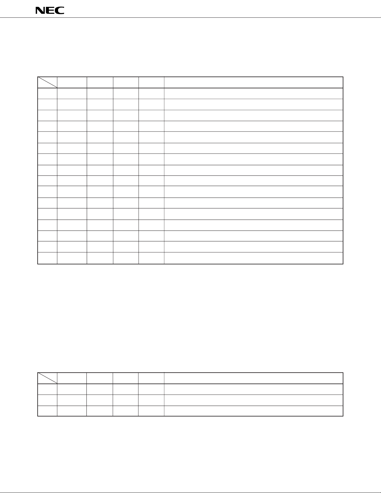
The contents of the data field are data specified by the control bits.
Table 2-3. Functions of Control Bits
µ
PD6708
Note 1
★
Bit 3
0H 0 0 0 0 Reads slave status (SSR)
1H 0 0 0 1 Undefined
2H 0 0 1 0 Undefined
3H 0 0 1 1 Reads and locks data
4H 0 1 0 0 Reads lock address (lower 8 bits)
5H 0 1 0 1 Reads lock address (higher 4 bits)
6H 0 1 1 0 Reads and unlocks slave status (SSR)
7H 0 1 1 1 Reads data
8H 1 0 0 0 Undefined
9H 1 0 0 1 Undefined
AH 1 0 1 0 Writes and locks command
BH 1 0 1 1 Writes and locks data
CH 1 1 0 0 Undefined
DH 1 1 0 1 Undefined
EH 1 1 1 0 Writes command
FH 1 1 1 1 Writes data
Bit 2 Bit 1 Bit 0 Function
Note 2
Notes 1. Depending on the value of bit 3 (MSB), the transfer direction of the message length bits of the subsequent
message field and data field differs.
When bit 3 is “1”, data are transferred from the master unit to the slave unit.
When bit 3 is “1”, data are transferred from the slave unit to the master unit.
2. 3H, 6H, AH, and BH are control bits that specify locking or unlocking.
If any of undefined values 1H, 2H, 8H, 9H, CH, or DH is transmitted, no acknowledge bit is returned.
A unit locked by the master unit rejects acknowledging the control bits and does not output the acknowledge bit if the
control bits received from the master unit which requested locking is in any other state than that shown in Table 2-4.
Table 2-4. Control Field Corresponding to Locked Slave Unit
Bit 3 Bit 2 Bit 1 Bit 0 Function
0H 0 0 0 0 Reads slave status
4H 0 1 0 0 Reads lock address (lower 8 bits)
5H 0 1 0 1 Reads lock address (higher 4 bits)
16
µ
PD6708
(1) Reading slave status (SSR) (control bit: 0H, 6H)
The master unit can learn the reason why the slave unit has not returned the acknowledge bit (ACK) by reading the
slave status.
The slave status is determined by the results of the last communication performed by the slave unit.
All the slave units can provide slave status information.
The meanings of the slave status are shown in Table 2-5.
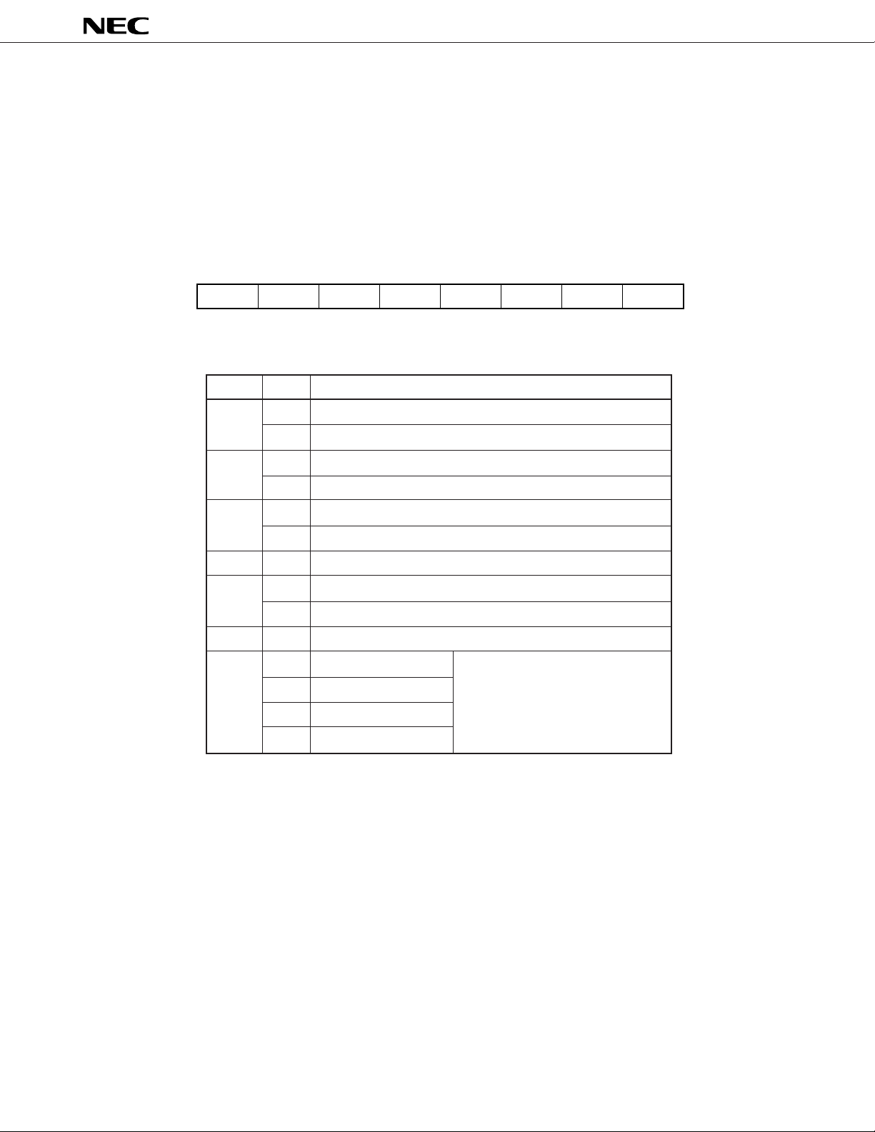
Figure 2-2. Bit Configuration of Slave Status (SSR)
MSB LSB
Bit 7 Bit 6 Bit 5 Bit 4 Bit 3 Bit 2 Bit 1 Bit 0
Table 2-5. Meanings of Slave Status
Bit Value Meaning
Note 1
Bit 0
Note 2
Bit 1
Bit 2 0 Unit is not locked.
Bit 3 0 Fixed to ‘0’
Note 3
Bit 4
Bit 5 0 Fixed to ‘0’
0 Slave transmit buffer empty
1 Slave transmit buffer is not empty.
0 Slave receive buffer empty
1 Slave receive buffer is not empty.
1 Unit is locked.
0 Slave transmission ends
1 Slave transmission enabled
★
Bit 7 00 Mode 0 Indicates the highest mode the unit
Bit 6 01 Mode 1 supports
10 Mode 2
11 For future expansion
Note 4
.
Notes 1. The slave transmit buffer is the buffer accessed during data read processing (control bits: 3H, 7H).
µ
With the
PD6708, this buffer corresponds to the write data buffer (WDB) when the SETSD command is valid
(see 5.2.6 “SETSD command”).
2. The slave receive buffer is the buffer accessed during data write processing (control bits: 8H, AH, BH, EH, FH).
With the
µ
PD6708, this buffer corresponds to the read data buffer (RDB).
3. The value of bit 4 can be selected by INIT command (see 5.2.1 “INIT command”).
4. Because the µPD6708 can support mode 2, bits 7 and 6 are fixed at ‘10’.
17

µ
PD6708
(2) Transferring data command (control bit: read (3H, 7H), write (AH, BH, EH, FH))
During data read (3H, 7H), the data in the data buffer of the slave unit are read to the master unit.
During data write (BH, FH) or during command write (AH, EH), the data the slave unit has received are processed
according to the operation convention.
Remarks 1. The user can voluntarily select data and command as his system requires.
2. Control bits 3H, AH, and BH may be locked depending on the communication condition and status.
(3) Reading lock address (control bits: 4H, 5H)
★
When the lock address is read processing (4H, 5H), the address (12 bits) of the master unit that has issued the lock
instruction is read in 1-byte units, as shown below.
Figure 2-3. Lock Address Configuration
MSB LSB
Control Bits : 4H
Control Bits : 5H
(4) Locking and unlocking (locking (3H, AH, BH), unlocking (6H))
The lock function is used to transfer a message over two or more frames.
A locked unit receives data only from the unit that has locked the unit.
Locking and unlocking are performed as described below.
<1> Locking
After the transmission/reception of the acknowledge bit ‘0’ of the message length field by the control bits (3H, AH,
BH) which specify the lock has ended, if the communication frame is completed without completing the transmission or
reception of the number of data bytes specified by the message length bits, the slave unit is locked by the master unit.
At this time, the bit (bit 2) relating to the locking of the byte which indicates the slave status is set to ‘1’.
<2> Unlocking
After completion of transmission or reception of data in one frame by the number of data bytes specified by the message
length bits with control bits (3H, AH, or BH) specifying locking or control bits (6H) specifying unlocking, the slave unit
is unlocked by the master unit. At this time, the bit (bit 2) relating to the locking of the byte which indicates the slave
status is reset to ‘0’.
Lower 8 Bits
Undefined Higher 4 Bits
Locking and unlocking are not performed in the case of broadcast communication.
Caution To unlock the unit specified to be unlocked by the unit itself, the INIT command (see 5.2.1 “INIT
µ
command”) must be executed with the
the GETSA command (see 5.2.7 “GETSA command”).
18
PD6708 (Whether a unit is locked or not can be checked by using
2.5 Bit Format
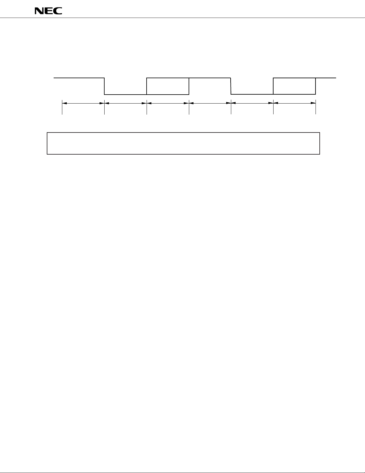
The IEBus communication frame bit format (concept) is shown in Figure 2-4.
Figure 2-4. IEBus Bit Format (Concept)
Logic "1"
Logic "0"
µ
PD6708
★
Preparation Period
Logic “1”: Potential difference between bus lines (BUS+ pin and BUS– pin) is 20 mV or lower (low level).
Logic “0”: Potential difference between bus lines (BUS+ pin and BUS– pin) is 120 mV or higher (high level).
Preparation period: The first or subsequent low-level (logic “1”) period
Synchronous period: The next high-level (logic “0”) period
Data period: The period that expresses the bit value (logic “1”: low level; logic “0”: high level)
The synchronous period and data period have approximately the same length.
The IEBus uses bit-by-bit synchronization. The specifications for the total bit time and the periods allocated to the bits
depend on the type of transfer bit, and on whether the unit is the master unit or the slave unit.
Synchronous Period
Data Period
Preparation Period
Synchronous Period
Data Period
19
3. INTERNAL CONFIGURATION
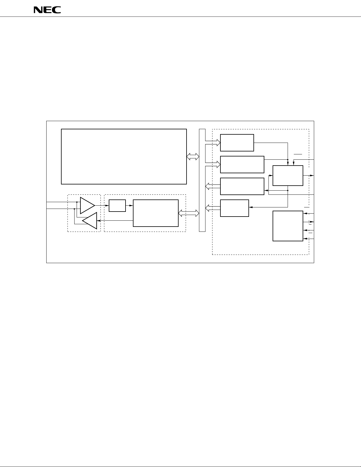
The µPD6708 is composed of the following four blocks.
(1) Data link layer controller
(2) Physical layer controller
(3) IEBus driver/receiver
(4) Host interface
Figure 3-1. µPD6708 Internal Blocks
Status Register
(STR)
Host Interface
µ
PD6708
BUS+
BUS–
IEBus Driver/Receiver
Receiver
Driver
Data Link Layer Controller
Filter
Bit Sequencer
Physical Layer Controller
Read Data Buffer
(RDB) 20 Bytes
Write Data Buffer
(WDB) 4 Bytes
Command Register
(CMR)
Shift
Register
Serial I/O
Controller
SCK
SO
SI
CS
IRQ
C/D
R/W
20
µ
PD6708
3.1 Data Link Layer Controller
The data link layer controller performs processing of the IEBus protocol data link layer (frame composition and resolution,
communication error detection, etc.), execution of communication control commands set by the host controller, and generate
a return code that informs the host controller of the communication status.
3.2 Physical Layer Controller
The physical controller performs generation and resolution of bit timing and also converts the signals between the bus
lines through the driver/receiver.
3.3 IEBus Driver/Receiver
The driver/receiver performs conversion between the logic signals within the µPD6708 and the IEBus signals. The IEBus
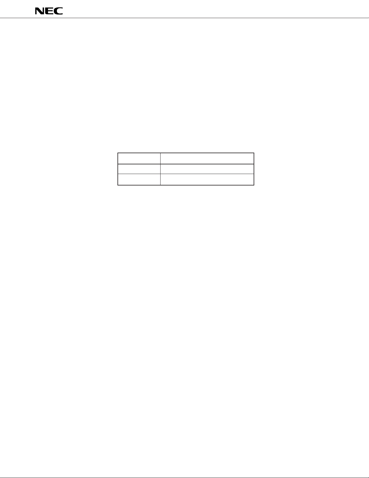
signals and their relationship to the logic statuses are shown in Table 3-1.
Table 3-1. Relationship between IEBus Signals and Logical Statuses
Logical Status IEBus Signals
0 (BUS+) – (BUS–) ≥ 120mV
1 (BUS+) – (BUS–) ≤ 20mV
3.4 Host Interface
The host Interface is a block which controls the transmission and reception of data to and from the host controller. It
accepts communication control commands, passes on return codes, and forwards transmit data.
The forwarding of transmit data takes place through the FIFO buffers, 4 bytes of write data buffer (WDB) and 20 bytes
of read data buffer (RDB). It also absorbs the differences between IEBus transmission speed and the transmission speed
on the serial interface between the
µ
PD6708 and the host controller.
21
µ
PD6708
4. INTERFACING WITH HOST CONTROLLER
This chapter will explain the interfacing that occurs between the µPD6708 and the host controller.
4.1 Accessible Buffers and Registers from Host Controller
The host controller, which controls the µPD6708, can access the write data (WDB), the read data buffer (RDB), the
command register (CMR), and the status register (STR) within the
4.1.1 Write data buffer (WDB)
WDB is a 4-byte FIFO buffer in which the host controller transmit data and the parameters of the communication control
commands are written.
4.1.2 Read data buffer (RDB)
RDB is a 20-byte FIFO buffer which stores the receive data acknowledged by the data link layer controller in the
The host controller reads the
µ
PD6708 receive data from RDB.
4.1.3 Command register (CMR)
CMR is an 8-bit register used to write control commands for the µPD6708.
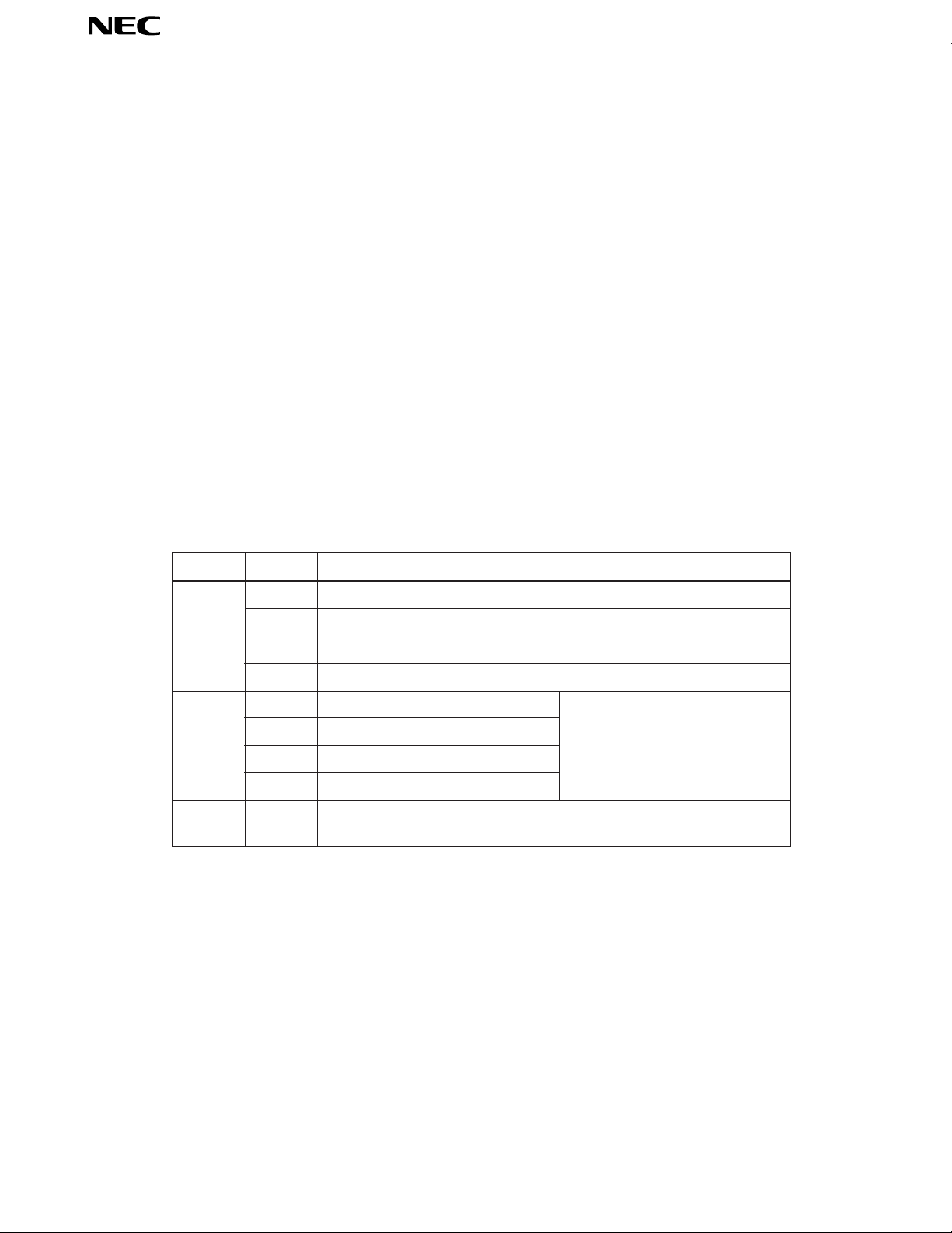
As shown in Table 4-1, the host controller sets the reset mode and the host interface mode in higher 4 bits and sets the
communication control command code in lower 4 bits.
µ
PD6708.
µ
PD6708.
Table 4-1. Contents of Command Register
Bit Value Meaning
Bit 7 1 Entering the reset mode
0 Exiting the reset mode
Bit 6 1 Data of lower 4 bits of CMR is valid.
0 Data of lower 4 bits of CMR is not valid.
Bit 5 00 Change of mode through pin control Switches the host interface mode
Bit 4 01 Data write mode
10 Data read mode
11 Status read mode
Bit 3 to Set the communication control command codes
Bit 0
22
 Loading...