NEC UPD6467GR Datasheet
DATA SHEET
MOS INTEGRATED CIRCUIT
µ
PD6467
ON-SCREEN CHARACTER DISPLAY CMOS IC FOR 512-CHARACTER,
12-ROW, 28-COLUMN, CAMERA-CONTAINED VCR
The µPD6467 is a CMOS LSI for on-screen character display, and can be used in combination with a microcomputer
to display the tape counter, time, and date in the view finder of a video camera, or the time of a video tape, messages
such as dates on pictures, and channel number on a TV screen.
Characters are displayed in 12 (horizontal) by 18 (vertical) dots. Two or more characters can be combined to display
Kanji (Japanese characters) and symbols. This LSI supports color view finders and is provided with three sets of
character output signals (RGB output: for color view finder, V
monitor pin (or recording)).
In addition, the µPD6467 is also equipped with a power-ON clear function and a video RAM batch clear command
so that it can mitigate the workload of the microcomputer.
The command format of this LSI is identical to that of the existing models, the µPD6461, 6462 and 6466, and
µ
therefore, the
can be used.
PD6467 is compatible with the existing models, and the software resources for the existing models
C1 output: for recording (or monitor pin), VC2 output: for
FEATURES
• Number of display characters : 12 rows, 28 columns (336 characters)
• Types of character : 512 types (ROM). Changeable by using mask code option.
• Character size : Can be expanded up to four-fold in vertical and horizontal directions
independently, in units of lines.
• Number of character colors : 8 colors
• Framing : Framing or no framing, or white or black framing selectable in screen units.
• Dot matrix : 12 (horizontal) × 18 (vertical) dot configuration. No gap between adjacent
characters.
• Blinking : Blinking can be turned ON/OFF in character units. The blinking ratio is 1:1.
The blinking frequency can be selected from about 1 Hz, about 2 Hz, and
about 0.5 Hz in screen unit.
• Character color reversing function : The color of the character and that of the background can be reversed.
• Character left and right reverse : Left and right can be reversed for display in character units.
• Background : No background, blank background, or filled background selectable in screen
units.
• Blue back function : Blue or white can be selected as the background.
• External dot clock input : Frequency 2-divide function is selectable.
• Signal output : 3 sets (output (1) R, G, B + BLK/V
R
BLK/B + BBLK/G + GBLK selectable by command)
When output (1) is selected, V
types.
• Video RAM data clear : Implemented by video RAM batch clear command or by clear function on
power-ON.
C1 + VBLK1/VC2 + VBLK2 and output (2) R +
C1 and VC2 outputs can be selected from three
The information in this document is subject to change without notice. Before using this document, please
confirm that this is the latest version.
Not all devices/types available in every country. Please check with local NEC representative for availability
and additional information.
Document No. S14455EJ1V0DS00 (1st edition)
Date Published November 1999 N CP(K)
Printed in Japan
©
1999

µ
PD6467
• Interface with microcomputer : 8-bit variable word length serial input (LSB first/MSB first selectable by
command)
• Supply voltage : Supports low voltage (2.0 to 3.6 V)
• Process : CMOS low power consumption
• Small package size : 20-pin plastic shrink SOP (225 mil)
ORDERING INFORMATION
Part Number Package
µ
PD6467GR-xxx 20-pin plastic shrink SOP (225 mil)
µ
Remarks 1. NEC’s standard model is the
For the details of the character generator ROM, refer to 5. CHARACTER PATTERNS.
2. xxx indicates a ROM code suffix.
PD6467GR-001.
2
Data Sheet S14455EJ1V0DS00
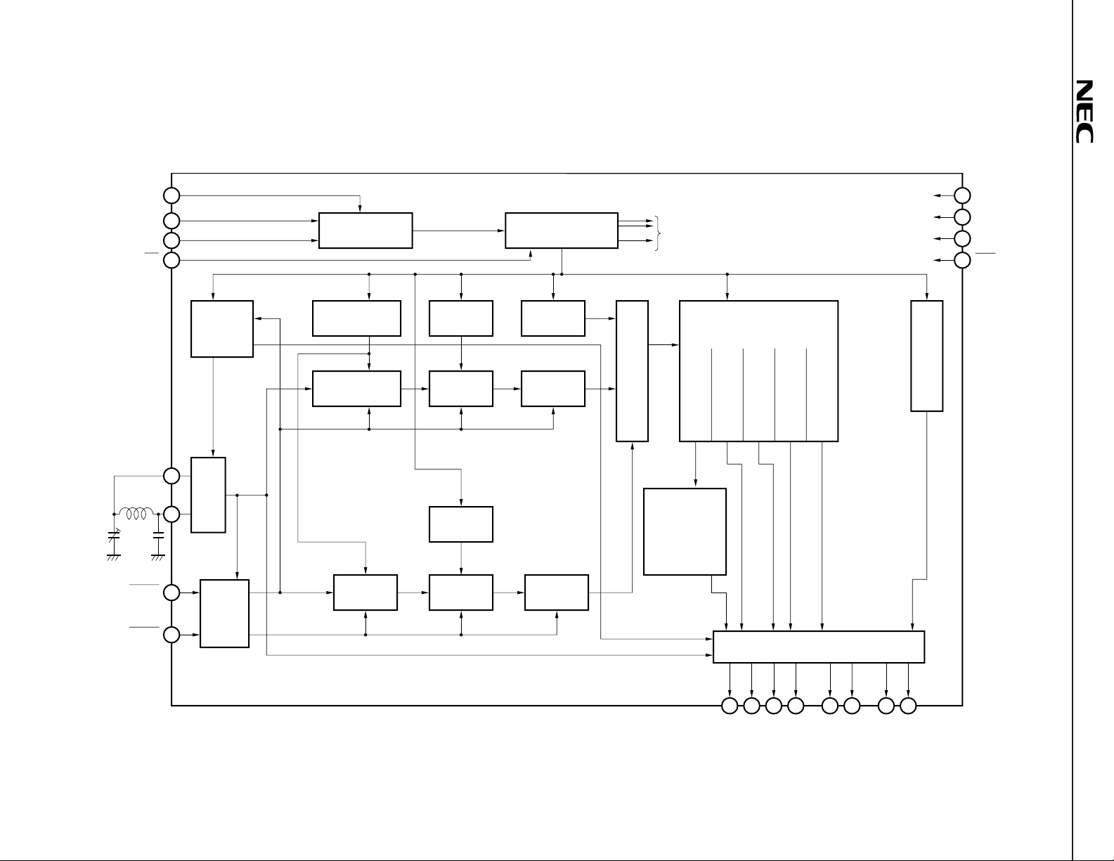
BLOCK DIAGRAM
CMDCT
Data input shift
register
DATA
CLK
CS
Instruction decoder
Data selector
...
Control signals
Display
control
register
Character size
register
Horizontal
address
register
Write
address
counter
Horizontal size
counter
Horizontal
position
counter
Horizontal
address
counter
Vertical
address
register
Oscillation
circuit
Synchronization
protection
circuit
TEST
V
DD
GND
PCL
Character
data
9 bits
×
336 words
Color
data
3 bits
×
336 words
Blink
data
1 bit
×
336 words
Reverse
data
1 bit
×
336 words
Output
specification
data 1 bit
×
336 words
Video RAM
Background
control
data
register
Hsync
Vsync
Vertical
position
counter
Vertical size
counter
Output controller
V
R
V
BLK
V
B
V
G
BLK2V
C2
BLK1V
C1
(G
BLK
)
(R
BLK
)
(B
BLK
)
Character
generator
ROM
12×18 bits
×
512 words
OSC
IN
OSC
OUT
Vertical
address
counter
9
5
10
4
6
3
1
2
8
7
20
19
16 17 18 15 12 11
14
13
Data Sheet S14455EJ1V0DS00
3
Remark Signals in ( ) are set by using an initial status setting command (RGB + RGB compatible blanking).
µ
PD6467
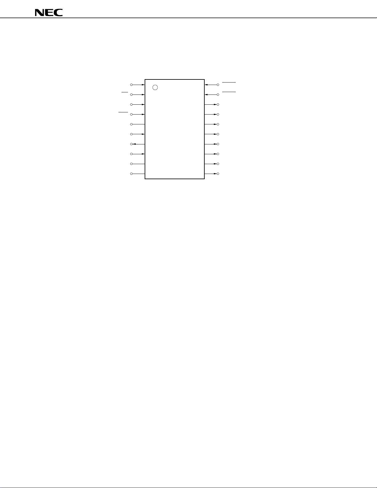
PIN CONFIGURATION (Top View)
20-pin plastic shrink SOP (225 mil)
µ
PD6467GR-xxx
µ
PD6467
CLK 1
CS 2
DATA 3
PCL 4
DD
V
5
CMDCT 6
OSC
OSC
OUT
IN
7
8
TEST 9
GND 10
Remarks 1. xxx indicates a ROM code suffix.
2. Signals in ( ) are set by using an initial status setting command (RGB + RGB compatible blanking).
20
19
18
17
16
15
14
13
12
11
Hsync
Vsync
V
B
V
G
V
R
V
BLK
(B
VC2 (G
BLK2 (R
V
C1
BLK1
BLK
BLK
BLK
)
)
)
4
Data Sheet S14455EJ1V0DS00

BBLK : Blanking B
BLK1, BLK2 : Blanking Output 1, 2
CLK : Clock
CMDCT : Command Control
CS : Chip Select
DATA : Data Input
BLK : Blanking G
G
GND : Ground
Hsync : Horizontal Synchronous Signal Input
IN : Oscillator Input
OSC
OSCOUT : Oscillator Output
PCL : Power-ON Clear
BLK : Blanking R
R
TEST : Test
B : Character Signal Output
V
VBLK : Blanking Signal Output for VR, VG, VB
VC1, VC2 : Character Signal Output 1, 2
DD : Power Supply
V
VG : Character Signal Output
VR : Character Signal Output
Vsync : Vertical Synchronous Signal Input
µ
PD6467
Data Sheet S14455EJ1V0DS00
5

PIN FUNCTIONS
Pin No. Pin Pin Name
1 CLK Clock input This pin inputs a clock for reading data. Data input to the DATA pin
2 CS Chip select input Serial transfer can be accepted if this pin is made low.
3 DATA Serial data input This pin inputs control data. Data is read in synchronization with the
4 PCL Power-ON clear This pin, when high, initializes the internal circuitry of the IC on power
5VDD Power supply This pin supplies power.
6 CMDCT Command specification This pin selects whether a command is input with the LSB first or MSB
7 OSCOUT LC oscillation I/O These are an input and an output pin for an oscillation circuit that
8 OSCIN (OSCIN: external clock generates a dot clock.
9 TEST Test pin This pin is used to test the IC. Normally, connect this pin to GND.
10 GND Ground pin Connect this pin to GND of the system.
11 BLK1 Blanking signal output 1 This pin outputs a blanking signal to cut the video signal.
12 VC1 Character signal output 1 This pin outputs a character signal, and is high-active.
13 BLK2 Blanking signal output 2 This pin outputs a blanking signal to cut the video signal. It supports
14 VC2 Character signal output 2 This pin outputs a character signal, and is high-active.
15 VBLK Blanking signal output This pin outputs a blanking signal to cut the video signal. It supports
16 VR Character signal output This pin outputs a character signal, and is high-active.
17 VG
18 VB
19 Vsync Vertical sync signal input This pin inputs a vertical sync signal. Input a negative sync signal.
20 Hsync Horizontal sync signal input This pin inputs a horizontal sync signal. Input a negative sync signal.
Note
Symbol
select first.
input) A coil and capacitor for oscillation are connected to these pins. (If
(RBLK) (blanking R) output of VC2, and is high-active.
(GBLK) (blanking G) (This pin outputs a blanking signal supporting output of VG and is
(BBLK) (blanking B) output of VR, VG, and VB, and is high-active (this pin outputs a blanking
Note
Function
is read at the rising edge of this clock.
clock input to the CLK pin.
application.
When this pin is low, the command is input with the LSB first; when
it is high, the command is input with the MSB first. To input the
command with the LSB first, this pin may be opened.
the input of an external clock is selected by the initial status setting
command, an external clock (clock synchronized with Hsync) is input.
OSCOUT is opened at this time.)
When the TEST pin is connected to GND, the test mode is not set.
It supports output of VC1, and is high-active.
(If RGB compatible blanking is selected by a command, this pin
outputs the logical sum of RBLK, GBLK, and BBLK.)
(If RGB compatible blanking is selected by a command, this pin
outputs the logical sum of VR, VG, and VB.)
(This pin outputs a blanking signal supporting output of VR and is
high-active.)
high-active.)
signal supporting output of VB and is high-active).
µ
PD6467
Note Signals in ( ) are set by the initial status setting command (RGB + RGB compatible blanking).
6
Data Sheet S14455EJ1V0DS00

µ
PD6467
CONTENTS
1. INITIAL STATUS SETTING .................................................................................................................9
1.1 Initial Status Setting .................................................................................................................9
1.2 Application Block Diagram....................................................................................................11
1.3 Display with RGB + VC1 + VC2 Pins ........................................................................................12
1.3.1 Character signal output with output select option A ..................................................................... 1 5
1.3.2 Character signal output with output select option B ..................................................................... 16
1.3.3 Character signal output with output select option C..................................................................... 1 7
1.3.4 Displaying characters specified by V
C2 ......................................................................................... 18
2. COMMAND .........................................................................................................................................19
2.1 Command Format ................................................................................................................... 19
2.2 Command List .........................................................................................................................19
2.3 Power-ON Clear Function ...................................................................................................... 21
3. DETAILS OF COMMANDS ................................................................................................................22
3.1 Video RAM Batch Clear Command .......................................................................................22
3.2 Display Control Command .................................................................................................... 2 3
3.3 Background Color/Frame Color Control Command .......................................................... 26
3.4 3-Channel Independent Display ON/OFF Command ..........................................................27
3.5 Character Color Reverse ON/OFF Command .....................................................................28
3.6 Blue Back ON/OFF Command...............................................................................................30
3.7 Character Address Bank Select Command .........................................................................31
3.8 Output Switch Control Command ........................................................................................32
3.9 Character Display Position Control Command ..................................................................34
3.10 Write Address Control Command .........................................................................................3 6
3.11 Output Pin Control Command...............................................................................................37
3.12 Character Size Control Command........................................................................................3 8
3.13 3-Channel Background Control Command .........................................................................39
3.14 Initial Status Setting Command ............................................................................................ 4 3
3.15 Display Character Control Command ..................................................................................44
3.16 Test Mode .................................................................................................................................47
4. TRANSFERRING COMMANDS ........................................................................................................4 8
4.1 1-Byte Command .....................................................................................................................48
4.2 2-Byte Command .....................................................................................................................48
4.3 2-Byte Successive Commands .............................................................................................49
4.4 Successive Input of Command.............................................................................................50
4.4.1 When 2-byte successive command end code is not used ........................................................... 50
4.4.2 When 2-byte successive command end code is used ................................................................. 50
5. CHARACTER PATTERNS.................................................................................................................51
6. ELECTRICAL CHARACTERISTICS .................................................................................................59
7. APPLICATION CIRCUIT EXAMPLE .................................................................................................64
Data Sheet S14455EJ1V0DS00
7

µ
PD6467
8. PACKAGE DRAWING........................................................................................................................65
9. RECOMMENDED SOLDERING CONDITIONS................................................................................66
8
Data Sheet S14455EJ1V0DS00
1. INITIAL STATUS SETTING
1.1 Initial Status Setting
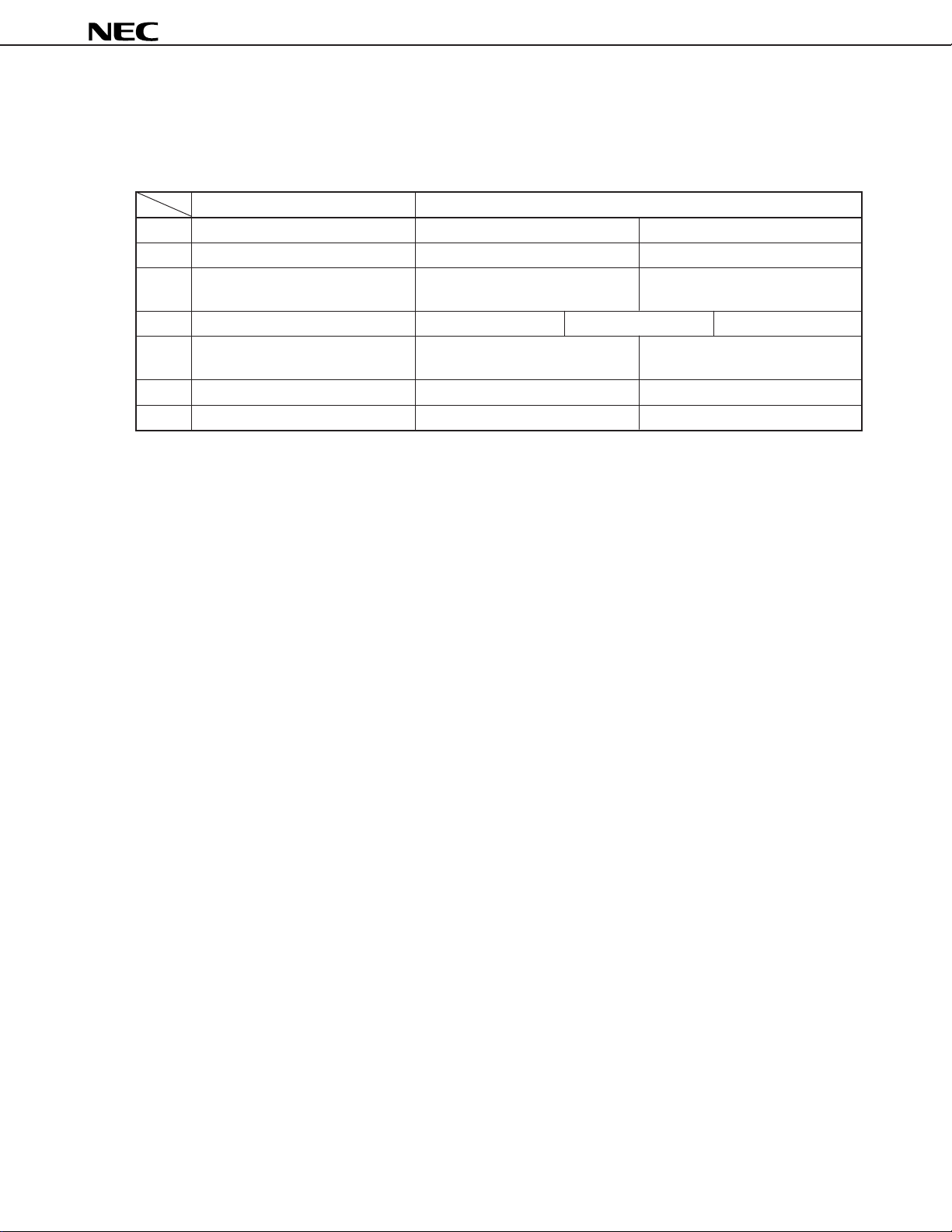
The µPD6467 selects the following parameters by using an initial status setting command.
Parameter Selected by:
(1) Dot clock LC oscillation External clock input
(2) Vertical display start position 3-row unit setting 9-row unit setting
(3) Pin selection RGB + VC1 + VC2 RGB + RGB compatible BLK
(RGB + 3BLK)
(4) Output selection Option A Option B Option C
(5) Character color reversal Black character White character
specification selection
(6) Function selection Character blinking Character left/right reversal
(7) External clock frequency selection ×1 frequency mode ×2 frequency mode
(1) Dot clock
To select a dot clock for character display. If an external clock input is selected, refer to External Clock Input
in 6. ELECTRICAL CHARACTERISTICS.
µ
PD6467
(2) Vertical display start position
To select the setting accuracy of the vertical display start position of the character display area. In 3-row units,
the vertical display start position can be set more finely than in 9-row units.
(3) Pin selection
To select the setting of the output pins.
When RGB + V
C1 + VC2 is selected, character signals are output from pins VR, VG, VB, VBLK, VC1, BLK1, VC2,
and BLK2. When RGB + 3BLK is selected, character signals are output from pins VR, VG, VB, RBLK, GBLK, BBLK,
VC1, and BLK1.
When RGB + V
C1 + VC2 is selected with a video camera with a color view finder, colored characters can be
displayed in the view finder. When RGB + 3BLK is selected, character signals can be separated color
specification.
(4) Output selection
To set the output format of the character signal where the setting of the output pin is RGB + V
C1 + VC2 (setting
the output format of the character signal is invalid where the setting of the output pin is RGB + 3BLK).
When an on-screen character display IC is used in a video camera, some items of information (such as date
and title) are displayed on the video tape, and the others (such as battery alarm, focus, and counter indication)
µ
are only displayed in the view finder. The
PD6467 can select these items of information in row or half-row
units by using the output pin. Select the output format from three types: option A, option B, and option C (when
3BLK is selected, however, be sure to select option B).
Data Sheet S14455EJ1V0DS00
9

(5) Character color reversal specification selection
To select the specifications when the character color is reversed (valid only for RGB output).
• Black character: Outputs an area with dots in black and prohibits framing.
• White character: Outputs an area with dots in white and prohibits framing.
(6) Function selection
To select either of the character blinking or character left/right reversal functions.
(7) External clock frequency selelction
µ
The external clock frequency 2 divided function is built in the
• ×1 frequency mode: External clock frequency is not divided by 2 in the
• ×2 frequency mode: External clock frequency is divided by 2 in the µPD6467.
When the dot clock control bit (OSC) is “1 (External clock input)”, this function is able to use.
Example If ×2 frequency mode is selected, and the external input frequency is 14 MHz, the internal dot clock
frequency is become to 7 MHz.
PD6467.
µ
PD6467.
µ
PD6467
The default setting assumed on power application is as follows:
(1) Dot clock = LC oscillation
(2) Vertical display start position = 3-row unit
(3) Pin selection = RGB + V
(4) Output selection = Option B
(5) Character color reversal specification selection = Black characters
(6) Function selection = Character blinking
(7) External clock frequency selection = ×1 frequency mode
C1 + VC2
10
Data Sheet S14455EJ1V0DS00
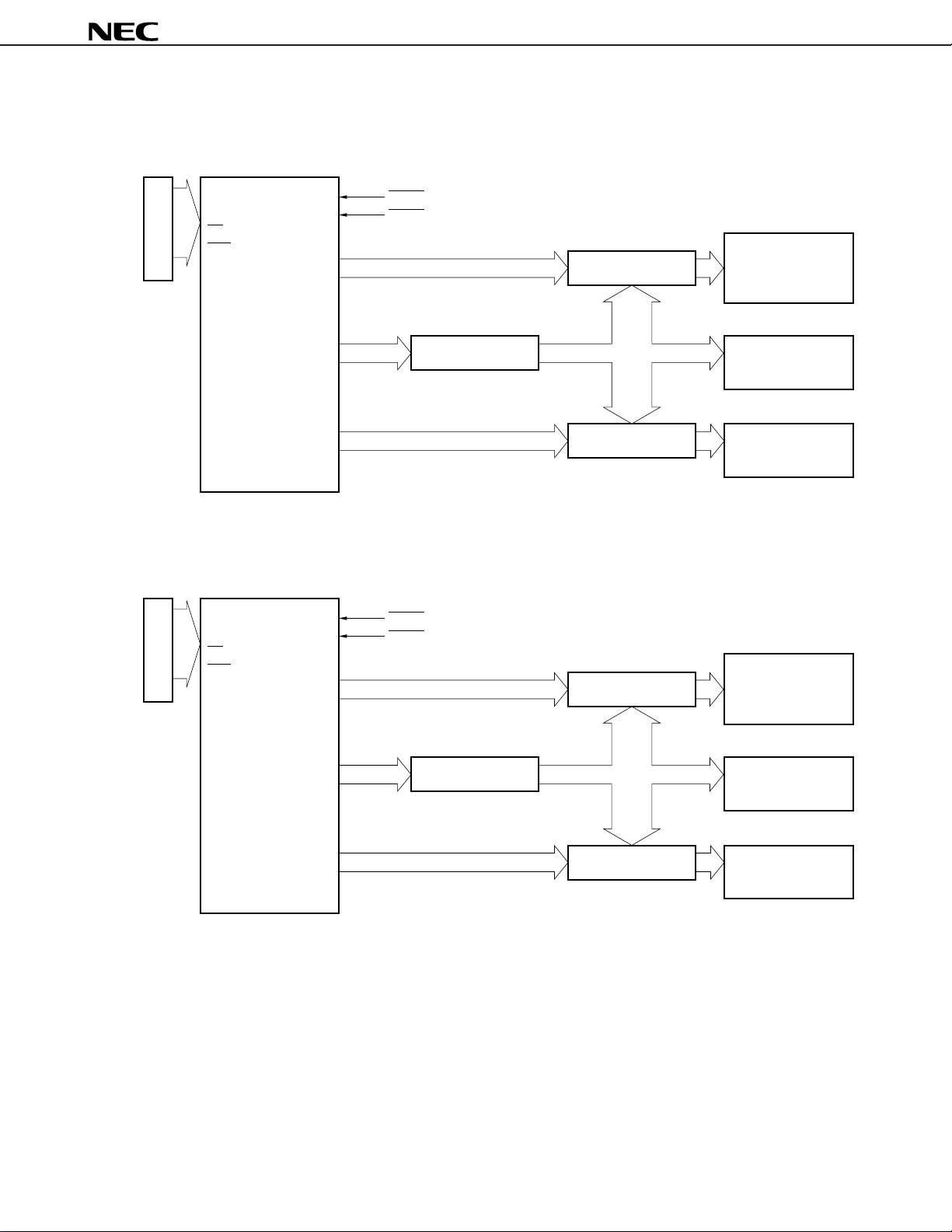
1.2 Application Block Diagram
Example of application in a video camera (1) (in the case of RGB + VC1 + VC2)
(When V
R, VG, VB, VBLK, VC1, BLK1, VC2, and BLK2 pins are used)
µ
PD6467
DATA
CLK
CS
PCL
Microcontroller
PD6467
µ
RGB
C2
V
V
C1
Hsync
Vsync
Video
Character
mixing circuit
RGB : VR, VG, VB, V
Character
mixing circuit
Video+character
Character
mixing circuit
BLK
VC1 : VC1, BLK1 VC2 : VC2, BLK2
Example of application in a video camera (2) (RGB + 3BLK (RGB compatible BLK))
(When VR, VG, VB, RBLK, GBLK, and BBLK pins are used)
DATA
CLK
CS
PCL
Microcontroller
Hsync
Vsync
R
Character
mixing circuit
Color view finder
Recording block
(deck block)
Monitor pin block
(video signal output)
Color view finder
PD6467
µ
Video
Video
G
B
Character
mixing circuit
R : VR, R
Video+character
Character
mixing circuit
BLK
G : VG, G
Video
BLK
B : VB, B
Recording block
(deck block)
Monitor pin block
(video signal output)
BLK
Data Sheet S14455EJ1V0DS00
11
µ
PD6467
1.3 Display with RGB + VC1 + VC2 Pins
The µPD6467 has three output options: A, B, and C. The following figure shows the output with each option
specified (the output is controlled by an output pin control command (refer to 3.11 Output Pin Control Command)).
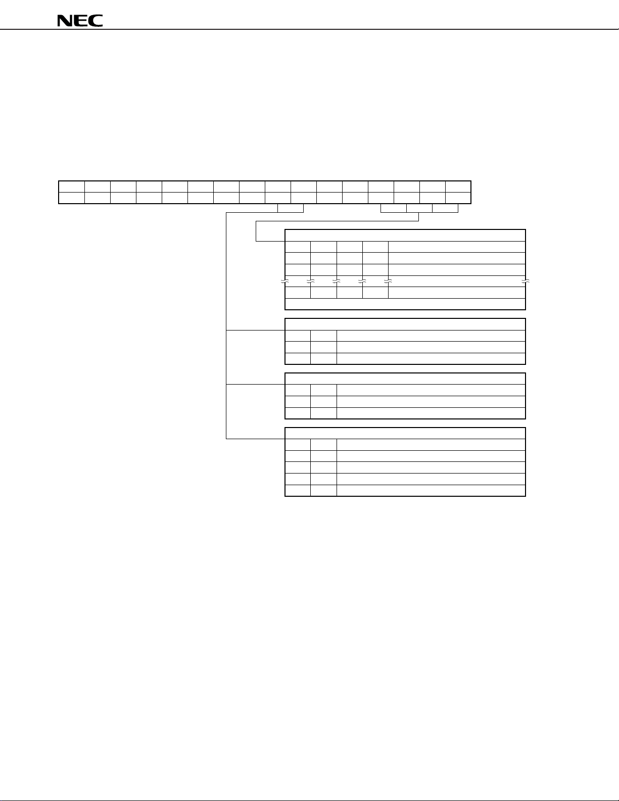
Output pin control command (with MSB first (The command is input from the MSB (D15).)
(because this command is a 2-byte command, input of 16 bits is necessary when this command is input more than
once successively.)
(MSB) (LSB)
D15 D14 D13 D12 D11 D10 D9 D8 D7 D6 D5 D4 D3 D2 D1 D0
10011100OD1OD000AR3AR2AR1AR0
Row specification bits
AR0
AR1
AR2
AR3
0
0
1
0
0
0
1
0
0
1
1
0
Setting prohibited
Function
Specifies row 0.
Specifies row 1.
Specifies row 11.
Option A
Option B
Option C
OD1
0
0
OD1
0
0
OD1
0
0
1
1
OD0
0
1
OD0
0
1
OD0
0
1
0
1
Output pin control bits
Pin output
C1
: Outputs specified row, VC2: Fixed to low level
V
V
C1
: Fixed to low level, VC2: Outputs specified row
Output pin control bits
Pin output
V
C1
: Outputs all rows, VC2: Fixed to low level
V
C1
: Outputs all rows, VC2: Outputs specified row
Output pin control bits
Pin output
C1
: Outputs columns 0-27, VC2: Fixed to low level
V
VC1: Outputs columns 0-11, VC2: Outputs columns 12-27
V
C1
: Outputs columns 12-27, VC2: Outputs columns 0-11
VC1: Fixed to low level, VC2: Outputs columns 0-27
• Row specification control
Specify whether the character signal is output to the VC1 or VC2 pin in row units (or 12-column, 16-column units).
• Output pin control
The output of the V
C1 and VC2 pins can be selected from three types, A, B, and C, by using the initial status setting
command (the blanking signal is output in the same manner).
12
Data Sheet S14455EJ1V0DS00
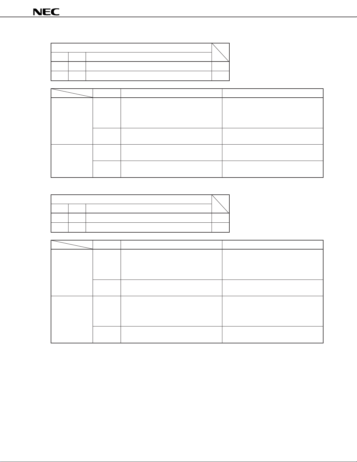
Output with option A
Output pin control bit
OD1 OD0 Pin output
00VC1: Outputs specified row, VC2: Fixed to low level (1)
01VC1: Fixed to low level, VC2: Outputs specified row (2)
µ
PD6467
Output Character signal
In the case of (1) VC1 output Outputs character signal resulting from Outputs background signal to area other
ORing VR, VG, and VB pins (specified row). than that specified by VC2.
However, character specified by VC2 is not
output.
VC2 output Fixed to low level (specified row) Outputs background signal to only area
In the case of (2) VC1 output Fixed to low level (specified row) Outputs background signal to area other
VC2 output Outputs character specified by VC2 Outputs background signal to only area
(specified row) specified by VC2
Background signal (with background specified)
specified by VC2
than that specified by VC2
Output with option B
Output pin control bit
OD1 OD0 Pin output
00VC1: Outputs all rows, VC2: Fixed to low level (1)
01VC1: Outputs all rows, VC2: Outputs specified row (2)
Output Character signal
In the case of (1) VC1 output Outputs character signal resulting from Outputs background signal to area other
ORing VR, VG, and VB pins (all rows). than that specified by VC2.
However, character specified by VC2 is not
output.
VC2 output Fixed to low level (specified row) Outputs background signal to only area
In the case of (2) VC1 output Outputs character signal resulting from Outputs background signal to area other
ORing VR, VG, and VB pins (all rows). than that specified by VC2.
However, character specified by VC2 is not
output.
VC2 output Outputs character specified by VC2 Outputs background signal to only area
(specified row). specified by VC2.
Background signal (with background specified)
specified by VC2.
Data Sheet S14455EJ1V0DS00
13
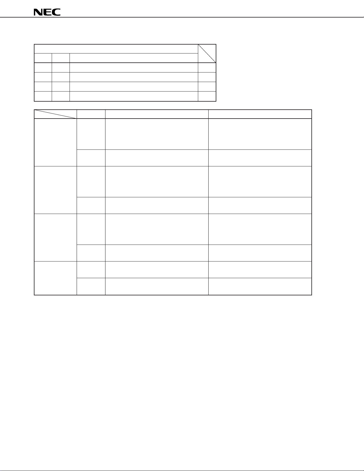
Output with option C
Output pin control bit
OD1 OD0 Pin output
00VC1: Outputs columns 0-27, VC2: Fixed to low level (1)
01VC1: Outputs columns 0-11, VC2: Outputs columns 12-27 (2)
10VC1: Outputs columns 12-27, VC2: Outputs columns 0-11 (3)
11VC1: Fixed to low level, VC2: Outputs columns 0-27 (4)
µ
PD6467
Output Character signal
In the case of (1) VC1 output Outputs character signal resulting from Outputs background signal to area other
ORing VR, VG, and VB pins (columns 0-27 of than that specified by VC2.
specified row). However, character specified
by VC2 is not output.
VC2 output Fixed to low level (specified row) Outputs background signal to only area
In the case of (2) VC1 output Outputs character signals resulting from Outputs background signal to area other
ORing VR, VG, and VB pins (columns 0-11 of than that specified by VC2.
specified row). However, character specified
by VC2 is not output.
VC2 output Outputs character specified by VC2 (columns Outputs background signal to only area
12-27 of specified row). specified by VC2.
In the case of (3) VC1 output Outputs character signal resulting from Outputs background signal to area other
ORing VR, VG, and VB pins (columns 12-27 of than that specified by VC2.
specified row). However, character specified
by VC2 is not output.
VC2 output Outputs character specified by VC2 (columns Outputs background signal to only area
0-11 of specified row). specified by VC2.
In the case of (4) VC1 output Fixed to low level (specified row) Outputs background signal to area other
VC2 output Outputs character specified by VC2 (columns Outputs background signal to only area
0-27 of specified row). specified by VC2.
Background signal (with background specified)
specified by VC2.
than that specified by VC2.
The signal of the character specified by VC2 is not output from the RGB or VC1 output channel, but the background
is output as described above.
µ
When the
PD6467 is set to output RGB, VC1, or VC2 signal, the following setting can be performed as well as the
above output control.
• Independent ON/OFF control of character display of each channel (3-channel independent display ON/OFF
command)
• Independent background control of each channel (3-channel background control command)
14
Data Sheet S14455EJ1V0DS00
µ
REC TAPE
BATT
1/1000
0000
RGB character output
(color character)
Character output of VC2 channel
(specified row, character specified by V
C2
)
AM 11:30
2000. 2.22
YOKOHAMA
BAY BRIDGE
REC TAPE
BATT
1/1000
0000
Character output of V
C1
channel
(specified row)
• Character information on the row
specified by clearing the OD0 bit to 0 is
output from V
C1
. However, the
characterspecified by V
C2
is not output.
• The row specified by setting the OD0
bit to 1 is not output (fixed to low level).
• The row specified by clearing the OD0
bit to 0 is not output (fixed to low level).
• Only the character information specified
by V
C2
on the row specified by setting
the OD0 bit to 1 is output from V
C2
.
• The character specified to V
C2
is not
output.
PD6467
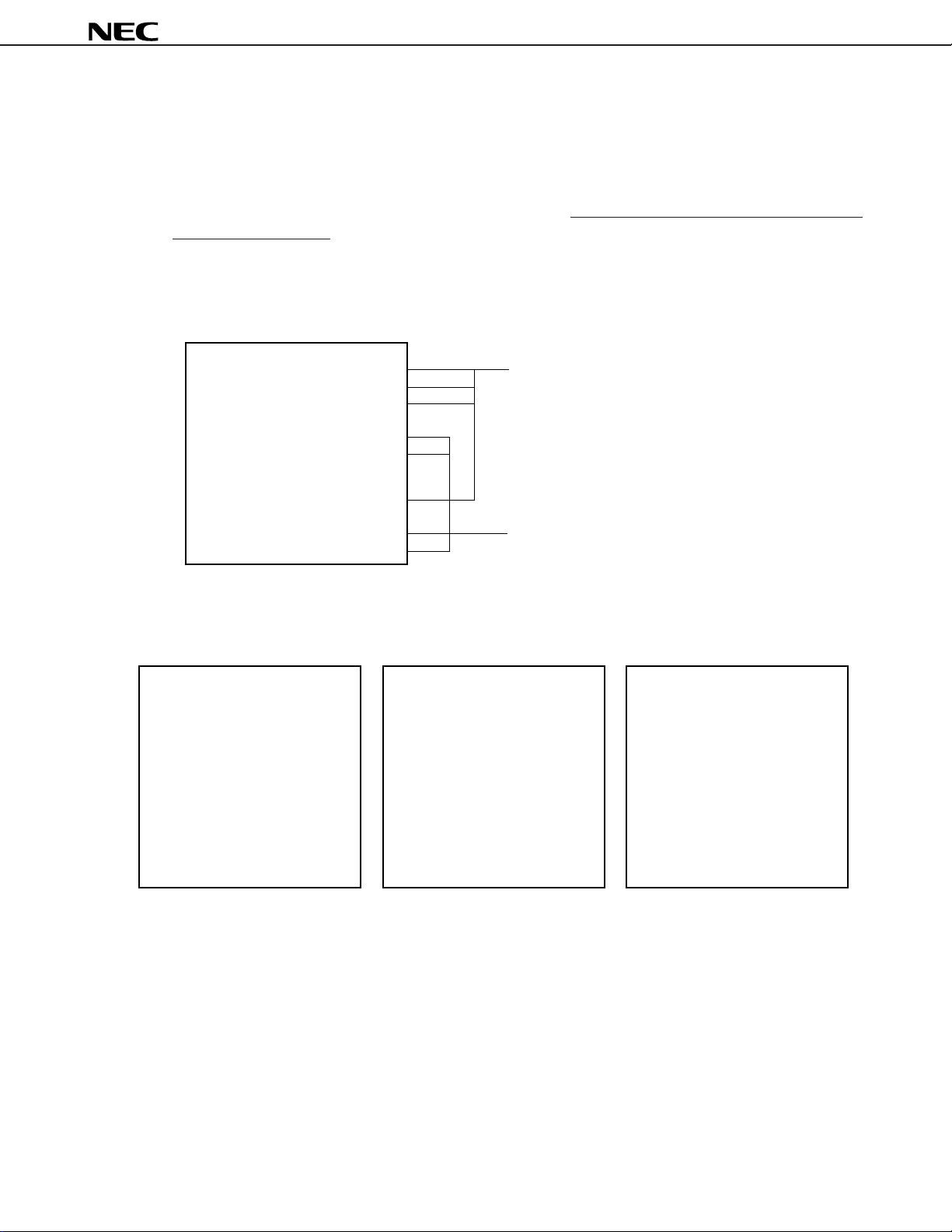
1.3.1 Character signal output with output select option A
Option A
Whether a signal is output to the character signal output pin V
C1 in row units can be specified by the OD0 bit
that selects an output pin. The VC2 output can be specified in character units, and the VC1 outputs only characters
for which the V
C2 in the rows for which the OD0 bit is set to 1. The character specified by VC2 is not output to
the RGB and VC1 output.
Display example (to use V
Example of view finder display
(RGB and V
C2
output)
REC TAPE
YOKOHAMA
BAY BRIDGE
Output example
C2 channel for information for recording)
Displayed information such as alarm and tape counter
BATT
1/1000
0000
AM 11:30
Recording information such as date and title
2000. 2.22
Data Sheet S14455EJ1V0DS00
15
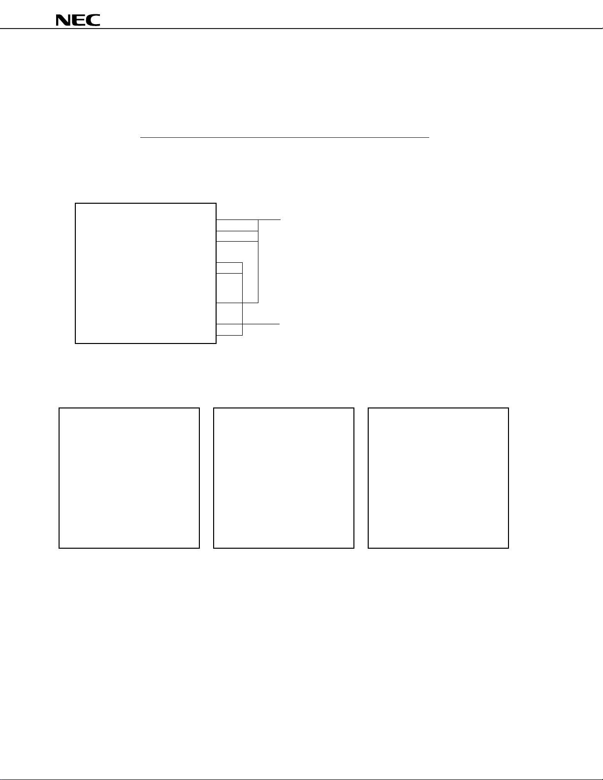
1.3.2 Character signal output with output select option B
Option B
C1 outputs characters of all rows regardless of setting of the OD0 and OD1 bits. The VC2 output can be
The V
specified in character units, and the VC2 outputs only characters for which the VC2 in the rows for which the OD0
bit is set to 1. The character specified to V
C2 is not output to the RGB and VC1 output.
Display example (to use VC2 channel for information for recording)
Example of view finder display
(RGB and V
C2
output)
µ
PD6467
REC TAPE
RAIN
YOKOHAMA
BAY BRIDGE
AM 11:30
2000. 2.22
Output example
RGB character output
(color character)
REC TAPE
BATT
1/1000
BATT
1/1000
0000
Displayed information such as alarm and tape counter
Recording information at the leftmost position (e.g., weather).
Recording information such as date and title
Character output of V
C1
channel
(all rows)
REC TAPE
BATT
1/1000
Character output of VC2 channel
(specified row, character specified to V
RAIN
YOKOHAMA
BAY BRIDGE
C2
)
• The character specified to V
output.
16
C2
is not
0000
0000
• The character information on all the
rows is output from V
C1
regardless of
the OD0 bit. However, the character
specified to V
C2
is not output.
Data Sheet S14455EJ1V0DS00
AM 11:30
2000. 2.22
• Only the character information specified
to V
C2
on the row specified by setting
the OD0 bit to 1 is output from V
C2
.
• The character information specified to
VC2 is not output on the row specified
by clearing the OD0 bit to 0 is not
output.
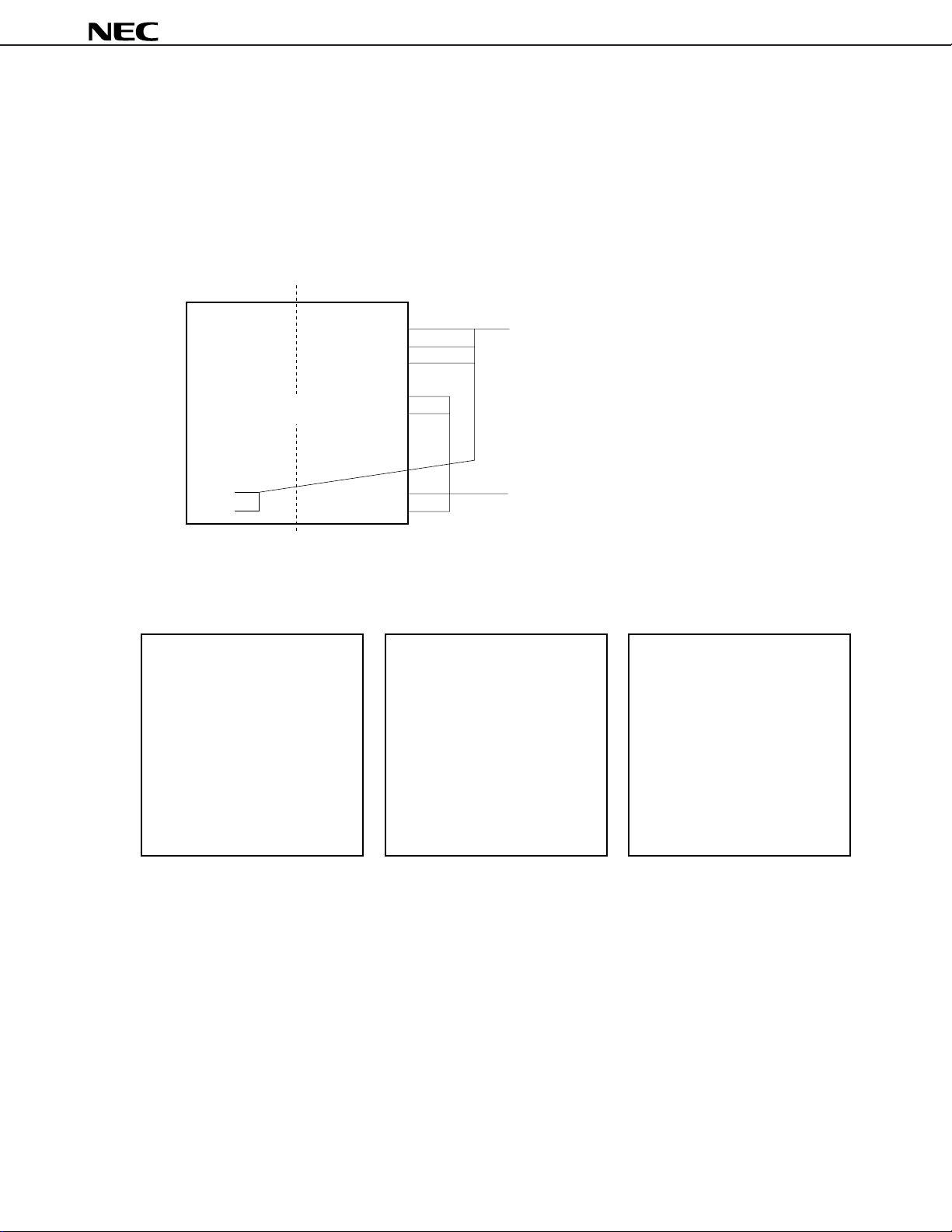
1.3.3 Character signal output with output select option C
Option C
Columns 0 through 11, and 12 through 27 on each row can be output to the V
and OD1 bits of the “output pin control command”.
Display example
Example of view finder display
0
11 12 27
µ
PD6467
C1 and VC2 pins by using the OD0
0000
REC
Output example
RGB character output
(color character)
YOKOHAMA
BAY BRIDGE
TAPE
BATT
1/1000
TAPE
BATT
1/1000
AM 11:30
2000. 2.22
Character output of V
(specified row)
Displayed information such as alarm and tape counter
Recording information such as date and title
C1
channel
Character output of VC2 channel
(character specified by V
TAPE
BATT
1/1000
YOKOHAMA
BAY BRIDGE
C2
)
0000
REC
• The character specified to V
output.
C2
is not
0000
REC
• In the case of setting OD1 bit to 0, the
C1
outputs the characters of columns
V
0 to 27 in specified rows for which the
OD0 bit is set to 0, or the characters of
columns 0 to 11 in specified rows for
which the OD0 bit is set to 1, excluding
the characters for which the V
C2
specified.
• In the case of setting OD1 bit to 1, the
V
C1
outputs the characters of columns
12 to 27 in specified rows for which
the OD0 bit is set to 0, and the rows for
which the OD0 bit is set to 1 are not
output (the V
C1
pin is fixed to low level),
excluding the characters for which the
V
C2
specified.
Data Sheet S14455EJ1V0DS00
AM 11:30
2000. 2.22
• In the case of setting OD0 bit to 0, the
C2
outputs the characters of columns
V
0 to 11 in specified rows for which the
OD1 bit is set to 1, and the rows for
which the OD1 bit is set to 0 are not
output (the V
C2
pin is fixed to low level).
• In the case of setting OD0 bit to 1, the
V
C2
outputs the characters of columns
12 to 27 in specified rows for which the
OD1 bit is set to 0, or the characters of
columns 0 to 27 in specified rows for
which the OD1 bit is set to 1.
17
µ
PD6467
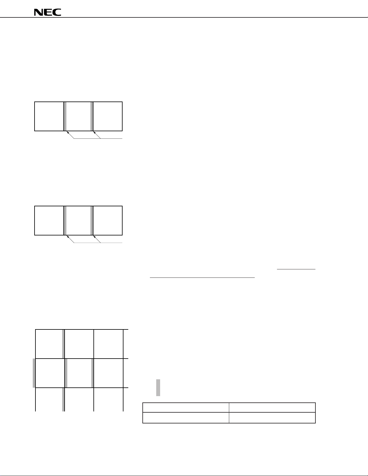
1.3.4 Displaying characters specified by VC2
The characters specified by VC2 by the display character control command are not output to the RGB and VC1 output
channels (the RGB and V
C1 output channels display
Note
the same manner as when Display Off Data is written).
Therefore, even if a background is specified by the RGB and VC1 output channel (no background/filled background),
no background is displayed at the specified portion.
Note The display is slightly different from Display Off Data.
Filling
Data
Filling
Data
Display
Off
Data
VC2-specified
character
area
Filling
Data
Filling
Data
Filling data: Character filling all 12 × 18 dots
• When Display Off Data is displayed with RGB, V
C1, and VC2
channel
In the case of Display Off Data, framing (or background, if any) of
adjacent characters is displayed with the framing or background
overlapping the area of Display Off Data by one dot of the minimum
size (the framing overlaps the area of Display Off Data, when there
are dots at the leftmost or rightmost position of the adjacent character
area).
• Displaying character area specified by V
C2 with RGB and VC1
channels
In the case of a character specified by V
C2, the framing of the adjacent
characters is displayed with the framing overlapping the VC2-specified
character area by one dot of the minimum size, but the background
does not overlap to the V
C2-specified area.
• Displaying VC2-specified character area with VC2 channel
Even if the V
C2-specified character exists with the VC2 output, the
framing also overlaps the adjacent character area, but the background
does not (the framing overlaps the VC2-specified character area, when
there are dots at the leftmost or rightmost position of the adjacent
character area).
(2)
18
VC2-specified
character
area
Filling
Data
Display
Off
Data
(1)
(3) (4)
(5)
Filling
Data
Display
Off
Data
Filling
Data
Filling
Data
C2 character specification area exists at the edge of display
• If V
area
(The figure shows the leftmost position of the display area. The same
applies to the rightmost position of the display area.)
Portion output with framing or background overlapping
(Width is 1 dot of the minimum character width.)
Portion where framing overlaps Portion where background overlaps
(1)-(5) (2)-(5)
The background is not output overlapping the VC2-specified character
area.
Data Sheet S14455EJ1V0DS00
µ
PD6467
2. COMMAND
2.1 Command Format
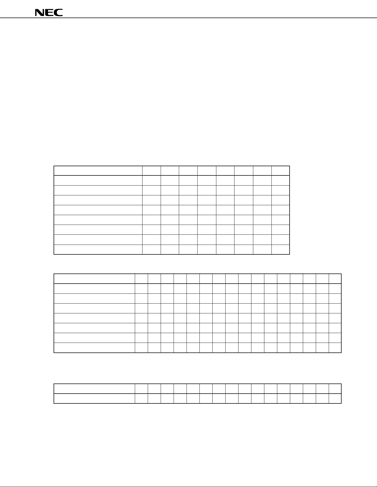
Control commands can be serially input in 8-bit units. The word length of a command is variable.
Three types of commands are available: 1-byte commands that consist of 8 bits including the instruction and data,
2-byte commands, and 2-byte successive commands that can be input in an abbreviated form.
Inputting command data with the MSB first or LSB first can be selected by using the CMDCT pin.
When the CMDCT pin is high, the data is input with the MSB first; when it is low, the data is input with the LSB
first.
2.2 Command List
(1) MSB first
1-byte commands (MSB)
Function D7 D6 D5 D4 D3 D2 D1 D0
Video RAM batch clear 00000000
Display control 0001DOLCBL1BL0
Background color/frame color control 0010RGBBFC
3-channel independent display ON/OFF
Character color reverse ON/OFF 0111100BCRE
Blue back ON/OFF 01111CLR0BB
Character address bank select 0111111BC
Output switch control 0 1 0 S3A S3B SW4 SW2 SW1
01110DOADOBDOC
2-byte commands (MSB)
Function D15 D14 D13 D12 D11 D10 D9 D8 D7 D6 D5 D4 D3 D2 D1 D0
Character display position control 100000V4V3V2V1V0H4H3H2H1H0
Write address control 1000100AR3AR2AR1AR0AC4AC3AC2AC1AC0
Output pin control 10011100OD1OD000AR3AR2AR1AR0
Character size control 100110SV1SV0SH1SH000AR3AR2AR1AR0
3-channel background control 1011001BA1BA0BFABB1BB0BFBBC1BC0BFC
Initial status setting 101101ECK00BRRSOP1OP0COCVSTOSC
Test mode
Note
10110000T7T6T5T4T3T2T1T0
Note Must not be used.
2-byte successive command (MSB)
Function D15 D14 D13 D12 D11 D10 D9 D8 D7 D6 D5 D4 D3 D2 D1 D0
Display character control 1 1 RV R G B BL VC2 C7 C6 C5 C4 C3 C2 C1 C0
Data Sheet S14455EJ1V0DS00
19
µ
PD6467
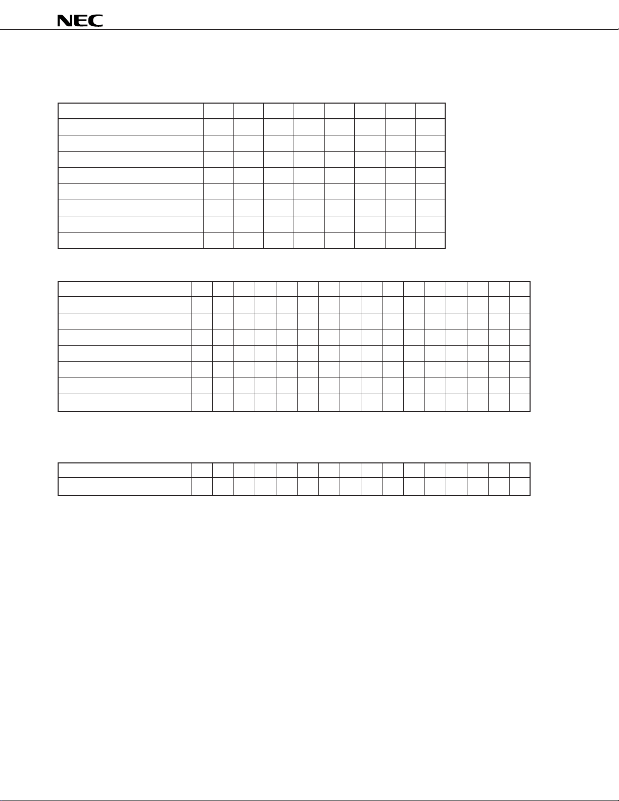
(2) LSB first
1-byte commands (LSB)
Function D0 D1 D2 D3 D4 D5 D6 D7
Video RAM batch clear 00000000
Display control BL0 BL1 LC DO 1000
Background color/frame color control BFC B G R 0100
3-channel independent display ON/OFF
Character color reverse ON/OFF BCRE 0011100
Blue back ON/OFF BB 0 CLR 11110
Character address bank select BC 1111110
Output switch control SW1 SW2 SW4 S3B S3A 0 1 0
DOCDOBDOA01110
2-byte commands (LSB)
Function D0 D1 D2 D3 D4 D5 D6 D7 D8 D9 D10 D11 D12 D13 D14 D15
Character display position control V3 V4 000001H0H1H2H3H4V0V1V2
Write address control AR3 0010001AC0AC1AC2AC3AC4AR0AR1AR2
Output pin control 00111001AR0AR1AR2AR300OD0OD1
Character size control SV0 SV1 011001AR0AR1AR2AR300SH0SH1
3-channel background control BA1 1001101BFCBC0BC1BFBBB0BB1BFABA0
Initial status setting 0 ECK 101101OSCVSTCOCOP0OP1RSBR0
Test mode
Note
00001101T0T1T2T3T4T5T6T7
Note Must not be used.
2-byte successive command (LSB)
Function D0 D1 D2 D3 D4 D5 D6 D7 D8 D9 D10 D11 D12 D13 D14 D15
Display character control VC2 BL B G R RV 1 1 C0C1C2C3C4C5C6C7
20
Data Sheet S14455EJ1V0DS00

µ
PD6467
2.3 Power-ON Clear Function
Because the internal status of the IC is undefined on power application, execute power-ON clear by lowering the
PCL pin for the duration described below.
Command setting on power-ON clear is as follows:
• Clears test mode
• Default setting of initial status (Refer to 3.14 Initial Status Setting Command.)
• Clears all character data (12 rows, 28 columns) of video RAM (Display Off Data (FEH)). No data blinks.
• Video RAM write address (row 0, digit 0)
• Standard size for all rows as character size (SV1, SV0, SH1, SH0) = (0, 0, 0, 0)
• All rows specified for output pin selection (OD1, OD0) = (0, 0)
• Display OFF, LC oscillation ON, blinking OFF
• Display of each channel OFF
• No background and framing for all three channels
• Character color reversing OFF
• Character left and right reverse OFF
• Blue back OFF
• Low-order (0) bank for character address
• Output switch control is only SW1 = ON, others OFF (S3A, S3B, SW4, SW2, SW1) = (1, 0, 0, 0, 1)
The time required for power-ON clear can be calculated by the following expression. Do not input any command
during this time.
Note
PCLL
t (Time required for power-ON clearing) = t
+ Video RAM clear time
= 10 (µs) + 10 (µs) + 12/fOSC (MHz) × 336
= 10 (µs) + 10 (µs) + 24/fOSC2 (MHz) × 336
OSC (MHz): LC oscillation frequency or external input clock frequency (when ×1 frequency mode
f
is selected)
OSC2 (MHz): External input clock frequency (when ×2 frequency mode is selected)
f
Note Refer to Power-ON Clear Specifications in 6. ELECTRICAL CHARACTERISTICS.
To clear the video RAM, the dot clock (OSC
IN pin) must be input. Be sure to input the clock when the input of an
external clock is selected.
Data Sheet S14455EJ1V0DS00
21
 Loading...