DATA SHEET
MOS INTEGRATED CIRCUIT
µ
PD6379, 6379A, 6379L, 6379AL
2-CHANNEL 16-BIT D/A CONVERTER FOR AUDIO APPLICATION
The µPD6379 and 6379A are 2-channel 16-bit D/A converters for digital audio signal demodulation. These D/A
µ
converters employ the resistor string conversion method which has been tested by existing model
are more compact and require fewer external components than the µPD6376. In addition, low-voltage models, the
µ
PD6379L and 6379AL (minimum operating supply voltage = +3.0 V) are also available for applications in portable
systems.
FEATURES
• Resistor string conversion method
• 0-point digital shift circuit
• × 4 oversampling
Sampling frequency: 200 kHz MAX.
• Signal processing format for 2’s complement, MSB first, and backward justification data accommodated
• Left and right in-phase output
• High performance (at V
S/N ratio: 100 dB TYP.
Dynamic range: 96 dB TYP.
• Low-voltage models available
• Bipolar LR clock (LRCK)
• Low power dissipation:10 mW TYP.
µ
PD6379L, 6379AL at VDD = +3.3 V)
(with
DD = +5.0 V)
PD6376 but they
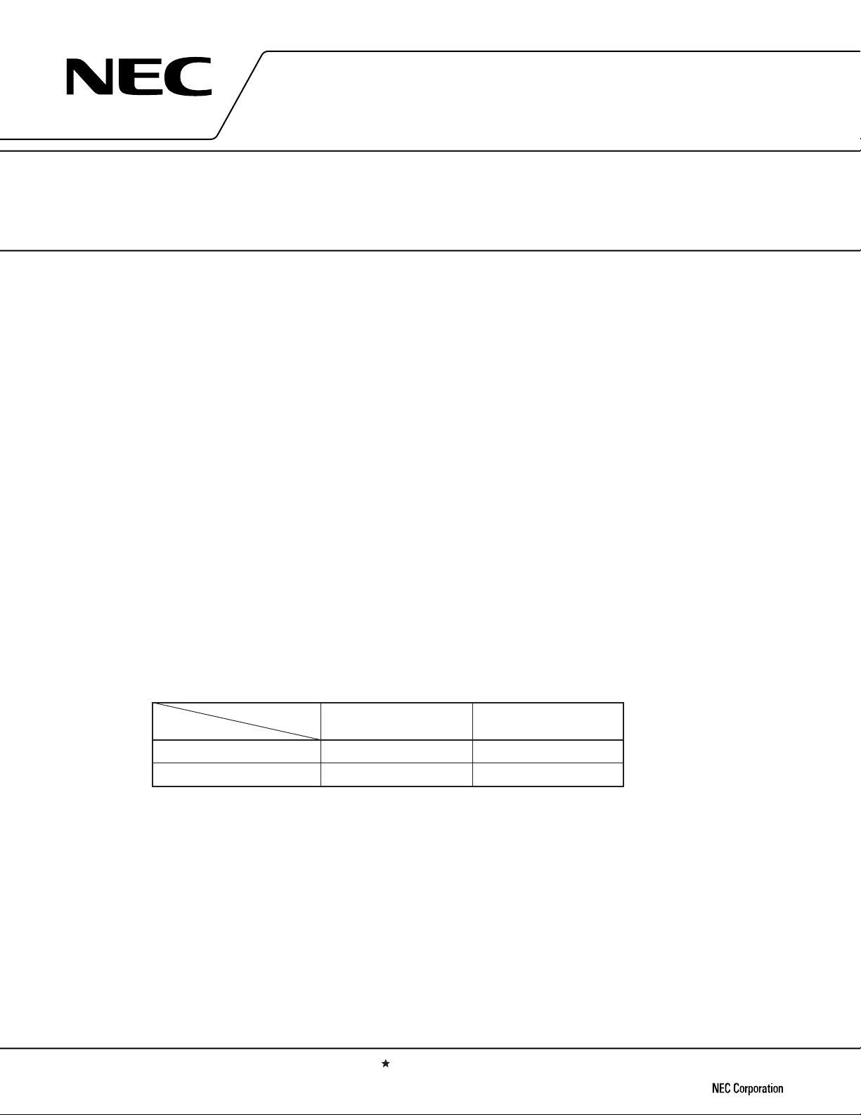
Supply voltage when L-ch data is input when L-ch data is input
+3.3 V (VDD = +3.0 to 5.5 V)
+5.0 V (VDD = +4.5 to 5.5 V)
• Few external components
Internal output operational amplifier
Only one electrolytic capacitor required for smoothing reference voltage, instead of two capacitors required by
existing D/A converters
• Small package: 8-pin plastic SOP (5.72 mm (225))
The information in this document is subject to change without notice. Before using this document, please
confirm that this is the latest version.
Not all devices/types available in every country. Please check with local NEC representative for availability
and additional information.
Document No. S11588EJ4V0DS00 (4th edition)
Date Published November 1999 N CP(K)
Printed in Japan
LRCK LRCK = L LRCK = H
µ
PD6379L
µ
PD6379
The mark shows major revised points.
µ
PD6379AL
µ
PD6379A
©
1996

ORDERING INFORMATION
Part number Package
µ
PD6379GR 8-pin plastic SOP (5.72 mm (225))
µ
PD6379LGR 8-pin plastic SOP (5.72 mm (225))
µ
PD6379AGR 8-pin plastic SOP (5.72 mm (225))
µ
PD6379ALGR 8-pin plastic SOP (5.72 mm (225))
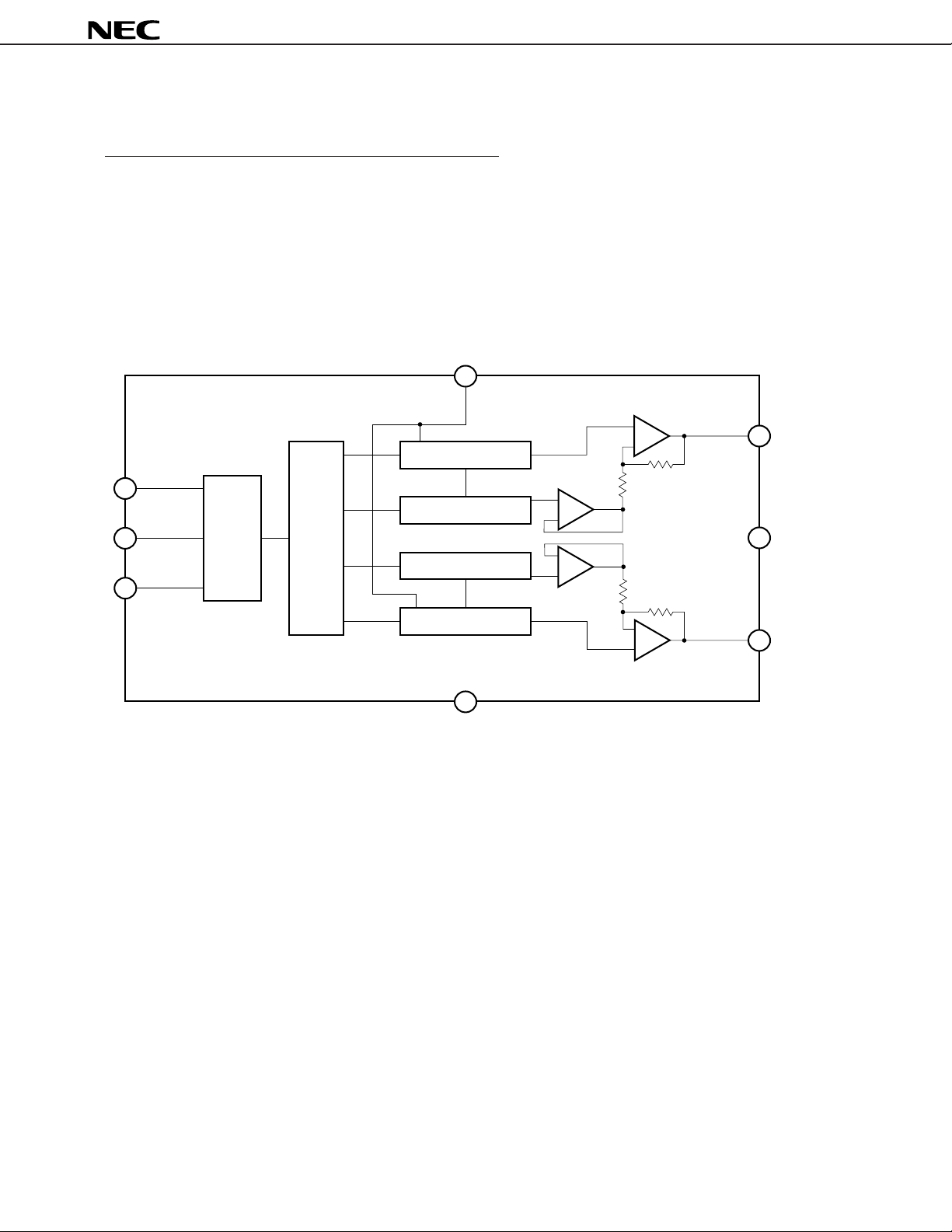
BLOCK DIAGRAM
REF
Main DAC
µ
PD6379, 6379A, 6379L, 6379AL
L. OUT
LRCK
CLK
Sub DAC
GND
Timing
generator
SI
Shift register latch
Sub DAC
Main DAC
V
DD
R. OUT
2
Data Sheet S11588EJ4V0DS00

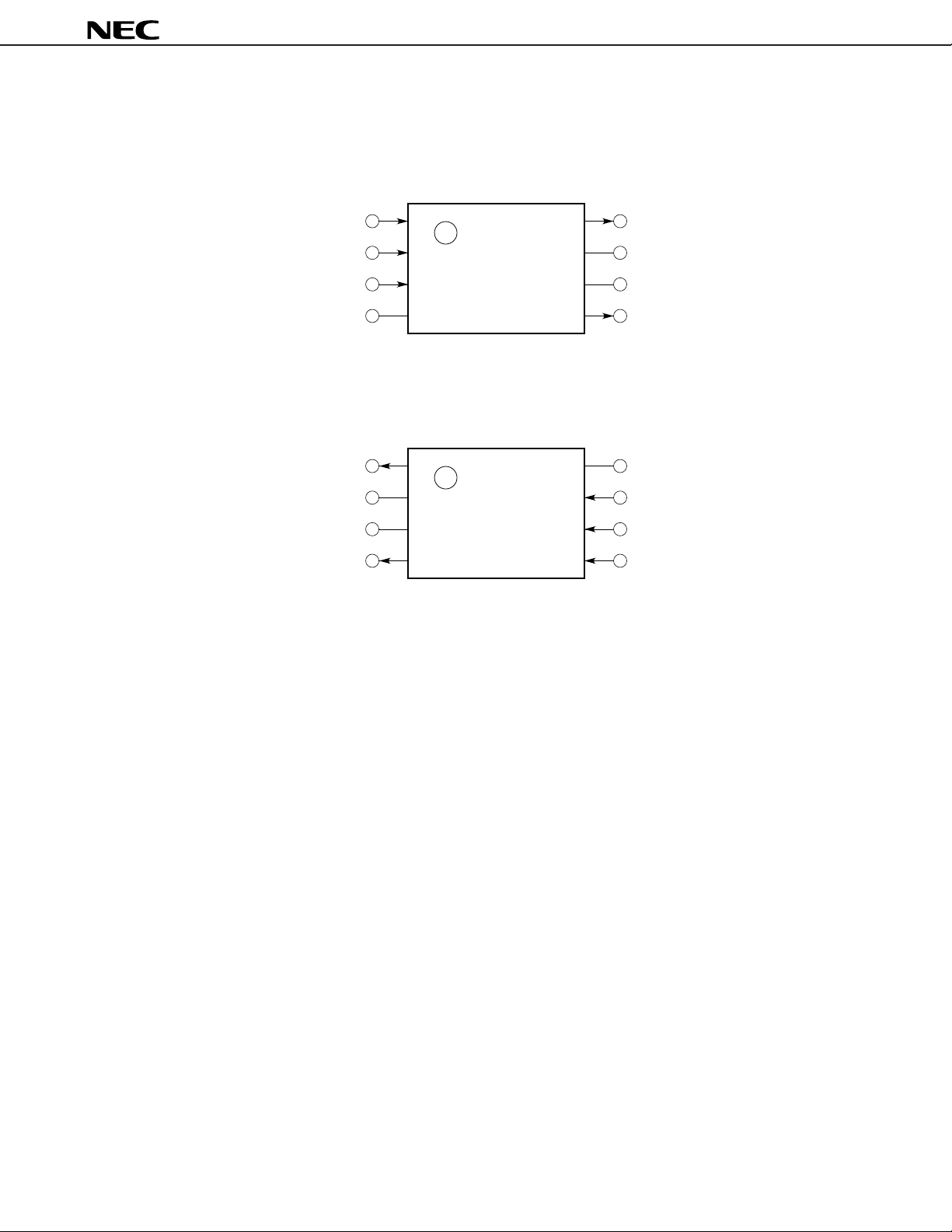
PIN CONFIGURATIONS (Top View)
8-pin plastic SOP (5.72 mm (225))
•µPD6379GR, 6379LGR
µ
PD6379, 6379A, 6379L, 6379AL
LRCK
CLK
V
1
SI
DD
2
3
4
8
7
6
5
L. OUT
GND
REF
R. OUT
•µPD6379AGR, 6379ALGR
R. OUT
REF
GND
L. OUT
1
2
3
4
8
7
6
5
DD
V
CLK
SI
LRCK
Remark The pin configuration of the µPD6379 and 6379L is different from that of the µPD6379A and 6379AL.
Data Sheet S11588EJ4V0DS00
3

µ
PD6379, 6379A, 6379L, 6379AL
1. PIN FUNCTIONS
Table 1-1 Pin Functions
Pin No.
µ
PD6379,
6379L 6379AL
1 5 Left/Right Clock LRCK Input Input pin to identify left or right input data.
2 6 Serial Input SI Input Serial data input pin.
3 7 Clock CLK Input Serial input data read clock (bit clock) input pin
4 8 Supply Voltage VDD – Positive power supply pin
5 1 R-ch Output R. OUT Output Right analog signal output pin
6 2 Reference Voltage REF – Reference voltage pin. Connect this pin to GND
7 3 Ground GND – GND pin
8 4 L-ch Output L. OUT Output Left analog signal output pin
µ
PD6379A,
Name Symbol I/O Function
µ
PD6379, 6379L: Input “L” to this pin when
inputting L-ch data to SI pin.
µ
PD6379A, 6379AL: Input “H” to this pin
inputting L-ch data to SI pin.
Input data on 2’s complement, MSB first, and
backward justification.
through capacitor.
when
4
Data Sheet S11588EJ4V0DS00

µ
PD6379, 6379A, 6379L, 6379AL
2. ELECTRICAL SPECIFICATIONS
ABSOLUTE MAXIMUM RATINGS (TA = 25 °C)
Parameter Symbol Ratings Unit
Supply voltage VDD – 0.3 to +7.0 V
Input voltage VI – 0.3 to VDD + 0.3 V
Output voltage VO – 0.3 to VDD + 0.3 V
Permissible package PD 220 (TA = 75 ˚C) mW
power dissipation
Operating ambient temperature TA –20 to +75 °C
Storage temperature Tstg –40 to +125 °C
Caution Exposure to Absolute Maximum Ratings for extended periods may affect device reliability;
exceeding the ratings could cause permanent damage. The parameters apply independently. The
device should be operated within the limits specified under DC and AC Characteristics.
Data Sheet S11588EJ4V0DS00
5
 Loading...