

Page 1
DATA SHEET
MOS INTEGRATED CIRCUIT
µµµµ
PD23C32040AL, 23C32080AL
32M-BIT MASK-PROGRAMMABLE ROM
4M-WORD BY 8-BIT (BYTE MODE) / 2M-WORD BY 16-BIT (WORD MODE)
PAGE ACCESS MODE
Description
The µPD23C32040AL and µPD23C32080AL are 33,554,432 bits mask-programmable ROM. The word organization is
selectable (BYTE mode : 4,194,304 words by 8 bits, WORD mode : 2,097,152 words by 16 bits).
The active levels of OE (Output Enable Input) can be selected with mask-option.
The
PD23C32040AL and µPD23C32080AL are packed in 48-pin PLASTIC TSOP(I) and 44-pin PLASTIC SOP.
µ
Features
• Word organization
4,194,304 words by 8 bits (BYTE mode)
2,097,152 words by 16 bits (WORD mode)
• Page access mode
PD23C32040AL)
BYTE mode : 8 byte random page access (
16 byte random page access (
WORD mode :4 word random page access (
8 word random page access (
= 2.7 V to 3.6 V
• Operating supply voltage : V
Operating supply Access time / Power supply current (Active mode) Standby current
voltage Page access time mA (MAX.) (CMOS level input)
V
CC
3.0 V ± 0.3 V 100 / 25 40 55 30
3.3 V ± 0.3 V 90 / 25
CC
ns (MAX.)
µ
PD23C32080AL)
µ
PD23C32040AL)
µ
PD23C32080AL)
µ
PD23C32040ALµPD23C32080AL
µ
A (MAX.)
µ
The information in this document is subject to change without notice. Before using this document, please
confirm that this is the latest version.
Not all products and/or types are available in every country. Please check with an NEC Electronics
sales representative for availability and additional information.
Document No. M15772EJ3V0DS00 (3rd edition)
Date Published February 2003 NS CP(K)
Printed in Japan
The mark shows major revised points.
2001
Page 2

µµµµ
PD23C32040AL, 23C32080AL
Ordering Information
Part Number Package
PD23C32040ALGY-xxx-MJH 48-pin PLASTIC TSOP(I) (12 x 18) (Normal bent)
µ
PD23C32040ALGY-xxx-MKH 48-pin PLASTIC TSOP(I) (12 x 18) (Reverse bent)
µ
PD23C32040ALGX-xxx 44-pin PLASTIC SOP (15.24 mm (600))
µ
PD23C32080ALGY-xxx-MJH 48-pin PLASTIC TSOP(I) (12 x 18) (Normal bent)
µ
PD23C32080ALGY-xxx-MKH 48-pin PLASTIC TSOP(I) (12 x 18) (Reverse bent)
µ
PD23C32080ALGX-xxx 44-pin PLASTIC SOP (15.24 mm (600))
µ
(xxx : ROM code suffix No.)
2
Data Sheet M15772EJ3V0DS
Page 3
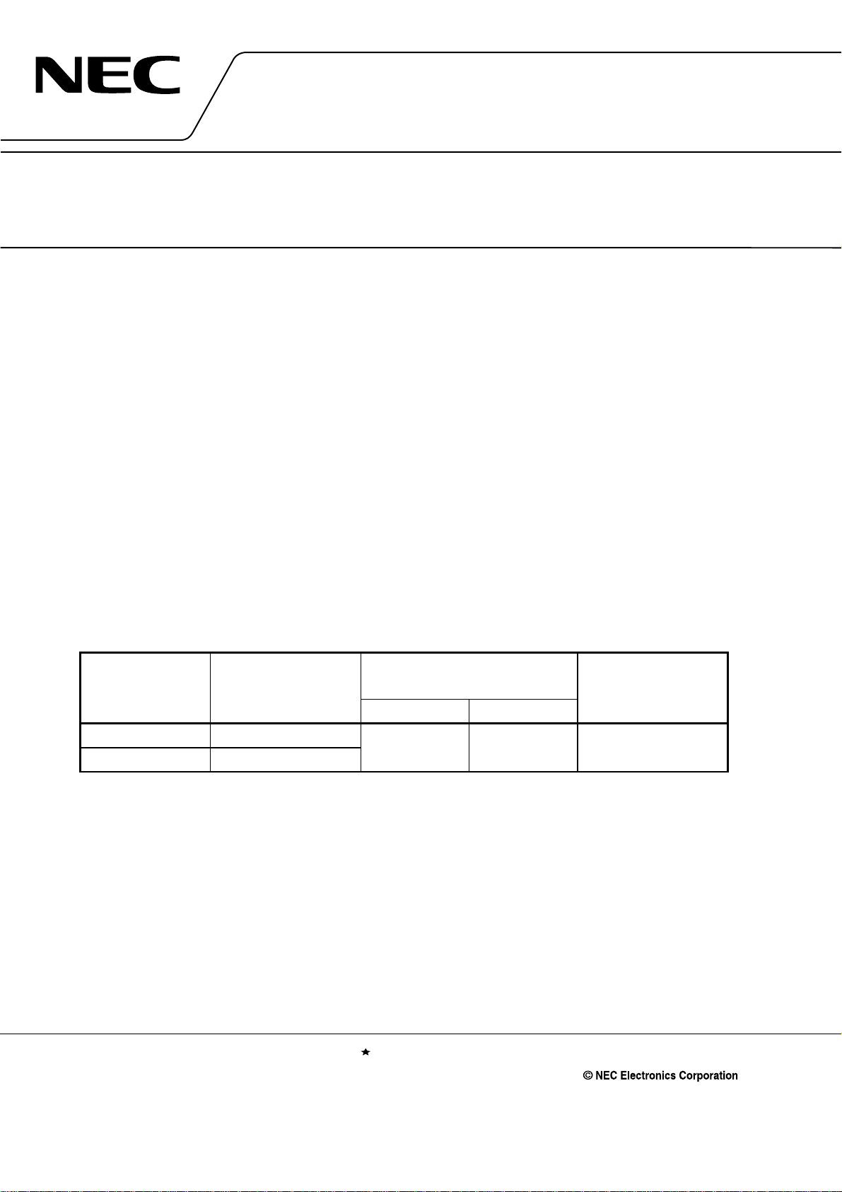
Pin Configurations
/xxx indicates active low signal.
µµµµ
PD23C32040AL, 23C32080AL
48-pin PLASTIC TSOP(I) (12 x 18) (Normal bent)
µµµµ
[
PD23C32040ALGY-xxx-MJH ]
µµµµ
PD23C32080ALGY-xxx-MJH ]
[
Marking Side
WORD, /BYTE
A16
A15
A14
A13
A12
A11
A10
A9
A8
A19
NC
A20
A18
A17
A7
A6
A5
A4
A3
A2
A1
A0
/CE
1
2
3
4
5
6
7
8
9
10
11
12
13
14
15
16
17
18
19
20
21
22
23
24
48
47
46
45
44
43
42
41
40
39
38
37
36
35
34
33
32
31
30
29
28
27
26
25
GND
GND
O15, A−1
O7
O14
O6
O13
O5
O12
O4
V
CC
V
CC
NC
O11
O3
O10
O2
O9
O1
O8
O0
/OE or OE or DC
GND
GND
A0 to A20 : Address inputs
O0 to O7, O8 to O14 : Data outputs
O15, A–1 : Data output 15 (WORD mode),
LSB Address input (BYTE mode)
WORD, /BYTE : Mode select
/CE : Chip Enable
/OE or OE : Output Enable
CC
V
: Supply voltage
GND : Ground
Note
NC
: No Connection
DC : Don’t Care
Note Some signals can be applied because this pin is not connected to the inside of the chip.
Remark Refer to Package Drawings for the 1-pin index mark.
Data Sheet M15772EJ3V0DS
3
Page 4
µµµµ
PD23C32040AL, 23C32080AL
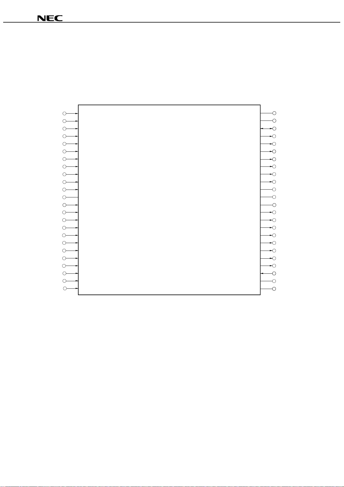
48-pin PLASTIC TSOP(I) (12 x 18) (Reverse bent)
µµµµ
PD23C32040ALGY-xxx-MKH ]
[
µµµµ
[
PD23C32080ALGY-xxx-MKH ]
Marking Side
GND
GND
O15, A−1
O7
O14
O6
O13
O5
O12
O4
V
VCC
NC
O11
O3
O10
O2
O9
O1
O8
O0
/OE or OE or DC
GND
GND
48
47
46
45
44
43
42
41
40
39
CC
38
37
36
35
34
33
32
31
30
29
28
27
26
25
1
2
3
4
5
6
7
8
9
10
11
12
13
14
15
16
17
18
19
20
21
22
23
24
WORD, /BYTE
A16
A15
A14
A13
A12
A11
A10
A9
A8
A19
NC
A20
A18
A17
A7
A6
A5
A4
A3
A2
A1
A0
/CE
A0 to A20 : Address inputs
O0 to O7, O8 to O14 : Data outputs
O15, A–1 : Data output 15 (WORD mode),
LSB Address input (BYTE mode)
WORD, /BYTE : Mode select
/CE : Chip Enable
/OE or OE : Output Enable
CC
V
: Supply voltage
GND : Ground
Note
NC
: No Connection
DC : Don’t Care
Note Some signals can be applied because this pin is not connected to the inside of the chip.
Remark Refer to Package Drawings for the 1-pin index mark.
4
Data Sheet M15772EJ3V0DS
Page 5
µµµµ
PD23C32040AL, 23C32080AL
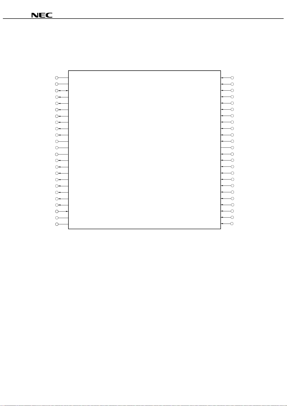
44-pin PLASTIC SOP (15.24 mm (600))
µµµµ
PD23C32040ALGX-xxx ]
[
µµµµ
[
PD23C32080ALGX-xxx ]
Marking Side
NC
A18
A17
A7
A6
A5
A4
A3
A2
A1
A0
/CE
GND
/OE or OE or DC
O0
O8
O1
O9
O2
O10
O3
O11
1
2
3
4
5
6
7
8
9
10
11
12
13
14
15
16
17
18
19
20
21
22
44
43
42
41
40
39
38
37
36
35
34
33
32
31
30
29
28
27
26
25
24
23
A20
A19
A8
A9
A10
A11
A12
A13
A14
A15
A16
WORD, /BYTE
GND
O15, A−1
O7
O14
O6
O13
O5
O12
O4
CC
V
A0 to A20 : Address inputs
O0 to O7, O8 to O14 : Data outputs
O15, A–1 : Data output 15 (WORD mode),
LSB Address input (BYTE mode)
WORD, /BYTE : Mode select
/CE : Chip Enable
/OE or OE : Output Enable
CC
V
: Supply voltage
GND : Ground
Note
NC
: No Connection
DC : Don’t Care
Note Some signals can be applied because this pin is not connected to the inside of the chip.
Remark Refer to Package Drawings for the 1-pin index mark.
Data Sheet M15772EJ3V0DS
5
Page 6
µµµµ
PD23C32040AL, 23C32080AL
Input / Output Pin Functions
Pin name Input / Output Function
WORD, /BYTE Input The pin for switching WORD mode and BYTE mode.
High level : WORD mode (2M-word by 16-bit)
Low level : BYTE mode (4M-word by 8-bit)
A0 to A20
(Address inputs)
O0 to O7, O8 to O14
(Data outputs)
O15, A−1
(Data output 15,
LSB Address input)
/CE
(Chip Enable)
/OE or OE or DC
(Output Enable, Don't care)
V
CC
GND − Ground
NC − Not internally connected. (The signal can be connected.)
Input Address input pins.
A0 to A20 are used differently in the WORD mode and the BYTE mode.
WORD mode (2M-word by 16-bit)
A0 to A20 are used as 21 bits address signals.
BYTE mode (4M-word by 8-bit)
A0 to A20 are used as the upper 21 bits of total 22 bits of address signal.
(The least significant bit (A−1) is combined to O15.)
Output Data output pins.
O0 to O7, O8 to O14 are used differently in the WORD mode and the BYTE mode.
WORD mode (2M-word by 16-bit)
The lower 15 bits of 16 bits data outputs to O0 to O14.
(The most significant bit (O15) combined to A−1.)
BYTE mode (4M-word by 8-bit)
8 bits data outputs to O0 to O7 and also O8 to O14 are high impedance.
Output, Input O15, A−1 are used differently in the WORD mode and the BYTE mode.
WORD mode (2M-word by 16-bit)
The most significant output data bus (O15).
BYTE mode (4M-word by 8-bit)
The least significant address bus (A−1).
Input Chip activating signal.
When the OE is active, output states are following.
High level : High-Z
Low level : Data out
Input Output enable signal. The active level of OE is mask option. The active level of OE
can be selected from high active, low active and Don’t care at order.
− Supply voltage
6
Data Sheet M15772EJ3V0DS
Page 7
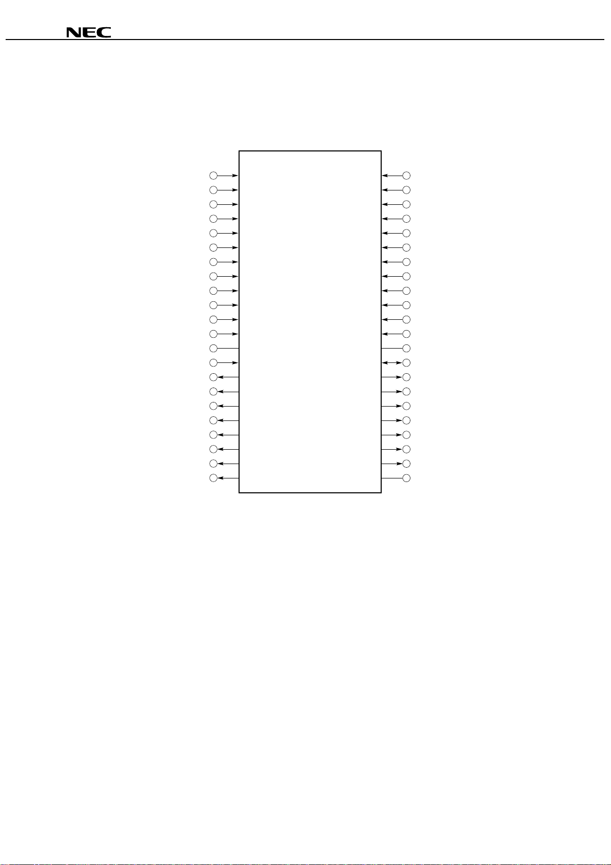
Block Diagram
µµµµ
PD23C32040AL, 23C32080AL
A0
A1
A2
A3
A4
A5
A6
A7
A8
A9
A10
A11
A12
A13
A14
A15
A16
A17
A18
A19
A20
Y-Decoder
Address Input Buffer
X-Decoder
O0
O8
O10O9
O2
O1
O3 O4
Output Buffer
Y-Selector
Memory Cell Matrix
2,097,152 words by 16 bits /
4,194,304 words by 8 bits
O12O11
O5 O6 O7
O14O13
O15, A−1
Logic/InputInput Buffer
WORD, /BYTE
/OE or OE or DC
/CE
Data Sheet M15772EJ3V0DS
7
Page 8
µµµµ
PD23C32040AL, 23C32080AL
Mask Option
The active levels of output enable pin (/OE or OE or DC) are mask programmable and optional, and can be selected
from among " 0 " " 1 " " x " shown in the table below.
Option /OE or OE or DC OE active level
0/OE L
1OE H
x DC Don’t care
Operation modes for each option are shown in the tables below.
Operation mode (Option : 0)
/CE /OE Mode Output state
L L Active Data out
H High-Z
H H or L Standby High-Z
Operation mode (Option : 1)
/CE OE Mode Output state
L L Active High-Z
H Data out
H H or L Standby High-Z
Operation mode (Option : x)
/CE DC Mode Output state
L H or L Active Data out
H H or L Standby High-Z
Remark L : Low level input
H : High level input
8
Data Sheet M15772EJ3V0DS
Page 9

Electrical Specifications
Absolute Maximum Ratings
Parameter Symbol Condition Rating Unit
µµµµ
PD23C32040AL, 23C32080AL
Supply voltage V
Input voltage V
Output voltage V
Operating ambient temperature T
Storage temperature T
CC
I
O
A
stg
–0.3 to +4.6 V
–0.3 to VCC+0.3 V
–0.3 to VCC+0.3 V
–10 to +70 °C
–65 to +150 °C
Caution Exposing the device to stress above those listed in Absolute Maximum Ratings could cause
permanent damage. The device is not meant to be operated under conditions outside the limits
described in the operational section of this specification. Exposure to Absolute Maximum Rating
conditions for extended periods may affect device reliability.
Capacitance (T
Input capacitance C
Output capacitance C
A
= 25 °C)
Parameter Symbol Test condition MIN. TYP. MAX. Unit
f = 1 MHz 10 pF
I
O
12 pF
DC Characteristics (TA = –10 to +70 °C, VCC = 2.7 to 3.6 V)
Parameter Symbol Test conditions MIN. TYP. MAX. Unit
High level input voltage V
Low level input voltage V
High level output voltage V
Low level output voltage V
Input leakage current I
Output leakage current I
Power supply current I
Standby current I
IH
V
= 3.0 V ± 0.3 V –0.3 +0.5 V
IL
OHIOH
OLIOL
LI
LO
CC1
CC3
CC
V
= 3.3 V ± 0.3 V –0.3 +0.8 V
CC
= –100 µA2.4V
= 2.1 mA 0.4 V
V
= 0 V to V
I
V
= 0 V to VCC, Chip deselected –10 +10
O
/CE = V
mode), I
CC
(ActiveµPD23C32040AL V
IL
= 0 mA V
O
PD23C32080AL V
µ
= 3.0 V ± 0.3 V 40 mA
CC
= 3.3 V ± 0.3 V 40
CC
= 3.0 V ± 0.3 V 55
CC
V
= 3.3 V ± 0.3 V 55
CC
/CE = VCC – 0.2 V (Standby mode) 30
2.0 VCC + 0.3 V
–10 +10
A
µ
A
µ
A
µ
Data Sheet M15772EJ3V0DS
9
Page 10

AC Characteristics (TA = –10 to +70 °C, VCC = 2.7 to 3.6 V)
Parameter Symbol Test condition VCC = 3.0 V ± 0.3 V VCC = 3.3 V ± 0.3 V Unit
µµµµ
PD23C32040AL, 23C32080AL
MIN. TYP. MAX. MIN. TYP. MAX.
Address access time t
Page access time t
Address skew time t
Chip enable access time t
Output enable access time t
Output hold time t
Output disable time t
WORD, /BYTE access time t
indicates the following three types of time depending on the condition.
Note t
SKEW
ACC
PAC
SKEW Note 10 10 ns
CE
OE
OH
DF
WB
1) When switching /CE from high level to low level, t
00ns
0 25 0 25 ns
is the time from the /CE low level input point until the
SKEW
100 90 ns
25 25 ns
100 90 ns
25 25 ns
100 90 ns
next address is determined.
2) When switching /CE from low level to high level, t
is the time from the address change start point to the
SKEW
/CE high level input point.
3) When /CE is fixed to low level, t
is the time from the address change start point until the next address is
SKEW
determined.
Since specs are defined for t
only when /CE is active, t
SKEW
is not subject to limitations when /CE is switched
SKEW
from high level to low level following address determination, or when the address is changed after /CE is switched
from low level to high level.
is the time from inactivation of Chip Enable input (/CE) or Output Enable input (/OE or OE) to
Remark t
DF
high impedance state output.
AC Test Conditions
Input waveform (Rise
Output waveform
Output load
1TTL + 100 pF
/
Fall time
≤
≤ 5 ns)
≤≤
Test points1.4 V 1.4 V
Test points1.4 V 1.4 V
10
Data Sheet M15772EJ3V0DS
Page 11

PD23C32040AL, 23C32080AL
µµµµ
Cautions on power application
To ensure normal operation, always apply power using /CE following the procedure shown below.
1) Input a high level to /CE during and after power application.
2) Hold the high level input to /CE for 200 ns or longer (wait time).
3) Start normal operation after the wait time has elapsed.
Power Application Timing Chart 1 (When /CE is made high at power application)
Wait time
/CE (Input)
200 ns or longer
CC
V
Power Application Timing Chart 2 (When /CE is made high after power application)
Wait time
/CE (Input)
200 ns or longer
CC
V
Caution Other signals can be either high or low during the wait time.
Normal operation
Normal operation
Data Sheet M15772EJ3V0DS
11
Page 12

Read Cycle Timing Chart 1
t
SKEW
µµµµ
PD23C32040AL, 23C32080AL
t
t
SKEW
SKEW
A0 to A20,
A−1
/OE or OE
O0 to O7,
O8 to O15
Note1
Note3
/CE
(Input)
(Input)
(Input)
(Input)
t
ACC
t
CE
t
OE
Notes 1. During WORD mode, A–1 is O15.
is the time from inactivation of Chip Enable input (/CE) or Output Enable input (/OE or OE) to
DF
2. t
high impedance state output.
3. During BYTE mode, O8 to O14 are high impedance and O15 is A–1.
t
ACC
Note2
t
DF
t
OH
Data out Data out Data out
High-ZHigh-Z
t
ACC
t
OH
t
OH
Note2
t
DF
12
Data Sheet M15772EJ3V0DS
Page 13

Read Cycle Timing Chart 2 (Page Access Mode)
µµµµ
PD23C32040AL, 23C32080AL
Upper address
A2 to A20
A3 to A20
Page address
Note 2
A–1
A–1
Note 2
, A0, A1
, A0, A1, A2
O0 to O7,
O8 to O15
Note 1
(Input)
/CE (Input)
/OE or OE (Input)
Note 1
(Input)
(Output)
Note 4
t
ACC
t
CE
tOE
Note 5
t
PAC
High-Z High-Z
Data Out
Note 5
tPAC
OH
t
tOH
Data Out Data Out
tOH
tDF
Note 3
Notes 1. The address differs depending on the product as follows.
Part Number Upper address Page address
PD23C32040AL A2 to A20 A–1, A0, A1
µ
PD23C32080AL A3 to A20 A–1, A0, A1, A2
µ
2. During WORD mode, A–1 is O15.
is the time from inactivation of Chip Enable input (/CE) or Output Enable input (/OE or OE) to
DF
3. t
high impedance state output.
4. During BYTE mode, O8 to O14 are high impedance and O15 is A–1.
5. The definition of page access time is as follows.
µµµµ
PD23C32040AL ]
[
Page access time Upper address (A2 to A20) /CE input condition /OE or OE input condition
inputs condition
t
PAC
µµµµ
[
PD23C32080AL ]
Before t
ACC
– t
PAC
Page access time Upper address (A3 to A20) /CE input condition /OE or OE input condition
inputs condition
Before tCE – t
PAC
Before stabilizing of page
address (A–1, A0, A1)
t
PAC
Before t
ACC
– t
PAC
Before tCE – t
PAC
Before stabilizing of page
address (A–1, A0, A1, A2)
Data Sheet M15772EJ3V0DS
13
Page 14

WORD, /BYTE Switch Timing Chart
µµµµ
PD23C32040AL, 23C32080AL
A–1 (Input)
WORD, /BYTE
O0 to O7 (Output)
O8 to O15 (Output)
(Input)
High-Z
t
OH
Data Out Data Out
t
DF
Data Out Data Out
t
ACC
Remark Chip Enable (/CE) and Output Enable (/OE or OE) : Active.
Data Out
High-Z
High-Z
t
OH
t
WB
14
Data Sheet M15772EJ3V0DS
Page 15

Package Drawings
48-PIN PLASTIC TSOP(I) (12x18)
µµµµ
PD23C32040AL, 23C32080AL
1
24
48
25
P
I
J
S
K
NOTES
1. Each lead centerline is located within 0.10 mm of
its true position (T.P.) at maximum material condition.
2. "A" excludes mold flash. (Includes mold flash : 12.4 mm MAX.)
SN
detail of lead end
F
G
E
C
D
R
Q
L
S
A
B
M
M
ITEM MILLIMETERS
A
12.0±0.1
B
0.45 MAX.
C
0.5 (T.P.)
D 0.22±0.05
E
0.1±0.05
1.2 MAX.
F
1.0±0.05G
I
16.4±0.1
J 0.8±0.2
K
0.145±0.05
L 0.5
0.10M
0.10N
P 18.0±0.2
Q3°
S 0.60±0.15
+5°
−3°
0.25R
S48GY-50-MJH1-1
Data Sheet M15772EJ3V0DS
15
Page 16

48-PIN PLASTIC TSOP(I) (12x18)
1
48
µµµµ
PD23C32040AL, 23C32080AL
detail of lead end
E
S
24
K
SN
I
P
NOTES
1. Each lead centerline is located within 0.10 mm of
its true position (T.P.) at maximum material condition.
2. "A" excludes mold flash. (Includes mold flash : 12.4 mm MAX.)
25
Q
L
R
G
F
D
S
J
M
M
C
B
A
ITEM MILLIMETERS
A
12.0±0.1
B
0.45 MAX.
C
0.5 (T.P.)
D 0.22±0.05
E
0.1±0.05
1.2 MAX.
F
1.0±0.05G
I
16.4±0.1
J 0.8±0.2
0.145±0.05
K
L 0.5
0.10M
0.10N
P 18.0±0.2
Q3°
S 0.60±0.15
+5°
−3°
0.25R
S48GY-50-MKH1-1
16
Data Sheet M15772EJ3V0DS
Page 17

44-PIN PLASTIC SOP (15.24 mm (600))
44 23
122
A
F
G
µµµµ
PD23C32040AL, 23C32080AL
detail of lead end
P
H
I
J
S
C
DM
M
SN
B
E
NOTE
Each lead centerline is located within 0.12 mm of
its true position (T.P.) at maximum material condition.
L
K
ITEM MILLIMETERS
A 27.83
B
C
D 0.42
E 0.15±0.1
F 3.0 MAX.
G 2.7±0.05
H
I
J
K 0.22
L 0.8±0.2
M
N
P3°
+0.4
−0.05
0.78 MAX.
1.27 (T.P.)
+0.08
−0.07
16.04±0.3
13.24±0.1
1.4±0.2
+0.08
−0.07
0.12
0.10
+7°
−3°
P44GX-50-600A-4
Data Sheet M15772EJ3V0DS
17
Page 18

µµµµ
PD23C32040AL, 23C32080AL
Recommended Soldering Conditions
Please consult with our sales offices for soldering conditions of the µPD23C32040AL and µPD23C32080AL.
Types of Surface Mount Device
PD23C32040ALGY-MJH : 48-pin PLASTIC TSOP(I) (12 x 18) (Normal bent)
µ
PD23C32040ALGY-MKH : 48-pin PLASTIC TSOP(I) (12 x 18) (Reverse bent)
µ
PD23C32040ALGX : 44-pin PLASTIC SOP (15.24 mm (600))
µ
PD23C32080ALGY-MJH : 48-pin PLASTIC TSOP(I) (12 x 18) (Normal bent)
µ
PD23C32080ALGY-MKH : 48-pin PLASTIC TSOP(I) (12 x 18) (Reverse bent)
µ
PD23C32080ALGX : 44-pin PLASTIC SOP (15.24 mm (600))
µ
18
Data Sheet M15772EJ3V0DS
Page 19

PD23C32040AL, 23C32080AL
µµµµ
Revision History
Edition/ Page Type of Location Description
Date This Previous revision (Previous edition → This edition)
edition edition
3rd edition/ Throughout Throughout Modification Preliminary Data Sheet → Data Sheet
Feb. 2003 p.10 p.10 Addition AC Characteristics Address skew time (t
Note
p.11 – Addition Cautions on power application
p.12 p.11 Modification Read Cycle Timing Chart 1
SKEW
)
Data Sheet M15772EJ3V0DS
19
Page 20

[MEMO]
µµµµ
PD23C32040AL, 23C32080AL
20
Data Sheet M15772EJ3V0DS
Page 21

[MEMO]
µµµµ
PD23C32040AL, 23C32080AL
Data Sheet M15772EJ3V0DS
21
Page 22

[MEMO]
µµµµ
PD23C32040AL, 23C32080AL
22
Data Sheet M15772EJ3V0DS
Page 23

PD23C32040AL, 23C32080AL
µµµµ
NOTES FOR CMOS DEVICES
1 PRECAUTION AGAINST ESD FOR SEMICONDUCTORS
Note:
Strong electric field, when exposed to a MOS device, can cause destruction of the gate oxide and
ultimately degrade the device operation. Steps must be taken to stop generation of static electricity
as much as possible, and quickly dissipate it once, when it has occurred. Environmental control
must be adequate. When it is dry, humidifier should be used. It is recommended to avoid using
insulators that easily build static electricity. Semiconductor devices must be stored and transported
in an anti-static container, static shielding bag or conductive material. All test and measurement
tools including work bench and floor should be grounded. The operator should be grounded using
wrist strap. Semiconductor devices must not be touched with bare hands. Similar precautions need
to be taken for PW boards with semiconductor devices on it.
2
HANDLING OF THE APPLIED WAVEFORM OF INPUT PINS AND THE UNUSED INPUT PINS
FOR CMOS
Note:
Input levels of CMOS devices must be fixed. CMOS devices behave differently than Bipolar or
IL
NMOS devices. If the input of a CMOS device stays in an area that is between V
IH
(MIN.) due to the effects of noise or some other irregularity, malfunction may result.
V
Therefore, not only the input waveform is fixed, but also the waveform changes, it is important
to use the CMOS device under AC test conditions. For unused input pins in particular, CMOS
devices should not be operated in a state where nothing is connected, so input levels of CMOS
devices must be fixed to high or low by using pull-up or pull-down circuitry. Each unused pin
DD
should be connected to V
being an output pin. All handling related to the unused pins must be judged device by device
and related specifications governing the devices.
or GND with a resistor, if it is considered to have a possibility of
(MAX.) and
3 STATUS BEFORE INITIALIZATION OF MOS DEVICES
Note:
Power-on does not necessarily define initial status of MOS device. Production process of MOS
does not define the initial operation status of the device. Immediately after the power source is
turned ON, the devices with reset function have not yet been initialized. Hence, power-on does
not guarantee out-pin levels, I/O settings or contents of registers. Device is not initialized until the
reset signal is received. Reset operation must be executed immediately after power-on for devices
having reset function.
Data Sheet M15772EJ 3V0DS
23
Page 24

µµµµ
PD23C32040AL, 23C32080AL
These commodities, technology or software, must be exported in accordance
with the export administration regulations of the exporting country.
Diversion contrary to the law of that country is prohibited.
•
The information in this document is current as of February, 2003. The information is subject to
change without notice. For actual design-in, refer to the latest publications of NEC Electronics data
sheets or data books, etc., for the most up-to-date specifications of NEC Electronics products. Not
all products and/or types are available in every country. Please check with an NEC Electronics sales
representative for availability and additional information.
No part of this document may be copied or reproduced in any form or by any means without the prior
•
written consent of NEC Electronics. NEC Electronics assumes no responsibility for any errors that may
appear in this document.
•
NEC Electronics does not assume any liability for infringement of patents, copyrights or other intellectual
property rights of third parties by or arising from the use of NEC Electronics products listed in this document
or any other liability arising from the use of such products. No license, express, implied or otherwise, is
granted under any patents, copyrights or other intellectual property rights of NEC Electronics or others.
Descriptions of circuits, software and other related information in this document are provided for illustrative
•
purposes in semiconductor product operation and application examples. The incorporation of these
circuits, software and information in the design of a customer's equipment shall be done under the full
responsibility of the customer. NEC Electronics assumes no responsibility for any losses incurred by
customers or third parties arising from the use of these circuits, software and information.
•
While NEC Electronics endeavors to enhance the quality, reliability and safety of NEC Electronics products,
customers agree and acknowledge that the possibility of defects thereof cannot be eliminated entirely. To
minimize risks of damage to property or injury (including death) to persons arising from defects in NEC
Electronics products, customers must incorporate sufficient safety measures in their design, such as
redundancy, fire-containment and anti-failure features.
•
NEC Electronics products are classified into the following three quality grades: "Standard", "Special" and
"Specific".
The "Specific" quality grade applies only to NEC Electronics products developed based on a customerdesignated "quality assurance program" for a specific application. The recommended applications of an NEC
Electronics product depend on its quality grade, as indicated below. Customers must check the quality grade of
each NEC Electronics product before using it in a particular application.
"Standard": Computers, office equipment, communications equipment, test and measurement equipment, audio
and visual equipment, home electronic appliances, machine tools, personal electronic equipment
and industrial robots.
"Special": Transportation equipment (automobiles, trains, ships, etc.), traffic control systems, anti-disaster
systems, anti-crime systems, safety equipment and medical equipment (not specifically designed
for life support).
"Specific": Aircraft, aerospace equipment, submersible repeaters, nuclear reactor control systems, life
support systems and medical equipment for life support, etc.
The quality grade of NEC Electronics products is "Standard" unless otherwise expressly specified in NEC
Electronics data sheets or data books, etc. If customers wish to use NEC Electronics products in applications
not intended by NEC Electronics, they must contact an NEC Electronics sales representative in advance to
determine NEC Electronics' willingness to support a given application.
(Note)
(1) "NEC Electronics" as used in this statement means NEC Electronics Corporation and also includes its
majority-owned subsidiaries.
(2) "NEC Electronics products" means any product developed or manufactured by or for NEC Electronics (as
defined above).
M8E 02. 11-1
 Loading...