

Page 1

DATA SHEET
MOS INTEGRATED CIRCUIT
µ
PD3753
2088-BIT CCD LINEAR IMAGE SENSOR WITH PERIPHERAL CIRCUIT
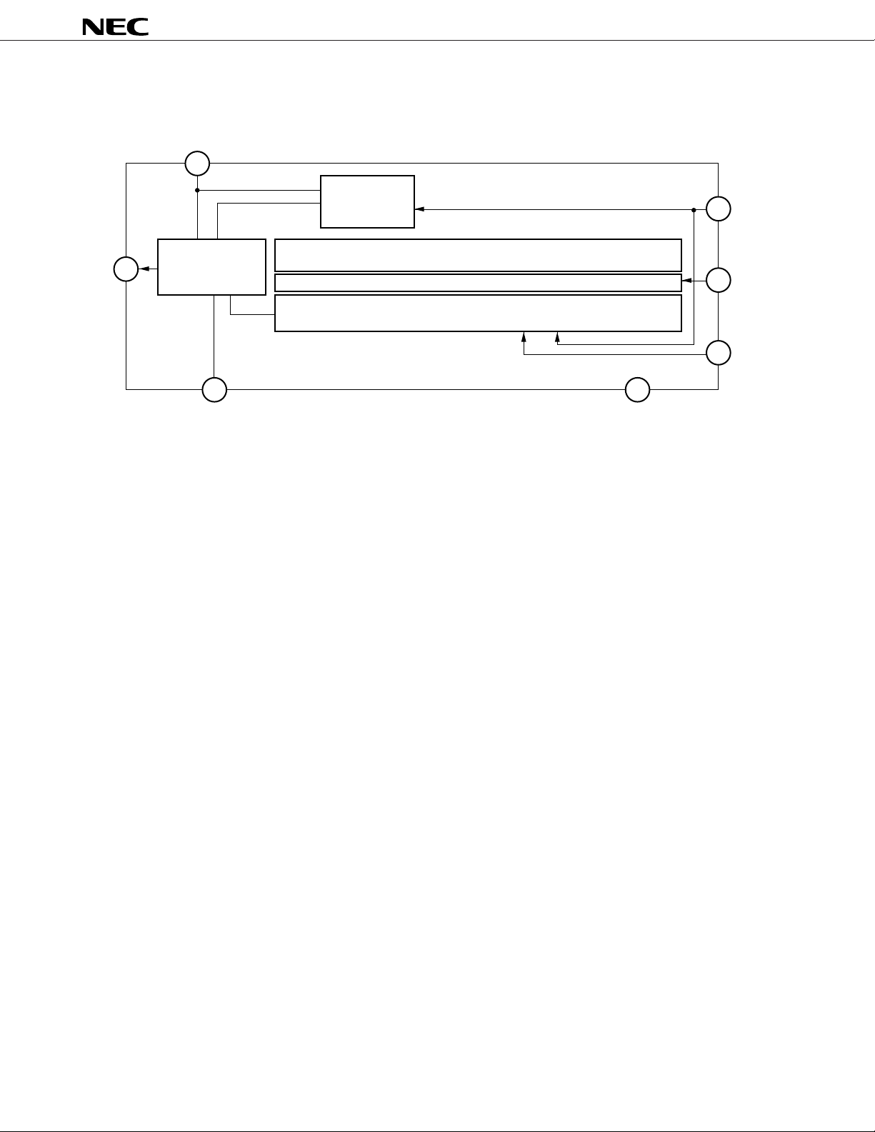
The µPD3753 is a 2088-bit high sensitivity CCD (Charge Coupled Device) linear image sensor which
changes optical images to electrical signal.
The µPD3753 consists of 2088-bit photocell array and a line of 2088-bit CCD charge transferred register.
It contains a reset a feed-through level clamp circuit, a pulse generator, and a voltage amplifier to provide
high sensitivity and low noise. It also supports low power consumption with single 5 V power supply. The
µ
PD3753 can be driven by power supply and three input clocks owing to the built-in reset pulse generator
and a clamp pulse generator.
FEATURES
• Valid photocell : 2088-bit
• Photocell's pitch : 14
• High response sensitivity : Providing a response equal with the existing equivalent NEC
• Low noise : Providing about two thirds register imbalance of the existing equivalent
• Peak response wavelength : 550 nm (green)
• Resolution : 8 dot/mm across the shorter side of a B4-size (257 × 364 mm) sheet
• Power supply : +5 V
• Drive clock level : CMOS output under +5 V operation
• Scanning speed : 1.0 ms/line
• Built-in circuit : Reset feed-through level clamp circuit, reset pulse generator, clamp pulse
ORDERING INFORMATION
Part Number Package Quality Grade
µ
PD3753CY CCD LINEAR IMAGE SENSOR 22 PIN PLASTIC DIP (400 mil) Standard
Please refer to "Quality grade on NEC Semiconductor Devices" (Document number IEI-1209) published by
NEC Corporation to know the specification of quality grade on the devices and its recommended applications.
µ
m
µ
product (
NEC product (µPD3743)
generator
PD3743) to the light from a daylight fluorescent lamp
Document No. IC-3429
(O. D. No. IC-9002)
Date Published August 1994 P
Printed in Japan
The information in this document is subject to change without notice.
©
1994
Page 2
BLOCK DIAGRAM
VOD
3
Reset pulse/
clamp pulse
generator
µ
PD3753
φ
2
15
VOUT
•Voltage amplifier
•Reset feed-through
19
level clamp circuit
Optical black (OB) 18 bits, invalid 2 bits,
valid photocell 2088 bits, invalid 2 bits
CCD register
20 13
AGND DGND
14
9
φ
TG
φ
1
2
Page 3
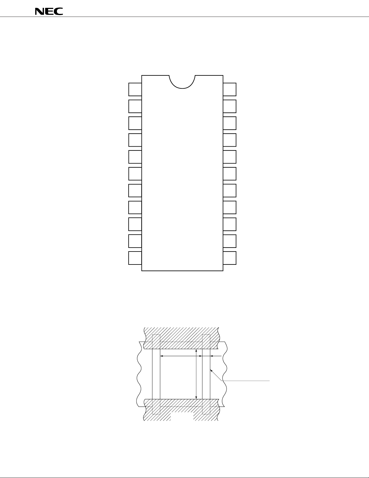
PIN CONFIGURATION (Top View)
CCD LINEAR IMAGE SENSOR 22 PIN PLASTIC DIP (400 mil)
µ
PD3753
No connection
No connection
Output unit drain voltage
No connection
No connection
No connection
No connection
No connection
Transfer gate clock
No connection
No connection
122
NC
221
NC
OD
320
V
419
NC
518
NC
617
NC
716
NC
815
NC
φ
914
TG
NC
10 13
11 12
NC NC
NC
NC
AGND
OUT
V
NC
NC
NC
φ
φ
DGND
2
1
No connection
No connection
Analog GND
Output
No connection
No connection
No connection
Shift register clock 2
Shift register clock 1
Digital GND
No connection
PHOTOCELL STRUCTURE DIAGRAM
12 m
µ
Aluminum
electrode
µ
14 m
2 m
µ
Channel stopper
3
Page 4
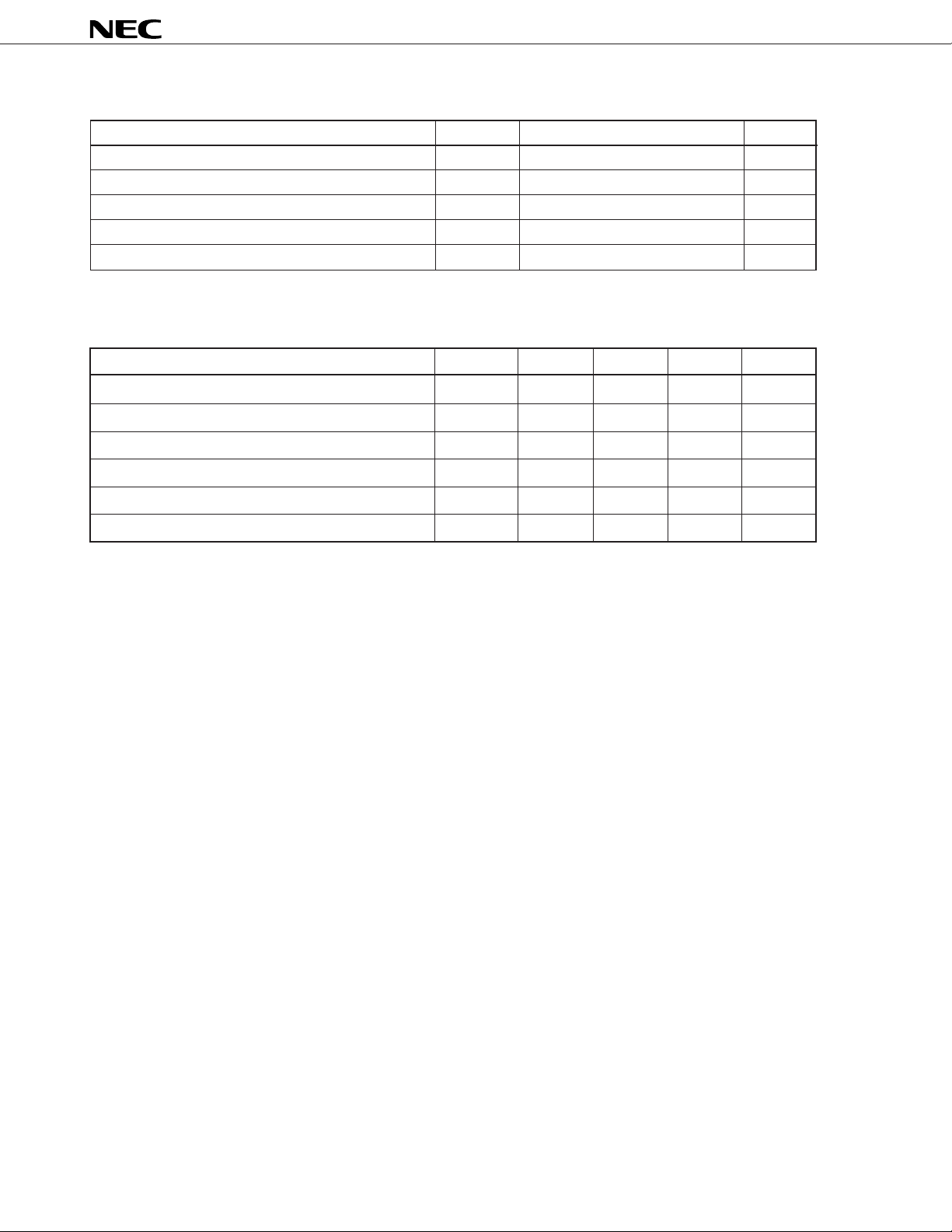
ABSOLUTE MAXIMUM RATINGS (Ta = +25 °C)
Parameter Symbol Ratings Unit
Output unit drain voltage VOD –0.3 to +8 V
Shift register clock voltage V
Transfer gate signal voltage V
φ
1, φ2 –0.3 to +8 V
φ
TG –0.3 to +8 V
Operating ambient temperature Topt –25 to +60 °C
Storage temperature Tstg –40 to +70 °C
RECOMMENDED OPERATING CONDITIONS (Ta = –25 to + 60 °C)
Parameter Symbol MIN. TYP. MAX. Unit
Output unit drain voltage VOD 4.7 5.0 5.3 V
µ
PD3753
Shift register clock φ1, φ2 signal high level V
Shift register clock φ1, φ2 signal low level V
Transfer gate signal high level V
Transfer gate signal low level V
Data rate f
Caution When V
φ
TGH > Vφ1H, image lag increases.
φ
1H, φ2H 4.5 5.0 VOD + 0.2 V
φ
1L, φ2L –0.3 0 +0.5 V
φ
TGH 4.5 Vφ1H Vφ1H V
φ
TGL –0.3 0 +0.5 V
φ
R 0.2 1 2 MHz
4
Page 5
µ
PD3753
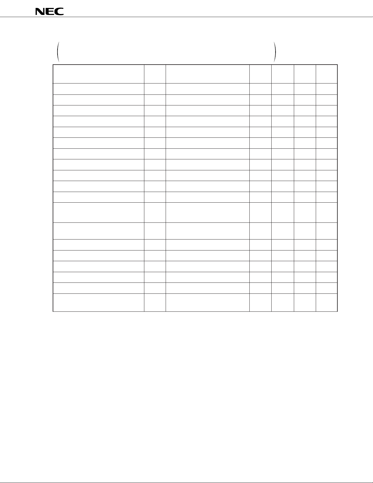
ELECTRICAL CHARACTERISTICS
Ta = +25 °C, VOD = 5 V, f
light source: 3200 K halogen lamp + C500 (infrared cut filter), input clock = 5 V
Parameter Symbol Test Conditions MIN. TYP. MAX. Unit
Saturation voltage Vsat 1.0 1.2 V
Saturation exposure SE Daylight color fluorescent lamp 0.013 lx•s
Photo response non-uniformity PRNU VOUT = 500 mV ± 2 ± 8 %
Average dark signal ADS Light shielding 1.0 8.0 mV
Dark signal non-uniformity DSNU Light shielding – 8 ± 4 + 8 mV
Power consumption PW 30 50 mW
Output impedance ZO 0.5 1 kΩ
Response RF Daylight color fluorescent lamp 63 90 117 V/lx•s
Response peak wavelength 550 nm
Image lag IL VOUT = 1 V 7 14 %
φ
1 = 1 MHz, data rate = 1 MHz, storage time = 10 ms
P-P
Offset level VOS 2.5 3.0 3.5 V
C
φ
Input capacitance of shift register
clock pin
Input capacitance of transfer gate
signal pin
Output fall delay time td 130 ns
Total transfer efficiency TTE VOUT = 1 V, data rate = 2 MHz 92 %
Dynamic range DR Vsat /DSNU 375 times
Reset feed-through noise RFSN Light shielding 0 800 1500 mV
Bit noise BN Light shielding 10 mVP-P
Resolution MTF 65 %
1
C
φ
2
C
φ
TG 100 pF
Modulation transfer function at
nyquist frequency
300 pF
Remark When VOD = 4.7 V, the response typically decreases to 90 % of the value under 5 V operation.
5
Page 6
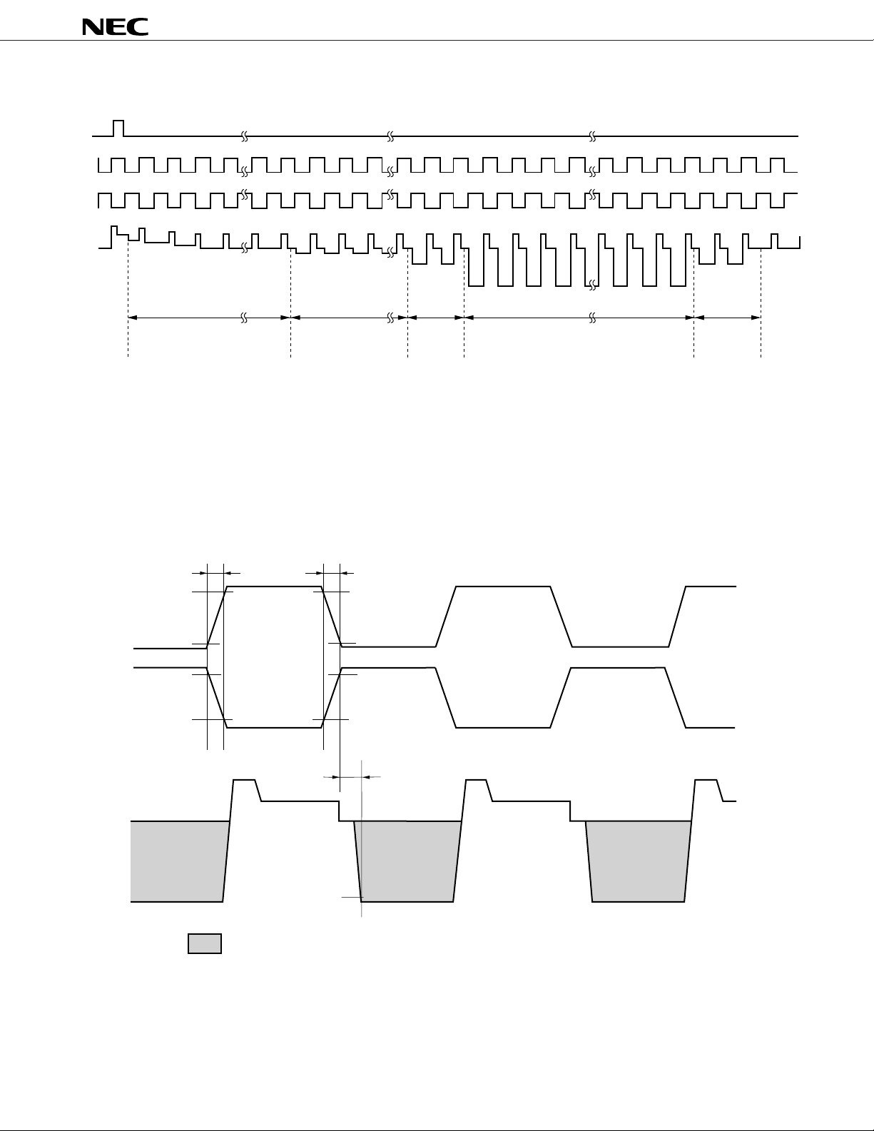
TIMING CHART 1
φ
TG
1
φ
1
φ
2
OUT
V
2
µ
PD3753
3
4
5
12
13
14
15
16
31
32
33
34
35
36
37
2118
2119
2120
2121
2122
2123
2124
V
OUT
unstable period
12 bits*
Caution Be sure not to use this period (indicated by *) as the black level, because this part is unstable.
TIMING CHART 2
t1
90%
φ
1
10%
90%
OB (Optical black)
18 bits
t2
90%
10%
90%
Invalid
photocell
2 bits
Valid photocell 2088 bits
Invalid
photocell
2 bits
φ
2
10%
10%
td
V
OUT
10%
Remark : Signal output
6
Page 7
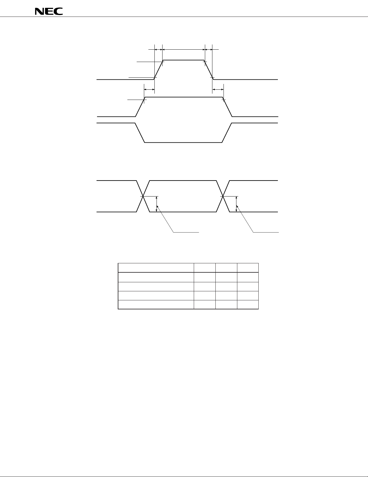
TIMING CHART for φTG, φ1, φ2
φ
TG
90 %
10 %
t5t3 t4
µ
PD3753
t6
90 %
1
φ
2
φ
7
t
CROSS POINTS for φ1, φ2
1
φ
2
φ
Note Adjust cross point of φ1, φ2 by φ1, φ2 pin external input resistors.
(Unit: ns)
Parameter MIN. TYP. MAX.
t1 ,t2 0 50 (100)
t3, t4 0 50 –
t5 650 1000 (2000)
t6, t7 0 100 –
2 V or more2 V or more
Remark The MAX. in the table above shows the operation range in which the output characteristics are kept
µ
almost enough for general purpose, does not show the limit above which the
PD3753 is destroyed.
7
Page 8
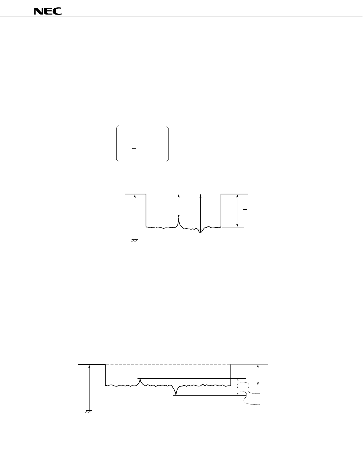
DEFINITIONS OF CHARACTERISTIC ITEMS
1. Saturation voltage: Vsat
Output signal voltage at which the response linearity is lost.
2. Saturation exposure: SE
Product of intensity of illumination (lx) and storage time (s) when saturation of output voltage occurs.
3. Photo response non-uniformity: PRNU
The peak/bottom ratio to the average output voltage of all the valid bits calculated by the following formula.
µ
PD3753
VMAX. or VMIN.
PRNU (%) =
Register Dark
DC level
4. Average dark signal: ADS
Output average voltage in light shielding.
n
ADS(mV) =
1
∑
n
j=1
n
1
∑
n
j=1
V
j
–1
V
j
x 100
V MIN.
n : Number of valid bits
j : Output voltage of each bit
V
n
1
V
j
∑
V MAX.
n
j=1
5. Dark signal non-uniformity: DSNU
The difference between peak or bottom output voltage in light shielding and ADS.
Register Dark
DC level
8
ADS
DSNU MIN.
DSNU MAX.
Page 9
µ
PD3753
6. Output impedance: Z
o
Output pin impedance viewed from outside.
7. Response: R
Output voltage divided by exposure (lx
•s).
Note that the response varies with the light source.
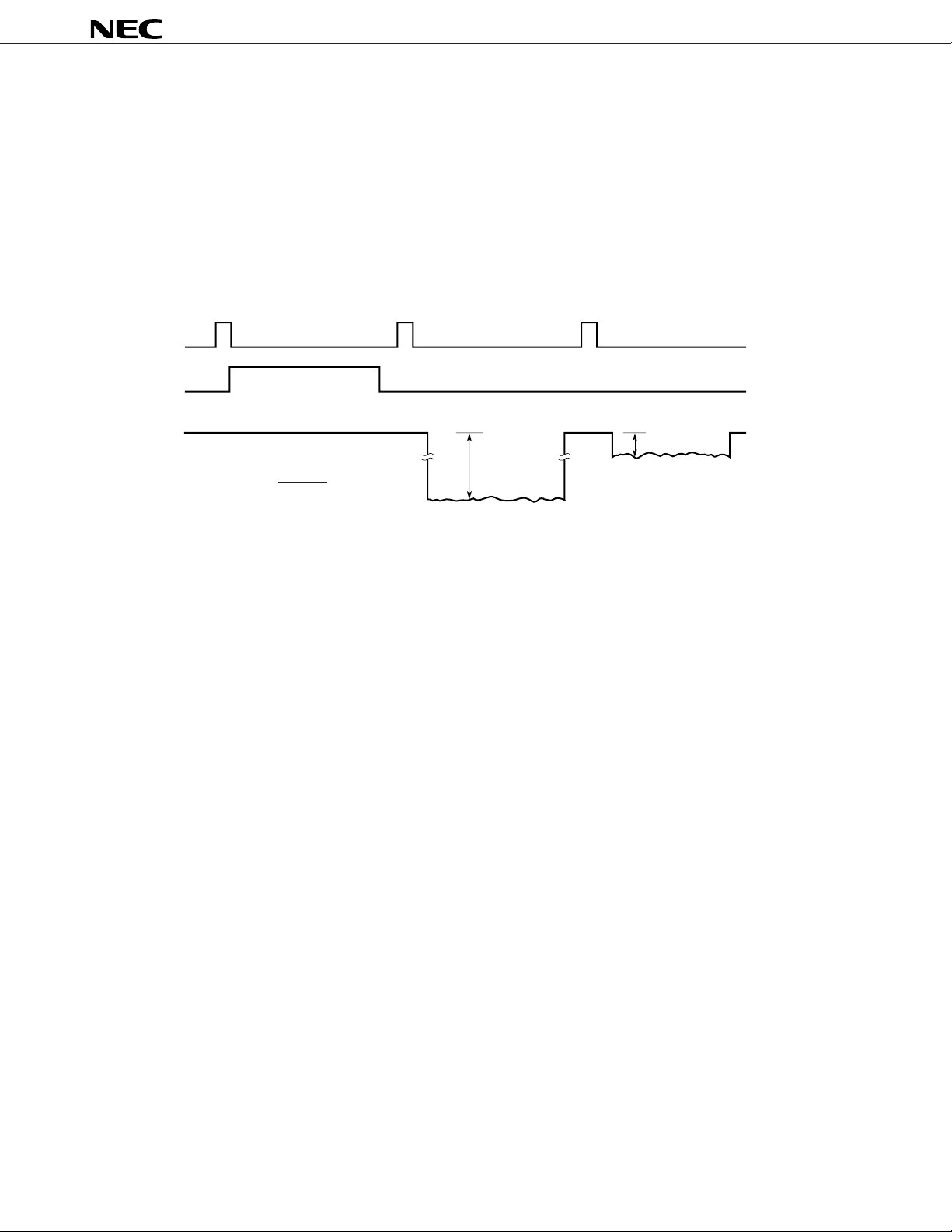
8. Image Lag: IL
The rate between the last output voltage and the next one after read out the data of a line.
TG
φ
Light
V
OUT
IL =
ON
V1
× 100 (%)
V
OUT
OFF
V
1
VOUT
9. Bit Noise: BN
Output signal distribution of a photocell by scan.
9
Page 10
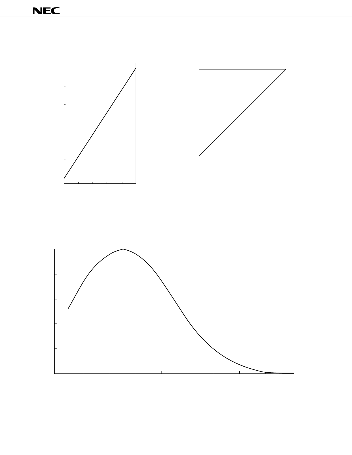
STANDARD CHARACTERISTIC CURVES (Ta = +25 °C)
DARK OUTPUT TEMPERATURE
CHARACTERISTIC
8
4
2
1
0.5
Relative Output Voltage
0.25
STORAGE TIME OUTPUT VOLTAGE
CHARACTERISTIC
2
1
Relative Output Voltage
0.2
µ
PD3753
0.1
01020304050
Ambient Temperature T ( C)
100
80
60
40
Response Ratio (%)
0.1
°
a
SPECTRAL RESPONSE CHARACTERISTIC
5101
Storage Time (ms)
10
20
0
1200600400 1000800
Wavelength (nm)
Page 11
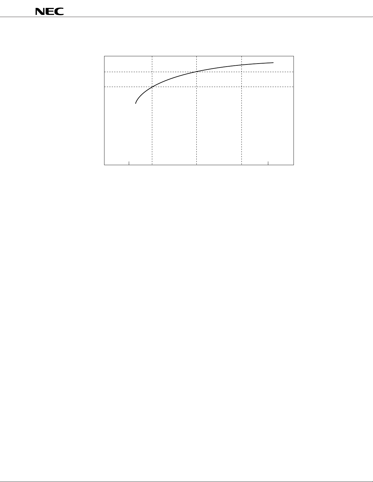
POWER SUPPLY VOLTAGE RESPONSE RATIO CHARACTERISTIC
110
100
90
Response Ratio (%)
µ
PD3753
0
4.74.5 5.0 5.3 5.5
Power Supply Voltage (V)
11
Page 12
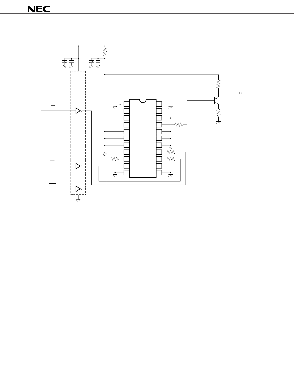
APPLICATION EXAMPLE
µ
PD3753
10 F
µ
/16 V
PD74HC04
µ
2
φ
1
φ
µ
0.1 F
µ
+5 V
10 Ω
10 Ω
+5 V
0.1 F
++
10 F
µ
/16 V
1
2
3
4
5
6
7
8
9
10
11
PD3753CY
µ
NC
NC
VOD
NC
NC
NC
NC
NC
TG
φ
NC
NC
NC
NC
AGND
VOUT
NC
NC
NC
φ
1
φ
DGND
NC
2.2 kΩ
VOUT
22
21
20
19
18
17
16
15
2
14
13
12
100 Ω
47 Ω
47 Ω
2SA1005
100 Ω
TG
φ
The application circuits and their parameters are for references only and are not intended for use in actual design-in's.
12
Page 13
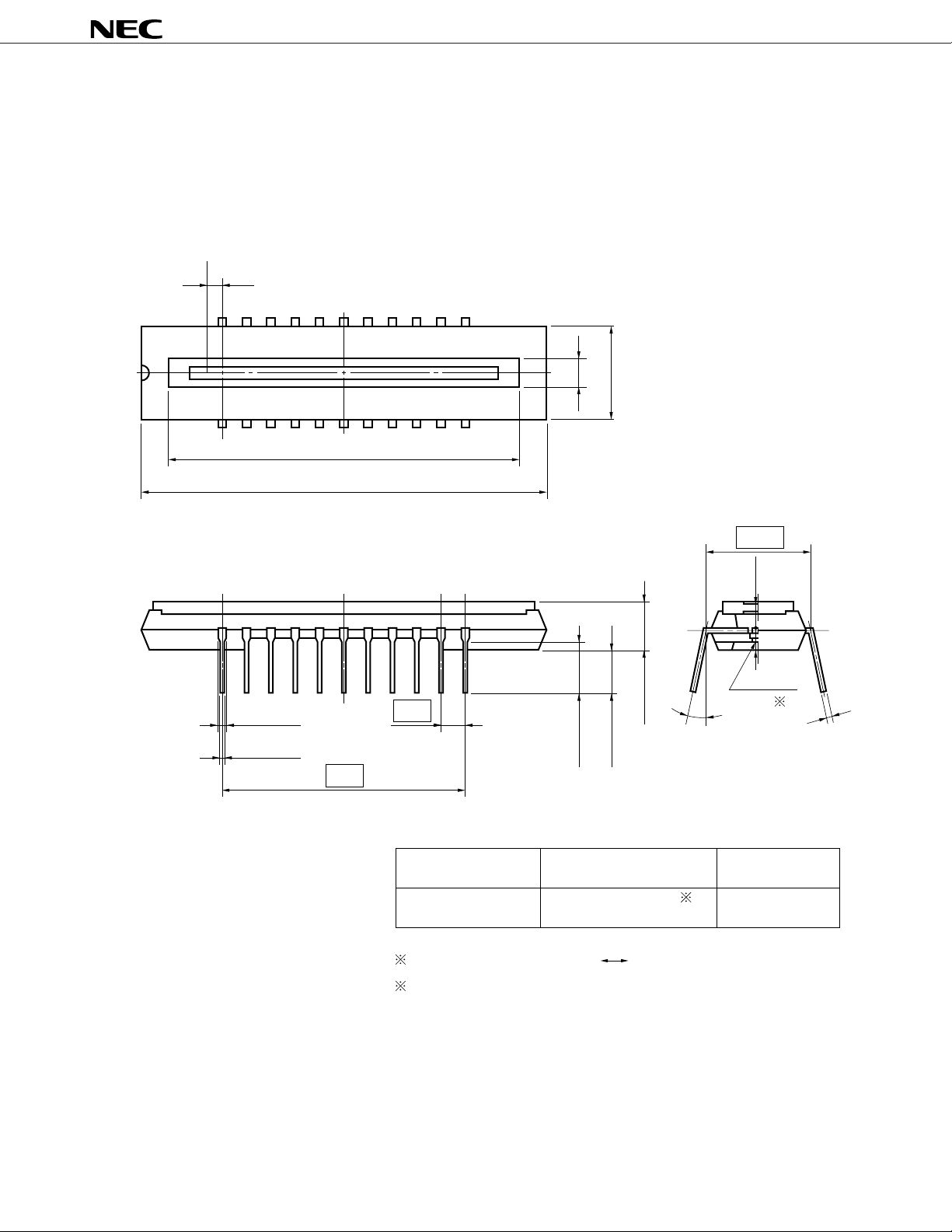
PACKAGE DIMENSIONS
CCD LINEAR IMAGE SENSOR 22PIN PLASTIC DIP (400 mil)
(Unit : mm)
1bit
1.7±0.3
2.0
37.5
9.25±0.3
µ
PD3753
1.02±0.15
0.46±0.1
44.0±0.3
25.4
2.54
4.21±0.5
(5.42)
Name Dimensions
Plastic cap
42.9 × 8.35 × 0.7
4.39±0.4
0~10°
10.16
(1.99)
2.35±0.2
Refractive index
2
1
0.25±0.05
1.5
1
The bottom of the package The surface of the chip
The thickness of the cap over the chip
2
22C-1CCD-PKG2
13
Page 14

RECOMMENDED SOLDERING CONDITIONS
The following conditions (see table below) must be met when soldering this product.
For more details, refer to our document “SEMICONDUCTOR DEVICE MOUNTING TECHNOLOGY MANUAL”
(IEI-1207).
Please consult with our sales offices in case other soldering process is used, or in case soldering is done
under different conditions.
Table 1 Type of Through Hole Device
µ
PD3753CY: CCD LINEAR IMAGE SENSOR 22 PIN PLASTIC DIP (400 mil)
Soldering Process Soldering Conditions
Wave soldering (Only lead part) Solder temperature: 260 °C or below,
Flow time: 10 seconds or below
Partial heating method Pin temperature: 260 °C or below,
Time: 10 seconds or below
Caution Do not jet molten solder on the surface of package.
µ
PD3753
14
Page 15
NOTES FOR CMOS DEVICES
1 PRECAUTION AGAINST ESD FOR SEMICONDUCTORS
Note: Strong electric field, when exposed to a MOS device, can cause destruction of
the gate oxide and ultimately degrade the device operation. Steps must be
taken to stop generation of static electricity as much as possible, and quickly
dissipate it once, when it has occurred. Environmental control must be
adequate. When it is dry, humidifier should be used. It is recommended to
avoid using insulators that easily build static electricity. Semiconductor
devices must be stored and transported in an anti-static container, static
shielding bag or conductive material. All test and measurement tools including
work bench and floor should be grounded. The operator should be grounded
using wrist strap. Semiconductor devices must not be touched with bare
hands. Similar precautions need to be taken for PW boards with semiconductor
devices on it.
µ
PD3753
2 HANDLING OF UNUSED INPUT PINS FOR CMOS
Note: No connection for CMOS device inputs can be cause of malfunction. If no
connection is provided to the input pins, it is possible that an internal input
level may be generated due to noise, etc., hence causing malfunction. CMOS
devices behave differently than Bipolar or NMOS devices. Input levels of CMOS
devices must be fixed high or low by using a pull-up or pull-down circuitry. Each
unused pin should be connected to VDD or GND with a resistor, if it is considered
to have a possibility of being an output pin. All handling related to the unused
pins must be judged device by device and related specifications governing the
devices.
3 STATUS BEFORE INITIALIZATION OF MOS DEVICES
Note: Power-on does not necessarily define initial status of MOS device. Production
process of MOS does not define the initial operation status of the device.
Immediately after the power source is turned ON, the devices with reset
function have not yet been initialized. Hence, power-on does not guarantee
out-pin levels, I/O settings or contents of registers. Device is not initialized
until the reset signal is received. Reset operation must be executed immedi-
ately after power-on for devices having reset function.
15
Page 16

[MEMO]
µ
PD3753
No part of this document may be copied or reproduced in any form or by any means without the prior written
consent of NEC Corporation. NEC Corporation assumes no responsibility for any errors which may appear in this
document.
NEC Corporation does not assume any liability for infringement of patents, copyrights or other intellectual
property rights of third parties by or arising from use of a device described herein or any other liability arising
from use of such device. No license, either express, implied or otherwise, is granted under any patents,
copyrights or other intellectual property rights of NEC Corporation or others.
The devices listed in this document are not suitable for use in aerospace equipment, submarine cables, nuclear
reactor control systems and life support systems. If customers intend to use NEC devices for above applications
or they intend to use "Standard" quality grade NEC devices for applications not intended by NEC, please contact
our sales people in advance.
Application examples recommended by NEC Corporation
Standard: Computer, Office equipment, Communication equipment, Test and Measurement equipment,
Machine tools, Industrial robots, Audio and Visual equipment, Other consumer products, etc.
Special: Automotive and Transportation equipment, Traffic control systems, Antidisaster systems, Anticrime
systems, etc.
M4 92.6
 Loading...