NEC UPD16855AG, UPD16855DG, UPD16855CG, UPD16855BG, UPD16855BC Datasheet

DATA SHEET
MOS INTEGRATED CIRCUIT
µµµµ
PD16855A/B/C/D
DUAL HIGH-SIDE SWITCH FOR USB APPLICATION
DESCRIPTION
This product is the power switch IC with over current limit, used for the power supply bus of the Universal-Serial-
Bus (USB).
2 circuit builds in the Pch power MOSFET in the switch part, and this product realizes low on resistance (100 m
TYP.) respectively.
And the over current detection, the thermal-shutdown circuit, an under voltage locked-out (UVLO) circuit whose
functions are necessary in the Host/HUB-controller of the USB standard are built in.
And the over-current-detect result can be reported to the controller by flag-pin.
This product builds in each two circuits of the power switch, control-pins and flag-pins, and this IC can be able to
control the power supply bus in 2 USB port.
There are four kinds of this product by the input logic of the control signal and switch operation in over-current
detect.
Ω
FEATURES
•Pch power MOSFET, 2 circuit building in
•Over-current detection circuit is built in and its result is outputted from flag-pin (“L” active)
•Prevent from dropping power supply by over current limit circuit
•Thermal shutdown circuit building in
•Under Voltage Locked Out (UVLO) circuit building in
•Switch on/off control is possible by the control-pin.
•8 pin DIP/SOP package
ORDERING INFORMATION
PART NO. PACKAGE
PD16855BC 8-pin plastic DIP (300mil)
µ
PD16855AG 8-pin plastic SOP (225mil)
µ
PD16855BG 8-pin plastic SOP (225mil)
µ
PD16855CG 8-pin plastic SOP (225mil)
µ
PD16855DG 8-pin plastic SOP (225mil)
µ
The information in this document is subject to change without notice. Before using this document, please
confirm that this is the latest version.
Not all devices/types available in every country. Please check with local NEC representative for
availability and additional information.
Document No. S13020EJ1V0DS00 (1st edition)
Date Published February 1999 N CP(K)
Printed in Japan
1998©

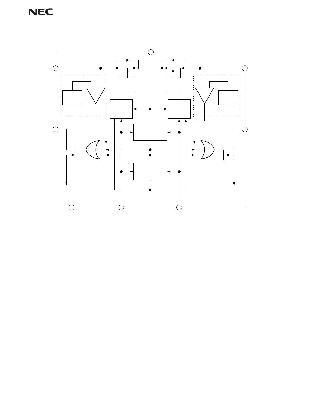
BLOCK DIAGRAM
IN (Input)
7
µµµµ
PD16855
OUT1
(Output1)
FLG1
(Flag Out1)
8
2
Ref.
Voltage
Over Current
Detect
6
GND
Gate
Control
1
CTL1
(Control Input1)
UVLO
Thermal
Shutdown
Gate
Control
4
CTL2
(Control Input2)
Ref.
Voltage
Over Current
Detect
5
OUT2
(Output2)
3
FLG2
(Flag Out2)
The internal resister doesn’t connect to input terminal of CTL1 (1 pin) and CTL2 (4 pin).
Note
Therefore the input level must be “H” or “L” even if these pins aren’t used.
2
Data Sheet S13020EJ1V0DS00

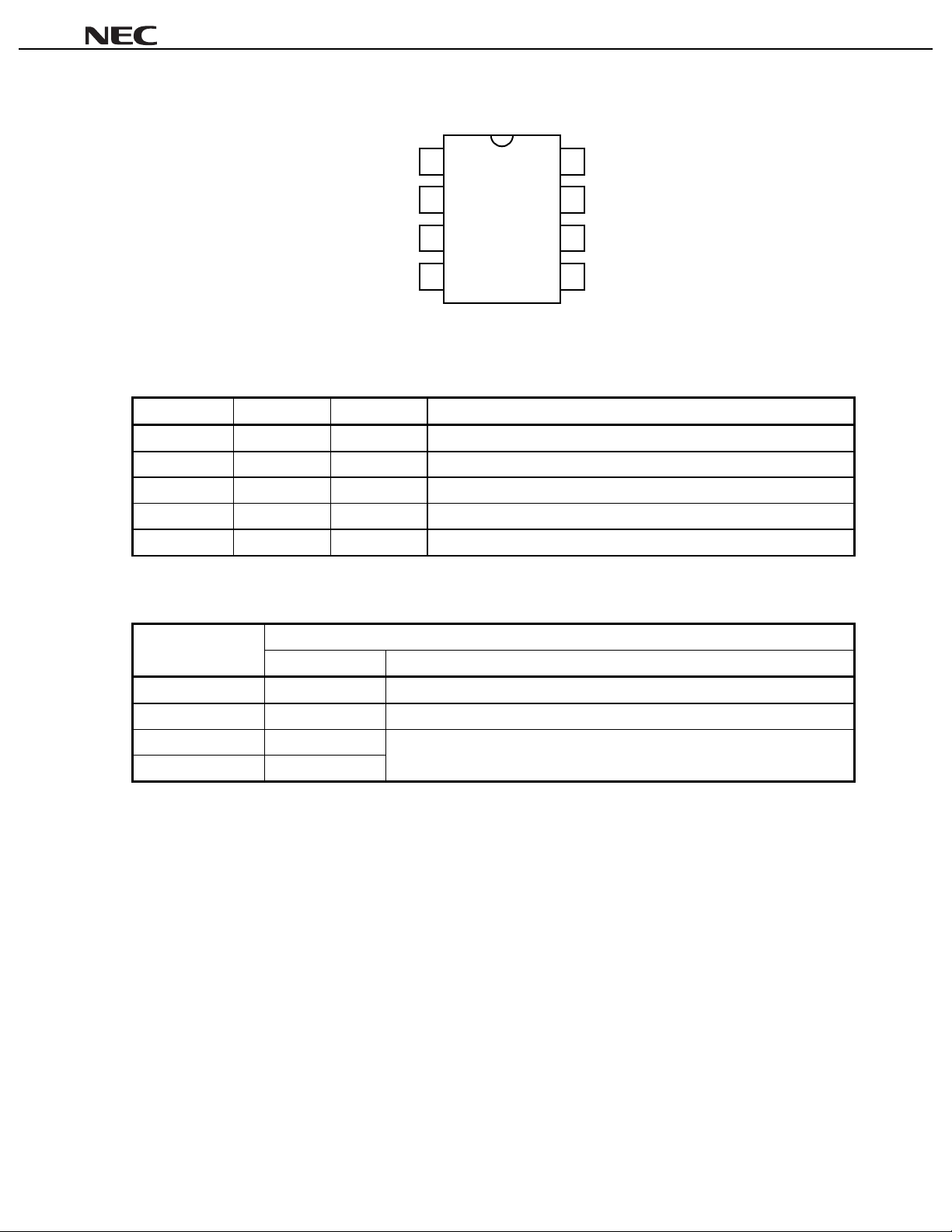
CONNECTION DIAGRAM (TOP VIEW)
1CTL1 OUT18
2FLG1 IN7
3FLG2 GND6
4CTL2 OUT25
8-Pin DIP/SOP
PIN CONFIGURATION
PIN No. SYMBOL I/O FUNCTION
1/4 CTL1/CTL2 Input Control : TTL Input
2/3 FLG1/FLG2 Output Over Current Detect Flag : Ac tive-L, Nch open-drain
6 GND Power G round
7 IN Power (Input) Power Supply : Source of MO S F ET
8/5 OUT1/OUT2 Output Output of Switch : Drain of MOSFET
µµµµ
PD16855
DESCRIPTION of
PART No.
PD16855AG “H” active Over-Current Limit Operation. Switch Off with CTL Input “L”
µ
PD16855BC/BG “L” active Over-Current Lim i t Operation. Switch Off wit h CTL Input “H”
µ
PD16855CG “H” active
µ
PD16855DG “L” active
µ
PD16855A/B/C/D FUNCTION
µµµµ
Abstract of Functi on
CTL Input Logic Switch Operation with Over-Current Detect
Switch Off regardless of CTL Input
Data Sheet S13020EJ1V0DS00
3

µµµµ
PD16855
PIN CONFIGURATION
PD16855AG (Active-H)
µµµµ
CTL1 FLG1 OUT1 CTL2 FLG2 OUT2 Operating mode
H H ON H H ON normal mode
H H ON L H OFF only OUT1 is ON
L H OFF H H ON only OUT2 is ON
L H OFF L H OFF st andby m ode
H L ON H H ON only OUT1 is over-current detect
H H ON H L ON only OUT2 is over-current detect
X L OFF X L OFF TSD mode
X L OFF X L OFF UVLO mode
PD16855BC/BG (Active-L)
µµµµ
CTL1 FLG1 OUT1 CTL2 FLG2 OUT2 Operating mode
L H ON L H ON normal mode
L H ON H H OFF only OUT1 is ON
H H OFF L H ON only OUT2 is ON
H H OFF H H OFF standby mode
L L ON L H ON only OUT1 is over-current detect
L H ON L L ON only OUT2 is over-current detect
X L OFF X L OFF TSD mode
X L OFF X L OFF UVLO mode
(H:Hi-level, L:Low-level, ON:output ON state, OFF:output OFF state, X:H or L)
4
Data Sheet S13020EJ1V0DS00

PD16855CG (Active-H and Switch off with over-current detect)
µµµµ
CTL1 FLG1 OUT1 CTL2 FLG2 OUT2 Operating mode
H H ON H H ON normal mode
H H ON L H OFF only OUT1 is ON
L H OFF H H ON only OUT2 is ON
L H OFF L H OFF st andby m ode
H L OFF H H ON only OUT1 is over-current detect
H H ON H L OFF only OUT2 is over-current detect
X L OFF X L OFF TSD mode
X L OFF X L OFF UVLO mode
PD16855DG (Active-L and Switch off with over-current detect)
µµµµ
CTL1 FLG1 OUT1 CTL2 FLG2 OUT2 Operating mode
L H ON L H ON normal mode
L H ON H H OFF only OUT1 is ON
H H OFF L H ON only OUT2 is ON
H H OFF H H OFF standby mode
L L OFF L H ON only OUT1 is over-current detect
L H ON L L OFF only OUT2 is over-current detect
X L OFF X L OFF TSD mode
X L OFF X L OFF UVLO mode
µµµµ
PD16855
Data Sheet S13020EJ1V0DS00
5

µµµµ
PD16855
ABSOLUTE MAXIMUM RATINGS (TA = 25
Parameter Symbol Conditions Ratings Unit
Input Voltage V
Flag Voltage V
Flag Current I
Output Voltage V
Output Current I
Control Input Voltage V
DIP 400Power Dissipation
SOP
Operating Temperature Range T
Channel Temperature Range T
Storage Temperature Range T
The thermal shutdown circuit (operating temperature is more than 150 °C typ.) builds in this product.
Note
IN
FLG
FLG
OUT
OUT
CTL
D
P
A
CH MAX
stg
C)
°°°°
DC +0.5(VIN = V
Pulse Width ≤ 100µs
Single Pulse
–0.3 to +6 V
–0.3 to +6 V
50 mA
VIN + 0.3 V
CTL
=5 V)
–0.1 (V
IN
= 0V, V
OUT
= 5V)
+3
–0.3 to +6 V
300
–40 to +85 °C
+150 °C
–55 to +150 °C
A
mW
RECOMMENDED OPERATING RANGE
Parameter Symbol Min Typ Max Unit
Input Voltage V
Operating Temperature Range T
IN
A
+4 +5.5 V
0+70°C
6
Data Sheet S13020EJ1V0DS00

ELECTRICAL CHARACTERISTICS
DC CHARACTERISTICS (Unless otherwise specified, V
Parameter Symbol Conditions Min Typ Max Unit
IN
= +5V; TA = +25°C)
µµµµ
PD16855
PD16855A/C)
(only
µ
PD16855B/D)
(only
µ
Low-level Input Voltage V
High-level Input Voltage V
Output Leak Current I
O LEAK
Over Current Detect Threshold I
Flag Output Resistance R
Flag Leak Current I
Operating Voltage of
O LEAK F
V
Under Voltage Locked Out
Circuit
DD
I
DD
I
IL
IH
CTL
ON
TH
ON F
UVLO
CTL
V
= 0V (both 1 pin & 4 pin),
15
µ
OUT = open
CTL
V
= VIN, OUT = open 1 1.5 mA
CTL
V
= VIN (both 1 pin & 4 pin),
15
µ
OUT = open
CTL
V
= 0V, OUT = open 1 1.5 mA
CTL Pin 1.0 V
CTL Pin 2.0 V
CTL
V
= 0V 0.01 1
CTL
IN
V
= V
TA = 0 to +70 °C,
OUT
= 500 mA
I
DIP 100 140Output MOSFET On Resis tance R
SOP 100 130
0.01 1
10
µ
µ
m
µ
TA = 0 to +70 °C 0.6 0.9 1.25 A
IL = 10 mA 10 25
FLAG
V
= 5 V 0.01 1
µ
VIN : Up 3.2 3.5 3.7 V
VIN : Down 3.0 3.3 3.5 V
Hysteresis 0.1 0.2 0.3 V
ACircuit Current
ACircuit Current
AInput Current of CTL pin I
A
Ω
A
Ω
A
AC CHARACTERISTICS (Unless otherwise specified, VIN = +5 V; TA = +25
Parameter Symbol Conditions Min Typ Max Unit
Output Transition
Rising Time
Output Transition
Falling Time
Over Current Detect
Delay Time
CTL Input Low-Level Time
PD16855A/C)
(only
µ
CTL Input High-Level Time
PD16855B/D)
(only
µ
RISE
t
FALL
t
OVER
t
t
t
CTL
CTL
RL = 10 Ω each output 2.5 12 ms
RL = 10 Ω each output 10
520
CTL : H→L→H20
CTL : L→H→L20
C)
°°°°
s
µ
s
µ
s
µ
s
µ
Data Sheet S13020EJ1V0DS00
7

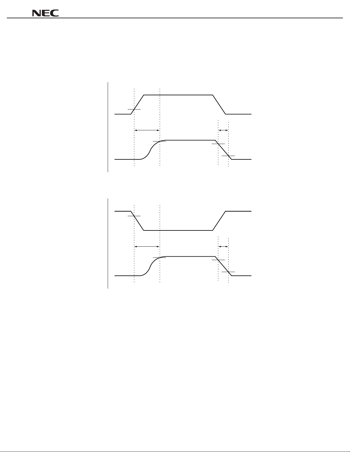
MEASUREMENT POINT
Output Transition Rising Time (at ON)/Output Transition Falling Time (at OFF)
at the timing of CTL changing “L” to “H”/“H” to “L” for µPD16855A/C
5 V/3.3 V
µµµµ
PD16855
CTL
OUT
V
0 V
5 V
0 V
10%
t
RISE
90% 90%
at the timing of CTL changing “H” to “L”/“L” to “H” for µPD16855A/C
5 V/3.3 V
0 V
5 V
0 V
90%
t
RISE
90% 90%
CTL
OUT
V
t
FALL
t
FALL
10%
10%
8
Data Sheet S13020EJ1V0DS00

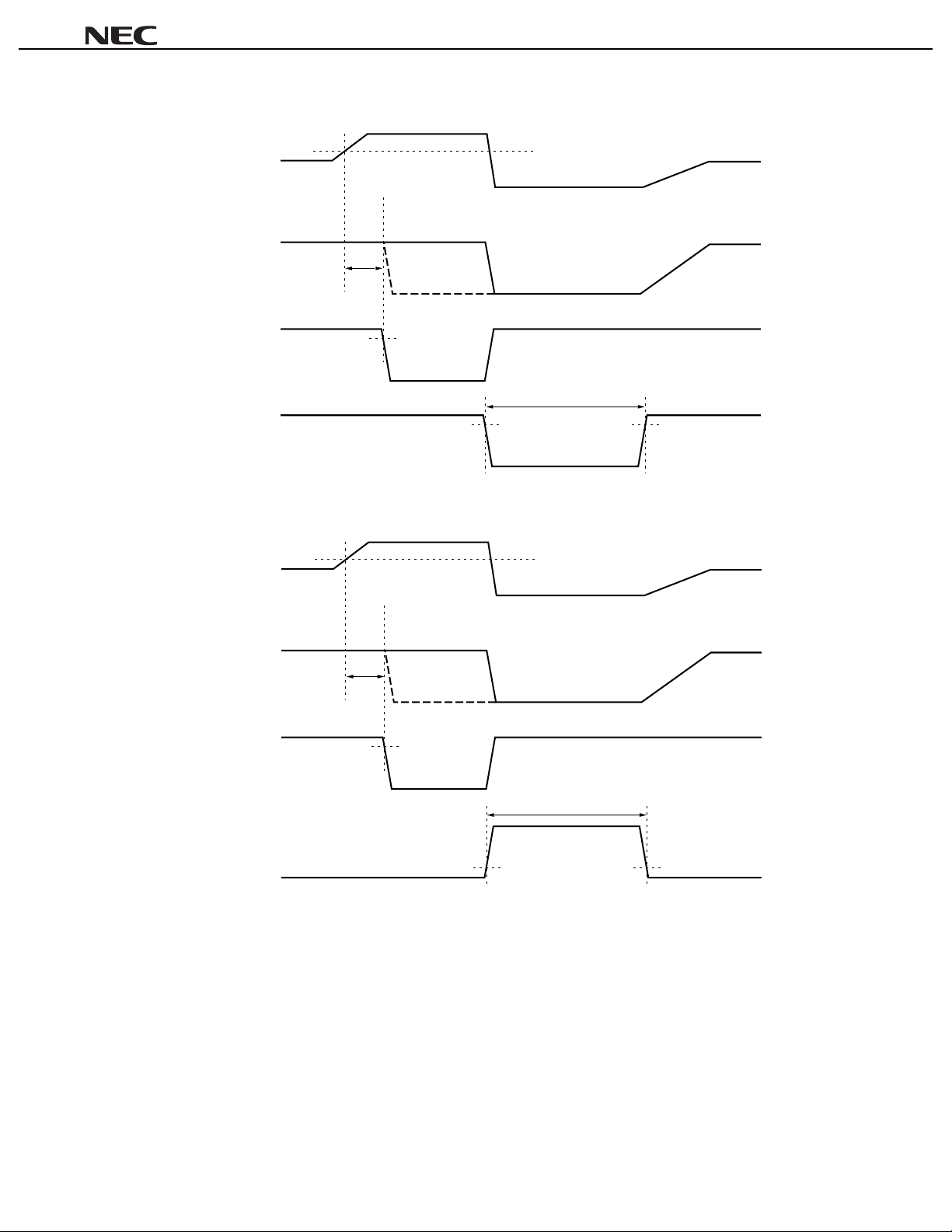
Over Current Detect Delay Time/CTL Input Low-Level Time for µPD16855A/C
µµµµ
PD16855
IOUT
VOUT
FLG
CTL
tOVER
µ
PD16855A
PD16855C
µ
90%
90% 90%
ITH
tCTL
Over Current Detect Delay Time/CTL Input High-Level Time for µPD16855B/D
I
OUT
ITH
V
OUT
FLG
CTL
t
OVER
PD16855B
µ
PD16855D
µ
90%
t
CTL
10% 10%
Data Sheet S13020EJ1V0DS00
9
 Loading...