NEC UPD16431AGC-7ET Datasheet

DATA SHEET
MOS INTEGRATED CIRCUIT
µ
PD16431A
1/2, 1/3, 1/4-DUTY LCD CONTROLLER/DRIVER
The µPD16431A is an LCD controller/driver that enables display of segment type LCDs of 1/2, 1/3, or 1/4 duty
cycle. This controller/driver has 56 segment output lines of which eight can also be used as LED output lines.
µ
Because the LCD driver contained in the
drive voltage can be set. In addition, key source output lines for key scanning and key input data lines are
µ
also provided, so that the
FEATURES
• Various display modes
1/2 duty: 112 segment outputs or 96 segment outputs + 8 LED outputs
1/3 duty: 168 segment outputs or 144 segment outputs + 8 LED outputs
1/4 duty: 224 segment outputs or 192 segment outputs + 8 LED outputs
• Key scan circuit (key source outputs are shared with LCD driver outputs)
• Independent LCD driver power supply V
• Serial data input/output (SCK, STB, DATA)
• On-chip oscillator incorporated
• Power-ON reset circuit
PD16431A is ideal for applications in the front panel of an automobile stereo system.
PD16431A has separate logic and power supply, up to 6.5 V of LCD
LCD (can be set to VDD to 6.5 V)
ORDERING INFORMATION
Part Number Package
µ
PD16431AGC-7ET 80-pin plastic QFP (0.65 pitch, 14 × 14)
Document No. IC-3414
(O.D. No. IC-8885)
Date Published January 1995 P
Printed in Japan
©
1995
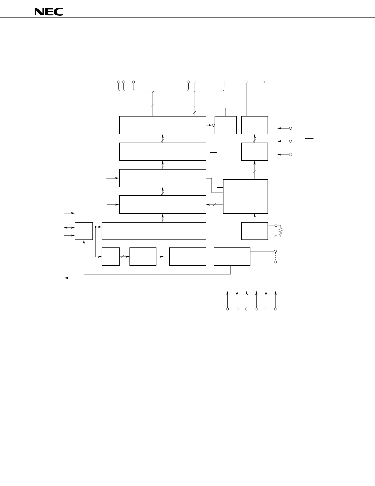
BLOCK DIAGRAM
µ
PD16431A
STB
DATA
CLK
Key counter
Write address
I/O
control
8-bit
shift
register
1
2
8
/KS
/KS
/KS
1
1
8
S
S
S
Level shifter (56)
Output latch (56 × 4)
56-bit shift register
Command
decoder
8
48
Segment driver
56
56
Selector circuit
56
56
Key counter
48
S
1
/LED
49
S
8
8
OE
LED
driver
2
Read
address
Key latch S/R
8
/LED
56
S
COM1COM
Common
driver
Level
shifter
Timing
generator
OSC
4
OE
4
LCD/LED
SYNC
4
OSC
IN
OSC
OUT
key
1
key
4
KEY REQ
VDDVSSV
LCDVLC1VLC2VLC3
2
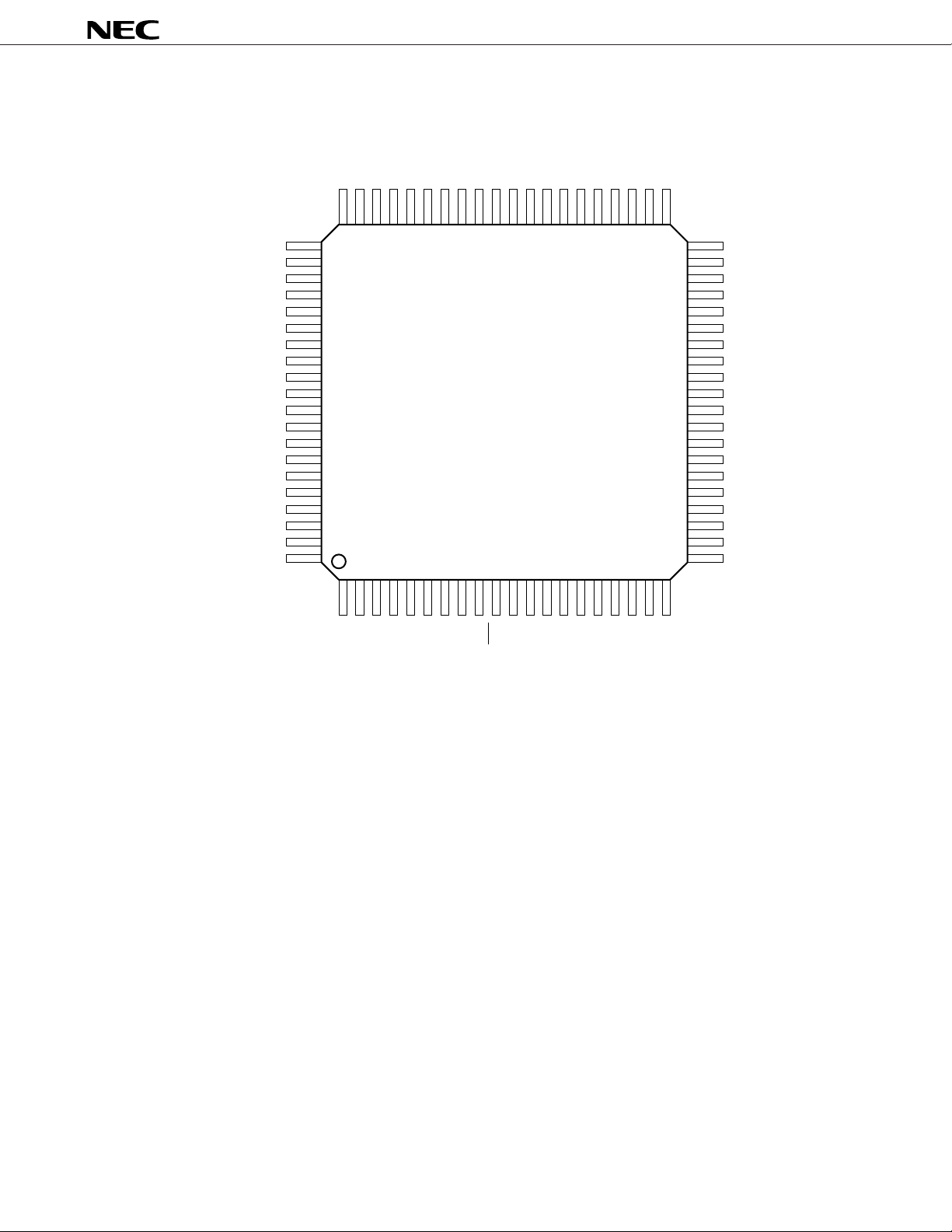
PIN CONFIGURATION
µ
PD16431A
SEG36
SEG35
SEG34
SEG33
SEG32
SEG31
SEG30
SEG29
SEG28
SEG27
SEG26
SEG25
SEG24
SEG23
SEG22
SEG21
SEG20
SEG19
SEG18
SEG17
SEG37
SEG38
SEG39
SEG40
SEG41
SEG42
SEG43
SEG44
SEG45
SEG46
SEG47
SEG48
SEG49/LED1
SEG50/LED2
SEG51/LED3
SEG52/LED4
SEG53/LED5
SEG54/LED6
SEG55/LED7
SEG56/LED8
61
80
4160
40
21
201
VSS
KEY1
KEY2
KEY3
KEY4
KEY REQ
SCK
STB
DATA
IN
OE
OSC
LCD/LED
OSCOUT
DD
V
SYNC
VLCD
VLC1
VLC2
VLC3
VEE
SEG16
SEG15
SEG14
SEG13
SEG12
SEG11
SEG10
SEG9
SEG8/KS8
SEG7/KS7
SEG6/KS6
SEG5/KS5
SEG4/KS4
SEG3/KS3
SEG2/KS2
SEG1/KS1
COM4
COM3
COM2
COM1
Note Though VSS and VEE are internally connected, be sure to connect all the power supply pins (VDD, VSS,
VLCD, and VEE).
3

PIN FUNCTIONS
µ
PD16431A
Symbol
SEG1/KS1 to
SEG8/KS8
SEG9 to SEG48
SEG49/LED1 to
SEG56/LED8
COM1 to COM4
SCK
DATA
STB
LCD/LED
Note
OE
Name
Segment output/key
source output
Segment output
Segment output/LED
output pins
Common output
Shift clock input
Data input/output
Strobe input
LCD/LED select
Output enable input
No.
25 to 32
33 to 72
73 to 80
21 to 24
7
8
9
10
11
Description
These pins serve as LCD segment output pins and key
source output pins for key scanning.
LCD segment output pins
These pins can be used as LCD segment output or LED
output pins depending on the setting of the LCD/LED pin.
LCD common output pins
Data shift clock. Data is read at the rising edge, and is
output at the falling edge of this clock.
This pin inputs a command or display data, or outputs
key data.
A command or data is input at the rising edge of the shift
clock, starting from the most significant bit. Key data is
output at the falling edge of the shift clock, starting from
the most significant bit.
This pin serves as an open-drain pin in the output mode.
Data can be input when this signal goes low. When it
goes high, command processing is performed.
When this signal goes high, the SEGn/LEDm pins function
as LCD segment output pins; when it goes low, they
function as LED driver output pins. The LED driver has a
drive capability of 15 mA and is N-ch open drain.
When this signal goes low, all the segment output and
LED output pins are off (SEGn = COMn = VLCD). Internal
data are saved.
OSCIN
OSCOUT
SYNC
KEY1 to KEY4
KEY REQ
VDD
VSS
VLCD
VEE
VLC1 to VLC3
Oscillation input
Oscillation output
Synchronizing signal
Key data input
Key request output
Logic power supply
Logic GND
LCD drive power supply
LCD GND
Power supply for LCD
drive
12
13
14
2 to 5
6
15
1
16
20
17 to 19
Connect a resistor for oscillation circuit across these pins.
A synchronizing signal input pin. When two or more
µ
PD16431A’s are used, each device is wired-ORed. This
pin must be pulled up when this chip is used alone.
Key data input pins for key scanning
This signal goes high when a key is pressed (key data = H).
Read the key data only while this pin is high.
Power supply pin for internal logic
GND pin for internal logic and LED output
Power supply pin for LCD drive
GND pin for LCD drive
Power supply for driving dot matrix LCD
Note At OE = L, the key data cannot be written correctly, even when the display ON/OFF of the status
command is set to the “normal operation” (10). Also, in this state, unnecessary waveforms are
generated from between SEG
1/KS1 to SEG8/KS8 during the key scanning period. (The display is OFF.)
4
µ
PD16431A
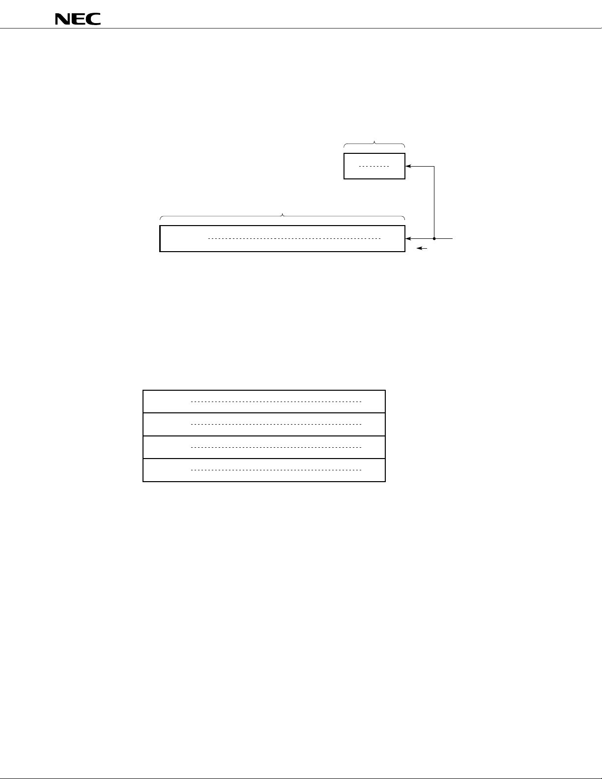
CONFIGURATION OF SHIFT REGISTER
Two shift registers, an 8-bit command register and a 56-bit display register, are provided. The first 8 bits
of input data are recognized as a command and are sent to the command register, and the 9th bit and those
that follow are recognized as display data and are sent to the display register.
8-bit shift register
MSB LSB
56-bit shift register
MSB LSB
SEG56/LED
8
Display data (LCD, LED)
The meaning of the display data is as follows:
LCD: 0 → off, 1 → on
LED: 0 → on, 1 → off
Be sure to transfer 56 bits of display data.
CONFIGURATION OF OUTPUT LATCH
MSB LSB
SEG56/LED
SEG56/LED
SEG56/LED
8
8
8
b7
b0
Command
SEG
1
SEG
1
COM1 (latch address
SEG1COM2 (latch address
SEG1COM3 (latch address
Transfer direction
Note
: 00)
Note
: 01)
Note
: 10)
SEG56/LED
8
Note Bits b3 and b4 of status command (Refer to page 8.)
SEG1COM4 (latch address
Note
: 11)
5
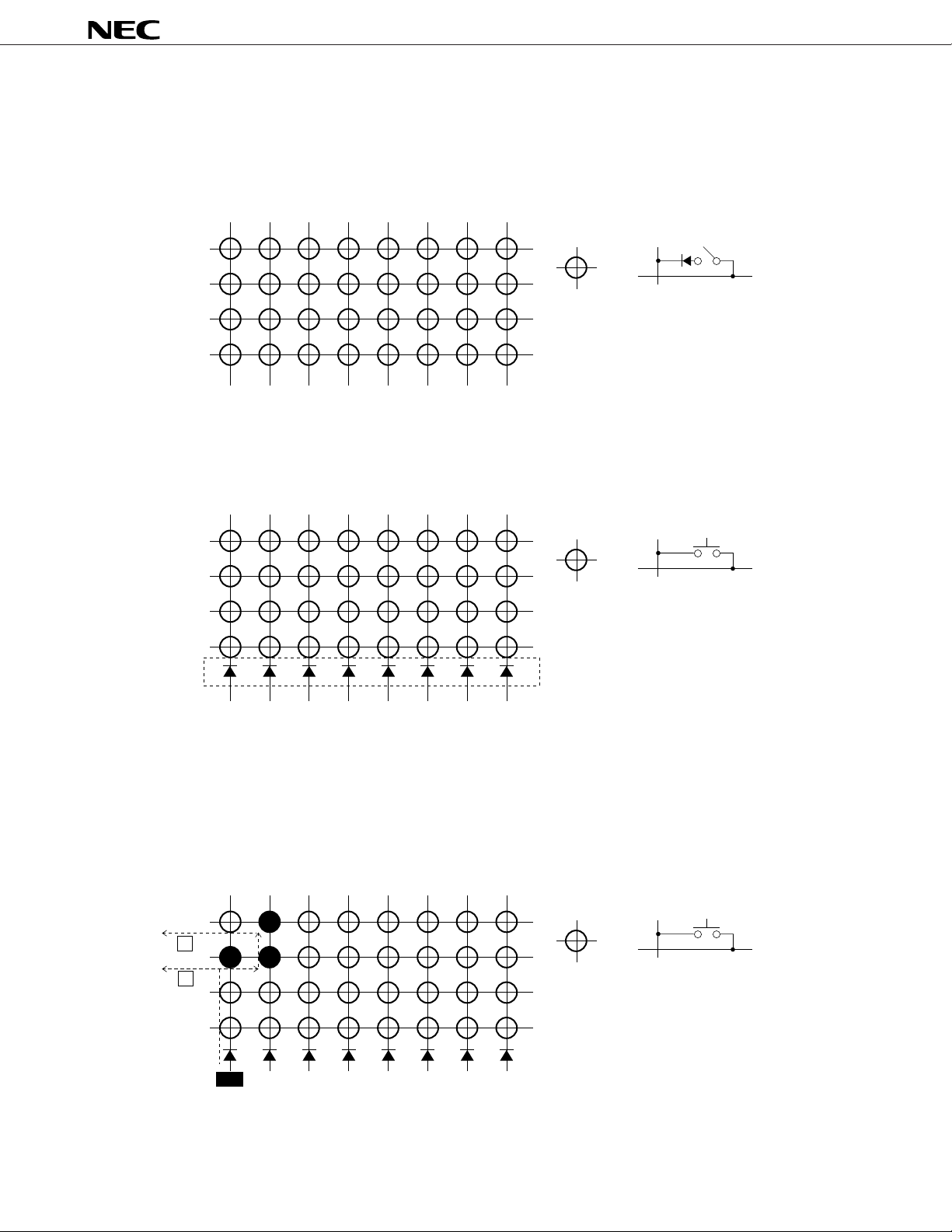
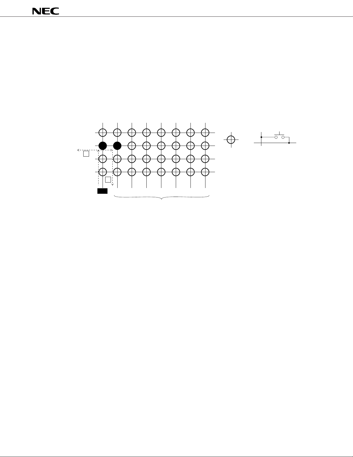
KEY MATRIX CONFIGURATION
An example of key matrix configurations is shown below.
1) When pressing three or more times is assumed:
A configuration example is shown below. In this configuration, 0 to 32 ON switches can be
recognized.
µ
PD16431A
KEY1
=
KEY2
KEY3
KEY4
KS2 KS3 KS4 KS5 KS6 KS7 KS8KS1
C
2) When pressing twice or more times is assumed:
A configuration example is shown below. In this configuration, 0 to 2 ON switches can be recognized.
KEY1
=
KEY2
KEY3
KEY4
Diode A
KS2 KS3 KS4 KS5 KS6 KS7 KS8KS1
In this configuration, pressing three or more times may cause OFF switches to be determined to be ON.
For example, if SW2 to SW4 are ON and KS
1 has been selected (high level) as shown below, SW3 in which
current I1 is running is supposed to be detected to be ON. However, since SW2 and SW4 are ON, current
2 runs thus resulting in SW1 to be recognized as being ON.
I
SW1 SW2
KEY1
=
KEY2
KEY3
KEY4
I2
I1
SW3 SW4
KS2 KS3 KS4 KS5 KS6 KS7 KS8
KS1
Select
6
µ
PD16431A
If diode A is not available, not only the key data may not be read normally but the LCD display may be
affected or ICs may be damaged or deteriorated.
For example, if SW1 and SW2 are ON and KS1 has been selected (high level) as shown below, this will
cause not only current I
1 which is supposed to run but also short-circuited current I2 of KS1 to KS2 to run.
It is possible that this will then cause the following three problems:
(1)Since the level to KEY2 is not correctly sent, the key data cannot be latched correctly.
(2)If KS
2 is used as SEG2 as well, the LCD display may be distorted (such as causing unintended segments
to light up).
(3)Since the short-circuited current (current I2) of KS2 (high level) to KS2 (low level) runs, ICS may be
damaged or deteriorated
KEY1
SW1 SW2
KEY2
I1
KEY3
KEY4
I2
=
KS2 KS3 KS4 KS5 KS6 KS7 KS8
KS1
Select
(high level)
Non Select
(low level)
7
µ
PD16431A
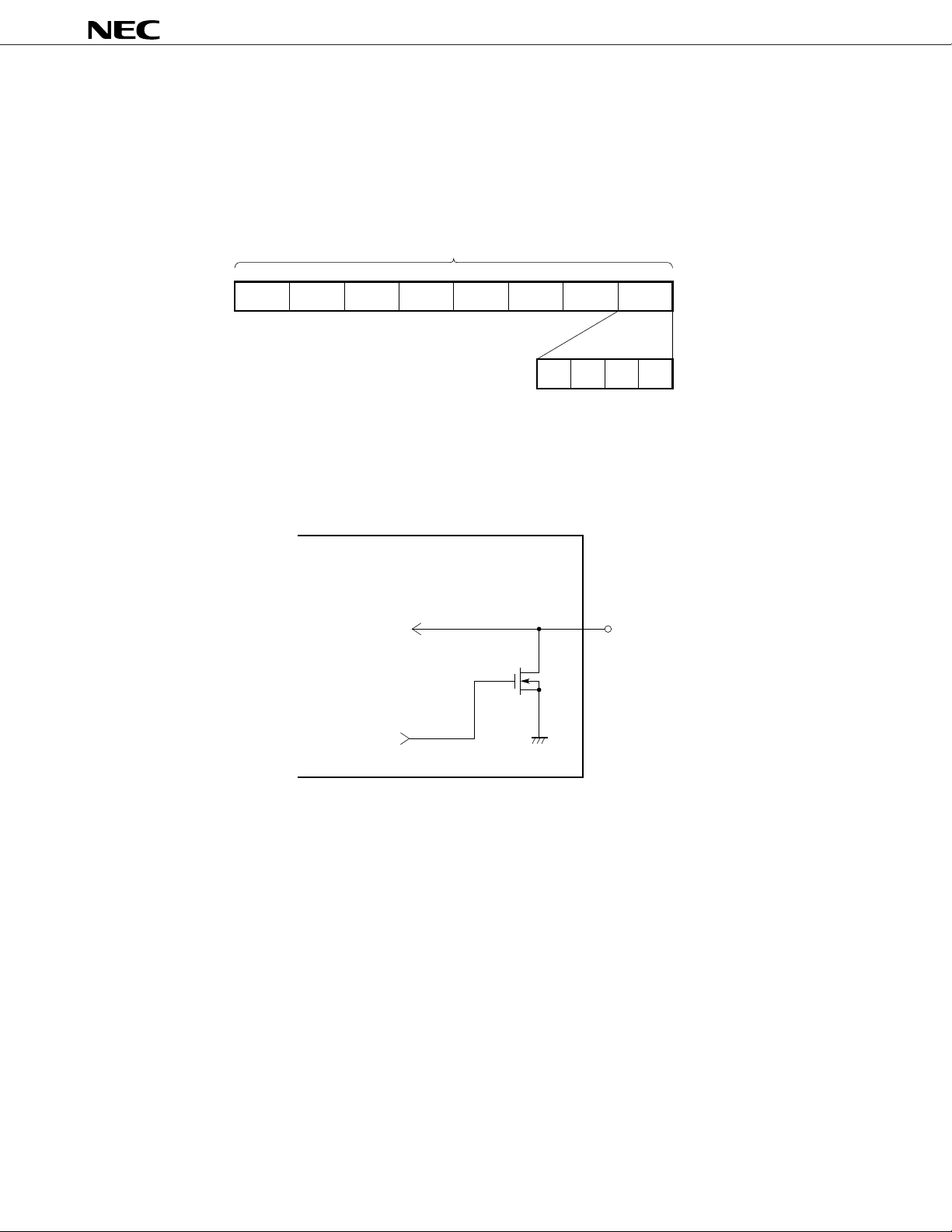
CONFIGURATION OF KEY DATA LATCH
The key data is latched as illustrated below and is read by a read command, starting from the most
significant bit. Key data is read once a frame and latched when coinciding with the immediadtely preceding
data. In other words, it requires at least 2 frames from the time the key is pressed till data is confirmed to
be the key data (the key request becoming H).
32-bit latch/SHIFT register
MSB LSB
KS
KS
8
7
The key data is 0 when off and 1 when on.
KEY INPUT EQUIVALENT CIRCUIT
Pull-down
control signal
KS
3
KEY
4
KS
KEY
KS
6
KS
5
KS
4
KS
KEY
2
1
KEY
1
2
3
KEY nTo key latch
• The pull-down control signal goes high only during key
source output and turns on the pull-down transistor.
• The on-resistance of the pull-down transistor is several kΩ.
8

µ
PD16431A
COMMAND
A command sets a display mode and a status.
The first 1 byte input after the STB pin has fallen is regarded as a command.
If the STB pin is made low while a command/data is transferred, serial communication is initialized, and
the command/data being transferred is made invalid (the command/data that has been already transferred
remains valid, however).
(1) Display setting command
µ
This command initializes the
PD16431A and sets a duty cycle, frame frequency, drive voltage supply
method, test mode, and whether the µPD16431A operates as the master or a slave.
When this command is executed, display is forcibly turned off and key scanning is stopped. To resume
the display, the normal operation of the “status command” must be executed. Note, however, that nothing
is executed if the same mode is selected.
MSB LSB
b0
b1b2b3b4b5b60
Sets duty.
00: 1/4 duty, 1/3 bias
01: 1/3 duty, 1/3 bias
10: 1/2 duty, 1/2 bias
11: 1/2 duty, 1/2 bias
Sets frame frequency.
OSC
/128) × n
00: (f
01: (f
OSC
/256) × n
OSC
/512) × n
10: (f
11: (f
OSC
/1024) × n
n= duty (1/2, 1/3, 1/4)
Sets drive voltage supply method.
0: Internal
1: External
Sets master or slave.
0: Master
1: Slave
Sets test mode.
0: Normal operation
1: Test mode
Values when power is applied
0
000000
9

(2) Status command
This command sets a data write/read mode, turns on/off display, and sets a latch address.
MSB LSB
µ
PD16431A
Values when power is applied
b0
b1b2b3b4××1
0
0000××
× : Don’t Care
Sets data write/read mode.
0: Writes display data to output latch
1: Reads key data
Turns on/off display
00: Forcibly turns off display (all segments and LEDs off).
Stops key scanning.
01: Prohibited
10: Normal operation
11: Don’t care
Sets latch address.
00: COM
01: COM
10: COM
11: COM
1
2
3
4
10

OUTPUT SELECT VOLTAGE
1. COM
+ – Bias
When selected VLCD GND 1/2 bias
VLCD GND
When not selected 1/2 VLCD 1/2 VLCD
VLC2 VLC2
When key scanned 1/2 VLCD 1/2 VLCD
VLC2 VLC2
When selected VLCD GND 1/3 bias
VLCD GND
When not selected 1/3 VLCD 2/3 VLCD
VLC3 VLC1
When key scanned 1/2 VLCD 1/2 VLCD
VLC2 VLC2
µ
PD16431A
Top : with internal power supply
Bottom: with external power supply
2. SEG
+ – Bias
When selected GND VLCD 1/2 bias
GND VLCD
When not selected VLCD GND
VLCD GND
When key scanned GND VLCD
GND VLCD
When key not VLCD GND
scanned VLCD GND
When selected GND VLCD 1/3 bias
GND VLCD
When not selected 2/3 VLCD 1/3 VLCD
VLC1 VLC3
When key scanned GND VLCD
GND VLCD
When key not VLCD GND
scanned VLCD GND
11
 Loading...