NEC UPD16334 Datasheet

DATA SHEET
MOS INTEGRATED CIRCUIT
µµ
µ
PD16334
µµ
96-Bit AC-PDP DRIVER
The µPD16334 is a high-voltage CMOS driver designed for flat display panels such as PDPs, VFDs and ELs. It
consists of a 96-bit bi-directional shift register, 96-bit latch and high-voltage CMOS driver. The logic block is designed
to operate using a 5-V power supply/3.3-V interface enabling direct connection to a gate array or a microcontroller.
µ
In addition, the
withstand voltage output (80 V, 50 mA).
FEATURES
•Selectable by IBS pin; three 32-bit bi-directional shift register circuits
configuration or six 16-bit bi-directional shift register circuits configuration
•Data control with transfer clock (external) and latch
•High-speed data transfer(f
•High withstand output voltage (80 V, 50 mA
•3.3 V CMOS input interface
•High withstand voltage CMOS structure
•Capable of reversing all driver outputs by PC pin
PD16334 achieves low power dissipation by employing the CMOS structure while having a high
max. = 25 MHz min. at data fetch)
(fmax. = 15 MHz min. at cascade connection)
MAX.)
ORDERING INFORMATION
Part Number Package
µ
PD16334 COB*
* Please consult with an NEC sales representative about COB.
DocumentNo. S12362EJ2V0DS00 (2nd edition)
Date Published May 1998 N CP(K)
Printed in Japan
©
1997

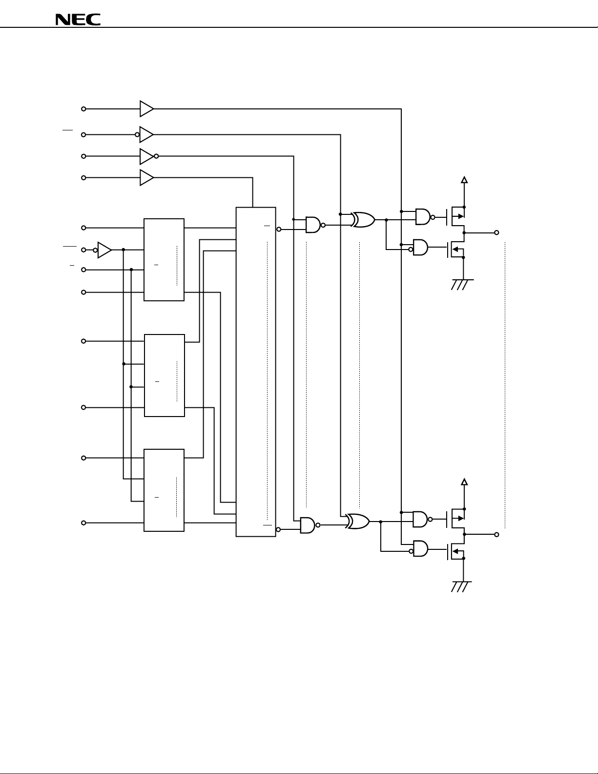
BLOCK DIAGRAM (IBS = H, 3-BIT INPUT, 32-BIT LENGTH SHIFT REGISTER)
OE
PC
BLK
LE
SR1
S
1
A
CLK
A
CLK
1
1
S
4
S
1
L
1
S
2
S
3
µµ
µ
µµ
V
DD2
PD16334
O
1
R/L
B
A
B
A
B
1
2
2
3
3
SRn: 32-bit shift register
R/L
1
B
A
2
CLK
R/L
B
2
A
3
CLK
R/L
3
B
SR2
SR3
V
SS2
S
94
S
2
S
5
S
95
S
3
S
6
94
S
S
95
S
S
96
96
L
96
V
DD2
O
96
V
SS2
2

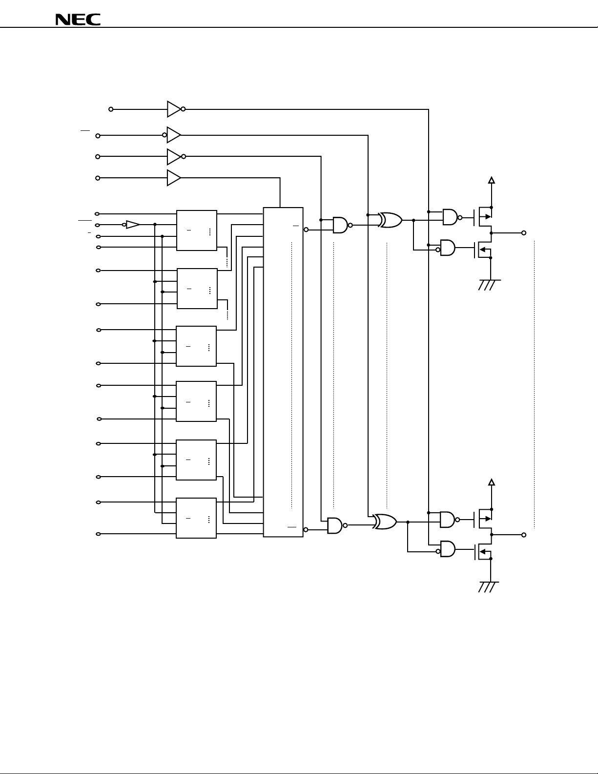
BLOCK DIAGRAM (IBS = L, 6-BIT INPUT, 16-BIT LENGTH SHIFT REGISTER)
OE
PC
BLK
LE
µµ
µ
PD16334
µµ
V
DD2
A
CLK
R/L
B
A
B
A
B
A
B
A
B
A
B
1
1
2
2
A
1
CLK
R/L
1
B
A
2
CLK
R/L
B
2
SR1
SR2
S
1
S
7
S
91
S
2
S
8
S
92
S1 LE
S
2
S
3
S
4
S
5
S
6
L
1
O
1
V
SS2
SR3
3
3
A
3
CLK
R/L
B
3
S
3
S
9
S
93
SR4
4
4
A
4
CLK
R/L
4
B
S
4
S
10
S
94
SR5
5
5
6
6
A
5
CLK
R/L
B
5
A
6
CLK
R/L
B
6
SR6
S
5
S
11
S
95
S
S
6
S
12
S
96
93
S
94
S
95
L
96
S
96
V
DD2
O
96
SRn: 16-bit shift register
V
SS2
3

µµ
µ
PD16334
µµ
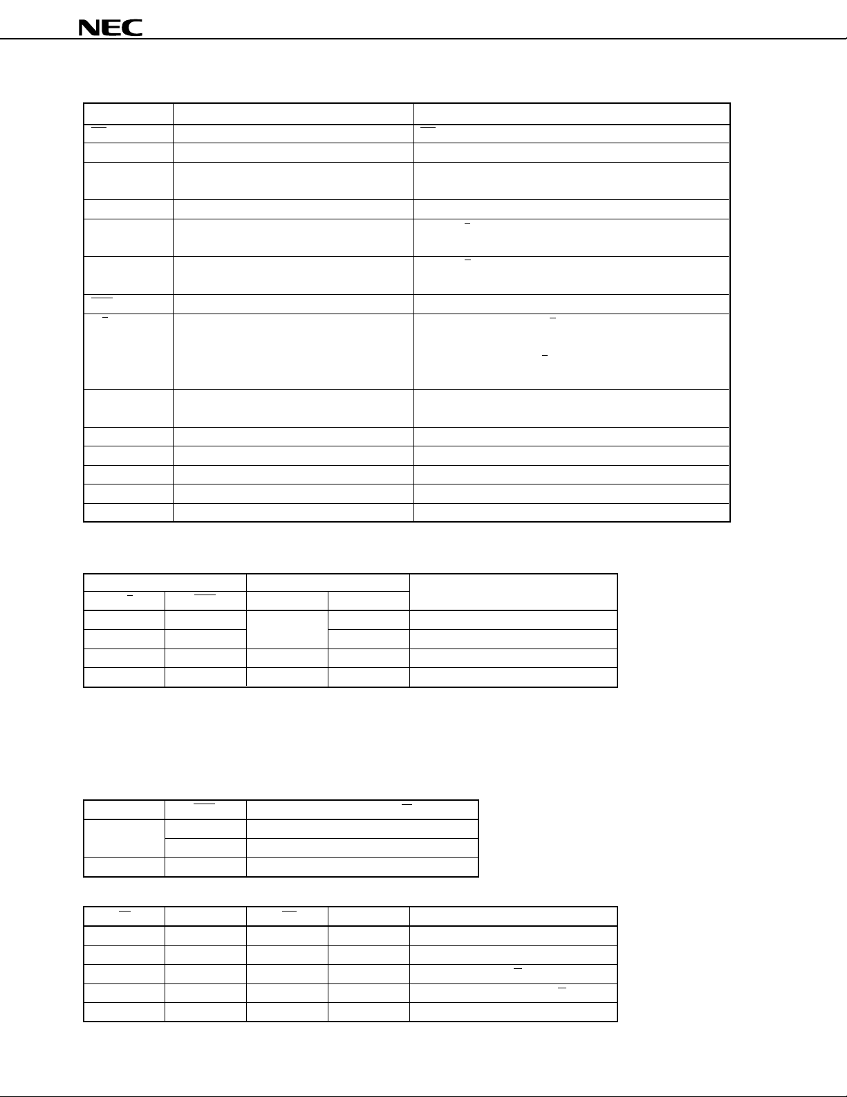
PIN DESCRIPTION
Symbol Pin Name Description
PC Polarity change input PC = L: All driver output invert
BLK Blank input BLK = H : All output = H or L
LE Latch enable input Automatically executes latch by setting high at rising edge
of the clock
OE Output enable Make output high impedance by input H
(Note)
(Note)
When R/L=H (values in parentheses are for 6-bit input)
A1 to A3 (6) : Input B1 to B3 (6) : Output
When R/L=L (values in parentheses are for 6-bit input)
A1 to A3 (6) : Output B1 to B3 (6) : Input
SR1 : A1 → S1...S94 → B1 (Same direction for SR2 to SR6)
Left shift mode when R/L= L
SR1 : B1 → S94...S1 → A1 (Same direction for SR2 to SR6)
L: 16-bit length shift register, 6-bit input
A1 to A3 (6) RIGHT data input/output
B1 to B3 (6) LEFT data input/output
CLK Clock input Shift executed on fall
R/L Shift control input Right shift mode when R/L= H
IBS Input mode switch H: 32-bit length shift register, 3-bit input
O1 to O96 High withstand voltage output 80 V, 50 mAMAX.
VDD1 Power supply for logic block 5 V ± 10 %
VDD2 Power supply for driver block 10 to 70 V
VSS1 Logic GND Connect to system GND
VSS2 Driver GND Connect to system GND
Note When input mode is 3-bit, set unused input and output pins “L” level.
TRUTH TABLE 1 (Shift Register Block)
Input Output
R/L CLK A B
H ↓ Input Output
H H or L Output Hold
L ↓ Output
L H or L Output Hold
Note2
Note1
Input Left shift execution
Right shift execution
Notes1. The data of S91 to S93 (S85 to S90) shifts to S94 to S96 (S91 to S96) and is output from B1 to B3 (B1 to B6) at the falling
edge of the clock, respectively. (Values in parentheses are for 6-bit input)
2. The data of S
4 to S6 (S7 to S12) shifts to S1 to S3 (S1 to S6) and is output from A1 to A3 (A1 to A6) at the falling
edge of the clock, respectively (Values in parentheses are for 6-bit input)
Shift Register
TRUTH TABLE 2 (Latch Block)
LE CLK Output State of Latch Block (Ln)
H ↑ Latch Sn data and hold output data
↓ Hold latch data
L X Hold latch data
TRUTH TABLE 3 (Driver Block)
Ln BLK PC OE Output State of Driver Block
X H H L H (All driver outputs: H)
X H L L L (All driver outputs: L)
X L H L Output latch data (Ln)
X L L L Output inverted latch data (Ln)
X X X H Set output impedance high
X: H or L, H: High level, L: Low level
4
 Loading...