

NEC UPD16312GB-3B4 Datasheet
DATA SHEET
MOS INTEGRATED CIRCUIT
PD16312
1/4- to 1/11-DUTY FIPTM (VFD) CONTROLLER/DRIVER
The
PD16312 is a FIP (fluorescent Indicator Panel, or Vacuum Fluorescent Display) controller/driver that is
driven on a 1/4- to 1/11 duty factor. It consists of 11 segment output lines, 6 grid output lines, 5 segment/grid output
drive lines, a display memory, a control circuit, and a key scan circuit. Serial data is input to the PD16312 through a
three-line serial interface. This FIP controller/driver is ideal as a peripheral device for a single-chip microcomputer.
FEATURES
•Multiple display modes (11-segment & 11-digit to 16-segment & 4-digit)
•Key scanning (6 4 matrix)
•Dimming circuit (eight steps)
•High-voltage output (VDD 35 V max).
•LED ports (4 chs., 20 mA max).
•General-purpose input port (4 bits)
•No external resistors necessary for driver outputs (P-ch open-drain + pull-down resistor output)
•Serial interface (CLK, STB, DIN, D
OUT
)
ORDERING INFORMATION
Part Number Package
PD16312GB-3B4 44-pin plastic QFP ( 10)
Document No. IC-3307 (1st edition)
Date Published March 1997 P
Printed in Japan
1993©
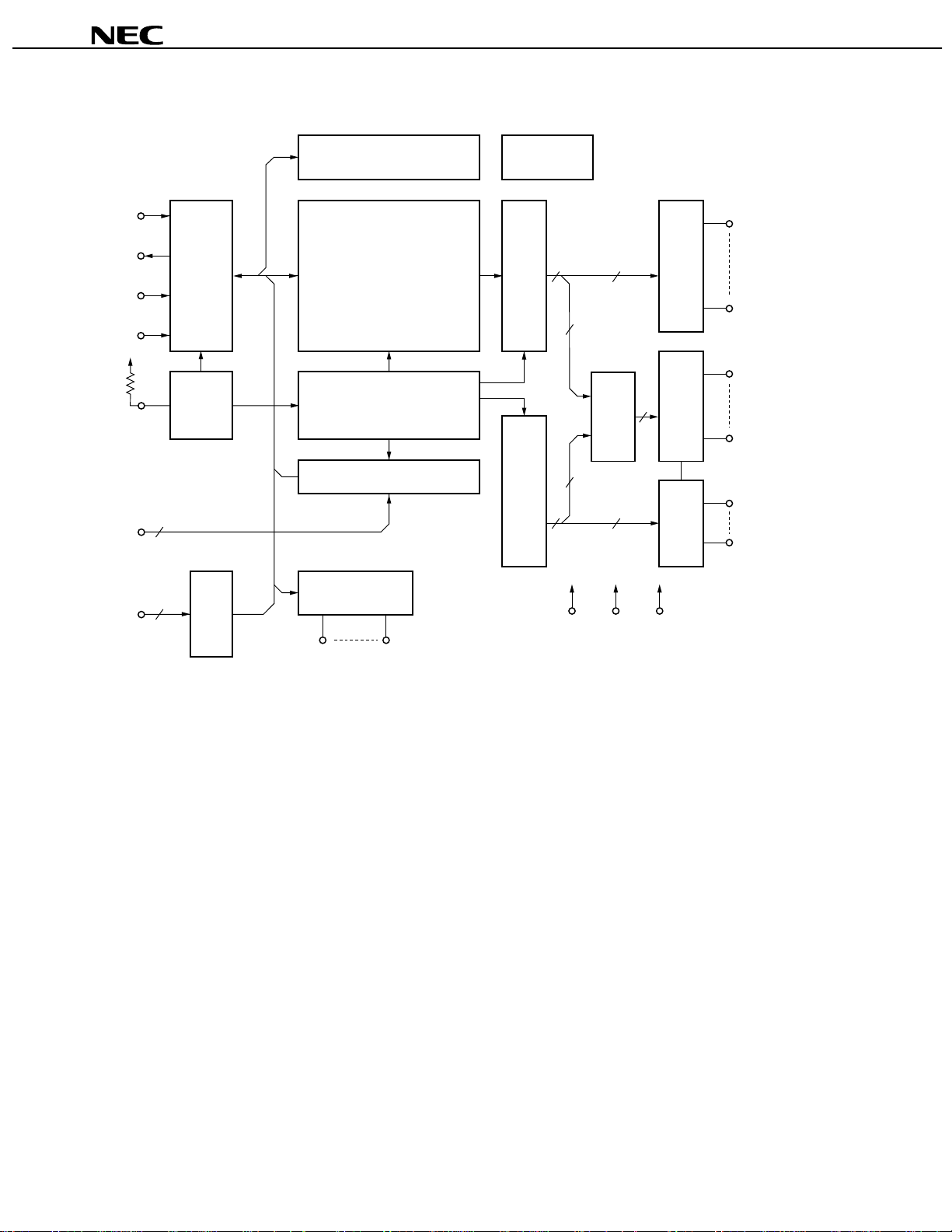
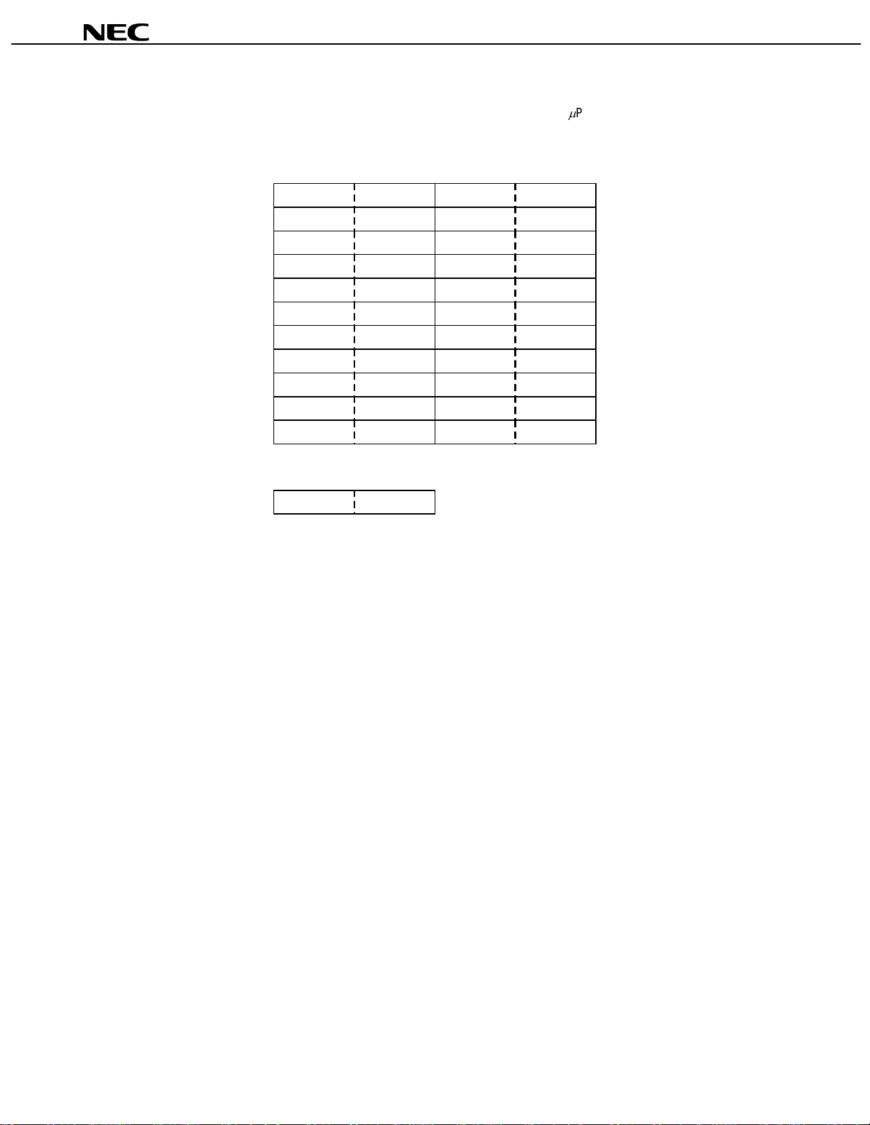
BLOCK DIAGRAM
PD16312
D
CLK
STB
V
DD
Key
to
Key
SW
to
SW
D
OUT
Command decoder
IN
Serial I/F
Display memeory
16 bits × 11 words
Dimming circuit
16-bit
16 11
output
latch
Segment
driver
Seg
Seg
1
11
5
R
OSC
Timing generator key scan
Key data memory (4 × 6)
11-bit
shift
Data
selector
5
5
Multip lexed
register
V
EE
(−30 V)
Grid
driver
1
4
4
1
4
4-bit
latch
4
4-bit latch
LED
1
LED
4
11 6
V
V
DD
(+5 V)
(0 V)
SS
Seg12/Grid
diver
Seg16/Grid
Grid
Grid
11
7
1
6
Key data memory (4 × 6)
2
PIN CONFIGURATION (Top View)
SS43
OSC44
V
142
LED
241
LED
340
LED
439
LED
DD38
V
137
Grid
236
Grid
335
Grid
434
Grid
PD16312
SW1 1
2 2
SW
3 3
SW
4 4
SW
OUT 5
D
IN 6
D
SS 7
V
CLK 8
STB 9
1 10
KEY
2 11
KEY
KEY3 12
4 13
KEY
DD 14
V
1/KS1 15
Seg
2/KS2 16
Seg
3/KS3 17
Seg
4/KS4 18
Seg
5/KS5 19
Seg
6/KS6 20
Seg
7 21
Seg
8 22
Seg
Grid533
Grid
Seg
Seg
Seg
Seg
EE27
V
Seg
Seg
Seg
Seg
632
16/Grid731
15/Grid830
14/Grid929
13/Grid1028
12/Grid1126
1125
1024
923
Use all power pins.
3
PD16312
Pin Function
Symbol Pin Name Pin No Description
IN
D
OUT
D
STB Strobe 9 Initializes serial interface at the rising or falling edge of the
CLK Clock input 8 Reads serial data at the rising edge, and outputs data at the
OSC Oscillator pin 44 Connect resistor to this pin to determine the oscillation frequency
Seg1/KS1 to
6
6
/KS
Seg
Seg7 to Seg
Grid1 to Grid
11
6
Seg12/Grid11 to
16
7
/Grid
Seg
LED1 to LED
KEY1 to KEY
SW1 to SW
DD
V
SS
V
EE
V
4
4
4
Data input 6 Input serial data at rising edge of shift clock, starting from the low
order bit.
Data output 5 Output serial data at the falling edge of the shift clock, starting
from low order bit. This is N-ch open-drain output pin.
PD16312. It then waits for reception of a command. Data input
after STB has fallen is processed as a command. While
command data is processed, current processing is stopped, and
the serial interface is initialized. While STB is high, CLK is
ignored.
falling edge.
to this pin.
High-voltage output 15 to 20 Segment output pins (Dual function as key source)
High-voltage output
21 to 25 Segment output pins
(segment)
High-voltage output (grid) 37 to 32 Grid output pins
High-voltage output
26, 28 to 31
These pins are selectable for segment or grid driving.
(segment/grid)
LED output 42 to 39 CMOS output. +20 mA max.
Key data input 10 to 13 Data input to these pins is latched at the end of the display cycle.
Switch input 1 to 4 These pins constitute a 4-bit general-purpose input port.
Logic power 14, 38 5 V 10 %
Logic ground 7, 43 Connect this pin to system GND.
Pull-down level 27 VDD 35 V max.
4
PD16312
Display RAM Address and Display Mode
The display RAM stores the data transmitted from an external device to the PD16312 through the serial interface,
and is assigned addresses as follows, in 8 bits unit:
Seg
0
b
1
00H
02H
04H
06H
08H
0AH
0CH
0EH
10H
12H
14H
xxH
L
L
L
L
L
L
L
L
L
L
L
L
Seg
b3b
4
00H
02H
04H
06H
08H
0AH
0CH
0EH
10H
12H
14H
4
xxH
Lower 4 bits Higher 4 bits
8
Seg
U
U
U
U
U
U
U
U
U
U
U
U
01H
03H
05H
07H
09H
0BH
0DH
0FH
11H
13H
15H
7
b
Seg
L
L
L
L
L
L
L
L
L
L
L
12
01H
03H
05H
07H
09H
0BH
0DH
0FH
11H
13H
15H
U
U
U
U
U
U
U
U
U
U
U
Seg
16
1
DIG
2
DIG
3
DIG
4
DIG
5
DIG
6
DIG
7
DIG
8
DIG
9
DIG
10
DIG
11
DIG
5
PD16312
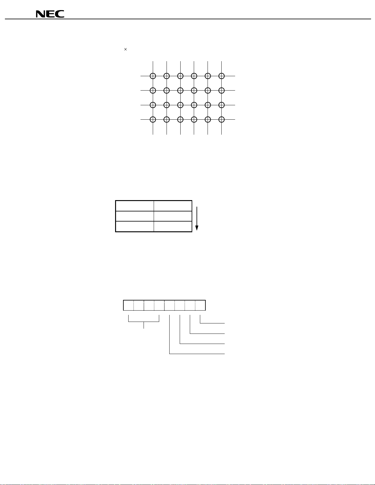
Key Matrix and Key-Input Data Storage RAM
The key matrix is made up of a 6 4 matrix, as shown below.
KEY
1
KEY
2
KEY
3
KEY
4
1
2
3
4
5
6
/KS
/KS
/KS
/KS
/KS
1
Seg
2
Seg
3
Seg
4
Seg
5
Seg
/KS
6
Seg
The data of each key is stored as illustrated below, and is read with the read command, starting from the least
significant bit.
KEY1…KEY4KEY1…KEY
4
Seg1/KS
Seg3/KS
Seg5/KS
1
3
5
Seg2/KS
Seg4/KS
Seg6/KS
2
4
6
Reading sequence
b0------------b3 b4------------b7
LED Port
Data is written to the LED port with the write command, starting from the least port’s least significant bit. When a
bit of this port is 0, the corresponding LED lights; when the bit is 1, the LED truns off. The data of bits 5 through 8 are
ignored.
MSB
−−−−b3 b2 b1 b0
Don't care
LSB
LED1
LED2
LED3
LED4
On power application, all LEDs are unlit.
6
 Loading...