NEC UPC8172TB-E3, UPC8172TB Datasheet

PRELIMINARY DATA SHEET
BIPOLAR ANALOG INTEGRATED CI RCUIT
PC8172TB
µµµµ
SILICON MMIC 2.5 GHz FREQUENCY UP-CONVERTER
FOR WIRELESS TRANSCEIVER
DESCRIPTION
The µPC8172TB is a silicon monolithic integrated circuit designed as frequency up-converter for wireless
transceiver transmitter stage. This IC is manufactured using NEC’s 30 GHz f
silicon bipolar process.
This IC is as same circuit current as conventional µPC8106TB, but operates at higher frequency, higher gain and
lower distortion. Consequently this IC is suitable for mobile communications.
FEATURES
• Recommended operating frequency : f
• Higher IP
• High-density surface mounting : 6-pin super minimold package
• Supply voltage : VCC = 2.7 to 3.3 V
3
RFout
= 0.8 to 2.5 GHz
: CG = 9.5 dB TYP., OIP3 = +7.5 dBm TYP. @ f
max.
UHS0 (Ultra High Speed Process)
RFout
= 0.9 GHz
APPLICATIONS
• PCS1900M
• 2.4 GHz band transmitter/receiver system (wireless LAN etc.)
ORDERING INFORMATION
Part Number Package Marking Supplying Form
µ
PC8172TB-E3 6-pin super minimold C3A
Remark
To order evaluation samples, please contact your local NEC sales office.
(Part number for sample order:
PC8172TB)
µ
•
Embossed tape 8 mm wide.
•
Pin 1, 2, 3 face the tape perf oration side.
•
Qty 3 kpcs/reel.
The information in this document is subject to change without notice. Before using this document, please
confirm that this is the latest version.
Not all devices/types available in every country. Please check with local NEC representative for
availability and additional information.
Document No. P14729EJ1V0DS00 (1st edition)
Date Published June 2000 N CP(K)
Printed in Japan
Caution Electro-static sensitive devices
©
2000

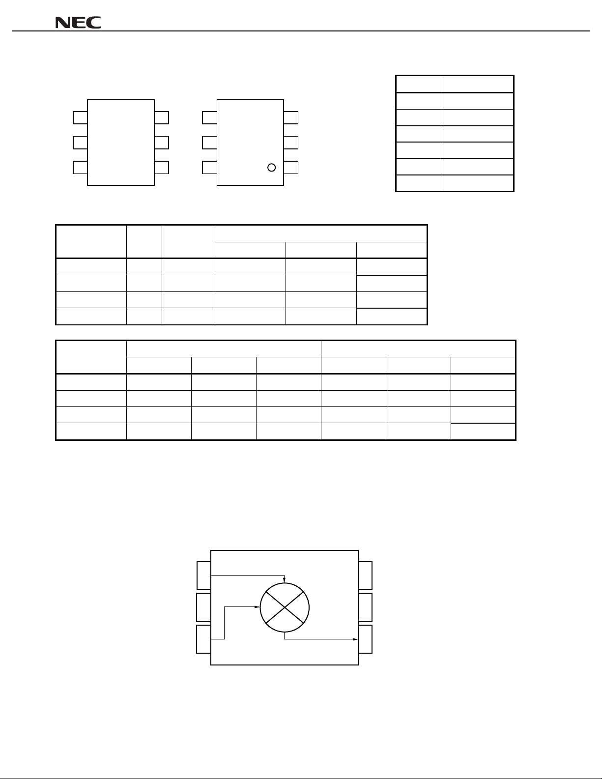
PIN CONNECTIONS
µµµµ
PC8172TB
(Top View)
3
2
1
C3A
SERIES PRODUCTS (T
CC
Part Number
PC8172TB 9 0.8 to 2.5 9.5 8.5 8.0
µ
PC8106TB 9 0.4 to 2.0 9 7
µ
PC8109TB 5 0.4 to.2.0 6 4
µ
PC8163TB 16.5 0.8 to 2.0 9 5.5
µ
Part Number
I
(mA)
@RF 0.9 GHz
4
4
5
5
6
6
= +25°C, VCC = VPS = V
A
RFout
f
(GHz)
Note
(Bottom View)
3
2
1
= 3.0 V, ZS = ZL = 50
RFout
CG (dB)
@RF 0.9 GHz
O(sat)
P
(dBm) OIP3 (dBm)
@RF 1.9 GHz @RF 2.4 GHz
Note
@RF 1.9 GHz @RF 2.4 GHz
@RF 0.9 GHz
Pin No. Pin Name
1 IFinput
2GND
3 LOinput
4PS
5V
6 RFoutput
)
ΩΩΩΩ
−
−
−
Note
@RF 1.9 GHz @RF 2.4 GHz
CC
PC8172TB +0.5 0
µ
PC8106TB
µ
PC8109TB
µ
PC8163TB +0.5
µ
RFout
= 0.83 GHz @ µPC8163TB
f
Note
Remark
Typical performance. Please refer to
2
−
5.5
−
To know the associated product, please refer to each latest data sheet.
BLOCK DIAGRAM (FOR THE
LOinput
GND
IFinput
4
−
7.5
−
2
−
PC8172TB)
µµµµ
0.5 +7.5 +6.0 +4.0
−
−
−
−
+5.5 +2.0
+1.5
+9.5 +6.0
ELECTRICAL CHARACTERISTICS
(Top View)
PS
V
RFoutput
in detail.
CC
−
1.0
−
−
−
2
Preliminary Data Sheet P14729EJ1V0DS00

µµµµ
PC8172TB
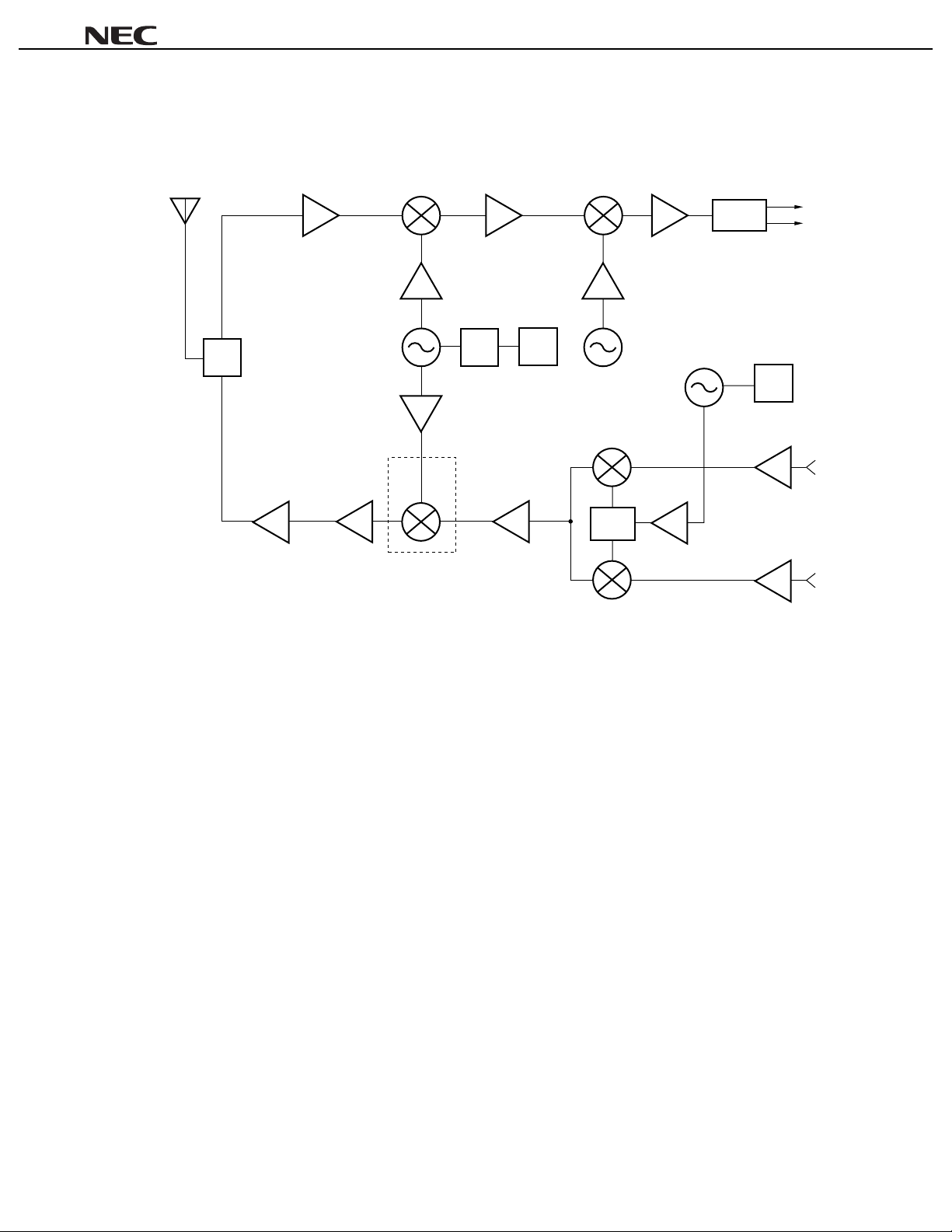
SYSTEM APPLICATION EXAMPLES (SCHEMATICS OF IC LOCATION IN THE SYSTEM)
Wireless Transceiver
Low Noise Tr.
RX
DEMOD.
I
Q
PLL
TX
SW
PA
VCO
PC8172TB
µ
÷N
To know the associated products, please refer to each latest data sheet.
PLL
I
0°
Phase
shifter
90°
Q
Preliminary Data Sheet P14729EJ1V0DS00
3

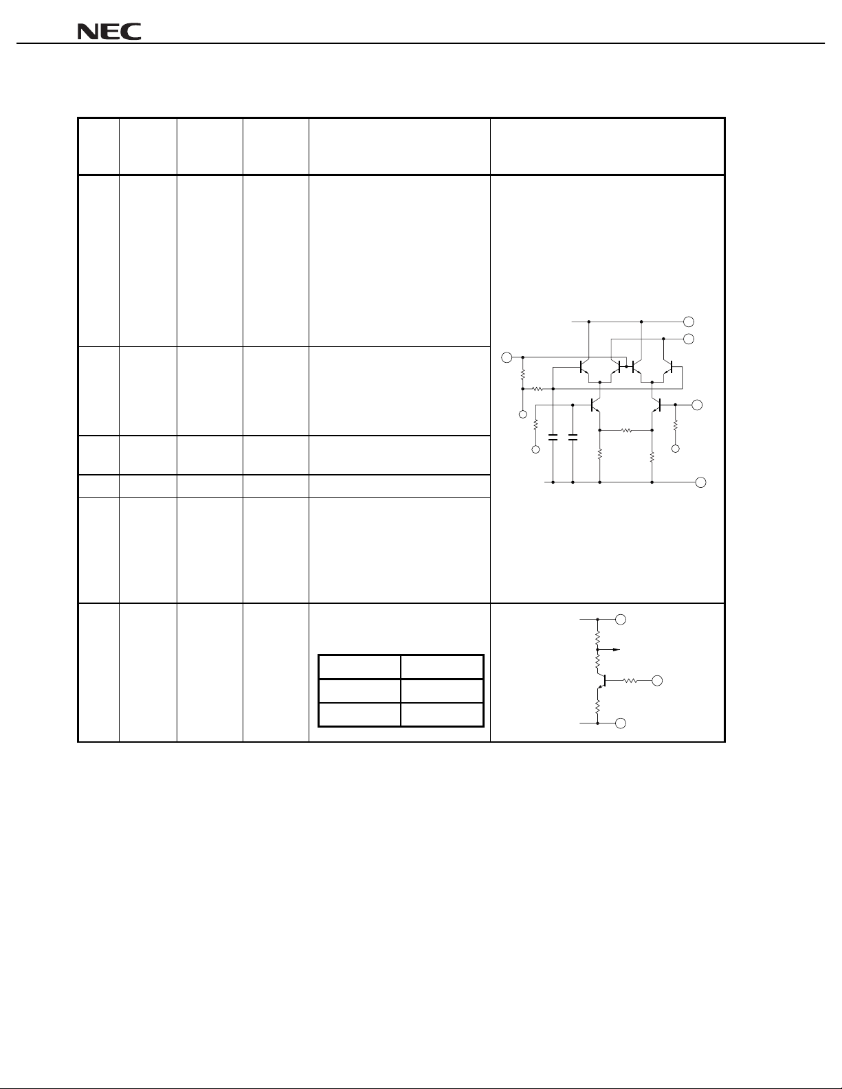
PIN EXPLANATION
µµµµ
PC8172TB
Pin
No.
1 IFinput
2GND GND
3 LOinput
5VCC2.7 to 3.3
6 RFoutput Same
4PS VCC/GND
Pin
Name
Applied
Voltage
(V)
−
−
bias as
CC
V
through
external
inductor
Pin
Voltage
Note
(V)
1.4 This pin is IF input t o doubl e bal -
−
2.3 Local input pin. Recommendable
−
−
−
Function and Explanation Equivalent Circuit
anced mixer (DBM). The input i s
designed as high impedance.
The circuit contributes to suppress spurious signal. A l so this
symmetrical ci rcuit can keep
specified performance insensitive
to process-condition distribution.
For above reason, double balanced mixer is adopted.
GND pin. Ground pattern on the
board should be formed as wide
as possible. Track Lengt h should
be kept as short as poss i bl e to
minimize ground impedance.
input level is −10 to 0 dBm.
Supply voltage pin.
This pin is RF output from DB M .
This pin is designed as open
collector. Due to the high i m pedance output, this pin s houl d be
externally equipped with LC
matching circuit t o next stage.
Power save control pin. B i as
controls operation as foll ows.
5
6
3
1
2
V
CC
5
Each pin voltage is measured with V
Note
4
Pin bias Control
CC
V
GND Power Save
CC
= VPS = V
Preliminary Data Sheet P14729EJ1V0DS00
RFout
Operation
= 3.0 V.
GND
4
2
 Loading...