NEC UPC8139GR-7JH-E1, UPC8139GR-7JH Datasheet

PRELIMINARY DATA SHEET
BIPOLAR ANALOG INTEGRATED CI RCUIT
µµµµ
PC8139GR-7JH
Single Chip Transceiver Silicon MMIC for PHS
DESCRIPTION
The µPC8139GR-7JH is a silicon microwave monolithic IC (SiMMIC) developed as a transceiver for Personal
Handyphone System (PHS).
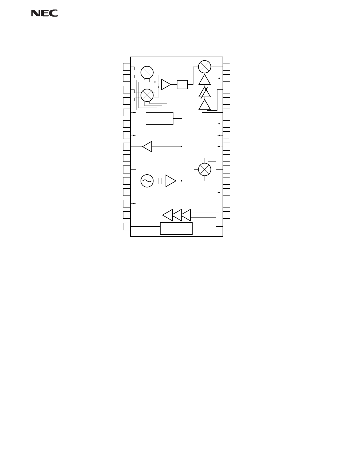
This IC is a highly integrated single chip, suitable for PHS, including a quadrature modulator, up converter, and
AGC circuit for adjusting the output level in the transmitter block, a 2nd down converter and RSSI circuit in the
receiver block, and a transistor for 2nd VCO.
This low power IC employs NEC’s proprietary bipolar process NESATTM IV (fT = 20 GHz) and also has a built-in
power save function, which contributes to lowering power consumption of the RF block.
This IC is packaged in a small, thin 30 pin plastic TSSOP (225 mil).
FEATURES
• Low voltage operation, low current consumption
VCC = 2.7 to 4.0 V, ICC = 32.5 mA at transmitter, ICC = 4.8 mA at receiver, 3.2 mA/@VCC = 3 V at 2nd VCO block
• LPF is installed to suppress leakage of transmitter’s local (L01) harmonics.
Spurious within transmission band (LO1 × 7, 8): –55 dBc (MAX.)
• On-chip AGC circuit for adjusting the output level: GCR = 20 dB (MIN.) /@f
• High-performance
Output level: P
Error vector magnitude: EVM = 1.0% rms (TYP.)
Adjacent channel leak power: P
RSSI output dynamic range: 83 dB
• CR phase shifter is adopted.
RFout
= –13 dBm (TYP.) /@f
adj
= –68 dBc (TYP.) /@∆f = ±600 kHz
RFout
= 1906.55 MHz, V
RFout
I/Q
= 500 mV
= 1906.55 MHz
P-P
(Differential phase)
APPLICATION
• Digital cordless telephone: PHS
• PHS application equipment: PDA, PC card, etc.
ORDERING INFORMATION
Part Number Package Supplying Form
µ
PC8139GR-7JH-E1 30-pin plastic TSSOP (225 m i l) Embossed tape 16 mm-wide. P i n 1 is in pull-out direction. 2.5
kp/reel
Remark
Caution This product is an electrostatic sensitive device.
Document No. P13117EJ1V0DS00 (1st edition)
Date Published December 1998 N CP(K)
Printed in Japan
To order evaluation samples, contact your local NEC sales office. (Part Number for sample order:
PC8139GR-7JH)
µ
The information in this document is subject to change without notice.
©
1998

SYSTEM APPLICATION EXAMPLE
µµµµ
PC8139GR-7JH
[PHS]
243.95 MHz
or
248.45 MHz
PLL1
LPFBPFPA
SAW
PLL2
PC8139GR-7JH
µ
1895.15 to 1917.95 MHz
or
(1906.55±11.4 MHz)
MAIN ANT
PC8112
µ
LNAATT BPF
1651.2 to 1674.0 MHz
or
1646.7 to 1669.5 MHz
1662.0 to 1684.8 MHz
or
1635.9 to 1658.7 MHz
1st MIX
1st LO
SWSW
2SC5006
AGC
QUADRATURE MODULATOR IC SERIES PRODUCT LIST
Part Number Function I
PC8101GR 150-MHz quadrature
µ
modulator
PC8104GR RF up converter + IF
µ
quadrature modulator
PC8105GR 400-MHz quadrature
µ
modulator 16
PC8110GR 1-GHz direc t
µ
quadrature modulator24/@3.0 V
PC8125GR On-chip AGC function
µ
RF up converter + IF
quadrature modulator
PC8126GR
µ
On-chip local PreMIX
1-GHz direct
PC8126K
µ
PC8129GR LO × 2 frequency
µ
quadrature modulator
input type IF
quadrature modulator
+ RF up converter
PC8158K On-chip AGC function
µ
RF up converter + IF
quadrature modulator
CC
(mA)
15
/@2.7 V
28
/@3.0 V
/@3.0 V
36
/@3.0 V
35
/@3.0 V
28
/@3.0V
28
/@3.0 V
LO1in
f
(MHz)
100 to
300
MODout
f
(MHz)UpConverter
50 to
150
100 to 400 900 to 1900
100 to 400 External
800 to 1000
220 to 270
915 to 960
200 to
800
100 to
400
100 to 300 800 to 1500 CR
10.8 MHz
2nd MIX BPF
φ
2nd LO
0˚
(CR)
90˚
233.15 MHz
or
259.25 MHz
Phase
Application
Shifter
RFout
f
(MHz)
Type
External F/F CT-2, etc.
Various
Multiplier
+ F/F
digital
communica-
tions
Various
Multiplier
+ F/F
digital
communica-
tions
Direct
modulation
1800 to
2000
Direct
modulation
Multiplier
+ F/F
Multiplier
+ F/F
Multiplier
+ F/F
PDC800
MHz, etc.
PHS
PDC800
MHz, etc.
GSM,
800 to 1900 F/F
DCS1800,
etc.
PDC800
M/1.5 G
To DEMOD.
RSSI OUTRSSI
I
Q
Package
Field
20 pin
SSOP
(225 mil)
16 pin
SSOP
(225 mil)
20 pin
SSOP
(225 mil)
28 pin
QFN
20 pin
SSOP
(225 mil)
28 pin
QFN
For an outline of the quadrature modulator IC series, see the application note “Usage of µPC8101, 8104, 8105, 8125,
and 8129” (document number P13251E).
2
Preliminary Data Sheet

INTERNAL BLOCK DIAGRAM AND PIN CONNECTIONS (Top View)
µµµµ
PC8139GR-7JH
1I
2Ib
IQ Mix.
3Q
Adder
4Qb
5V
CC
1
6GND1
CC
2
7V
90˚ Phase shifter
(CR)
8VCOout
LO Buff.
9GND2
10VCO-E
11VCO-B
2nd VCO
12VCO-C
CC
3
13V
LO Buff.
14IFout
15RSSIout
Up Con.
LPF
2nd IF Amp
RSSI
AGC
2nd Mix
24
21
TX MIXout30
CC
629
V
TX MIX-LOin28
GND527
TX MIX-LOinb26
V
CC
525
VPS (TX) /V
VPS (RX)23
2nd MIXin22
2nd MIXinb
2nd MIXout20
CC
419
V
GND318
IFin217
IFin116
AGC
Note
Pin 21 was specified to function as the GND4 in the initial design sample, however in subsequent design
Note
samples and commercial products it functions as the 2nd MIXinb.
Preliminary Data Sheet
3

ABSOLUTE MAXIMUM RATINGS
Parameter Symbol Condition Rating Unit
µµµµ
PC8139GR-7JH
Power supply voltage V
CC
Pins 5, 7, 12, 13, 19, 25,
29, 30
A
T
= +25°C
Power save pin voltage V
Power dissipation P
Operating ambient temperature T
Storage temperature T
Pin current of Pin 8 I
Pin current of Pin 10 I
Collector to base voltage in VCO V
Collector to emitter voltage in VCO V
Emitter to base voltage in VCO V
When mounted on 50 × 50 × 1.6 mm double sided copper clad epoxy glass board
Note
PS
D
A
stg
8 pin
10 pin
CBO
CEO
EBO
Pin 23, Pin 24, TA = +25°C 4.5 V
TA = +80°C
Note
Pin 12 → Pin 11 4.5 V
Pin 12 → Pin 10 4.5 V
Pin 10 → Pin 11 3.0 V
RECOMMENDED OPERATING RANGE
Parameter Symbol Condition MIN. TYP. MAX. Unit
Power supply voltage V
Power save pin voltage V
Operating ambient temperature T
TX up converter output frequency f
TX up converter LO input frequency f
TX up converter input frequency f
IQ-MOD output frequency f
2nd VCO oscillating frequency
(IQ-MOD LO, 2nd MIX LO input
frequency)
2nd MIX input frequency f
2nd MIX output frequency f
2nd IF amplifier input frequency f
2nd IF amplifier output frequency f
I/Q input frequency f
TX up converter LO input level P
2nd MIX input level P
2nd IF amplifier input level P
I/Q input amplitude V
CC
PS
A
TX • MIXout
TX • MIX-LOin
TX • MIXin
MODout
2ndVCO
f
MOD • LOin,
(f
2ndMIX-LOin
f
2ndMIXin
2ndMIXout
2ndIFin
2ndIFout
I/Qin
TX • MIX-LOin
2ndMIXin
2ndIFin
I/Qin
Pins 5, 7, 12, 13, 19, 25,
29, 30
Pin 23, Pin 24 0 – V
TX • MIX-LOin
P
= –10 dBm 1500 – 1800 MHz
)
I/Qin
V
= 600 mV
P-P
(MAX.),
Double phase
Double phase input
I/Q (DC) = Ib/Qb (DC) =
CC
V
/2
4.5 V
TBD mW
–30 to +80
–55 to +150
C
°
C
°
4mA
4mA
2.7 3.0 4.0 V
CC
V
–30 +25 +80 °C
1800 – 2000 MHz
220 – 270 MHz
810.812 MHz
810.812 MHz
DC – 10 MHz
–15 –10 –5 dBm
–90 – –10 dBm
23 – 108 dBµ VEMF
– 500 600 mV
P-P
4
Preliminary Data Sheet

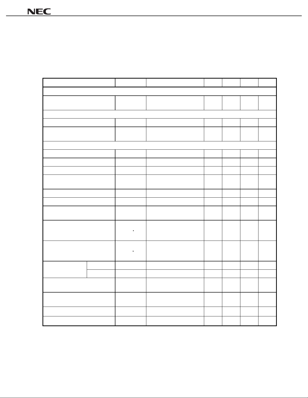
ELECTRICAL SPECIFICATIONS (1)
µµµµ
PC8139GR-7JH
TA = +25°C, VCC = 3.0 V, unless otherwise specified, V
= VCC/2 = 1.5 V, V
I/Qin
= 500 mV
P-P
(double phase input) , f
PS-TX/VAGC
= 3.0 V, V
I/Qin
Transmission rate: 384 kbps, Filter roll-off rate : α = 0.5, MOD pattern: all zero, f
MODLOin
P
= –7 dBm, f
TX
MIX-LOin
•
= 1673.4 MHz, P
TX
MIX-LOin
•
= –10 dBm, f
PS-RX
= 3.0 V (high), I/Q (DC) = Ib/Qb (DC)
= 24 kHz, π/4DQPSK modulated wave input
MOD
LOin
= 233.15 MHz,
•
TX
MIXout
= 1906.55 MHz + f
•
I/Qin
Parameter Symbol Condition MIN. TYP. MAX. Unit
Total characteristics
Total circuit current (TX + RX +
ICC
(TOTAL)
No signal input 33 40.5 49 mA
VCO)
Transmitter block total characteristics (quadrature modulator + up converter + AGC circuit)
Total circuit current (TX) ICC
Dark current at power save (TX) I
(TX-TOTAL)
CC (PS) TX-TOTALVPS
No signal input 27 32.5 39.5 mA
≤ 0.5 V (Low), No
–0.15µA
signal input
Transmitter block (quadrature modulator + up converter + AGC circuit)
Total output level P
TX • MIXout
Local carrier leak LOL f
AGC
V
= 3.0 V –17 –13 – dBm
MODin • LOin
TX • MIX-LOin
+ f
– –40 –30 dBc
Image rejection (side-band leak) ImR – –40 –30 dBc
I/Q 3rd order inter-modulation
IM
3 (I/Q)
– –50 –30 dBc
distortion
AGC circuit gain control range GCR V
AGC
= 3 V → 1 V 20 35 – dB
Error vector magnitude (vector error) EVM MOD pattern: PN 9 – 1.0 5 %rms
Adjacent channel leak power P
adj
f = ±600 kHz,
∆
– –68 –60 dBc
MOD pattern: PN 9
Spurious within transmission band 1 Pout
(7 MOD
LO)
MOD • LOin
f
MOD • LOin
f
= 259.25 MHz
MOD • LOin
× 7, f
× 7
– –65 –55 dBc
(Image)
Spurious within transmission band 2 Pout
(8 MOD
LO)
MOD • LOin
f
MOD • LOin
f
= 233.15 MHz
MOD • LOin
× 8, f
× 8
– –65 –55 dBc
(Image)
Rise time T
response time
Fall time T
I/Q input impedance Z
PS-TX (Rise)
PS-TX (Fall)
I/Q
PS-TX
V
= 0 V → 3 V –25µsPower saving
PS-TX
V
= 3 V → 0 V –25µs
Value between Pins I/Ib and
– 180 – k
Q/Qb
I/Q input bias current I
Power save low
Power save high
Note 1
Note 2
I/Q
PS-TX (Low)
V
PS-TX (High)
V
Value of each pin when
I
V
= VIb = VQ = V
Qb
3.5 7 16
0–0.5V
0.9 – V
CC
Ω
A
µ
V
Notes 1.
2.
Power save pin applied voltage in sleep mode
Power save pin applied voltage in active mode
Preliminary Data Sheet
5

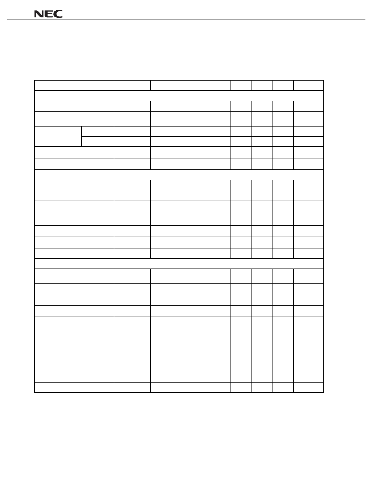
ELECTRICAL SPECIFICATIONS (2)
µµµµ
PC8139GR-7JH
TA = +25°C, VCC = 3.0 V, unless otherwise specified, VPS = 3.0 V (high), f
2ndMIX-LOin
f
2ndIFout
f
= 233.15 MHz, P
= 10.8 MHz
Parameter Symbol Condition MIN. TYP. MAX. Unit
Receiver block total characteristics
Total circuit current (RX) I
Dark current at power save I
Rise time T
response time
Power save low
Power save high
Fall time T
Note 1
Note 2
Receiver block 1 (2nd down converter)
2nd MIX conversion gain CG
1-dB compression output level P
Input 3rd order intercept point IIP3
2nd MIX noise figure NF
2nd MIX local leak 1 ISL
2nd MIX local leak 2 ISL
2ndMIX-LOin
CC (RX-TOTAL)
CC (PS-RX
TOTAL)
PS-RX (Rise)
PS-RX (Fall)
PS-RX (Low)
V
PS-RX (High)
V
1dB2ndMIX
= –7 dBm, f
2ndMIX
(2ndMIX)
2ndMIX
(2ndLO)1
(2ndLO)2
2ndMIXout
= 10.8 MHz, f
No signal input 3.5 4.8 6 mA
PS-RX
V
≤ 0.3 V (Low), No signal
input
VPS-RX = 0 V → 3 V – 2 5
VPS-RX = 3 V → 0 V – 2 5
Combining capacitance with SG 6 10 14 dB
2ndMIXin1
f
= 243.95 MHz,
2ndMIXin2
f
= 244.25 MHz
At I/O LC matching – 8 – dB
Pin 10 input –7-dBm input
Pin 10 input –7-dBm input
Note 3
Note 4
2ndMIXin
= 243.95 MHz, P
2ndIFin
= 10.8 MHz, P
2.5 – V
2ndMIXin
= –40 dBm,
2ndIFin
= –15 dBm,
–0.15µA
sPower save
µ
s
µ
0–0.3 V
CC
–93– dB
–94– dB
–52– dB
–24– dB
V
V
µ
V
µ
V
µ
V
µ
2nd MIX output resistance Z
2ndMIXout
Pin 20 – 330 –
Receiver block 2 (IF amplifier)
Limiting sensiti v ity S
2nd IF amplifier gain G
2nd IF amplifier phase shift S
2nd IF amplifier output amplitude V
2nd IF amplifier output
L
V
P
O
R
t
–3 dB point – 27 32 dBµVEM
2ndIFin
P
= 13 dBµVEMF – 80 – dB
2ndIFin
P
= 63 to 98 dBµVEMF
10 kΩ//10 pF
Note 6
Note 5
– 6 – deg
0.5 0.62 0.75 V
–1325 ns
rise time
2nd IF amplifier output
F
t
–1020 ns
fall time
2nd IF amplifier input resistance R
2nd IF amplifier input
in
in
C
Pin 16, Pin 17 – 330 –
Pin 16, Pin 17 – TBD – pF
capacitance
2nd IF amplifier output duty ratio VO (duty) – 52 – %
2nd IF amplifier output bias level VO (DC) – 1.5 – V
Notes 1.
Power save pin applied voltage in sleep mode
Power save pin applied voltage in active mode
2.
Leak to 2nd MIX output pin (Pin 20) of 2nd MIX-LO
3.
Leak to 2nd MIX input pin (Pin 22) of 2nd MIX-LO
4.
RBW of network analyzer = 3 Hz
5.
10 pF is a value including all capacitance connected to the pins (wiring pattern)
6.
Ω
F
P-P
Ω
6
Preliminary Data Sheet
 Loading...