NEC UPC8129GR-E1, UPC8129GR Datasheet

DATA SHEET
DATA SHEET
BIPOLAR ANALOG INTEGRATED CI RCUIT
µµµµ
PC8129GR
UP CONVERTER WITH AGC FUNCTION + QUADRATURE MODULATOR IC
FOR DIGITAL MOBILE COMMUNICATION SYSTEMS
DESCRIPTION
The µPC8129GR is a silicon monolithic integrated circuit designed as indirect quadrature modulator for digital
mobile communication systems. This modulator consists of 0.8 GHz to 1.9 GHz up-converter and 100 MHz to 400
MHz quadrature modulator which are packaged in 20 pin SSOP. The device has power save function and can
operate 2.7 to 5.5 V supply voltage, therefore, it can contribute to make RF block small, high performance and low
power consumption.
FEATURES
• High linearity up converter is incorporated; P
• Wide operating frequency range. Up converter; f
Modulator ; f
• External IF filter can be applied between modulator output and up converter input terminal.
• Low phase difference due to digital phase shifter is adopted.
• Supply voltage: VCC = 2.7 to 5.5 V
• Equipped with power save function.
• 20 pin SSOP suitable for high density surface mounting.
RFout
= –5 dBm TYP./@f
RFout
= 800 MHz to 1900 MHz
LO1in
= 200 MHz to 800 MHz
MODout
f
= 100 MHz to 400 MHz, f
RFout
= 900 MHz
I/Q
= DC to 10 MHz
APPLICATIONS
• Digital cellular phones (ex. GSM etc…)
• Digital cordless phones
ORDERING INFORMATION
PART NUMBER PACKAGE SUPPLYING FORM
µ
PC8129GR-E1 20 pin plastic SSOP
(225 mil)
To order evaluation samples, please contact your local NEC sales office. (Part number for sample order:
*
PC8129GR)
µ
Caution electro-static sensitive device
The information in this document is subject to change without notice. Before using this document, please
confirm that this is the latest version.
Not all devices/types available in every country. Please check with local NEC representative for
availability and additional information.
Embossed tape 12 mm wide. QTY 2.5 kp/Reel.
Pins 1 through 10 are in pull-out direction.
Document No. P12781EJ2V0DS00 (2nd edition)
Date Published October 1999 N CP(K)
Printed in Japan
The mark shows major revised points.
©
1997, 1999
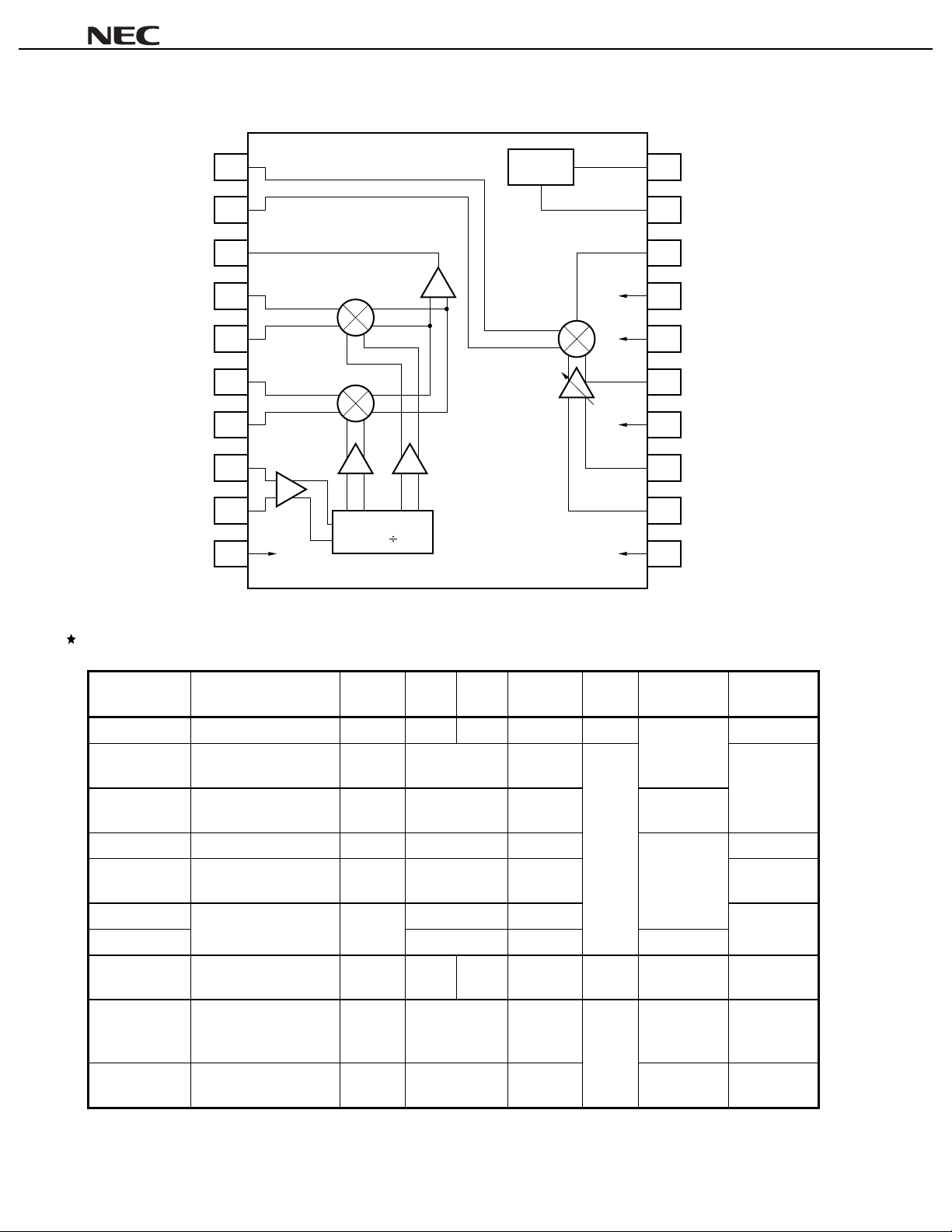
INTERNAL BLOCK DIAGRAM AND PIN CONNECTIONS
µµµµ
PC8129GR
Up-Con in
Up-Con inb
MODout
Qb
LO1 in
LO1 inb
GND
1
2
3
I
4
Ib
5
6
Q
7
8
9
10
90deg. Phase
Shifter ( 2)
Reg.
20
19
18
17
16
15
14
13
12
11
VCC (MOD)
V
CC
(Up-con)
RFout
GND
V
PS
V
AGC
GND
LO2 in
LO2 inb
GND
QUADRATURE MODULATOR SERIES PRODUCT
CC
Part Number Functions
PC8101GR 150 MHz Quad.Mod
µ
PC8104GR RF Up-Converter + IF
µ
I
(mA)
15/@2.7 V
28/@3.0 V
Quad.Mod
PC8105GR 400 MHz Quad.Mod
µ
PC8110GR 1 GHz Direct Quad.Mod
µ
PC8125GR RF Up-Converter + IF
µ
16/@3.0 V
24/@3.0 V
36/@3.0 V
Quad.Mod + AGC
PC8126GR 915 to 960 915 to 960
µ
PC8126K
µ
PC8129GR
µ
900 MHz Direct Quad.Mod
with Offset-Mixer
2LO IF Quad. Mod+RF
×
35/@3.0 V
28/@3.0 V
Up-Converter
µ
PC8139GR-7JH
PC8158K RF Up-Converter + IF
µ
Transceiver IC
(1.9 GHz Indirect Quad.
Mod + RX-IF + IF VCO)
TX: 32.5
RX: 4.8
/@3.0 V
28/@3.0 V
Quad.Mod + AGC
LO1in
f
(MHz)
100 to 300 50 to 150
MODout
f
(MHz)
100 to 400
RF Mixer
RFout
f
External F/F CT-2 etc.
900 to 1 900
100 to 400 External
800 to 1 000 External
220 to 270
1 800 to 2 000
889 to 960 889 to 960
200 to 800 100 to 400
220 to 270
100 to 300
800 to 1 900
1 800 to 2 000
800 to 1 500
(MHz)
Phase
Shifter
Doubler
+ F/F
F/F
CR
Package Application
20-pin
SSOP (225 mil)
Digital Comm.
16-pin
SSOP (225 mil)
20-pin
SSOP (225 mil)
PDC800 MHz, etc.
PHS
PDC800 MHz
28-pin QFN
20-pin
SSOP (225 mil)
30-pin
GSM,
DCS1800, etc.
PHS
TSSOP (225 mil)
28-pin QFN
PDC800 M/1.5 G
2
Data Sheet P12781EJ2V0DS00
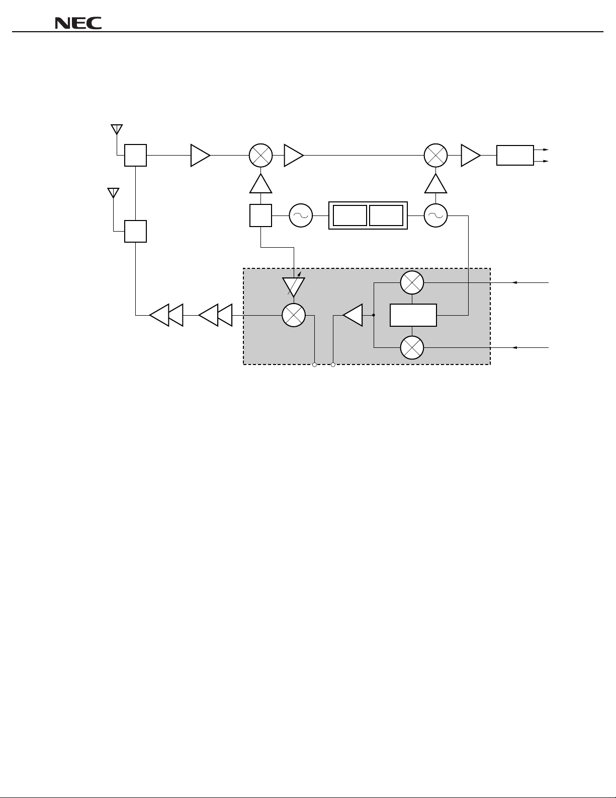
APPLICATION EXAMPLE
[GSM]
SUB ANT
µµµµ
PC8129GR
MAIN ANT
TX
SW
SW
RX
LNA 1st MIX
PA
SW
AGC
1st. LO
PLL1 PLL2
MODout
= f
LO
/2
(F/F)
φ
2nd MIX
2nd. LO
0 °
90 °
PC8129GR
µ
DEMO.
LO
f
I
Q
I
Q
Data Sheet P12781EJ2V0DS00
3
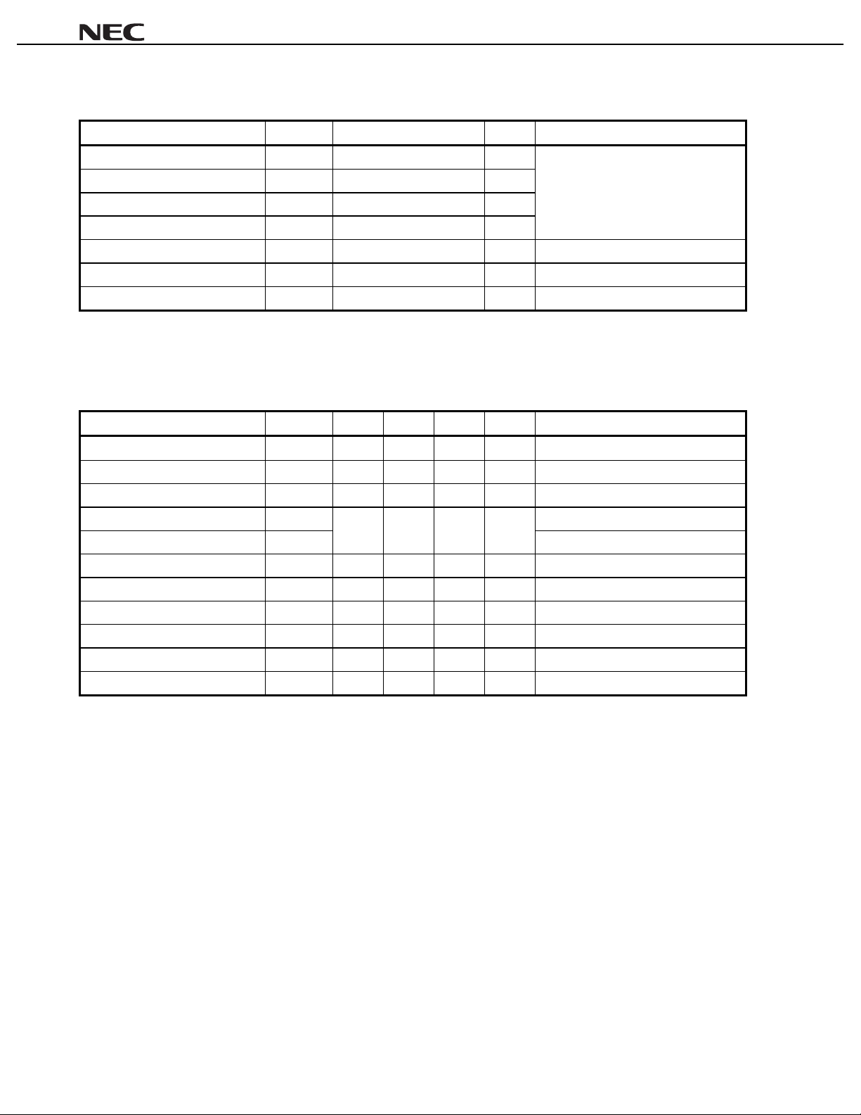
ABSOLUTE MAXIMUM RATINGS
PARAMETER SYMBOL RATING UNIT CONDITION
µµµµ
PC8129GR
Supply Voltage V
Power Save Voltage V
AGC Control Voltage V
CC
PS
AGC
6.0 V TA = +25 °C
6.0 V
6.0 V
IQ DC Offset Voltage IQ (DC) 4.0 V
Power Dissipation P
Operating Ambient Temperature T
Storage Temperature T
Mounted on double sided copper clad 50 × 50 × 1.6 mm epoxy glass PWB.
Note
D
A
stg
430 mW
–40 to +85 °C
–55 to +150 °C
RECOMMENDED OPERATING CONDITIONS
PARAMETER SYMBOL MIN. TYP. MAX. UNIT CONDITIONS
Supply Voltage V
Operating Ambient Temperature T
Up Converter RF Frequency f
Up Converter Input Freq. f
Modulator Output Frequency f
LO1 Input Frequency f
LO1 Input Level P
LO2 Input Frequency f
LO2 Input Level P
I/Q Input Frequency f
I/Q Input Amplitude V
CC
A
RFout
UPCONin
MODout
LO1in
LO1in
LO2in
LO2in
I/Qin
I/Qin
2.7 3.0 5.5 V
–40 +25 +85 °C
800 1900 MHz
100 400 MHz
200 800 MHz
–15 –10 –5 dB m
800 1800 MHz
–15 –10 –5 dB m
DC 10 M Hz
600 mV
A
= +85 °C
T
P-P
Single ended Input
Note
4
Data Sheet P12781EJ2V0DS00
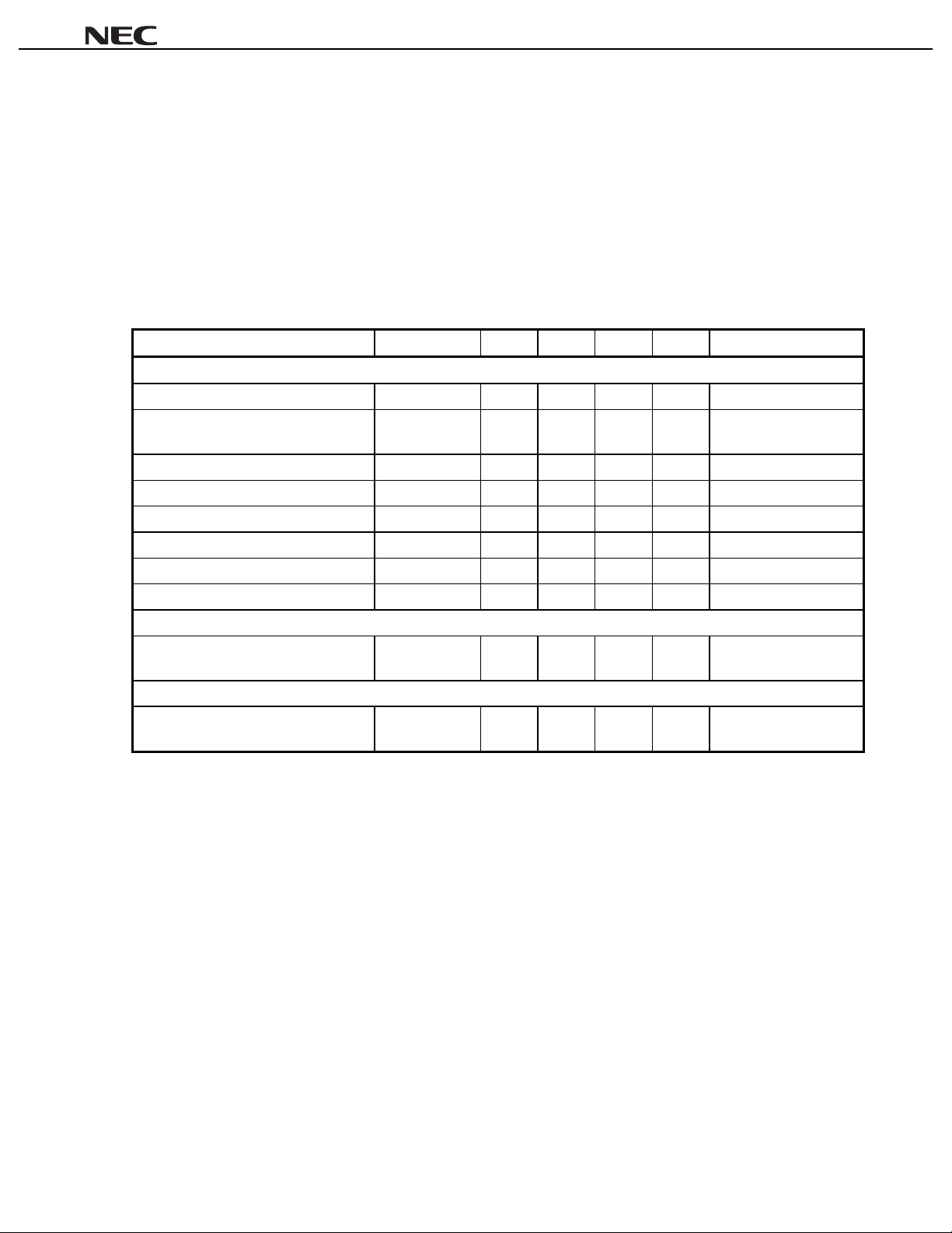
ELECTRICAL CHARACTERISTICS (1)
Conditions (unless otherwise specified):
TA = +25 °C, VCC = 3 V, VPS = 3 V, RPS = 1 kΩ, V
AGC
= 3 V, R
I/Q DC = 1.5 V (Vbias(I) = Vbias(Ib) = Vbias (Q) = Vbias (Qb) = 1.5 V)
I/Qin
f
= 67.7 kHz, V
I/Qin
= 500 mV
P-P
(single ended input, Ib = Qb = 0 mV
Modulation Pattern: <0000>
LO1in
f
= 500 MHz, P
LO2in
f
= 1150 MHz, P
UPCONin
f
RFout
f
MODout
= f
= 900 MHz – f
PARAMETER SYMBOL MIN. TYP. MAX. UNIT TEST CONDITIONS
UP CONVERTER + QUADRATURE MODULATOR TOTAL
Total Circuit Current I
Total Circuit Current at Power S ave
Mode
Total Output Power P
Local Oscillator Carrier Leakage LoL –40 –26.5 dBc f
Image Rejection (Side Band Leak ) ImR –30 –26.5 dBc
AGC Gain Control Rang GCR 28 40 dB V
Power Save Rise Time TPS(rise) 2.0 5.0
Power Save Fall Time TPS(fall) 2.0 5.0
UP CONVERTER BLOCK
Circuit Current at Power Save Mode I
QUADRATURE MODULATOR BLOCK
Circuit Current at Power Save Mode I
= f
LO1in
= –10 dBm
LO2in
= –10 dBm
LO1in
/2 + f
I/Qin
I/Qin
= 250 MHz + f
CC(TOTAL)
CC(PS)TOTAL1
I
(Up con.)
(MOD)
RFout
CC(PS)
CC(PS)
I/Qin
20 28 37 mA No input signal
–8 –5 –2 dBm
AGC
= 10 k
0.6 10
Ω
P-P
5.0
5.0
)
AVPS ≤ 0.5 V
µ
sVPS(Low) → VPS(High)
µ
sVPS(High) → VPS(Low)
µ
AVPS ≤ 0.5 V
µ
AVPS ≤ 0.5 V
µ
µµµµ
PC8129GR
LoL
LO2
= f
AGC
LO1
– f
/2
= 2.5 V to 0 V
Data Sheet P12781EJ2V0DS00
5
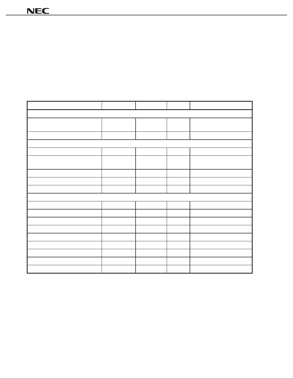
STANDARD CHARACTERISTICS FOR REFERENCE (1)
Conditions (unless otherwise specified):
TA = +25 °C, VCC = 3 V, VPS = 3 V, RPS = 1 kΩ, V
AGC
= 3 V, R
I/Q DC = 1.5 V (Vbias(I) = Vbias(Ib) = Vbias (Q) = Vbias (Qb) = 1.5 V)
I/Qin
f
= 67.7 kHz, P
I/Qin
= 500 mV
P-P
(single ended input, Ib = Qb = 0 mV
Modulation Pattern: <0000>
LO1in
f
= 500 MHz, P
LO2in
f
= 1150 MHz, P
UPCONin
f
RFout
f
MODout
= f
= 900 MHz – f
PARAMETER SYMBOL REFERENCE UNIT TEST CONDITIONS
UP CONVERTER + QUADRATURE MODULATOR TOTAL
Total Circuit Current at Power-S ave
Mode
Phase Error
UP CONVERTER BLOCK
UP Con. Circuit Current I
UP Con. Circuit Current at Power-Save
Mode
Conversion Gain CG 12 dB P
Maximum Output Power P
Output 3rd Order Intercept Point OIP
QUADRATURE MODULATOR BLOCK
MOD. Circuit Current I
Output Power P
LO1 Carrier Leakage LoL –40 dBc f
Image Rejection (Side Band Leak ) ImR –30 dBc
I/Q 3rd Order Intermodulation Dis tortion IM
I/Q Input Impedance Z
IQ Bias Current I
LO1 Input VSWR VSWR
Output Noise Floor –133 dB c /Hz
= f
LO1in
= –10 dBm
LO2in
= –10 dBm
LO1in
/2 + f
I/Qin
I/Qin
= 250 MHz + f
CC(PS)TOTAL2
I
CC(PS)UpCon
I
I/Qin
∆φ
CC(UpCon)
RF(sat)
3
CC(MOD)
MODout
3I/Q
I/Q
I/Q
(Lo1)
AGC
= 10 k
Ω
P-P
)
60
AVPS ≤ 0.5 V, V
µ
1.8 deg. (rms) MOD Pattern: PN9
14 mA No input signal
60
AVPS ≤ 0.5 V, V
µ
–1.5 dBm P
+6 dBm f
14 mA No input signal
–16.5 dBm
–50 dBc
200 k
5
Ω
A I, Ib, Q, Qb to GND (each)
µ
1.2 : 1 –
AGC
AGC
UPCONin
= –20 dBm
UPCONin
= –4 dBm
UPCONin
= 250.0 MHz/250.2 MHz
LoL
LO1
= f
/2
I to Ib, Q to Qb
f = ±20 MHz
∆
µµµµ
PC8129GR
= 0 V
= 0 V
6
Data Sheet P12781EJ2V0DS00
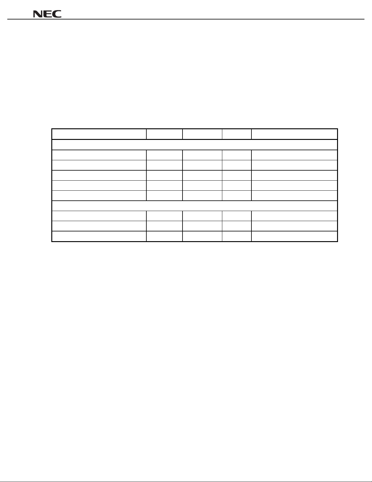
STANDARD CHARACTERISTICS FOR REFERENCE (2)
Conditions (unless otherwise specified):
TA = +25 °C, VCC = 3 V, VPS = 3 V, RPS = 1 kΩ, V
AGC
= 3 V, R
I/Q DC = 1.5 V (Vbias(I) = Vbias(Ib) = Vbias (Q) = Vbias (Qb) = 1.5 V)
I/Qin
f
= 67.7 kHz, P
I/Qin
= 500 mV
P-P
(single ended input, Ib = Qb = 0 mV
Modulation Pattern: <0000>
LO1in
f
= 500 MHz, P
LO2in
f
= 1650 MHz, P
UPCONin
f
RFout
f
MODout
= f
= 1900 MHz + f
PARAMETER SYMBOL REFERENCE UNIT TEST CONDITIONS
UP CONVERTER + QUADRATURE MODULATOR TOTAL
Total Output Power P
Local Oscillator Carrier Leakage LoL –40 dBc f
Image Rejection (Side Band Leak ) ImR –30 dB c
AGC Gain Control Rang GCR 45 dB V
Phase Error
UP CONVERTER BLOCK
Conversion Gain CG 5 dB P
Maximum Output Power P
Output Intercept Point OIP
= f
LO1in
= –10 dBm
LO2in
= –10 dBm
LO1in
/2 + f
I/Qin
I/Qin
= 250 MHz + f
I/Qin
RFout
∆φ
RF(sat)
3
AGC
= 10 k
Ω
P-P
–12 dBm
1.8 deg. (rms) MOD Pattern: PN9
–7 dBm P
–1 dBm f
µµµµ
PC8129GR
)
LoL
LO2
= f
AGC
UPCONin
UPCONin
UPCONin
LO1
+ f
/2
= 2.5 V to 0 V
= –20 dBm
= –4 dBm
= 250.0 MHz/250.2 MHz
Data Sheet P12781EJ2V0DS00
7
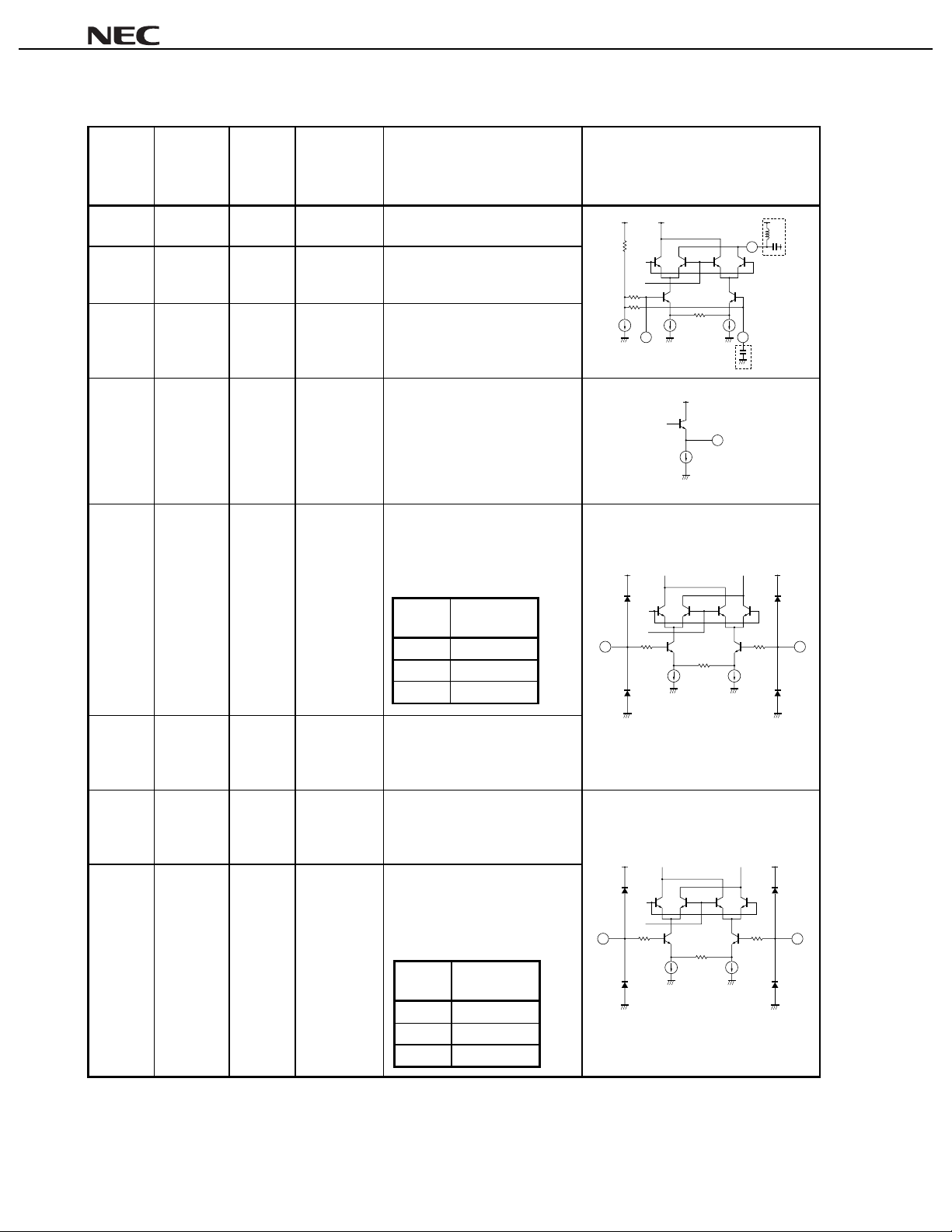
PIN EXPLANATION
µµµµ
PC8129GR
Pin
Voltage
Description Equivalent Circuit
Typ. (V)
CC
@V
= 3 V
CC
– RF output from Up-Converter.
Pin No. Symbol
18 RFout V
Supply
Voltage
(V)
This pin is open collect or out put.
1 UpCon in – 2.2 IF input for Up-converte r.
This pin is high impedance
input.
2 UpCon inb – 2.2 Bypass of IF input .
Grounded through external
capacitor.
3 MODout – 1.9 Output from modulator.
This is emitter follower output.
4IV
CC
/2 – Input for I signal. This input
impedance is about 200 kΩ.
Relations between amplitude
CC
and V
/2 bias of input signal
are following.
CC
/2
(V)
1.5
Signal Level
(mV
≤
≤
1000
≤
V
1.35
≥
≥
1.75
≥
P-P
400
600
18
1 2
3
Note
)
4 5
5IbV
CC
/2 – Input for I signal. This input
impedance is about 200 kΩ.
CC
V
/2 biased DC signal should
be input.
6QbV
CC
/2 – Input for Q signal. This i nput
impedance is about 200 k
CC
/2 biased DC signal should
V
Ω
be input.
7QV
CC
/2 – Input for Q signal. This i nput
impedance is about 200 kΩ.
Relations between amplitude
CC
and V
/2 bias of input signal
are following.
In the case of that I/Q input signals are single ended.
Note
VCC/2
(V)
1.35
≥
≥
1.75
≥
1.5
Signal Level
P-P
(mV
)
400
≤
600
≤
1000
≤
Note
Of course, I/Q signal inputs can be used either single endedly or differentially with proper terminations.
67
8
Data Sheet P12781EJ2V0DS00
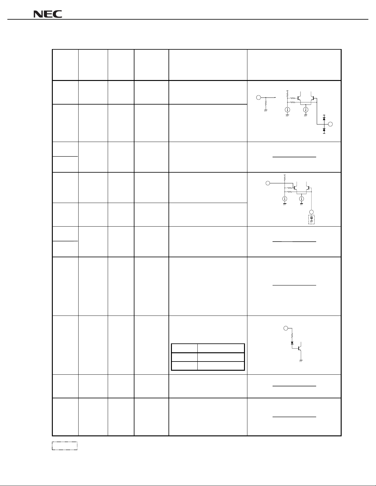
PIN EXPLANATION
µµµµ
PC8129GR
Pin
Voltage
Typ. (V)
CC
@V
Description Equivalent Circuit
= 3 V
Pin No. Symbol
Supply
Voltage
(V)
8 LO1in – 0 Lo1 input for phase shifter.
This input impedance is 50
matched internally.
9 LO1in b – 2.3 Bypass of Lo1 input.
This pin is grounded through
internal capacitor.
10
11
GND for
Modulator
0 – Connect to the ground with
minimum inductance.
Track length should be kept as
short as possible.
12 LO2in b – 1. 9 Bypass of Lo2 input.
Grounded through external
capacitor.
13 LO2i n – 1.9 Lo2 input of Up-converter.
This pin is high impedance input.
14
17
GND for
Up-con.
0 – Connect to the ground with
minimum inductance.
Track length should be kept as
short as possible.
15 V
AGC
0 to V
CC
– Input for AGC amplifier.
Total Output Power can be
controlled by changing input
voltage.
And as external series resistance
AGC
(R
) connecting, a slope of
AGC curve can be changed by
AGC
16 Power
Save
0 to V
the resistance (R
CC
– Power save control pin can be
controlled ON/OFF state with
bias as follows;
Ω
8
50 Ω
9
13
12
).
16
19 VCC for
Upconverter
20 VCC for
Modulator
: Externally
VPS (V) STATE
2 to VCCON (Active Mode)
0 to 0.5 OFF (Sleep Mode)
2.7 to 5.5 – Supply voltage pin for Upconverter.
2.7 to 5.5 – Supply voltage pin for modulator.
Internal regulator can be kept
stable condition of suppl y bias
against the variable
temperature or V
Data Sheet P12781EJ2V0DS00
CC
.
9
 Loading...