NEC UPC8125GR, UPC8125GR-E1 Datasheet

DATA SHEET
BIPOLAR ANALOG INTEGRATED CI RCUIT
µµµµ
PC8125GR
UP-CONVERTER WITH AGC FUNCTION
QUADRATURE
++++
MODULATOR IC FOR DIGITAL MOBILE COMMUNICATION SYSTEMS
DESCRIPTION
The µPC8125GR is a sillicon monolithic integrated circuit designing as indirect quadrature modulator for digital
mobile communication systems. This modulator consists of 1.8 GHz to 2.0 GHz up-converter with AGC function and
220 MHz to 270 MHz quadrature modulator which are packaged in 20-pin SSOP. The device has power save
function and can operate 2.7 to 5.5 V supply voltage. Therefore, it can contribute to make RF block small, high
performance and low power consumption.
FEATURES
• LPF is incorporated in the latter of 90° phase shifter for Lo1 Carrier leak and its Lo1 × n spurious level.
• Supply voltage: VCC = 2.7 to 5.5 V
• External IF filter can be applied between modulator output and up-converter input terminal.
• Equipped with power save function.
• Equipped with AGC function : Gain control range 40 dB TYP. @f = 1.9 GHz
APPLICATIONS
• Digital cordless phones: ex) PHS (Personal Handy Phone System)
ORDERING INFORMATION
Part Number Package Supplying Form
µ
PC8125GR-E1 20 pin plastic SSOP (225 m i l ) E m bossed tape, 12 mm wide.
Remark
Document No. P11486EJ2V0DS00 (2nd edition)
Date Published November 1999 N CP(K)
Printed in Japan
To order evaluation samples, please contact your local NEC sales office.
(Part number for sample order:
The information in this document is subject to change without notice. Before using this document, please
confirm that this is the latest version.
Not all devices/types available in every country. Please check with local NEC representative for
availability and additional information.
Pins 1 through 10 are in pull-out directi on.
Qty 2.5 kp/reel.
PC8125GR, Quantity: 20 pcs/unit)
µ
Caution Electro-static sensitive device
The mark shows major revised points.
©
1997, 1999
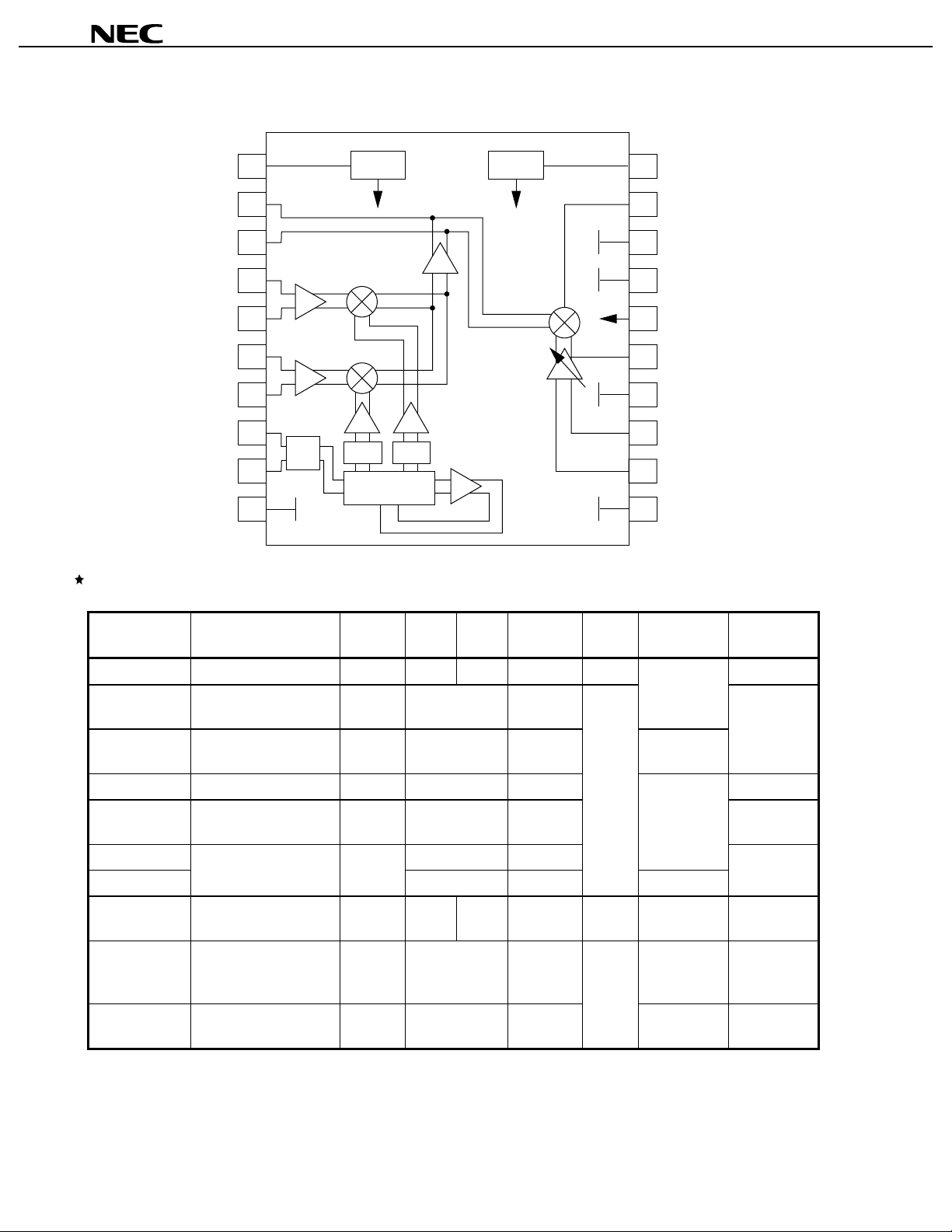
INTERNAL BLOCK DIAGRAM AND PIN CONNECTIONS (Top View)
V
CC
(MOD)
1
Reg. Reg.
20
CC
(Up-con.)
V
µµµµ
PC8125GR
Filter1
Filter2
Lo1 in
Lo1 inb
Qb
2
3
I
4
Ib
5
Q
6
7
8
× 2
9
LPF LPF
90 deg. Phase
Shifter (÷2)
GND
10
QUADRATURE MODULATOR SERIES PRODUCT
Part Number Functions
CC
I
(mA)
LO1in
f
(MHz)
MODout
f
(MHz)
RF Mixer
RFout
f
(MHz)
Phase
Shifter
RF
out
19
GND
18
GND
17
PS
V
16
V
AGC
15
GND
14
Lo2 in
13
Lo2 inb
12
GND
11
Package Application
PC8101GR 150 MHz Quad.Mod
µ
PC8104GR RF Up-Converter + IF
µ
15/@2.7 V
28/@3.0 V
100 to 300 50 to 150
100 to 400
External F/F CT-2 etc.
900 to 1 900
Quad.Mod
PC8105GR 400 MHz Quad.Mod
µ
PC8110GR 1 GHz Direct Quad.Mod
µ
PC8125GR RF Up-Converter + IF
µ
16/@3.0 V
24/@3.0 V
36/@3.0 V
100 to 400 External
800 to 1 000 External
220 to 270
1 800 to 2 000
Quad.Mod + AGC
PC8126GR 915 to 960 915 to 960
µ
PC8126K
µ
PC8129GR
µ
900 MHz Direct Quad.Mod
with Offset-Mixer
2LO IF Quad. Mod+RF
×
35/@3.0 V
28/@3.0 V
889 to 960 889 to 960
200 to 800 100 to 400
800 to 1 900
Up-Converter
µ
PC8139GR-7JH
PC8158K RF Up-Converter + IF
µ
Transceiver IC
(1.9 GHz Indirect Quad.
Mod + RX-IF + IF VCO)
TX: 32.5
RX: 4.8
/@3.0 V
28/@3.0 V
220 to 270
100 to 300
1 800 to 2 000
800 to 1 500
Quad.Mod + AGC
Remark
Please refer to the data sheet of each part number.
Doubler
+ F/F
F/F
CR
20-pin
SSOP (225 mil)
16-pin
SSOP (225 mil)
20-pin
SSOP (225 mil)
28-pin QFN
20-pin
SSOP (225 mil)
30-pin
TSSOP (225 mil)
28-pin QFN
Digital Comm.
PDC800 MHz, etc.
PHS
PDC800 MHz
GSM,
DCS1800, etc.
PHS
PDC800 M/1.5 G
2
Data Sheet P11486EJ2V0DS00
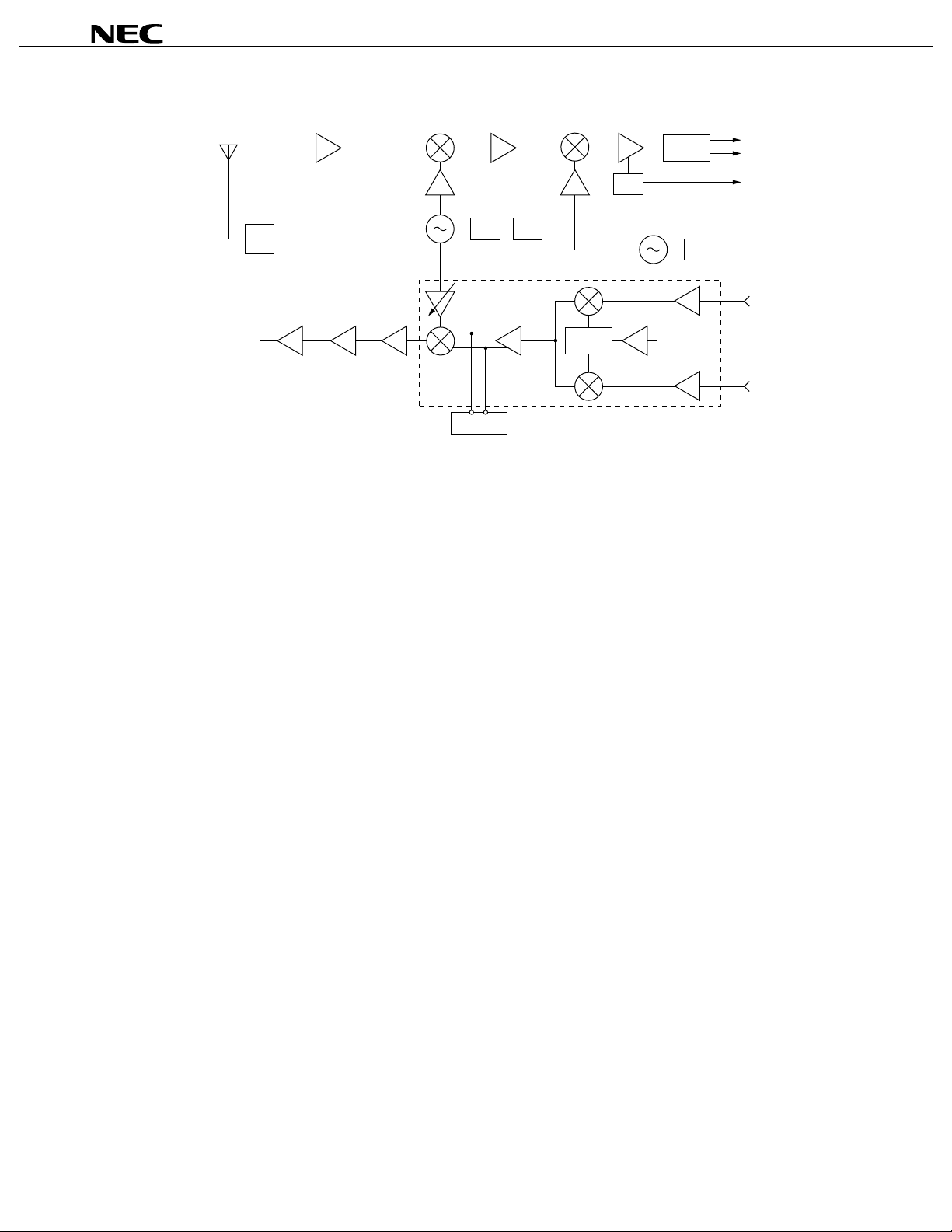
APPLICATION EXAMPLE (PHS)
µµµµ
PC8125GR
RX
TX
SW
PA
÷N
LC Filter
PLL
µ
PC8125GR
φ
0°
90°
DEMO.
PLL
I
Q
RSSI
I
Q
Data Sheet P11486EJ2V0DS00
3

µµµµ
PC8125GR
CONTENTS
1. ABSOLUTE MAXIMUM RATINGS................................................................................................. 5
2. RECOMMENDED OPERATING CONDITIONS ............................................................................ 5
3. ELECTRICAL CHARACTERISTICS.............................................................................................. 6
4. STANDARD CHARACTERISTICS FOR REFERENCE............................................................... 6
5. PIN EXPLANATIONS ..................................................................................................................... 7
6. RELATIONS BETWEEN AMPLITUDE AND V
7. STANDARD TYPICAL CHARACTERISTICS ............................................................................... 10
7.1 DC Performance................................................................................................................... 11
7.2 Output Performance ............................................................................................................ 12
7.3 Adjacent Channel Interference Power ............................................................................... 14
7.4 Error and Accuracy.............................................................................................................. 15
7.5 Power Save Response Time ............................................................................................... 16
7.6 Spectrum............................................................................................................................... 18
7.7 Input/output Impedance ...................................................................................................... 19
8. TEST CIRCUIT (SINGLE ENDED INPUT) .................................................................................. 20
9. APPLICATION CIRCUIT EXAMPLE (IN THE CASE OF SINGLE ENDED INPUT).............. 21
10. ASSEMBLED TEST BOARD ........................................................................................................ 22
11. PACKAGE DIMENSIONS............................................................................................................... 23
12. NOTE ON CORRECT USE........................................................................................................... 24
CC
/2 BIAS OF I/Q INPUT SIGNALS ............. 9
13. RECOMMENDED SOLDERING CONDITIONS ............................................................................ 24
4
Data Sheet P11486EJ2V0DS00
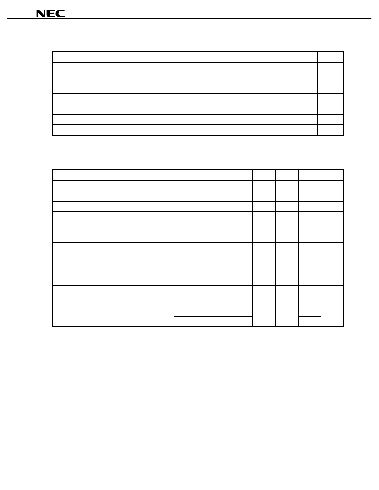
1. ABSOLUTE MAXIMUM RATINGS
Parameter Symbol Conditions Rating Unit
µµµµ
PC8125GR
Supply Voltage V
Power Save Control Voltage V
AGC Control Voltage V
IQ DC Offset Voltage IQ
Power Dissipation P
Operating Ambient Temperature T
Storage Temperature T
Mounted on a 50 × 50 × 1.6 mm double copper clad epoxy glass PWB.
Note
CC
PS
AGC
(DC)
stg
TA = +25 °C 6.0 V
TA = +25 °C 6.0 V
TA = +25 °C 6.0 V
TA = +25 °C, 4 to 7 pins 4.0 V
D
A
TA = +85 °C
2. RECOMMENDED OPERATING CONDITIONS
Parameter Symbol Test Conditions MIN. TYP. MAX. Unit
Supply Voltage V
Operating Ambient Temperature T
Up-converter RF Frequency f
Up-converter Input Frequency f
Modulator Output Frequency f
Lo1 Input Frequency f
Lo2 Input Frequency f
I/Q Input Frequency f
Lo1 Input Level P
Lo2 Input Level P
I/Q Input amplitude V
CC
A
RFout
UPCONin
MODout
Lo1in
Lo2in
I/Qin
Lo1in
Lo2in
I/Qin
Lo1in
P
= −10 dBm
Lo2in
P
= −10 dBm 1 500
I/Qin
V
= 500 mVp-p max.
(Single ended Input)
I/Qin
= 250 mVp-p max.
V
(Differential Input)
Single ended Input
Differential Input 250
Note
430 mW
40 to +85
−
55 to +150
−
2.7 3.0 5.5 V
40
−
1 800
220
DC
11.5
−
15
−
−−
25
+
−
−
−
−
10
−
10
−
85
−
2 000 MHz
270 MHz
1 800 MHz
10 M Hz
5dBm
−
5dBm
−
500 mVp-p
C
°
C
°
C
°
Data Sheet P11486EJ2V0DS00
5
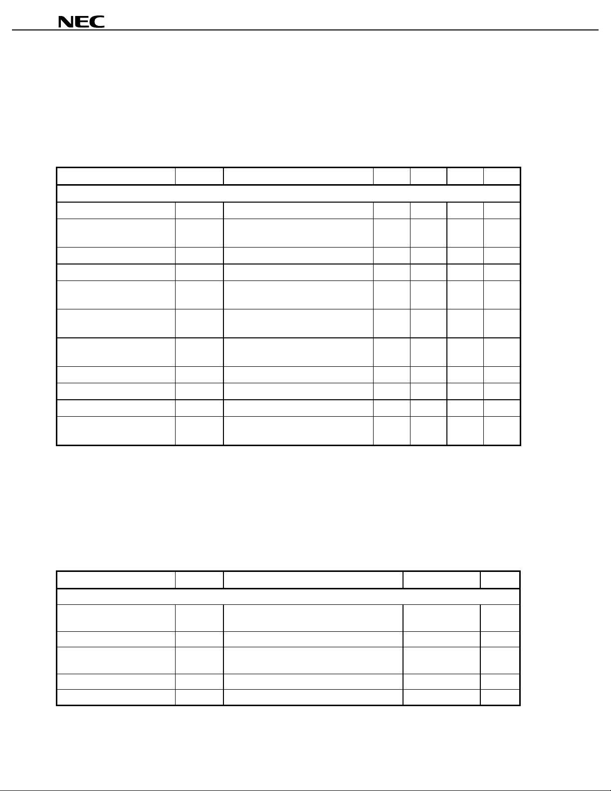
3. ELECTRICAL CHARACTERISTICS
µµµµ
PC8125GR
(TA = +25 °C, VCC = 3.0 V, unless otherwise specified V
I/Q (DC) = Ib/Qb (DC) = VCC/2 = 1.5 V, f
V
= 500 mVp-p (Single ended) or 250 mVp-p (Differential Input), π/4DQPSK modulation,
I/Qin
= 24 kHz,
I/Qin
Data rate: 384 kbps, Filter roll off: α = 0.5, MOD pattern: all zero [0000], f
f
= 1 650 MHz, P
Lo2in
= −10 dBm, f
Lo2in
= 1 900 MHz + f
RFout
AGC
= 3.0 V, Vps = 3.0 V, R
)
I/Qin
= 250 MHz, P
Lo1in
Parameter Symbol Test Conditions MIN. TYP. MAX. Unit
UP-CONVERTER + QUADRATURE MODULATOR TOTA L
Total Circuit Current ICC
Total Circuit Current at
TOTAL
CC(PS) TOTALVPS
I
No input signal 30 36 48 mA
≤ 0.5 V (Low)
Sleep Mode
Total Output Power 1 P
RFout 1
Lo Carrier Leakage LoL f
Image Rejection
ImR
V
Lo1
AGC
+ f
= 3.0 V
Lo2
(Side Band Leakage)
I/Q 3rd Order Intermodulation
IM
3(I/Q)
Distortion
AGC Amp. Gain control
GCR V
AGC
= 2.5 V to 0 V 28 40
range
Power Save Rise Time T
Power Save Fall Time T
PS(Rise)
PS(Fall)
PS(Low)
V
PS(Low)
V
→ V
→ V
PS(High)
PS(High)
Error Vector Magnitude EVM MOD Pattern: PN9
Adjacent Channel Power P
adj
f = 600 kHz
∆
MOD Pattern: PN9
AGC
= 10 kΩ, Rps = 1 kΩ,
= −10 dBm,
Lo1in
−
13
−
0.3 10
9
−
−−37−
−−35−
−−50−
−
−
−
25
510
2.5 4.5 %rms
−−68−
A
µ
5dBm
−
30 dBc
30 dBc
30 dBc
−
dB
s
µ
s
µ
60 dBc
4. STANDARD CHARACTERISTICS FOR REFERENCE
(TA = +25 °C, VCC = 3.0 V, unless otherwise specified V
I/Q (DC) = Ib/Qb (DC) = VCC/2 = 1.5 V, f
V
= 500 mVp-p (Single ended) or 250 mVp-p (Differential Input), π/4DQPSK modulation,
I/Qin
= 24 kHz,
I/Qin
Data rate: 384 kbps, Filter roll off: α = 0.5, MOD pattern: all zero [0000], f
f
= 1 650 MHz, P
Lo2in
Parameter Symbol Test Conditions Reference Unit
UP-CONVERTER + QUADRATURE MODULATOR TOTA L
Lo1 × n Spurious Level P
Total Output Power P
I/Q Input Inpedance Z
I/Q Bias Current I
Lo1 Input VSWR Z
6
= −10 dBm, f
Lo2in
= 1 900 MHz + f
RFout
SUP(Lo1)
RFout 2
I/Qin
I/Q
Lo1in
Lo1 × 7, Lo1 × 7 (Image)
Lo1 × 8, Lo1 × 8 (Image)
AGC
V
= 0.5 V
I/Qin
f
= 24 kHz,
I to Ib, Q to Qb
I, Ib, Q, Qb to GND (each) 5
Lo1
f
= 220 M to 270 MHz 1.2:1
Data Sheet P11486EJ2V0DS00
AGC
= 3.0 V, Vps = 3.0 V, R
)
I/Qin
= 250 MHz, P
Lo1in
AGC
= 10 kΩ, Rps = 1 kΩ,
= −10 dBm,
Lo1in
60 dBc
−
50 dBm
−
200 k
Ω
A
µ
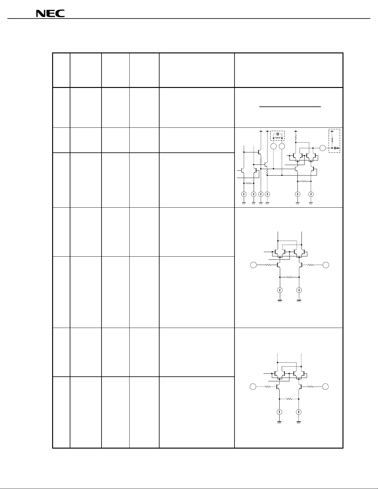
5. PIN EXPLANATIONS
µµµµ
PC8125GR
Pin
NO.
Symbol
Supply
Voltage
(V)
1VCC(MOD.) 2. 7 to
5.5
2 Filter1
3 Filter2
4IV
5IbV
6QV
7QbV
−
−
CC
/2
CC
/2
CC
/2
CC
/2
Pin
Voltage
Function and Description Internal Equivalent Circuit
Typ. (V)
CC
= 3 V
@V
−
Supply voltage pin for the
modulator. Internal regulator
can be kept stable condit i on
of supply bias against the
variable temperature or V
1.9 Filter pin can control
spurious (Lo1 × n) by insertion
BPF between Filter2 pin.
1.9 Filter pin can control
spurious (Lo1 × n) by insertion
BPF between Filter1 pin.
−
Input for I signal. This input
impedance is 200 kΩ. In case
of that I/Q input si gnal s are
single ended, amplitude of the
signal is 500 mVp-p max.
See
−
Input for I signal. This input
impedance is 200 kΩ. In case
of that I/Q input si gnal s are
single ended, V
signal should be input. In
case of the I/Q input signals
are differential, amplit ude of
the signal is 250 mVp-p max .
See
−
Input for Q signal. This i nput
impedance is 200 kΩ. In case
of that I/Q input si gnal s are
single ended, amplitude of the
signal is 500 mVp-p max.
See
−
Input for I signal. This input
impedance is 200 kΩ. In case
of that I/Q input si gnal s are
single ended, V
signal should be input. In
case of the I/Q input signals
are differential, amplit ude of
the signal is 250 mVp-p max .
See
Chapter 6
CC
/2 biased DC
Chapter 6
Chapter 6
CC
/2 biased DC
Chapter 6
CC
.
3192
.
2.1 k
2.1 k
54
2 k
.
.
2.1 k
6 7
2.1 k
2 k
.
Data Sheet P11486EJ2V0DS00
7
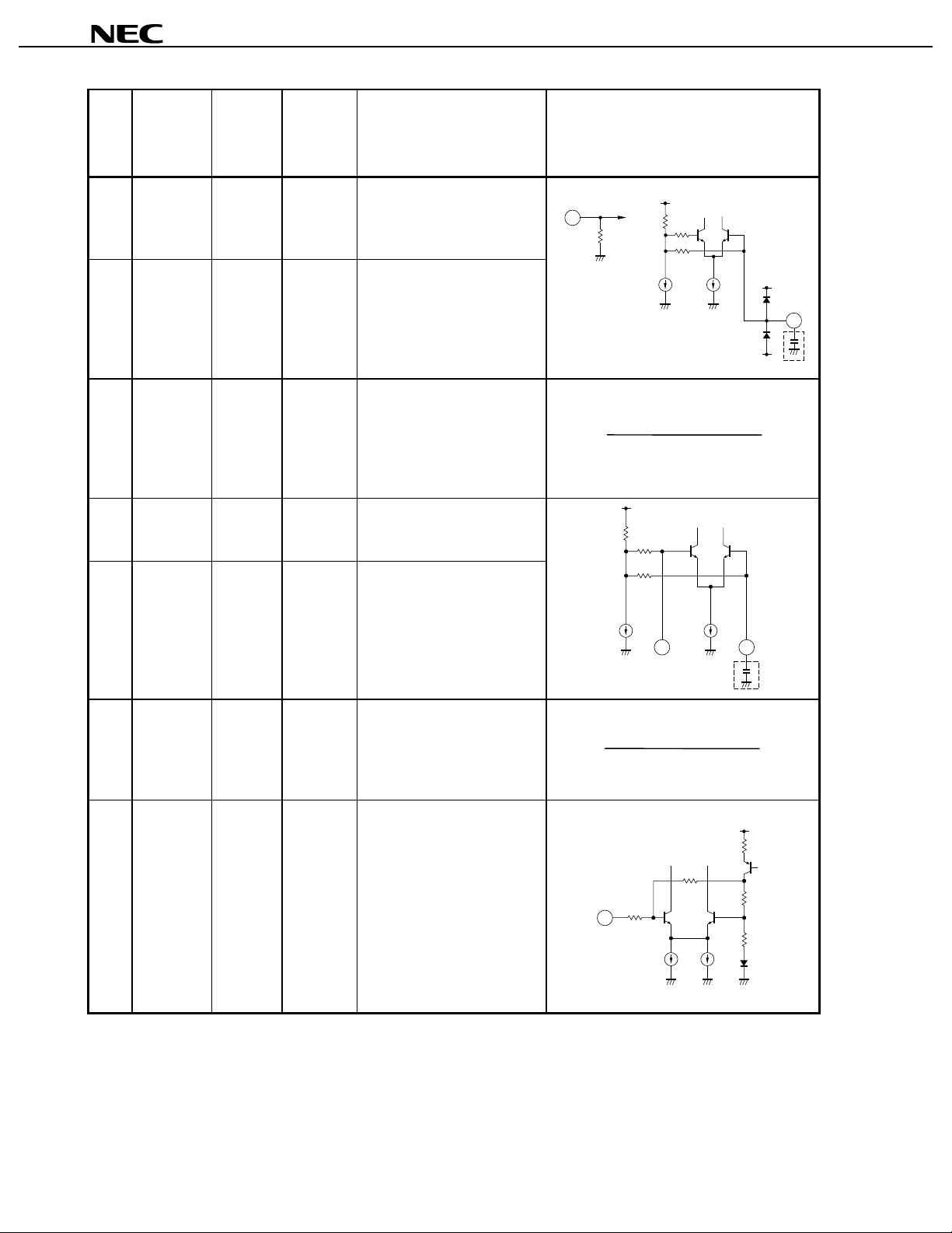
µµµµ
13 12
15
15 k
15 k
1 k
1 k
9 k
PC8125GR
Pin
NO.
Symbol
8 Lo1 in
9 Lo1 inb
10
11
12 Lo2 inb
13 Lo2 in
GND
(MOD.)
Supply
Voltage
(V)
−
−
−
−
−
Pin
Voltage
Typ. (V)
CC
= 3 V
@V
0 Lo input for the phase shi fter.
2.4 Bypass of the Lo1 input.
0 Ground pin for modulator
1.9 Bypass of the Lo2 input.
1.9 Lo input for the up-converter.
Function and Description Internal Equivalent Circuit
This input impedance is
internally matched to 50 Ω.
This pin is grounded through
external capacitor.
block. Connect to the ground
with minimum inductanc e.
Track length should be kept as
short as possible.
This pin is grounded through
external capacitor.
This pin is high impedance
input, and should be matched
external circuit.
8
50
9
14
17
18
15 V
8
GND
(Up-con.)
AGC
−
0 to V
0 Ground pin for up-Converter.
Connect to the ground with
minimum impedance.
Track length should be kept as
short as possible.
CC
−
Control voltage input pin for
AGC amplitude. RF output
level can be governed by
supply voltage to this pin.
AGC performance can be
AGC
adjustable R
Data Sheet P11486EJ2V0DS00
value.
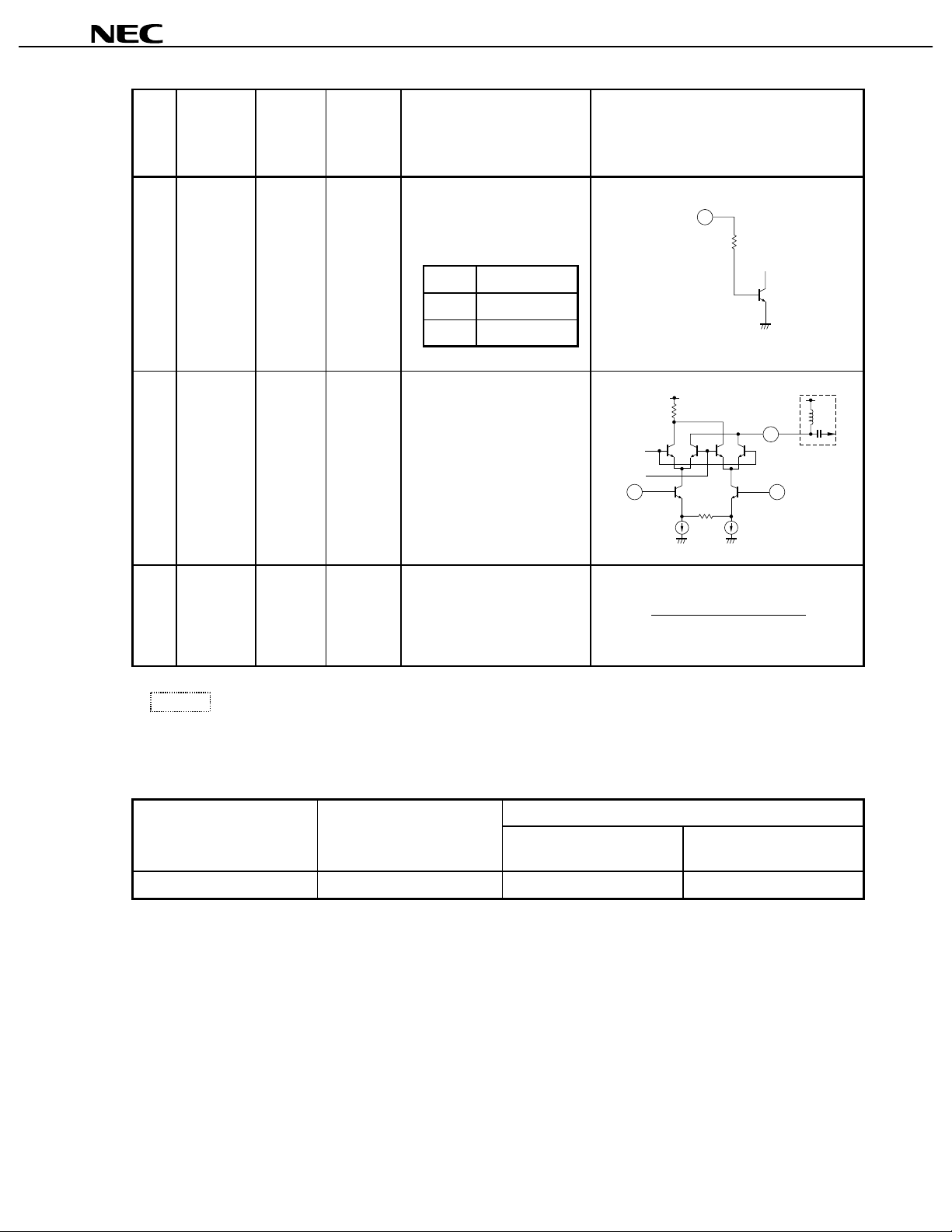
µµµµ
16
1.6 k
2 3
19
PC8125GR
Pin
NO.
Symbol
16 V
19 RF
Supply
Voltage
(V)
PS
0 to V
Voltage
Function and Description Internal Equivalent Circuit
Typ. (V)
CC
= 3 V
@V
CC
−
Power save control pin for
phase shifter and up-converter
can controlled the On/Sleep
state with bias as follows:
Pin
VPS(V) STATE
2 to VCCON (Active Mode)
0 to 0.5 OFF (Sleep Mode)
out
CC
V
−
RF output from up-converter.
This pin is open collect or
output and should be matched
external circuit.
20 V
(Up-con.)
CC
2.7 to
5.5
−
Supply voltage pin for the
up-converter.
An internal regulator helps
keep the device stable against
CC
temperature or V
variation.
: Externally
6. RELATIONS BETWEEN AMPLITUDE AND VCC/2 BIAS OF I/Q INPUT SIGNALS
Supply voltage
CC
V
(V)
I/Q DC Voltage(V)
CC
V
/2 = I = Ib = Q = Qb
2.7 to 3.0 to 5.5 1.35 to 1.5 to 2.75
Single ended input
I/Q Input signal (mVp-p)
I = Q
500
≤
Differential input
I = Ib = Q = Qb
≤
250
Data Sheet P11486EJ2V0DS00
9
 Loading...