

DATA SHEET
BIPOLAR ANALOG INTEGRATED CI RCUIT
PC8105GR
µµµµ
400 MHz QUADRATURE MODULATOR
FOR DIGITAL MOBILE COMMUNICATION
DESCRIPTION
The µPC8105GR is a sillicon monolithic integrated circuit designed as quadrature modulator for digital mobile
communication systems. This modulator housed in a 16 pin plastic SSOP that is easy to install and contributes to
miniaturizing the system.
The device has power save function and can operates 2.7 to 5.5 V supply voltage to realize low power
consumption.
FEATURES
•
Internal 90° phase shifter is accurate over an IF range from 100 MHz to 400 MHz.
•
Wide supply voltage range: VCC = 2.7 to 5.5 V.
•
Low operation current: ICC = 16 mA (typ.).
•
16 pin plastic SSOP suitable for high density surface mounting.
•
Low current in sleep mode
APPLICATION
•
IF modulator for Digital cellular phone (PDC, IS-54, GSM etc..)
•
IF modulator for Digital cordless phone (PHS, PCS etc..)
ORDERING INFORMATION
PART NUMBER PACKAGE SUPPLYING FORM
µ
PC8105GR-E1 16 pin plastic SSOP (225 m i l ) Carrier tape width 12 mm. Q’ty 2. 5 kp/Reel
Pin 1 indicated pull-out direc tion of tape.
To order evaluation samples, please contact your local NEC sales office. (Part number for sample order:
PC8105GR)
µ
The information in this document is subject to change without notice. Before using this document, please
confirm that this is the latest version.
Not all devices/types available in every country. Please check with local NEC representative for
availability and additional information.
Document No. P10807EJ3V0DS00 (3rd edition)
Date Published October 1999 N CP(K)
Printed in Japan
Caution electro-static sensitive device
The mark shows major revised points.
©
1995, 1999
SERIES PRODUCTS
µµµµ
PC8105GR
SERIES TYPE
150 MHz Quadrature MOD
Up-Con + Quadrature MOD
400 MHz Quadrature MOD
Remark:
As for detail information of series products, please refer to each data sheet.
PART
NUMBER
PC8101GR 100 to
µ
PC8104GR 100 to 400 DC to 10 800 to 1900 Digital Comm.
µ
PC8105GR 100 to 400 DC to 10 External Digital Comm.
µ
f LO1 in
(MHz)
300
f MODout
(MHz)
50 to 150 DC to 0.5 External CT2, Digital Comm.
f I/Q
(MHz)
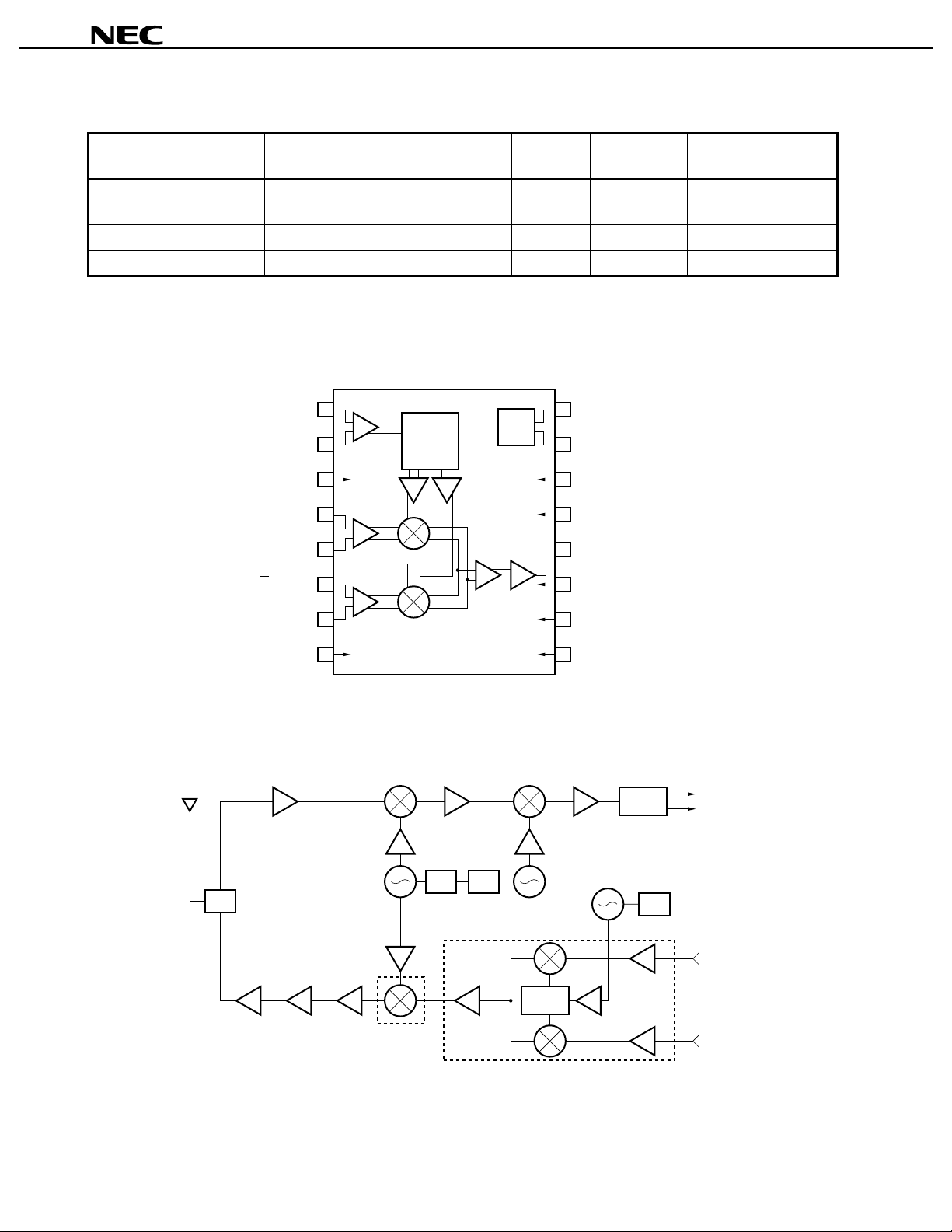
INTERNAL BLOCK DIAGRAM AND PIN CONNECTIONS (Top View)
LO
LO
GND
I-INPUT
I-INPUT
Q-INPUT
1
in
90˚
in
2
3
4
5
6
Phase
Sifter
REG.
V
16
CC
15
Power Save
14
GND
13
GND
12
MOD
11
N.C.
Up-Converter
f RFout (MHz)
out
APPLICATIONS
Q-INPUT
GND
APPLICATION EXAMPLE
[Digital cellular hand-held phone]
Low-noise transistor
RX
SW
TX
PA
10
7
8
÷N
VCO
PLL
µ
Phase
shifter
µ
PC8106T
N.C.
9
N.C.
PC8105GR
0˚
90˚
DEMO
PLL
I
Q
I
Q
2
Data Sheet P10807EJ3V0DS00
ABSOLUTE MAXIMUM RATINGS
PARAMETER SYMBOL RATING UNIT TEST CONDITIONS
µµµµ
PC8105GR
Supply Voltage V
Power Save Voltage V
Power Dissipation P
Operating Temperature T
Storage Temperature T
: Mounted on 50 × 50 × 1.6 mm double copper clad epoxy glass board
*1
CC
PS
D
op
stg
6.0 V TA = +25 °C
6.0 V TA = +25 °C
310 mW
40 to +85
−
55 to +150
−
RECOMMENDED OPERATING CONDITIONS
PARAMETER SYMBOL MIN. TYP. MAX. UNIT TEST CONDITIONS
Supply Voltage V
Operating Temperature T
Modulator Output Frequency f
LO1 Input Frequency f
I/Q Input Frequency f
ELECTRICAL CHARACTERISTICS (TA = +25
CC
A
MODout
LO1in
I/Qin
2.7 3.0 5.5 V
40 +25 +85
−
100 400 MHz
DC 10 MHz P
C, VCC = 3.0 V, Unless Otherwise Specified VPS
°°°°
A
T
= +85 °C
C
°
C
°
C
°
LOin
P
= −10 dBm
I/Qin
= 600 mV
*1
p-p
MAX (Single ended)
1.8 V)
≥≥≥≥
PARAMETER SYMBOL MIN. TYP. MAX. UNIT TEST CONDITIONS
Circuit Current I
Circuit Current at Power
CC
10 16 21 m A No input signal
ICC(PS) 0.1 5
AVPS ≤ 1.0 V
µ
Save Mode
Output Power P
LO Carrier Leak LOL
Image Rejection
MODout
ImR
−
21.0
−
16.5
40
−
40
−
12.0 dBm
−
30 dBc
−
30 dBc
−
I/Q DC = 1.5 V
I/Qin
= 500 mV
P
(Side Band Leak)
p-p
(Single ended)
Data Sheet P10807EJ3V0DS00
3
STANDARD CHARACTERISTICS FOR REFERENCE
(TA = +25
C, VCC = 3.0 V, Unless Otherwise Specified VPS
°°°°
PARAMETER SYMBOL MIN. TYP. MAX. UNIT TEST CONDITIONS
1.8 V)
≥≥≥≥
µµµµ
PC8105GR
I/Q 3rd Order
IM
Intermodulation Distort i on
I/Q Input Impedance Z
I/Q Bias Current I
LO1 Input VSWR Z
Power Save Rise Time T
Power Save Fall Time T
3I/Q
I/Q
I/Q
LO
PS(RISE)
PS(FALL)
50
−
30 dBc I/Q DC = 1.5 V
−
20 k
5
1.2:1
25
25
Ω
A
µ
I/Qin
= 500 mV
P
I/Q DC = 1.5 V
I/Qin
= 500 mV
P
(I → I, Q → Q)
p-p
p-p
−
sVPS(OFF) → VPS(ON)
µ
sVPS(ON) → VPS(OFF)
µ
(Single ended)
(Single ended)
4
Data Sheet P10807EJ3V0DS00
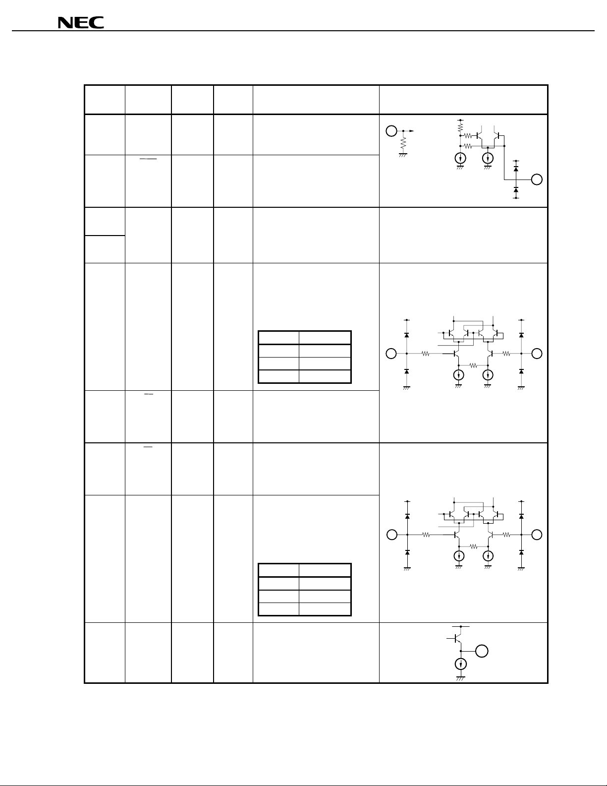
PIN EXPLANATION
µµµµ
PC8105GR
PIN NO.
ASSIGNMENT
1LOin
2LOin
SUPPLY
VOL. (V)
−
−
3GND0
8
4IV
CC
PIN
VOL.(V)
FUNCTION AND APPLICATION EQUIPMENT CIRCUIT
0 LO input for phase shifter.
This input impedance is 50
matched internally.
Ω
1
50 Ω
2.4 Bypass of LO input.
This pin is grounded through
2
internal capacitor.
Open in case of single ended.
−
Connect to the ground with
minimum inductance.
Track length should be kept as
short as possible.
/2
Input for I signal. This in put
−
impedance is larger than 20 kΩ.
Relations between amplitude and
CC
/2 bias of input signal are
V
following.
VCC/2 (v) Amp. (mV
1.35 400
≥
1.5 600
≥
1.75 1000
≥
p-p
)
*1
4 5
5IV
6QV
7QV
12 MODout
CC
/2
CC
/2
CC
/2
−
Input for I signal. This in put
−
impedance is larger than 20 kΩ.
CC
/2 biased DC signal should be
V
input.
Input for Q signal. This i n put
−
impedance is larger than 20 kΩ.
CC
/2 biased DC signal should be
V
input.
Input for Q signal. This i n put
−
impedance is larger than 20 kΩ.
Relations between amplitude and
CC
/2 bias of input signal are
V
following.
VCC/2 (v) Amp. (mV
1.35 400
≥
1.5 600
≥
1.75 1000
≥
1.5 Output from modulator.
This is emitter follower output.
7 6
p-p
)
*1
12
In case of that I/Q input signals are single ended.
*1:
Of course, I/Q signal inputs can be used either single endedly or differentially with proper terminations.
Data Sheet P10807EJ3V0DS00
5

×2
from LO
in
÷2 F/F
I
I
Q
Q
to MOD
out
PIN EXPLANATION
15
µµµµ
PC8105GR
PIN NO.
13 GND 0
14
15 Power
16 V
ASSIGNMENT
Save
SUPPLY
VOL. (V)
VP/S
CC
2.7 to
5.5
PIN
VOL.(V)
−
−
−
FUNCTION AND APPLICATION EQUIPMENT CIRCUIT
Connect to the ground with
minimum inductance.
Track length should be kept as
short as possible.
Power save control pin can be
controlled ON/SLEEP state with
bias as follows;
VP/S (v) STATE
1.8 to 5.5 ON
0 to 1.0 SLEEP
Supply voltage pin for modulator.
Internal regulator can be kept
stable condition of suppl y bias
against the variable temperat ure
CC
.
or V
EXPLANATION OF INTERNAL FUNCTION
BLOCK FUNCTION/OPERATI ON BLOCK DIAGRAM
90° PHASE
SHIFTER
BUFFER AMP. Buff er am pl i f i ers for each phase signals to
MIXER Each signals from buffer amp. are
ADDER Output signals from each mixers are added
Input signal from LO is s end to digital
circuit of T-type f l i p-flop through frequency
doubler. Output signal from T-ty pe F/ F i s
changed to same frequency as LO i nput
and that have quadrature phase shift, 0°,
90°, 180°, 270°. These circuits hav e
function of self phas e correction to make
correctly quadrature signals.
send to each mixers.
quadrature modulated with two doublebalanced mixers.
High accurate phase and amplitude i nput s
are realized to good performance for im age
rejection.
with adder and send to final amplif i er.
6
Data Sheet P10807EJ3V0DS00

µµµµ
PC8105GR
TYPICAL CHARACTERISTICS (TA = +25
CC
Unless otherwise specified V
(single ended), P
LOin
= −10 dBm, (continuous wave)
= VPS = 3 V, I/Q DC offset = I/Q DC offset = 1.5 V, I/Q Input Signal = 500 mV
SUPPLY VOLTAGE vs CIRCUIT CURRENT
40
35
30
25
20
- Circuit Current - mA
15
CC
I
C)
°°°°
p-p
Lo INPUT POWER vs OUTPUT POWER,
LOCAL LEAK, IMAGE REJECTION,
I/Q 3RD ORDER INTERMODULATION
DISTORTION
10
0
I/Q - dBc
3
–10
–20
–30
–40
(PHS)
384 Kbps
RNYQ
α = 0.5
(0000)
All zero
Pout
LOL(ISO(LO))
ImR
–10
–20
–30
- Modulator Output Power - dBm
10
5
0
0123456
CC
- Supply Voltage - V
V
VCC = VPS = 3 V
RF None
) - Local Leak, ImR - Image Rejection, IM
–50
LO
LOL (ISO
–60
–70
–30 –20 –10 0 +10
P
Loin
- Lo Input Power - dBm
IM
3I/Q
–40
–50
MODout
P
Data Sheet P10807EJ3V0DS00
7

µµµµ
PC8105GR
I/Q INPUT SIGNAL vs OUTPUT POWER,
LOCAL LEAK, IMAGE REJECTION,
I/Q 3RD ORDER INTERMODULATION
DISTORTION
10
(PHS)384 Kbps
RNYQ α = 0.5
(0000) All zero
0
–10
–20
–30
–40
–50
LOL (ISOLO) - Local Leak, ImR - Image Rejection, IM3 I/Q - dBc
–60
ImR
Pout
LOL(ISO(LO))
IM3I/Q
Lo INPUT FREQUENCY vs OUTPUT POWER,
LOCAL LEAK, IMAGE REJECTION, I/Q 3RD,
ORDER INTERMODULATION DISTORTION
–10
–20
–30
PMODout - Modulator Output Power - dBm
–40
–10
–20
–30
–40
–50
–60
LOL(ISOLO) - Local Leak, ImR - Image Rejection, IM3 I/Q - dBC
–70
P
out
ImR
LOL(ISO(LO))
IM
3I/Q
50 100 200 500
fLO - Lo Input Frequency - MHz
–10
–20
–30
–40
–50
MODout - Modulator Output - Power - dBm
P
–60
–70
–70
0 0.5 1
P
I/Qin - I/Q Input Signal - Vp-p
I/Q INPUT SIGNAL vs PHASE ERROR,
MAGNITUDE ERROR, VECTOR ERROR
VCC = 3 V
Lo: 240 MHz
10
–10 dBm
I/Q DC: 1.5 V
Single ended
<PHS>
384 Kbps
7
RNYQ α = 0.5
PN9
5
φ
∆ - Phase Error - deg.
∆A - Magnitude Error - % rms
∆M - Vector Error - % rms
3
2
1
0
0 0.5 1
I/Qin - I/Q Input signal - mVp-p
P
∆M
∆A
∆
–50
Lo INPUT FREQUENCY vs VECTOR ERROR,
MAGNITUDE ERROR, PHASE ERROR
VCC = 3 V
Lo: 15 dBm
I/Q DC 1 500 mV
10
AC 430 mV
<PHS>384 Kbps
RNYQ α = 0.5
PN9
7
5
φ
∆ - Phase Error - deg.
∆A - Magnitude Error - % rms
∆M - Vector Error - % rms
φ
3
2
1
0
0 200 400
p-p
∆M
∆A
φ
∆
100 300 500
LO - Lo Input Frequency - MHz
f
8
Data Sheet P10807EJ3V0DS00

TYPICAL SINE WAVE MODULATION
OUTPUT SPECTRUM
µµµµ
PC8105GR
10 dB/
RBW
1 kHz
VBW
1 kHz
SWP
2.0 s
ATT 10 dBREF 0.0 dBm
CENTER 240.0000 MHz
<PHS>384 kbps, RNYQ α = 0.5, MOD Pattern<000>, all zero
SPAN 200.0 kHz
TYPICAL π/4 DQPSK MODULATION OUTPUT SPECTRUM
<PHS>384 kbps, RNYQ α = 0.5, MOD Pattern (PN9)
TYPICAL π/4 DQPSK MODULATION OUTPUT SPECTRUM
<PDC>42 kbps, RNYQ α = 0.5, MOD Pattern<PN9>
REF –10.0 dBm
10 dB/
ADJ BS
192 kHz
DL –10.0 dBm
RBW 3 kHz
VBW 10 kHz
SWP 5.0 s
1
CENTER 240.000 MHz SPAN 2.000 MHz
ATT 0 dB
MARKER
239.100 MHz
68.75 dB
2
∗∗∗ Multi Marker List ∗∗∗
No.1: 239.100 MHz –68.75 dB
No.2: 239.400 MHz –68.25 dB
No.3: 240.600 MHz –68.25 dB
No.4: 240.900 MHz –69.00 dB
3
REF –10.0 dBm
10 dB/
ADJ BS
21.0 kHz
4
DL –10.0 dBm
RBW 3 kHz
VBW 3 kHz
SWP 5.0 s
CENTER 240.0000 MHz SPAN 500 kHz
ATT 0 dB
MARKER
289.9000 MHz
76.50 dB
23
1
∗∗∗ Multi Marker List ∗∗∗
No.1: 239.9000 MHz –76.50 dB
No.2: 239.9500 MHz –70.50 dB
No.3: 240.0500 MHz –71.00 dB
No.4: 240.1000 MHz –75.75 dB
4
Data Sheet P10807EJ3V0DS00
9
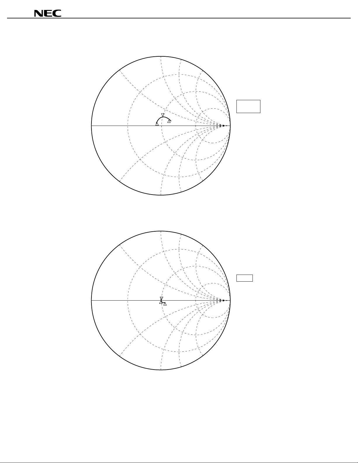
MODout OUTPUT IMPEDANCE
MARKER 2
240 MHz
2; 49.244 Ω 13.58 Ω 9.0056 nH
240.000 000 MHz
µµµµ
PC8105GR
LOin INPUT IMPEDANCE
MARKER 2
240 MHz
2
3
1
STOP 500.000 000 MHzSTART 50.000 000 MHz
2; 51.727 Ω –2.0059 Ω 330.5 pF
240.000 000 MHz
MOD out
Marker
1. 100 MHz
2. 240 MHz
3. 400 MHz
10
2
3
1
STOP 500.000 000 MHzSTART 50.000 000 MHz
Data Sheet P10807EJ3V0DS00
Lo in
Marker
1. 100 MHz
2. 240 MHz
3. 400 MHz

TEST CIRCUIT
fMOD out = 100 ~ 400 MHz
S.P.A
µµµµ
PC8105GR
V
CC
LO
S.G
f
LO
= 100 ~ 400 MHz
IN
= –10 dBm
P
GND
I
1 000 pF
MOD out
I
p-p
(I, Q only)
NC
Q
10 kΩ
16 15 14 13 12 11 10 9
CC
V
Lo in
12345678
Open
1 000 pF
GND
Power Save
Lo in
GND
IIQQ
I/Q Signal Generator
f : DC to hundreds kHz
A : 0.5 V
V : 1.5 V (I, I, Q, Q)
NC
Q
NC
GND
Data Sheet P10807EJ3V0DS00
11
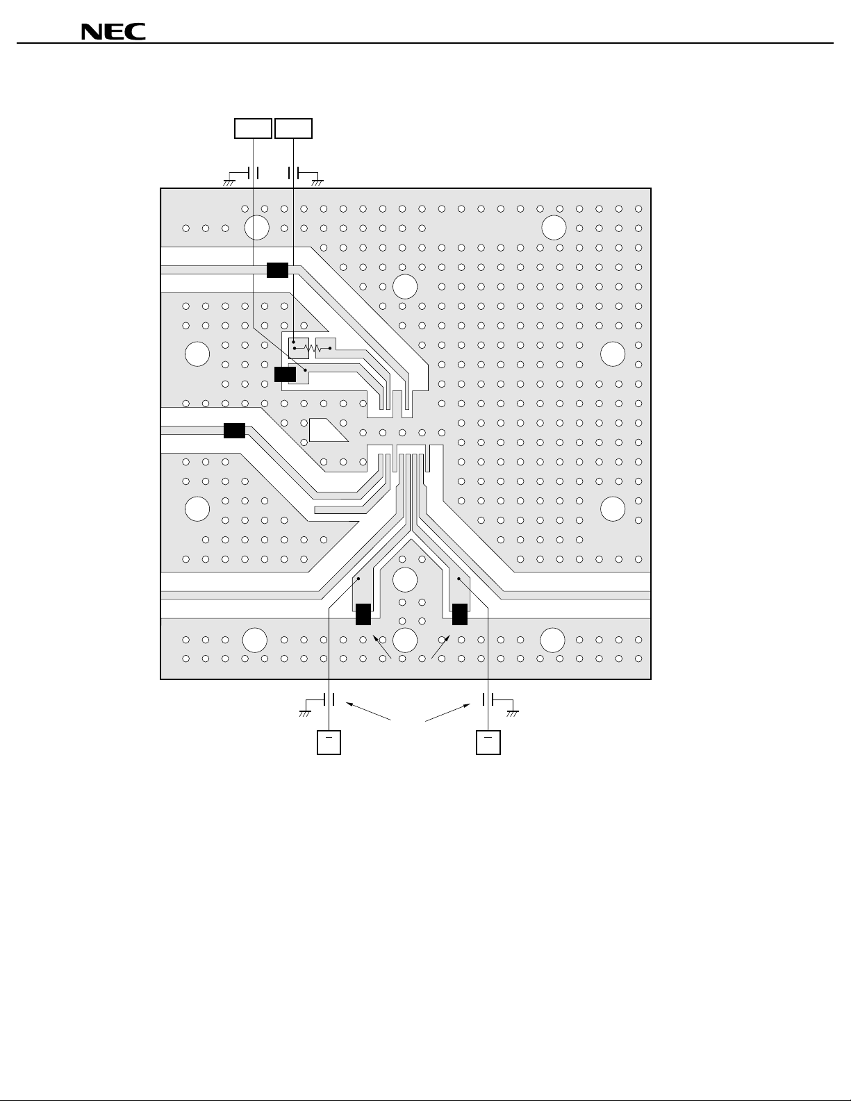
TEST BOARD
I F OUT
CC
1 000 pF
µµµµ
PC8105GR
P. S.V
10 000 pF10 000 pF
µ
PC8105GR
10 kΩ
LO IN
1 000 pF
1
1 000 pF
I IN Q IN
10 000 pF
IQ
10 000 pF
12
Data Sheet P10807EJ3V0DS00

PACKAGE DIMENSIONS
16 PIN PLASTIC SHRINK SOP (225 mil) (UNIT: mm)
16 9
detail of lead end
5° ± 5°
µµµµ
PC8105GR
18
1.565 ± 0.235
1.44
0.125 ± 0.075
NOTE Each lead centerline is located within 0.10 mm of its true position (T.P.) at maximum material condition.
5.2 ± 0.3
0.65
0.22 ± 0.08
0.475 MAX.
M
0.10
6.2 ± 0.3
4.4 ± 0.2
S
0.5 ± 0.2
+0.08
0.17
−0.07
0.9 ± 0.2
0.10
S
Data Sheet P10807EJ3V0DS00
13
µµµµ
PC8105GR
NOTE ON CORRECT USE
(1) Observe precautions for handling because of electrostatic sensitive devices.
(2) Form a ground pattern as widely as possible to minimize ground impedance (to prevent undesired oscillation).
(3) Keep the track length of the ground pins as short as possible.
CC
(4) Connect a bypass capacitor (e.g. 1 000 pF) to the V
pin.
(5) I, Q DC offset voltage should be same as the I, Q DC offset voltage (to prevent changing the local leak level with
power save control.)
RECOMMENDED SOLDERING CONDITIONS
This product should be soldered in the following recommended conditions. Other soldering methods and
conditions than the recommended conditions are to be consulted with our sales representatives.
PC8105GR
µµµµ
Soldering process Soldering Conditions Symbol
Infrared ray reflow Peak package’s surface temperature: 235 °C or below,
Reflow time: 30 seconds or bel ow (210 °C or higher),
Number of reflow process: 3, Exposure limit
VPS Peak package’s surface temperature: 215 °C or below,
Reflow time: 30 seconds or bel ow (200 °C or higher),
Number of reflow process: 3, Exposure limit
Wave soldering Solder temperature: 260 °C or below
Flow time: 10 seconds or below,
Number of reflow process: 1, Exposure limit
Partial heating method Terminal temperature: 300 °C or below
Flow time: 3 seconds/pi n or bel ow,
Exposure limit
Exposure limit before soldering after dry-pack package is opened.
*:
*
: None
*
: None
*
: None
*
: None
IR35-00-3
VP15-00-3
WS60-00-1
Storage conditions: 25 °C and relative humidity at 65 % or less.
Apply only a single process at once, except for “Partial heating method”.
Note:
For details of recommended soldering conditions for surface mounting, refer to information document
SEMICONDUCTOR DEVICE MOUNTING TECHNOLOGY MANUAL (C10535E).
The application circuits and their parameters are for reference only and are not intended for use in actual design-ins.
14
Data Sheet P10807EJ3V0DS00

[MEMO]
µµµµ
PC8105GR
Data Sheet P10807EJ3V0DS00
15

µµµµ
PC8105GR
• The information in this document is subject to change without notice. Before using this document, please
confirm that this is the latest version.
• No part of this document may be copied or reproduced in any form or by any means without the prior written
consent of NEC Corporation. NEC Corporation assumes no responsibility for any errors which may appear in
this document.
• NEC Corporation does not assume any liability for infringement of patents, copyrights or other intellectual property
rights of third parties by or arising from use of a device described herein or any other liability arising from use
of such device. No license, either express, implied or otherwise, is granted under any patents, copyrights or other
intellectual property rights of NEC Corporation or others.
• Descriptions of circuits, software, and other related information in this document are provided for illustrative
purposes in semiconductor product operation and application examples. The incorporation of these circuits,
software, and information in the design of the customer's equipment shall be done under the full responsibility
of the customer. NEC Corporation assumes no responsibility for any losses incurred by the customer or third
parties arising from the use of these circuits, software, and information.
• While NEC Corporation has been making continuous effort to enhance the reliability of its semiconductor devices,
the possibility of defects cannot be eliminated entirely. To minimize risks of damage or injury to persons or
property arising from a defect in an NEC semiconductor device, customers must incorporate sufficient safety
measures in its design, such as redundancy, fire-containment, and anti-failure features.
• NEC devices are classified into the following three quality grades:
"Standard", "Special", and "Specific". The Specific quality grade applies only to devices developed based on a
customer designated "quality assurance program" for a specific application. The recommended applications of
a device depend on its quality grade, as indicated below. Customers must check the quality grade of each device
before using it in a particular application.
Standard: Computers, office equipment, communications equipment, test and measurement equipment,
audio and visual equipment, home electronic appliances, machine tools, personal electronic
equipment and industrial robots
Special: Transportation equipment (automobiles, trains, ships, etc.), traffic control systems, anti-disaster
systems, anti-crime systems, safety equipment and medical equipment (not specifically designed
for life support)
Specific: Aircraft, aerospace equipment, submersible repeaters, nuclear reactor control systems, life
support systems or medical equipment for life support, etc.
The quality grade of NEC devices is "Standard" unless otherwise specified in NEC's Data Sheets or Data Books.
If customers intend to use NEC devices for applications other than those specified for Standard quality grade,
they should contact an NEC sales representative in advance.
M7 98. 8
 Loading...