NEC UPC8104GR-E1, UPC8104GR Datasheet

DATA SHEET
DATA SHEET
BIPOLAR ANALOG INTEGRATED CI RCUIT
PC8104GR
µµµµ
UP CONVERTER + QUADRATURE MODULATOR IC
FOR DIGITAL MOBILE COMMUNICATION SYSTEMS
DESCRIPTION
The µPC8104GR is a silicon monolithic integrated circuit designed as quadrature modulator for digital mobile
communication systems. This modulator consists of 1.9 GHz up-converter and 400 MHz quadrature modulator which
are packaged in 20 pin SSOP. The device has power save function and can operate 2.7 to 5.5 V supply voltage,
therefore, it can contribute to make RF block small, high performance and low power consumption.
FEATURES
•
20 pin SSOP suitable for high density surface mounting.
•
High linearity up converter is incorporated; P
•
Low phase difference due to digital phase shifter is adopted.
•
Wide operating frequency range. Up converter; f
Modulator ; f
•
External IF filter can be applied between modulator output and up converter input terminal.
•
Supply voltage: VCC = 2.7 to 5.5 V
•
Equipped with power save function.
RFout(sat)
RFout
MODout
= −6 dBm TYP.
= 800 MHz to 1.9 GHz
= 100 MHz to 400 MHz, f
I/Q
= DC to 10 MHz
APPLICATION
•
Digital cordless phones
•
Digital cellular phones
ORDERING INFORMATION
PART NUMBER PACKAGE SUPPLYING FORM
µ
PC8104GR-E1 20 pin plastic SSOP Embossed tape 12 mm wide. QTY 2.5 kp/Reel.
Pin 1 indicates pull-out di rection of tape.
* For evaluation sample order, please contact your local NEC sales office. (Order number: µPC8104GR)
Caution electro-static sensitive device
The information in this document is subject to change without notice. Before using this document, please
confirm that this is the latest version.
Not all devices/types available in every country. Please check with local NEC representative for
availability and additional information.
Document No. P10099EJ4V0DS00 (4th edition)
Date Published October 1999 N CP(K)
Printed in Japan
The mark shows major revised points.
©
1995, 1999
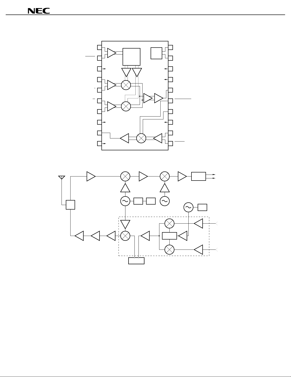
INTERNAL BLOCK DIAGRAM AND PIN CONNECTIONS (Top View)
1
Lo1 in
Lo1 in
GND
(MOD)
90˚
2
3
4
I
Phase
Shifter
REG.
CC
20
V
Power Save
19
GND
18
GND
17
µµµµ
PC8104GR
APPLICATION EXAMPLE
(PHS)
RX
SW
TX
PA
Q
Q
GND
(UP Con)
RF out
GND
(UP Con)
5
I
6
7
8
9
10
PLL÷N
PC8104GR
µ
MOD out
16
Up Con in
15
Up Con in
14
V
13
(UP Con)
Lo2 in
12
Lo2 in
11
0˚
φ
90˚
CC
DEMO.
PLL
I
Q
I
Q
Filter
2
Data Sheet P10099EJ4V0DS00
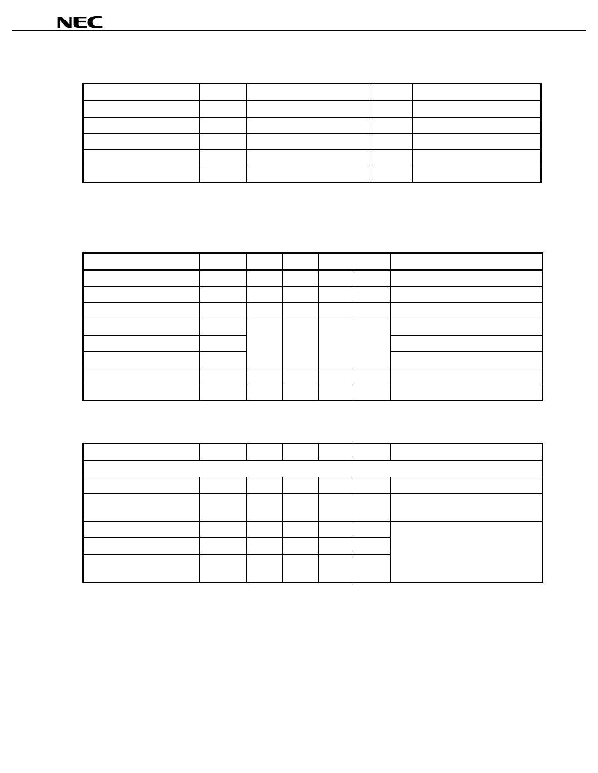
ABSOLUTE MAXIMUM RATINGS
PARAMETER SYMBOL RATING UNIT TEST CONDITION
µµµµ
PC8104GR
Supply Voltage V
Power Save Voltage V
Power Dissipation P
Operating Temperature T
Storage Temperature T
: Mounted on 50 × 50 × 1.6 mm double copper clad epoxy glass board
Note 1
CC
PS
D
A
stg
RECOMMENDED OPERATING CONDITIONS
PARAMETER SYMBOL MIN. TYP. MAX. UNIT TEST CONDITIONS
Supply Voltage V
Operating Temperature T
Up Converter RF Frequency f
Up Converter Input Freq. f
Modulator Output Frequency f
Lo1 Input Frequency f
Lo2 Input Frequency f
I/Q Input Frequency f
CC
A
RFout
UpConin
MODout
Lo1in
Lo2in
I/Qin
2.7 3.0 5.5 V
40 +25 +85
−
0.8 1.9 GHz
100 400 MHz
800 1800 MHz P
DC 10 MHz P
6.0 V TA = +25 °C
6.0 V TA = +25 °C
C
C
P
T
Lo1in
= −10 dBm
Lo2in
= −10 dBm
I/Qin
= 600 mV
430 mW
40 to +85
−
55 to +150
−
°
°
C
°
A
= +85 °C
Note1
p-p
MAX (Single ended)
ELECTRICAL CHARACTERISTICS (TA = +25
PARAMETER SYMBOL MIN. TYP. MAX. UNIT TEST CONDITIONS
UP CONVERTER + QUADRATURE MODULATOR TOTAL
Total Circuit Current I
Total Circuit Current at
Power-Save Mode
Total Output Power P
Lo Carrier Leak
Note2
Image Rejection (Side Band
Leak)
: Lo1 + Lo2
Note 2
ccTOTAL
cc(PS)TOTAL
I
RFout
LOL
ImR
18 28 37 m A No input signal
18.5
−
C, VCC = 3.0 V, Unless Otherwise Specified VPS
°°°°
0.1 10
13.5
−
40
−
40
−
8.5 dBm
−
30 dBc
−
30 dBc
−
AVPS ≤ 1.0 V
µ
I/Q DC = 1.5 V
I/Qin
= 500 mV
P
p-p
(Single ended)
1.8 V)
≥≥≥≥
Data Sheet P10099EJ4V0DS00
3
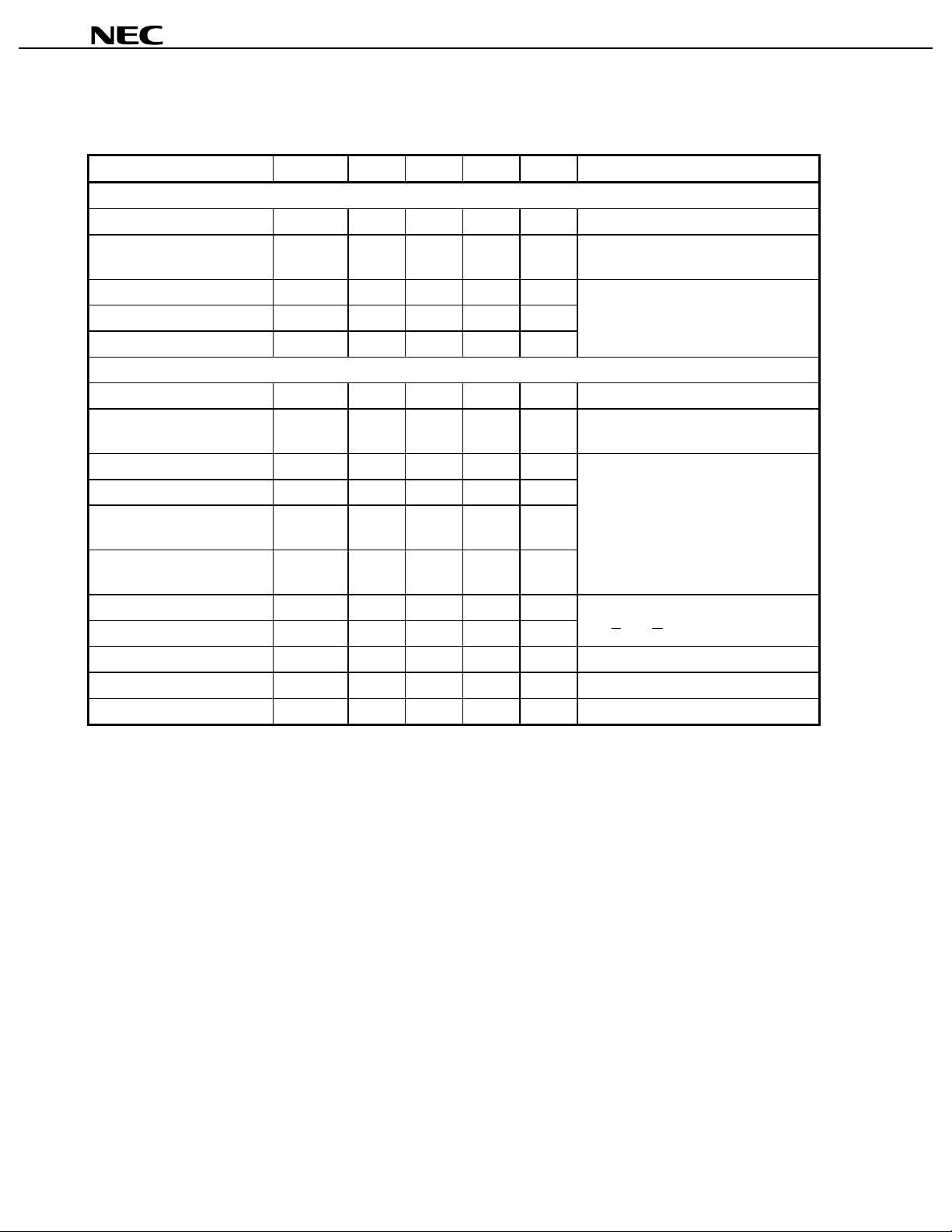
STANDARD CHARACTERISTICS FOR REFERENCE
(TA = +25
UP CONVERTER BLOCK
Up Con. Circuit Current I
Up Con. Circuit Current at
Power-Save Mode
Conversion Gain CG 4 dB f
Maximum Output Power P
Output Intercept Point OIP3 0 dBm
QUADRATURE MODULATOR BLOCK
MOD. Circuit Current I
MOD. Circuit Current at
Power-Save Mode
Output Power P
Lo1 Carrier Leak LOL
Image Rejection
(Side Band Leak)
I/Q 3rd Order Intermodulation
Distortion
I/Q Input Impedance Z
I/Q Bias Current I
Lo1 Input VSWR Z
Power Save Rise Time T
Power Save Fall Time T
C, VCC = 3.0 V, Unless Otherwise Specified VPS
°°°°
1.8 V)
≥≥≥≥
PARAMETER SYMBOL MIN. TYP. MAX. UNIT TEST CONDITIONS
ccUpCon
cc(PS)UpCon
I
RF(sat)
ccMOD
cc(PS)MOD
I
MODout
ImR
M3I/Q
I
I/Q
I/Q
Lo1
PS(RISE)
PS(FALL)
10 16 21 m A No input signal
12 m A No input signal
5
6dBm
−
5
16.5 dBm
−
40
−
40
−
50
−
30 dBc
−
30 dBc
−
30 dBc
−
20 k
5
AVPS ≤ 1.0 V
µ
AVPS ≤ 1.0 V
µ
Ω
A
µ
1.2:1 X:1
2.0 5.0
2.0 5.0
sV
µ
sV
µ
RFout
= 1.9 GHz
UpConin
= 240.0 MHz/240.2 MHz
f
I/Q DC = 1.5 V
I/Qin
P
= 500 mV
p-p
I/Q DC = 1.5 V
I/Qin
P
= 500 mV
p-p
(I → I, Q → Q)
PS(OFF)
PS(ON)
→ V
→ V
PS(ON)
PS(OFF)
µµµµ
PC8104GR
(Single ended)
(Single ended)
4
Data Sheet P10099EJ4V0DS00
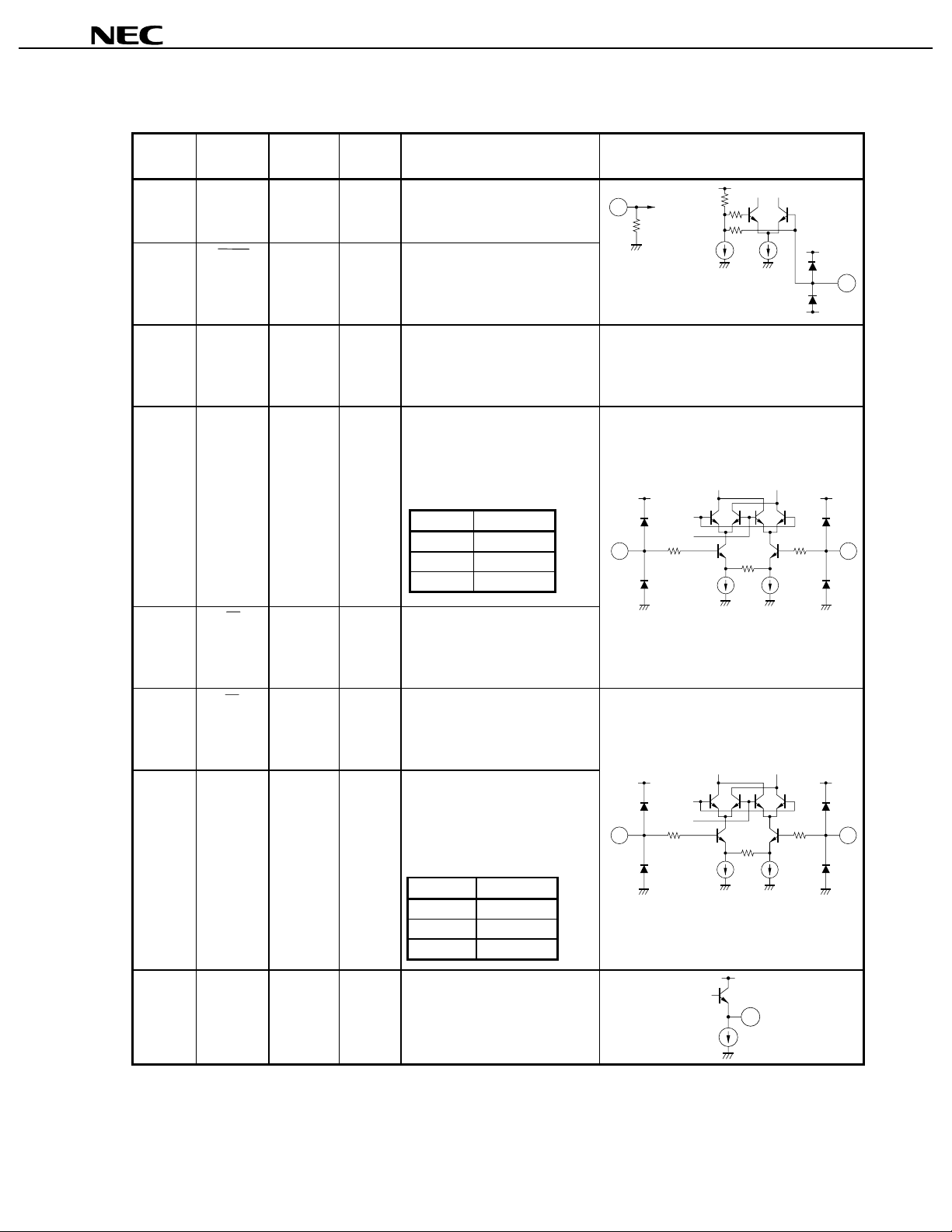
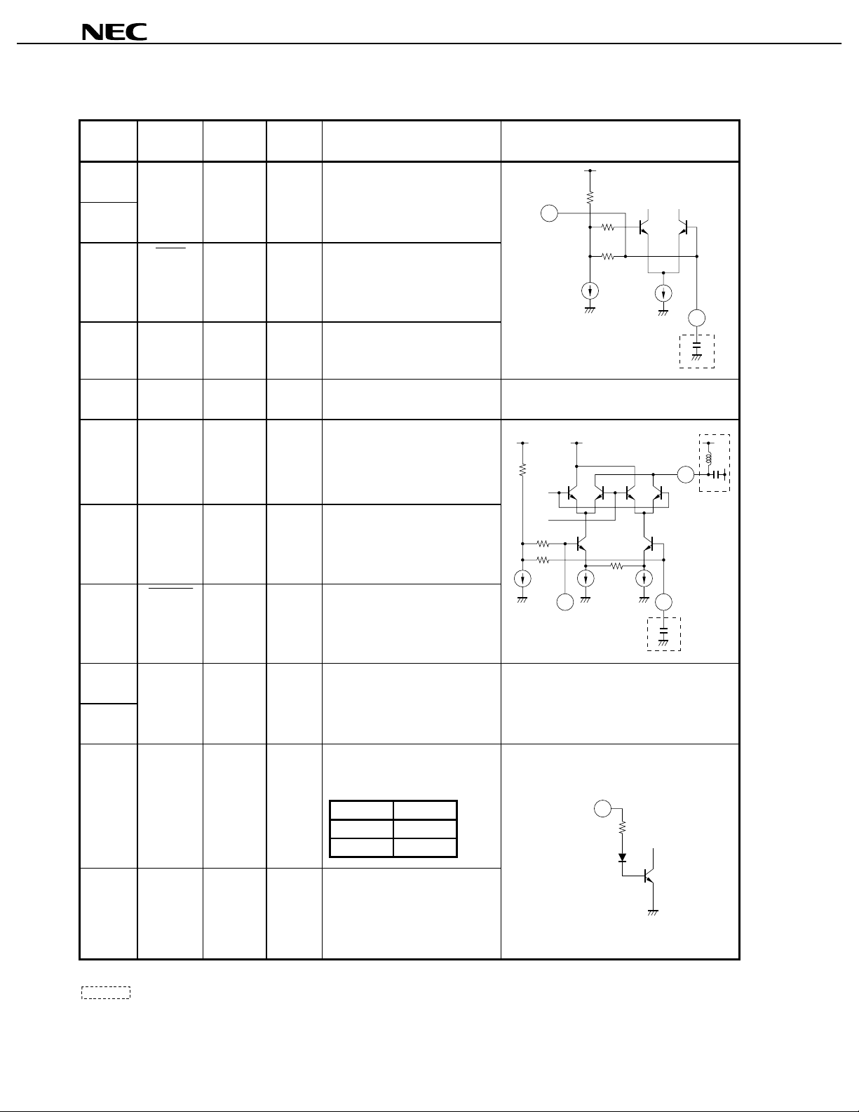
PIN EXPLANATION
µµµµ
PC8104GR
PIN
NO.
ASSIGNMENT
1 Lo1in
2 Lo1in
3 G ND for
SUPPLY
VOL. (V)
−
−
0
modulator
4IV
CC
/2
PIN
VOL.(V)
FUNCTION AND APPLICATION EQUIPMENT CIRCUIT
0 Lo1 input for phase shi f ter.
This input impedance is 50
matched internally.
2.4 Bypas s of Lo1 input.
This pin is grounded through
internal capacitor.
Open in case of single ended.
Connect to the ground with
−
minimum inductance.
Track length should be kept as
short as possible.
Input for I signal. This input
−
impedance is larger than 20 kΩ.
Relations between amplitude
CC
/2 bias of input signal
and V
are following.
VCC/2 (v) Amp. (mV
1.35 400
≥
1.5 600
≥
1.75 1000
≥
Ω
p-p
)
Note
1
50 Ω
2
45
5IV
6QV
7QV
16 MODout
CC
/2
CC
/2
CC
/2
−
Input for I signal. This input
−
impedance is larger than 20 kΩ.
CC
/2 biased DC signal should
V
be input.
Input for Q signal. This i nput
−
impedance is larger than 20 kΩ.
CC
/2 biased DC signal should
V
be input.
Input for Q signal. This i nput
−
impedance is larger than 20 kΩ.
Relations between amplitude
CC
/2 bias of input signal
and V
are following.
VCC/2 (v) Amp. (mV
1.35 400
≥
1.5 600
≥
1.75 1000
≥
1.5 Output from modulator.
This is emitter follower output.
76
p-p
)
Note
16
In case of that I/Q input signals are single ended.
Note
Of course, I/Q signal inputs can be used either single endedly or differentially with proper terminations.
Data Sheet P10099EJ4V0DS00
5
PIN EXPLANATION
µµµµ
PC8104GR
PIN
NO.
10
11 Lo2in
12 Lo2in
13 VCC for Up-
14 UpConin
ASSIGNMENT
GND
80
for Upconverter
converter
9 RFout V
SUPPLY
VOL. (V)
−
−
2.7 to 5.5
CC
−
PIN
VOL.(V)
2.0 Bypas s of Lo2 input.
2.0 IF input f or Up-converter.
FUNCTION AND APPLICATION EQUIPMENT CIRCUIT
Connect to the ground with
−
minimum inductance.
Track length should be kept as
short as possible.
Grounded through external
capacitor.
0 Lo2 input of Up-convert er.
This pin is high impedance
input.
Supply voltage pin for Up-
−
converter.
RF output from Up-Converter.
−
This pin is open collect or out put.
This pin is high impedance
input.
12
11
9
15 UpConin
17 GND 0
18
19 Power
Save
20 VCC for
Modulator
V
2.7 to 5.5
: Externally
−
P/S
2.0 Bypas s of IF input.
Grounded through external
capacitor.
Connect to the ground with
−
minimum inductance.
Track length should be kept as
short as possible.
Power save control pin can be
−
controlled ON/SLEEP state with
bias as follows;
P/S
(v) STATE
V
1.8 to 5.5 ON
0 to 1.0 SLEEP
Supply voltage pin for
−
modulator. Internal regulator
can be kept stable condit i on of
supply bias against the variable
temperature or V
1514
19
CC
.
6
Data Sheet P10099EJ4V0DS00
 Loading...