NEC UPC8102T, UPC8102T-E3 Datasheet
DATA SHEET
BIPOLAR ANALOG INTEGRATED CIRCUIT
µ
PC8102T
RF AMPLIFIER IC FOR 150 MHz TO 330 MHz PAGER SYSTEM
DESCRIPTION
µ
PC8102T is a silicon monolisic integrated circuit designed as RF amplifier for 150 MHz to 330 MHz pager system.
Due to 1 V supply voltage, this IC is suitable for low voltage pager system. The package is a 6 pin mini mold suitable
for high-density surface mounting.
This IC is manufactured using NEC’s 20 GHz f
nitride passivation film and gold electrodes. These materials contribute excellent DC, AC performance. Thus, this
process is utilized for 1 V voltage IC.
T NESAT
TM
III silicon bipolar process. This process uses silicon
FEATURES
• 1 V supply voltage: VCC = 0.9 V to 2.0 V
• Low noise figure: 2.3 dBTYP. @ fin = 150 MHz (with external matching circuit to optimize NF)
• Low current consumption: I
• Gain available frequency: fRF = 150 MHz to 330 MHz (with external matching circuit)
• High-density surface mounting: 6 pin mini mold
CC = 0.5 mATYP. @ VCC = 1.0 V
ORDERING INFORMATION
PART NUMBER PACKAGE MARKING SUPPLYING FORM
µ
PC8102T-E3 6 pin mini mold C2B Embossed tape 8 mm wide. Pin 1, 2, 3 face to
perforation side of tape. QTY 3 kp/Reel
* For evaluation sample order, please contact your local NEC sales office.
(Order number: µPC8102T).
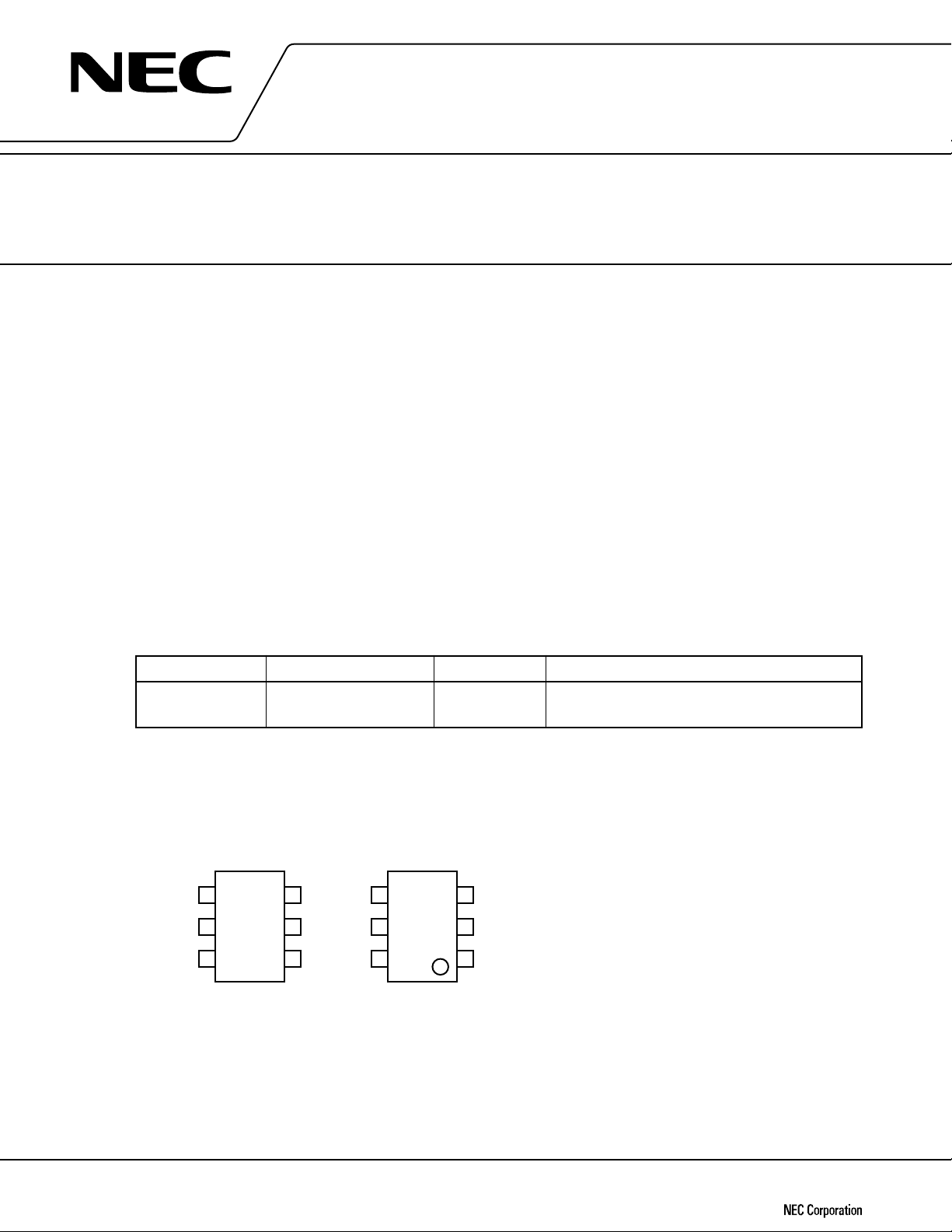
PIN CONNECTIONS
(Top View) (Bottom View)
3
2
1
4
5
C2B
6
4
5
6
3
2
1
1: INPUT
2: GND
3: OUTPUT
4: V
CC
5: C1
6: C2
Document No. P11501EJ2V0DS00
(Previous No. ID-3534)
Date Published May 1996 P
Printed in Japan
Caution Electro-static sensitive devices
©
1996
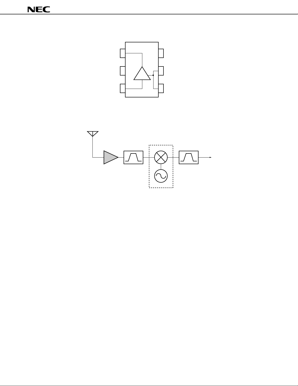
INTERNAL BLOCK DIAGRAM
µ
PC8102T
3
2
1
SYSTEM APPLICATION EXAMPLE AS PAGER
150 MHz to 330 MHz
µ
PC8102T BPF
µ
PC8103T
4
5
6
BPF
IF
2
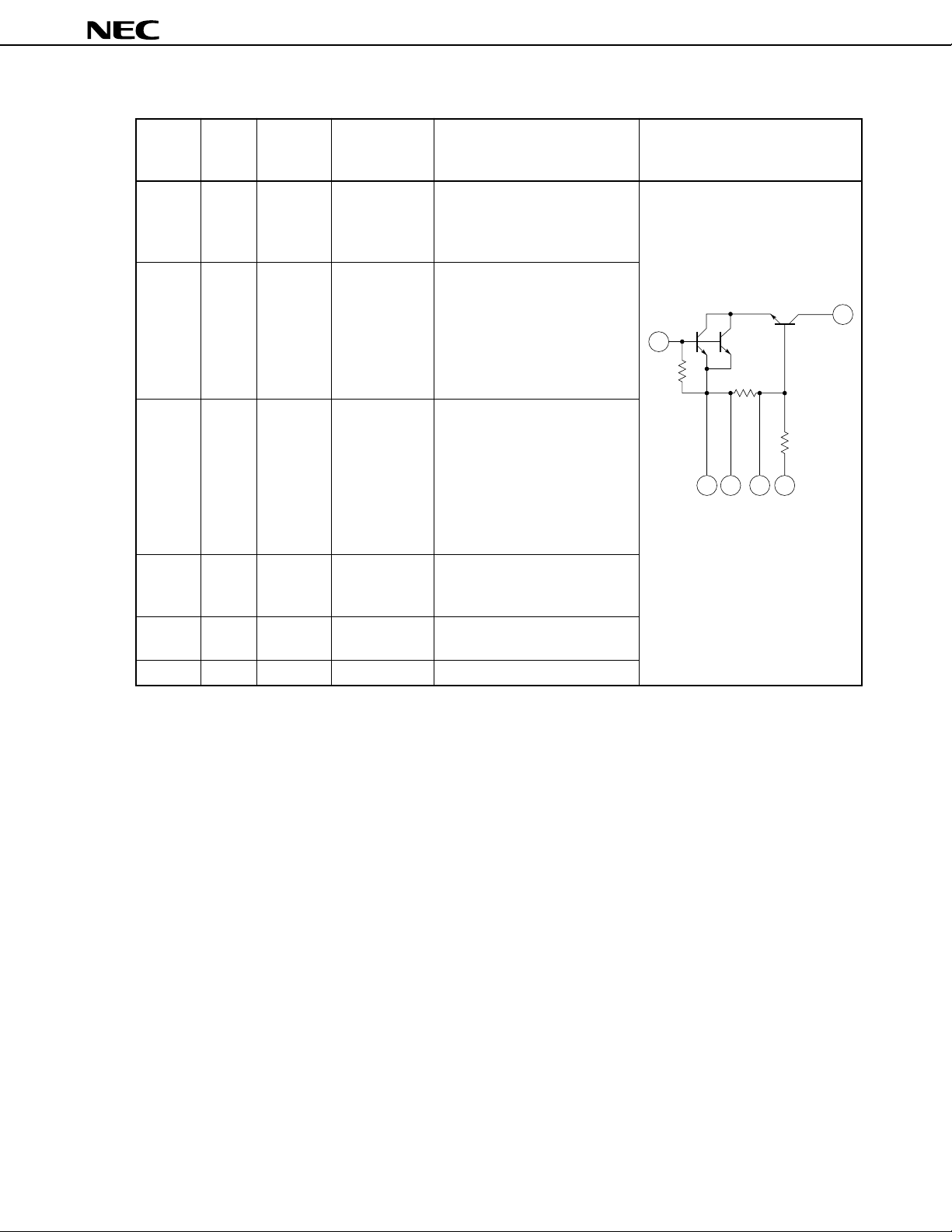
PIN EXPLANATION
1
26 54
3
µ
PC8102T
SUPPLY
PIN NO. NAME VOLTAGE
(V)
1 INPUT — 0.75 RF signal input pin. This pin
2 GND 0 — This ground pin must be
3 OUTPUT — Amplified signal output pin.
4VCC 0.9 to 2.0 — Supply voltage pin. Connect
5 C1 — 0.88 Ground with capacitance pin (eg
6 C2 — 0.85 AC ground pin for output
C2 pin
voltage
must be
applied
through
external
matching
inductor
PIN VOLTAGE
(V)
FUNCTION AND APPLICATION EQUIVALENT CIRCUIT
should be externally equipped
with matching circuit in accordance with desired frequency.
connected to the system ground
with minimum inductance.
Ground pattern on the board
should be formed as wide as
possible. Track length should
be kept as short as possible.
This pin should be externally
equipped with matching circuit
in accordance with desired
frequency.
bypass capacitor (eg 1000 pF)
to minimize ground impedance.
1000 pF).
Note Pin voltage values are described at VCC = 1 V.
3
µ
PC8102T
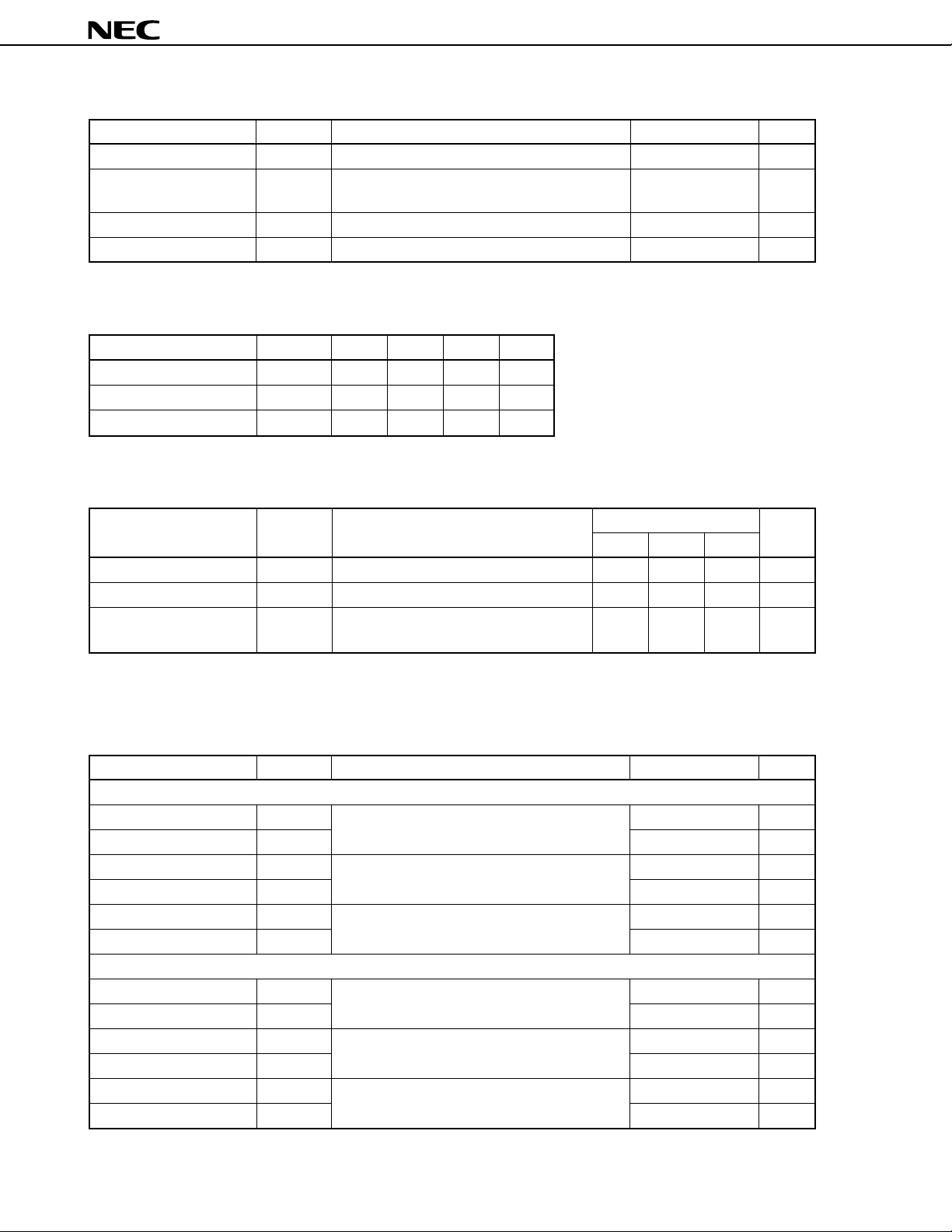
ABSOLUTE MAXIMUM RATINGS
PARAMETER SYMBOL CONDITION RATINGS UNIT
Supply Voltage VCC TA = +25 ˚C 2.2 V
Power Dissipation PD Mounted on 50 × 50 × 1.6 mm double copper 280 mW
clad epoxy glass PWB at TA = +85 ˚C
Operating Temperature Topt –40 to +85 ˚C
Storage Temperature Tstg –55 to +150 ˚C
RECOMMENDED OPERATING CONDITIONS
PARAMETER SYMBOL MIN. TYP. MAX. UNIT
Supply Voltage VCC 0.9 1.0 2.0 V
Operating Temperature Topt –40 +25 +85 ˚C
Operating Frequency fopt 150 330 MHz
Electric characteristic (TA = +25 ˚C, VCC = 1.0 V, ZS = ZL = 50
PARAMETER SYMBOL TEST CONDITIONS
Circuit Current ICC No input signal, TEST CIRCUIT 1 0.30 0.5 0.65 mA
Power Gain GP f = 280 MHz, TEST CIRCUIT 3 10.0 13.5 16.5 dB
Output 3rd order OIP3 f1 = 150.000 MHz, f2 = 150.025 MHz — –5 — dBm
intercept point TEST CIRCUIT 2
ΩΩ
Ω)
ΩΩ
µ
PC8102T
MIN. TYP. MAX.
Note External matching circuits should be attached to input and output pins.
Standared characteristics for reference (Sample: I
PARAMETER SYMBOL CONDITIONS Reference value UNIT
matched with 50 Ω
Power Gain 1 GP1 f = 150 MHz, TEST CIRCUIT 2 20.6 dB
Noise Figure 1 NF1 3.6 dB
Power Gain 2 GP2 f = 280 MHz, TEST CIRCUIT 3 14.7 dB
Noise Figure 2 NF2 4.0 dB
Power Gain 3 GP3 f = 330 MHz, TEST CIRCUIT 5 14.5 dB
Noise Figure 3 NF3 4.1 dB
matched to optimize NF
Power Gain 4 GP4 f = 150 MHz, TEST CIRCUIT 2 19.4 dB
Noise Figure 4 NF4 2.3 dB
Power Gain 5 GP5 f = 280 MHz, TEST CIRCUIT 4 14.0 dB
Noise Figure 5 NF5 2.9 dB
Power Gain 6 GP6 f = 330 MHz, TEST CIRCUIT 6 11.6 dB
Noise Figure 6 NF6 3.1 dB
CC = 0.55 mA, Condition: TA = +25 ˚C, VCC = 1.0 V)
UNIT
4

TEST CIRCUIT 1
123
IN GND OUT
µ
PC8102T
C2 C1 V
654
CC
A
5
µ
PC8102T
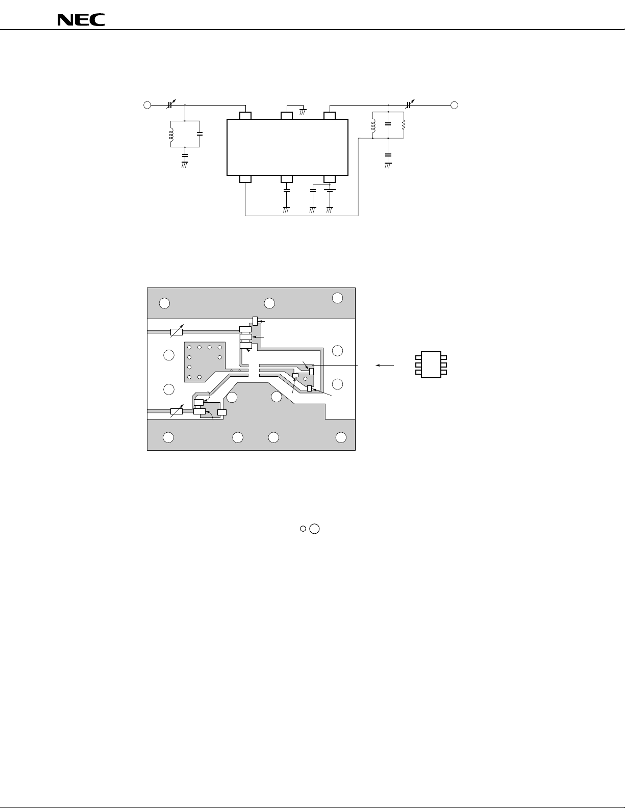
TEST CIRCUIT 2 (150 MHz) <Matched with 50
(Note)
7.5 pF
68 nH
10 pF
1 000 pF
ΩΩ
Ω or matched to optimize NF>
ΩΩ
213
IN
C2
1 000 pF
GND OUT
CCC1
564
1 000
pF
V
84 nH
7.5 pF
10
47 kΩ
pF
1 000 pF
(Note)
Note Matching can be adjusted with trimmer condenser.
ILLUSTRATION OF THE TEST CIRCUIT 2 ASSEMBLED ON EVALUATION BOARD
47k
1 000 pF
84 nH
Ω
1 000 pF
1 000 pF
8102/07
1 000 pF
3
V
CC
2
C2B
1
Mounting direction
OUT
10 pF
7.5pF
10 pF
7.5pF
IN
1 000 pF
68 nH
4
5
6
Note
(*1) 35 × 42 × 0.4 mm double copper clad polyimide board
(*2) Back side: GND pattern
(*3) Solder plated on pattern
: Through holes
(*4)
6
 Loading...