NEC UPC8101GR-E2, UPC8101GR Datasheet

DATA SHEET
BIPOLAR ANALOG INTEGRATED CIRCUIT
µ
PC8101GR
150 MHz SILICON QUADRATURE MODULATOR IC
FOR DIGITAL MOBILE COMMUNICATIONS
DESCRIPTION
µ
PC8101GR is a silicon monolithic integrated circuit designed as up-to-150 MHz quadrature modulator for digital mobile
communications, mainly CT2. This modulator consists of digital 90° phase shifter, dual mixers and various buffer amplifiers
which are packaged in 20 pin SSOP. Up/down converter IC (µPC8100GR) is also available as for kit-use with this IC. So,
these pair devices contribute to make RF block small, high-performance and low power-consumption.
This product is manufactured using NEC’s 20 GHz f
passivation film and gold electrodes. These materials can protect chip surface from external pollution and prevent corrosion
and migration. Thus, this product has excellent performance, uniformity and reliability.
T NESAT
III silicon bipolar process. This process uses silicon nitride
FEATURES
• Operating frequency: fIF = 50 MHz to 150 MHz, Local input frequency: fLo = 100 MHz to 300 MHz, fI/Q = DC to 500 kHz
• Digital 90° phase shifter is incorporated. (Due to the flip flop phase shifter, fIF = fLo/2 + fI/Q.)
• 20 pin SSOP suitable for high-density surface mounting.
• Supply voltage V
• Equipped with Power Save Function.
APPLICATIONS
• Typical application – Digital cordless phone CT2. (In the case of I/Q method)
• Further application – Digital communication equipments.
ORDERING INFORMATION
PART NUMBER PACKAGE SUPPLYING FORM
µ
PC8101GR-E2 20 pin plastic SSOP Embossed tape 12 mm wide. QTY 2.5 kp/Reel.
Remark To order evaluation samples, please contact your local NEC sales office. (Order number: µPC8101GR)
CC = 2.7 to 5.5 V
(225 mil) Pin 1 indicates roll-in direction of tape.
The information in this document is subject to change without notice. Before using this document, please
confirm that this is the latest version.
Not all devices/types available in every country. Please check with local NEC representative for availability
and additional information.
Document No. P10818EJ3V0DS00 (3rd edition)
Date Published October 1999 N CP(K)
Printed in Japan
Caution electro-static sensitive devices
The mark shows major revised points.
©
1995,1999

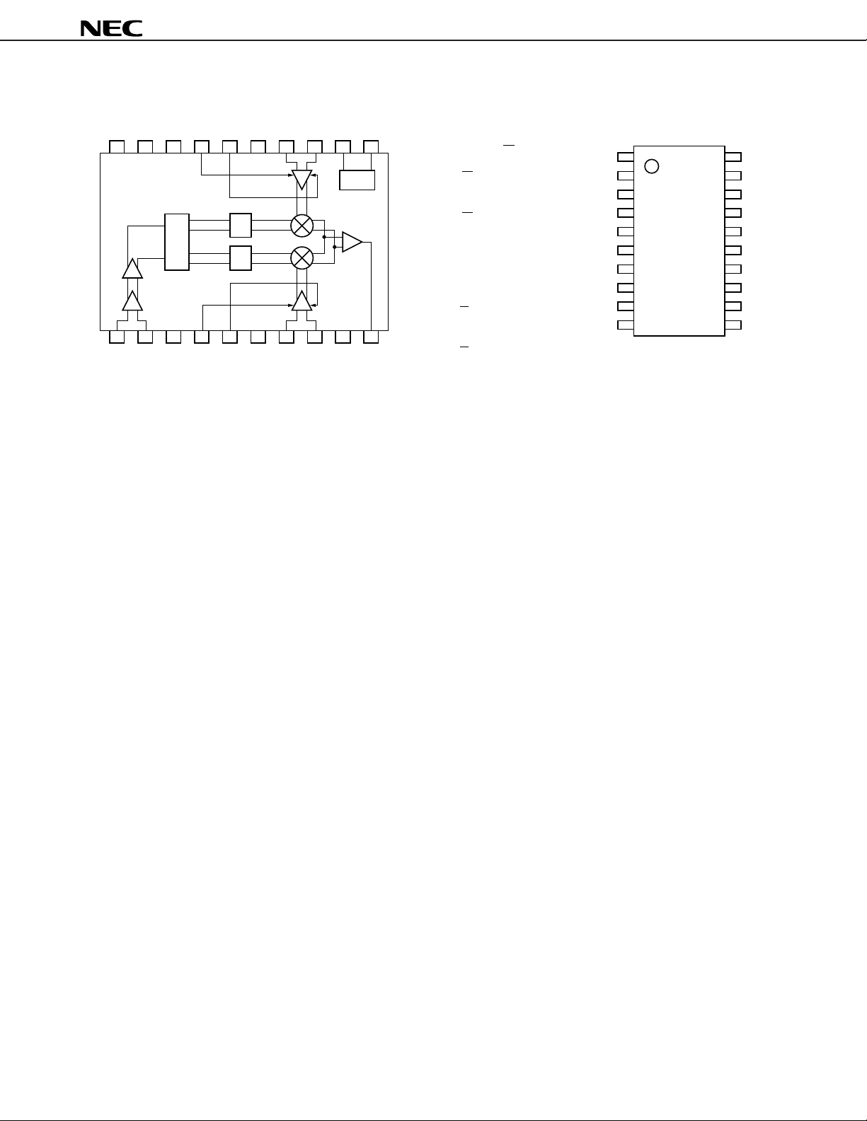
INTERNAL BLOCK DIAGRAM AND PIN CONNECTIONS
µ
PC8101GR
20 19 18 17 16 15 14 13 12
90°
LPF
270°
F / F
0°
180°
LPF
12345678910
11
REG.
1. LOCAL IN
2. LOCAL IN
3. GND
4. Q – BIAS
5. Q – BIAS
6. GND
7. Q – INPUT
8. Q – INPUT
9. GND
10. IF OUTPUT
11. V
CC
12. POWER SAVE
13. I – INPUT
14. I – INPUT
15. GND
16. I – BIAS
17. I – BIAS
18. GND
19. N.C.
20. GND
10
1
2
3
4
5
6
7
8
9
(Top View)
20
19
18
17
16
15
14
13
12
11
2
Data Sheet P10818EJ3V0DS00

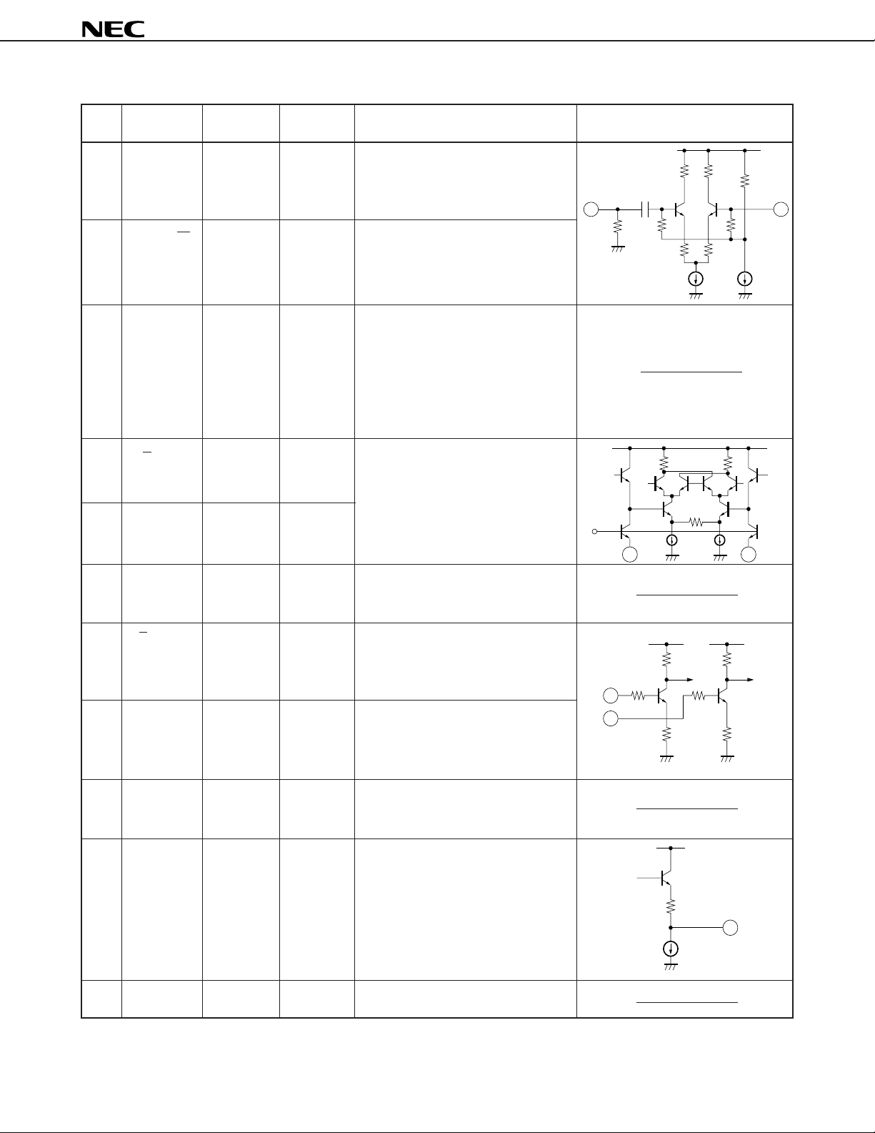
PIN EXPLANATION
µ
PC8101GR
PIN
ASSIGNMENT
NO.
1 LOCAL IN – –
2 LOCAL IN – 2.0
3 GND 0 –
4 Q-BIAS – 0.175
5 Q-BIAS – 0.175
APPLIED
VOLTAGE (V)
PIN VOLTAGE
(V)
FUNCTION AND APPLICATION EQUIVALENT CIRCUIT
Local input for phase shifter.
This input impedance is 50 Ω matched
internally.
Bypass of local buffer amplifier input.
Grounded through capacitor.
It must be connected to the system ground
with minimum inductance. Ground pattern on the board should be formed as
wide as possible.
(Track length should be kept as short as
possible.)
These pins are to adjust local leakage
level.
These pins should be grounded through
register 1 kΩ adjustable 30 mV offset.
1
V
CC
2
6 GND 0 –
7 Q-INPUT VCC/2 –
8 Q-INPUT VCC/2 –
9 GND 0 –
10 IF OUTPUT – 1.4
Track length should be kept as short as
possible.
Input for Q signal. This input impedance
is larger than 500 kΩ. As Q signal, VCC/
2 bias DC signal should be input.
Input for Q signal. This input impedance
is larger than 500 kΩ. As Q signal, VCC/
2 biased 1VP–P signal should be input.
Track length should be kept as short as
possible.
IF output from modulator. This output is
emitter follower as 50 Ω impedance. IF
output frequency is provided as fIF = fLo/
2 + fI/Q.
5
4
7
8
10
11 VCC 2.7 to 5.5 –
Supply voltage pin.
Data Sheet P10818EJ3V0DS00
3

µ
PC8101GR
PIN
ASSIGNMENT
NO.
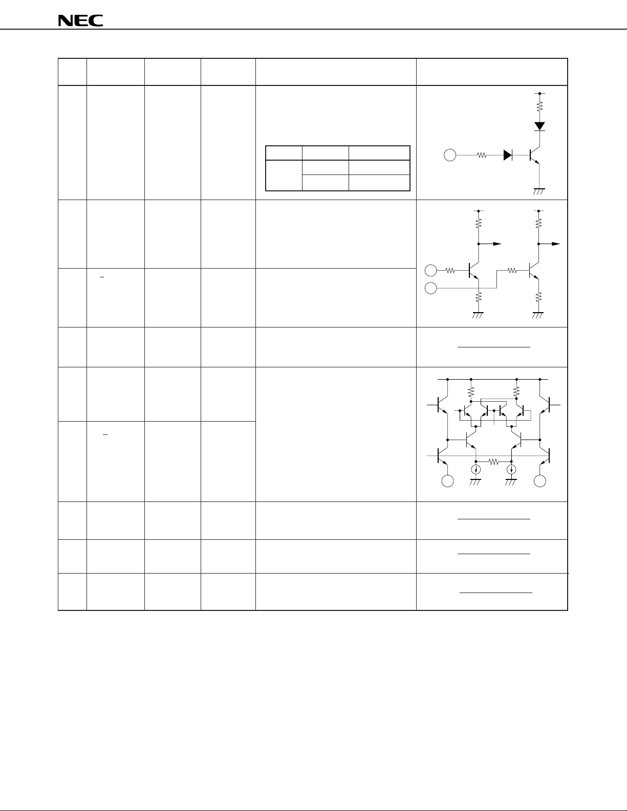
12 POWER 0 to 5.5 –
SAVE
13 I-INPUT VCC/2 –
14 I-INPUT VCC/2 –
15 GND 0 –
APPLIED
VOLTAGE (V)
PIN VOLTAGE
(V)
FUNCTION AND APPLICATION EQUIVALENT CIRCUIT
Power save control pin. This pin can
control ON/OFF operation with bias as
follows;
Bias: V Operation
PS
V
Input for I signal. This input impedance is larger than 500 kΩ. As I signal,
VCC/2 biased 1 VP–P MAX. signal should
be input.
Input for I signal. This input impedance is larger than 500 kΩ. As I signal,
VCC/2 bias DC signal should be input.
Track length should be kept as short
as possible.
≥1.8 ON
0 to 1.0 OFF
12
13
14
16 I-BIAS – 0.175
17 I-BIAS – 0.175
18 GND 0 –
19 N.C – –
20 GND 0 –
* Pin voltage at VCC = 2.7 V
These pins are to adjust local leakage
level.
These pins should be grounded through
register 1 kΩ adjustable 30 mV offset.
Track length should be kept as short
as possible.
Non connection
Track length should be kept as short
as possible.
16
17
4
Data Sheet P10818EJ3V0DS00

µ
PC8101GR
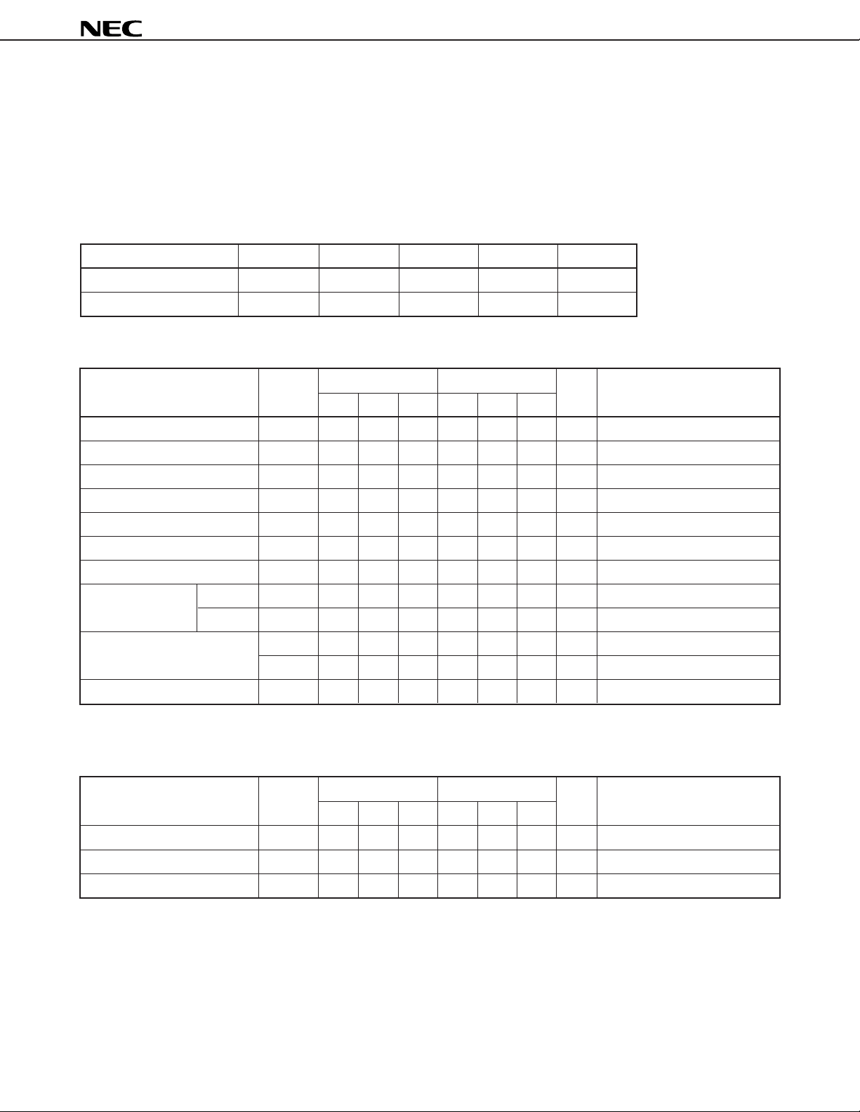
ABSOLUTE MAXIMUM RATINGS
Supply Voltage VCC TA = +25 °C 6.0 V
Power Dissipation PD Mounted on 50 × 50 × 1.6 mm double copper 530 mW
clad epoxy glass board at TA = +70 °C
Operating Temperature Topt –20 to +70 °C
Storage Temperature T
stg –65 to +150 °C
RECOMMENDED OPERATING CONDITIONS
PARAMETER SYMBOL MIN. TYP. MAX. UNIT
Supply Voltage VCC 2.7 3.0 5.5 V
Operating Temperature Topt –20 +25 +70 °C
ELECTRICAL CHARACTERISTICS (TA = +25 °C, UNLESS OTHERWISE SPECIFIED VP/S ≥ 1.8 V)
PARAMETER SYMBOL
Circuit current ICC 10.0 15.0 22.0 17.0 24.5 32.0 mA No input signal
Circuit current power-save mode ICC(P/S) 330 480 1050 1500µAVP/S ≤ 1.0 V
IF output level PIFout –15 –11 –7.0 –12.5 –7.7 –4.5 dBm 50 Ω load, f = fLo/2 + fI/Q*
Local leakage (carrier) ISO(Lo) 26.0 35.0 30.6 dBc f = fLo/2*
Local leak level at IFout pin Loif –49 –37 –39.4 –28 dBm I/Qinput : DC = VCC /2
Image rejection (side band leak) ImR 28.5 37.5 28.5 38.2 dBc f = fLo/2 – fI/Q*
I/Q input impedance ZI/Q 500 1 000 500 700 kΩ I/Qbias = 2.75 V
Power-save
response time
Power-save control voltage VP/S(ON) 1.8 5.5 1.8 5.5 V Normal operation
Local input level PLoin –17 –7 –17 –7 dBm
rise time TP/S(RISE) 1.0 5.0 1.0 5.0
fall time TP/S(FALL) 1.0 3.0 1.0 3.0
VP/S(OFF) 1.0 1.0 V Power-save mode
VCC = 2.7 V VCC = 5.5 V
MIN. TYP. MAX. MIN. TYP. MAX.
UNIT TEST CONDITION
1
1
µ
sVP/S(OFF) → VP/S(ON)
µ
sVP/S(ON) → VP/S(OFF)
STANDARD CHARACTERISTICS FOR REFERENCE
(TA = +25 °C, UNLESS OTHERWISE SPECIFIED VP/S ≥ 1.8 V)
1
PARAMETER SYMBOL
3rd order distortion of I/Q
Local input VSWR VSWRLoin 1.1 1.1 X : 1
IF output VSWR VSWRIFout 1.2 1.2 X : 1
IM3I/Q –37.3 –56.5 dBc f = fLo/2 – 3fI/Q*
VCC = 2.7 V VCC = 5.5 V
MIN. TYP. MAX. MIN. TYP. MAX.
*1 :fLoin = 300.1 MHz PLoin = –10 dBm
f
I/Q = 36 kHz 1 VP-P DC = VCC/2
Data Sheet P10818EJ3V0DS00
UNIT TEST CONDITION
1
5
 Loading...