

DATA SHEET
BIPOLAR ANALOG INTEGRATED CIRCUIT
µ
PC8002
SECOND MIXER + IF AMPLIFIER
FOR DIGITAL CORDLESS TELEPHONES
The µPC8002 is a monolithic IC developed for use in digital cordless telephones. Its internal equivalent circuits
comprise a double balanced mixer (DBM), IF amplifier circuit, and RSSI (Received Signal Strength Indicator) circuit.
µ
PC8002 can operate on a wide range of power supply voltages from 2.7 V to 5.5 V, and incorporates a power-
The
off function, making it ideal for achieving low set power consumption.
The package is a 20-pin plastic shrink SOP (225 mil) suitable for high-density surface mounting.
FEATURES
• Low-voltage, low-consumption-current operation possible (VCC = 2.7 to 5.5 V, ICC = 3.4 mA at VCC = 3 V)
• Wide mixer input frequency range (fMIX = 250 MHz (TYP.) to 500 MHz (MAX.))
• Wide IF amplifier input frequency range (fIF = 8 MHz (MIN.) to 12 MHz (MAX.), 10.7 MHz (TYP.))
• High limiting sensitivity (S
• Wide RSSI dynamic range (DR = 85 dB (TYP.))
• On-chip power-off function
• Use of 20-pin plastic shrink SOP (225 mil) allows high-density surface mounting
L = –100 dBm (TYP.))
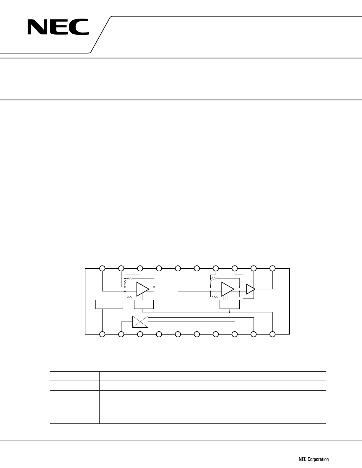
BLOCK DIAGRAM
BYPASS1
Power ON/OFF
IF1 IN19BYPASS218IF1 OUT17BYPASS416IF2 IN15BYPASS3
20
IF Amp 1
RSSI
2nd MIXER
1 1023456789
PD
LO IN
GND(IF) GND(MIX) MIX IN2MIX IN1
ORDERING INFORMATION
Part Number Package
µ
PC8002GR 20-pin plastic shrink SOP (225 mil)
µ
PC8002GR-E1 20-pin plastic shrink SOP (225 mil)
Embossed carrier taping (pin 1 is tape unwinding direction)
µ
PC8002GR-E2 20-pin plastic shrink SOP (225 mil)
Embossed carrier taping (pin 1 is tape winding direction)
14
GND
(IF OUT)
13
IF Amp 2
RSSI
VCC
(IF OUT)
12
Output Stage
IF2 OUT
11
RSSI OUTMIX OUT VCC (IF) VCC (MIX)
The information in this document is subject to change without notice.
Document No. S10717EJ2V0DS00 (2nd edition)
Date Published March 1997 N
Printed in Japan
©
1997

Application Circuit Example 1 (Using 2 BPFs)
V
CC
PD
1
BYPASS1
20
1000 pF
µ
PC8002
BPF
(MURATA)
CFEC10.7MK1
Lo OSC
1st Mixer
V
CC
1000 pF
V
CC
1000 pF
470 pF
470 pF
µ
1 F
1 F
µ
MIX OUT
2
V
3
V
4
LO IN
5
GND (IF)
6
GND (MIX)
7
MIX IN1
8
CC
CC
(IF)
(MIX)
IF1 IN
BYPASS2
IF1 OUT
BYPASS4
IF2 IN
BYPASS3
GND (IF OUT)
19
18
17
16
15
14
13
1000 pF
0.01 F
µ
0.01 F
µ
BPF
(MURATA)
CFEC10.7MK1
470 pF
9
MIX IN2
CC
(IF OUT)
V
12
1000 pF
ADC
10
RSSI OUT
IF2 OUT
11
Caution Ensure that the pin voltage does not exceed the power supply voltage.
Remark The V
CC pass capacitors (1
µ
F, 1000 pF) should be located close to the respective VCC pins.
Chip laminated ceramic capacitors (MURATA GRM36 or equivalent) should be used.
2
1 F
µ
V
CC
DEM
Application Circuit Example 2 (Using 1 BPF)
µ
PC8002
Lo OSC
V
CC
V
CC
1 F
1000 pF
V
CC
1 F
1000 pF
470 pF
1
2
3
PD
MIX OUT
CC
(IF)
V
BYPASS1
IF1 IN
BYPASS2
20
19
18
1000 pF
1000 pF
330 pF
µ
CC
(MIX)
V
4
IF1 OUT
17
µ
LO IN
5
GND (IF)
6
GND (MIX)
7
BYPASS4
BYPASS3
IF2 IN
16
15
14
0.01 F
µ
0.01 F
µ
BPF
(MURATA)
CFEC10.7MK1
1st Mixer
ADC
470 pF
470 pF
8
9
10
MIX IN1
MIX IN2
RSSI OUT
GND (IF OUT)
CC
(IF OUT)
V
IF2 OUT
13
12
1000 pF
11
µ
1 F
Cautions 1. Ensure that the pin voltage does not exceed the power supply voltage.
2. With this application circuit, confirm that there is not problem with interfering wave
characteristics.
Remark The V
CC pass capacitors (1
µ
F, 1000 pF) should be located close to the respective VCC pins.
Chip laminated ceramic capacitors (MURATA GRM36 or equivalent) should be used.
V
CC
DEM
3
Application Circuit Example 3 (Using 1 BPF)
V
CC
PD
1
BYPASS1
20
1000 pF
µ
PC8002
BPF
(MURATA)
CFEC10.7MK1
Lo OSC
1st Mixer
V
CC
1000 pF
V
CC
1000 pF
470 pF
470 pF
µ
1 F
1 F
µ
MIX OUT
2
V
3
V
4
LO IN
5
GND (IF)
6
GND (MIX)
7
MIX IN1
8
CC
(IF)
CC
(MIX)
IF1 IN
BYPASS2
IF1 OUT
BYPASS4
IF2 IN
BYPASS3
GND (IF OUT)
19
18
17
16
15
14
13
1000 pF
390 Ω
µ
0.01 F
1000 pF
0.01 F
µ
V
1 F
µ
CC
ADC
470 pF
9
10
MIX IN2
RSSI OUT
CC
(IF OUT)
V
IF2 OUT
12
1000 pF
11
Cautions 1. With this application circuit, good interfering wave characteristics are obtained with a single
BPF. However, there is a drop in sensitivity.
2. Ensure that the pin voltage does not exceed the power supply voltage.
Remark The V
CC pass capacitors (1
µ
F, 1000 pF) should be located close to the respective VCC pins.
Chip laminated ceramic capacitors (MURATA GRM36 or equivalent) should be used.
4
DEM
Application Circuit Example 4 (Using 1 BPF)
V
Lo OSC
CC
V
CC
1000 pF
V
CC
1000 pF
470 pF
1 F
µ
1 F
µ
1
2
3
4
5
PD
MIX OUT
CC
(IF)
V
V
CC
(MIX)
LO IN
BYPASS1
IF1 IN
BYPASS2
IF1 OUT
BYPASS4
20
19
18
17
16
1000 pF
1000 pF
390 Ω
µ
0.01 F
µ
PC8002
BPF
(MURATA)
CFEC10.7MK1
1000 pF
GND (IF)
1st Mixer
ADC
470 pF
470 pF
6
7
8
9
10
GND (MIX)
MIX IN1
MIX IN2
RSSI OUT
BYPASS3
GND (IF OUT)
CC
(IF OUT)
V
IF2 OUT
IF2 IN
15
14
13
12
1000 pF
11
µ
1 F
1000 pF
µ
0.01 F
V
CC
µ
1.5 H
150 pF
DEM
Cautions 1. With this application circuit, good interfering wave characteristics are obtained with a single
BPF (and sensitivity is better than in Application Circuit Example 3).
2. Ensure that the pin voltage does not exceed the power supply voltage.
Remark The V
Chip laminated ceramic capacitors (MURATA GRM36 or equivalent) and a chip coil (MURATA LQHIN
or equivalent) should be used.
CC pass capacitors (1
µ
F, 1000 pF) should be located close to the respective VCC pins.
5

µ
PC8002
CONTENTS
1. PIN CONFIGURATION AND PIN FUNCTIONS....................................................................................7
2. INPUT/OUTPUT EQUIV ALENT CIRCUIT DIAGRAMS ........................................................................9
3. ELECTRICAL SPECIFICATIONS .......................................................................................................10
4. CHARACTERISTIC DIAGRAMS ........................................................................................................13
5. LEVEL DIAGRAMS.............................................................................................................................17
6. TEST METHODS ................................................................................................................................18
7. TEST CIRCUIT EXAMPLES ...............................................................................................................19
8. EV ALUATION BOARD MOUNTING EXAMPLE .................................................................................25
9. WIRING P A TTERN CAPACITANCE DIAGRAM (REFERENCE) ........................................................28
10. P ACKAGE DRA WINGS.......................................................................................................................29
11. RECOMMENDED SOLDERING CONDITIONS..................................................................................30
6
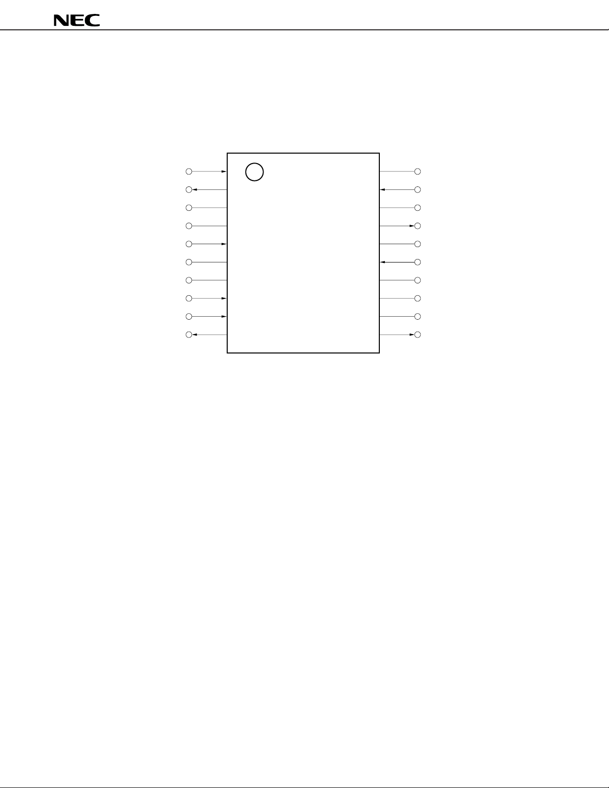
1. PIN CONFIGURATION AND PIN FUNCTIONS
(1) Pin Configuration (Top View)
• 20-pin plastic shrink SOP (225 mil)
µ
PC8002
PD
MIX OUT
V
CC
(IF)
CC
(MIX)
V
LO IN
GND (IF)
GND (MIX)
MIX IN1
MIX IN2
RSSI OUT
1
2
3
4
5
6
7
8
9
10
20
19
18
17
16
15
14
13
12
11
Pin Names
BYPASS1-BYPASS4 : Bypass
GND (IF) : Ground (Intermediate Frequency Amp.)
GND (IF OUT) : Ground (Intermediate Frequency Amp. Output)
GND (MIX) : Ground (Mixer)
IF1 IN, IF2 IN : Intermediate Frequency Amp. Input
IF1 OUT, IF2 OUT : Intermediate Frequency Amp. Output
LO IN : Local Input
MIX IN1, MIX IN2 : Mixer Input
MIX OUT : Mixer Output
PD : Power Down
RSSI OUT : Received Signal Strength Indicator Output
CC (IF) : Power Supply (Intermediate Frequency Amp.)
V
VCC (IF OUT) : Power Supply (Intermediate Frequency Amp. Output)
VCC (MIX) : Power Supply (Mixer)
BYPASS1
IF1 IN
BYPASS2
IF1 OUT
BYPASS4
IF2 IN
BYPASS3
GND (IF OUT)
CC
(IF OUT)
V
IF2 OUT
7

(2) Pin Functions
No. Pin Name I/O Function
1 PD I Power on/off control signal input
2 MIX OUT O Mixer output
3VCC (IF) – IF amplifier and RSSI power supply pin
4VCC (MIX) – Mixer power supply pin
5 LO IN I Local input
6 GND (IF) – IF amplifier and RSSI ground pin
7 GND (MIX) – Mixer ground pin
8 MIX IN1 I Mixer input
9 MIX IN2 I Filter capacitor connection
10 RSSI OUT O RSSI output
11 IF2 OUT O IF amplifier 2 output
12 VCC (IF OUT) – IF amplifier output stage power supply pin
13 GND (IF OUT) – IF amplifier output stage ground pin
14 BYPASS3 – Filter capacitor connection (IF2 side)
15 IF2 IN I IF amplifier 2 input
16 BYPASS4 – Filter capacitor connection (IF2 side)
17 IF1 OUT O IF amplifier 1 output
18 BYPASS2 – Filter capacitor connection (IF1 side)
19 IF1 IN I IF amplifier 1 input
20 BYPASS1 – Filter capacitor connection (IF1 side)
µ
PC8002
8
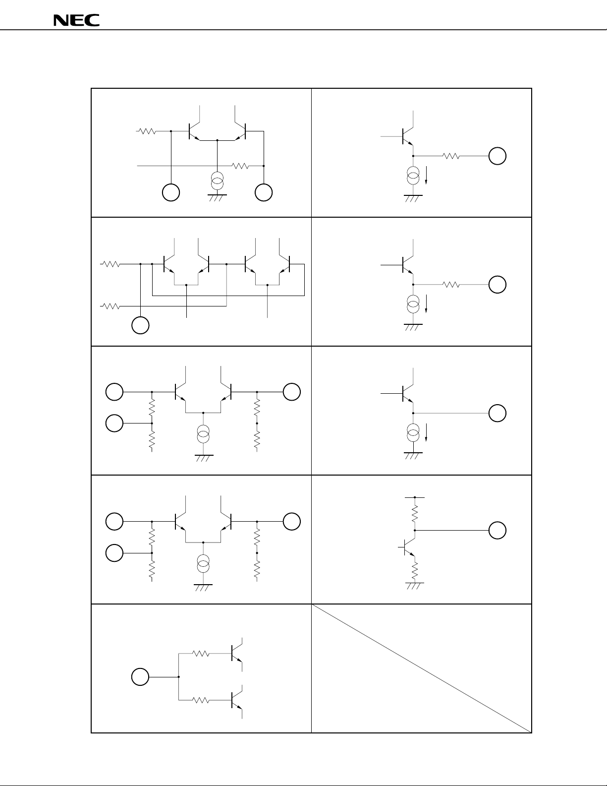
2. INPUT/OUTPUT EQUIVALENT CIRCUIT DIAGRAMS
µ
PC8002
Mixer Input
1 kΩ
Local Input
1 kΩ
1 kΩ
5
IF Amplifier 1 Input
Mixer Output
276 Ω
1 kΩ
700 A
µ
8
9
2
IF Amplifier 1 Output
207 Ω
µ
250 A
17
IF Amplifier 2 Output
19
330 Ω
18
14.9 kΩ
IF Amplifier 2 Input
15
330 Ω
14
11.8 kΩ
Power On/Off Input
1
50 kΩ
150 kΩ
330 Ω
14.9 kΩ
330 Ω
11.8 kΩ
20
16
RSSI Output
V
CC
32 kΩ
2 kΩ
290 A
µ
11
10
9
µ
PC8002
3. ELECTRICAL SPECIFICATIONS
Absolute Maximum Ratings (TA = 25 °C)
Parameter Symbol Test Condition Rating Unit
Power supply voltage VCC 7V
Total power dissipation PT TA = 85 °C 120 mW
Storage temperature Tstg –40 to +125 °C
Pin voltage VPIN VCC+0.2 V
Caution Product quality may suffer if the absolute rating is exceeded for any parameter, even momentarily.
In other words, an absolute maximum rating is a value at which the possibility of physical damage
to the product cannot be ruled out. Care must therefore be taken to ensure that the these ratings
are not exceeded during use of the product.
Recommended Operating Ratings (T
Parameter Symbol Test Condition MIN. TYP. MAX. Unit
Power supply voltage VCC 2.7 3.0 5.5 V
Operating ambient temperature TA –30 +25 +85 °C
Mixer input level VMIX 50 Ω resistance termination –98 –18 dBm
Local input level VLOC 50 Ω resistance termination –5 +5 dBm
IF amplifier input level VIF –99 –14 dBm
Mixer input frequency fMIX 250 500 MHz
Mixer output frequency fOM 8 10.7 12 MHz
IF amplifier input frequency fIF 8 10.7 12 MHz
RSSI output load capacitance COI 10
IF2 output load capacitance COR 10
A = 25 °C) 0 dBm = 223.6 mVrms (at 50 Ω)
LC matching (reference value) –107 –27
LC matching (reference value) –20 –10
Note
Note
Note Includes all capacitances (board, pattern, etc.) applied to the pin.
pF
pF
10

Electrical Specifications (TA = 25 °C, VCC = 3 V)
µ
PC8002
(1) Mixer Section (f
MIX = 250 MHz, fLOC = 239.3 MHz, VLOC = –5 dBm) 0 dBm = 223.6 mVrms (at 50 Ω)
(Where not specified in the Test Condition, input has 50 Ω termination)
Parameter Symbol Test Condition MIN. TYP. MAX. Unit
Power supply current ICCM No signal 1.7 2.2 mA
Conversion gain GC 50 Ω resistance termination 4 8 11.0 dB
LC matching (reference value) 17.0
–1 dB compression output level VOM –14 –10 –7 dBm
Third order intercept point IP3 Stipulated by output Note 1 –3 dBm
Noise factor NF 16 dB
LC matching (reference value) 7 dB
Local separation ISL Mixer non-input Note 2 40 54 dB
Mixer input impedance ZINM 31-j156 Ω
Local input impedance ZINL 31-j169 Ω
Output resistance ROM 230 330 430 Ω
Power-on rise time tONM VPO = 3 V
Power-off fall time tOFM VPO = 0 V
Power-off power supply current ILM VPO = 0 V 0 5
Note 3
Note 4
815
13
Notes 1. f1 = 250.3 MHz, f2 = 250.6 MHz
2. Leakage from local input to mixer output
3. Time until the difference between the local input pin power-on and power-off voltages reaches 90 %
Power-on input voltage (V
PO) rise time: 10 ns
4. Time until the power supply current reaches 10 % of the power-on value
Power-on input voltage (V
PO) fall time: 10 ns
µ
s
µ
s
µ
A
11

µ
PC8002
(2) IF Amplifier Section (fIF = 10.7 MHz) 0 dBm = 223.6 mVrms (at 50 Ω)
Parameter Symbol Test Condition MIN. TYP. MAX. Unit
Power supply current ICCI No signal 1.7 2.3 mA
Limiting sensitivity SL –3 dB point –100 –97 dBm
IF amplifier phase fluctuation SP VIF = –70 to –14 dBm Note 1 10 deg
IF amplifier output amplitude VO IF2 OUT, VIF = –14 dBm 0.2 0.3 0.4 Vp-p
IF amplifier output amplitude rise time
IF amplifier output amplitude fall time tF IF2 OUT, VIF = –14 dBm 15 25 ns
IF amplifier input resistance Rin IF1 IN, IF2 IN 230 330 430 Ω
IF amplifier input capacitance Cin IF1 IN, IF2 IN 3.5 6.0 pF
IF amplifier output resistance RO IF1 OUT 230 330 430 Ω
RSSI linearity LR VIF = –94 to –14 dBm ±2dB
RSSI slope SR 18 20 22 mV/dB
RSSI intercept IR –164.7 –148 –134.4 dBm
RSSI output voltage 1 VR1 VIF = –14 dBm 2.58 2.68 2.78 V
RSSI output voltage 2 VR2 VIF = –54 dBm 1.76 1.88 2.0 V
RSSI output voltage 3 VR3 VIF = –94 dBm 0.88 1.08 1.28 V
RSSI output voltage 4 VR4 No signal 0.96 1.23 V
RSSI output temperature stability ST VIF = –94 to –14 dBm Note 2 ±2dB
RSSI output dynamic range DR Note 3 80 90 dB
RSSI rise time trf1 VIF = –14 dBm Note 4 1.0 4
RSSI fall time trf2 VIF = –14 dBm Note 4 1.6 4
RSSI output ripple RR VIF = –14 dBm 20 mVp-p
RSSI output resistance ROR 25.6 32 38.4 kΩ
Power-on rise time tONI VPO = 3 V, no signal
Power-off fall time tOFI VPO = 0 V
Power-off power supply current ILI VPO = 0 V 6 10
tR IF2 OUT, VIF = –14 dBm 8 20 ns
µ
µ
Note 5
Note 6
510
13
µ
µ
µ
s
s
s
s
A
Notes 1. Network analyzer RBW = 3 Hz
A = –30 °C to +85 °C
2. T
3. Input level range for which drift from the regression expression with VIF = –94 to –14 dBm is ≤ 2 dB
4. Time until the RSSI output reaches the final value ±10 %
5. Time until the RSSI output is within ±10 % of the power-on value
Power-on input voltage (V
PO) rise time: 10 ns
6. Time until the power supply current reaches 10 % of the power-on value
Power-on input voltage (V
PO) fall time: 10 ns
(3) Power-On/Off Section
Parameter Symbol Test Condition MIN. TYP. MAX. Unit
Power-on input voltage VON Power-on at VON or above, VCC or below 1.5 2.4 V
Power-off input voltage VOF Power-off at VOF or below, GND or above 0.6 1.2 V
Power-on input current ION VPO = 3 V 40 60
12
µ
A

4. CHARACTERISTIC DIAGRAMS
(1) Power supply current vs power supply voltage (IF amplifier section)
4
3
2
[mA]
Power supply current
1
µ
PC8002
0
01234567
[V]
Power supply voltage
(2) Power supply current vs power supply voltage (Mixer section)
5
4
3
[mA]
2
Power supply current
1
0
01234567
[V]
Power supply voltage
13

(3) IF amplifier output level vs IF amplifier input level
0
_
3dB
_
10
[dBm]
_
20
IF amplifier output level
µ
PC8002
_
30
_
120
Limiting sensitivity
_
100
_
80
IF amplifier input level
_
[dBm]
(4) IF amplifier output phase vs IF amplifier input level
140
130
120
[deg]
Phase fluctuation
110
Input/output phase difference
100
_
70
_
60
Test input level range
_
50
IF amplifier input level
_
[dBm]
60
40
_
40 0
_
30
_
20
_
20
_
14
_
10
14

(5) RSSI characteristics (a)
3
2.5
2
1.5
[V]
1
RSSI output voltage
0.5
µ
PC8002
Regression line
0
_
120
Regression line
(6) RSSI characteristics (b)
5
4
3
2
1
0
[dB]
_
RSSI error
1
_
2
_
3
_
4
_
5
_
120
_
100 0
_
100 0
_
80
_
80
IF amplifier input level
_
60
[dBm]
IF amplifier input level
_
60
[dBm]
_
40
_
40
_
20
_
20
15

(7) Mixer output level vs mixer input level
µ
PC8002
0
_
10
_
20
_
30
_
40
[dBm]
_
50
Mixer output level
_
60
_
70
_
80
_
70
50 Ω resistance termination
[dBm]
_
30
_
20
_
10
_
60 0
_
50
_
40
Mixer input level
16

5. LEVEL DIAGRAMS
(1) For Application Circuit 1
µ
PC8002GR
µ
PC8002
MIXER
Note 1
+ 8 dB
Note 2
+ 17 dB
18 dBm
27 dBm
Note 1
Note 2
_
_
80 dB
98 dBm
Note 1
Note 2
_
_
107 dBm
(2) For Application Circuit 2
µ
PC8002GR
_
10 dBm
_
90 dBm
BPF
_
4 dB
_
14 dBm
80 dB
_
94 dBm
IF Amp1
+ 42 dB
_
12 dBm
_
52 dBm
BPF
_
4 dB
_
16 dBm
_
56 dBm
IF Amp2
+ 66 dB
IF OUT
0.3 V
_
6.5 dBm
p-p
MIXER
Note 1
+ 8 dB
Note 2
+ 17 dB
_
10 dBm
_
18 dBm
_
27 dBm
Note 1
Note 2
80 dB
_
98 dBm
_
107 dBm
Note 1
Note 2
_
90 dBm
Notes 1. 50 Ω resistance termination
2. LC matching (reference value)
330 pF
80 dB
IF Amp1
+ 42 dB
_
12 dBm
_
48 dBm
BPF
_
4 dB
_
16 dBm
_
52 dBm
IF Amp2
+ 66 dB
IF OUT
0.3 V
_
6.5 dBm
p-p
17

6. TEST METHODS
(1) Mixer input section
(a) With 50 Ω resistance termination (b) With 50 Ω LC matching
µ
PC8002
470 pF
MIX IN1
V
MIX
50 Ω
V
MIX
Note
C
Note
L
470 pF
Note Since the values of L and C are affected by the board’s parasitic capacitance and inductance, L and
C should be adjusted so that the impedance looking at the MIX IN pin side from the signal source is
50 Ω.
(2) Third order intercept
MIX IN1
8
MIX OUT
2
LO IN
5
88
MIX IN1
18
470 p
50 Ω
V
16.7 Ω
16.7 Ω
f1 = 250.3 MHz f2 = 250.6 MHz
MIX
16.7 Ω
82 pF
f
OSC
= 239.3 MHz
470 p
50 Ω

7. TEST CIRCUIT EXAMPLES
In test circuit example 2 onward, only the portion that differs from test circuit example 1 is shown.
Test Circuit Example 1.
µ
PC8002
VCC
VCC
VCC
50 Ω
µ
1 F
µ
1 F
82 pF
1000 pF
1000 pF
470 pF
1
2
3
4
5
6
PD
MIX OUT
CC (IF)
V
CC (MIX)
V
LO IN
GND (IF)
BYPASS1
IF1 IN
BYPASS2
IF1 OUT
BYPASS4
IF2 IN
20
19
18
17
16
15
330 pF
1000 pF
50 Ω
1000 pF
0.01 F
µ
BPF
(MURATA)
CFEC10.7MK1
50 Ω
470 pF
470 pF
10 pF
7
8
9
10
GND (MIX)
MIX IN1
MIX IN2
RSSI OUT
BYPASS3
GND (IF OUT)
CC (IF OUT)
V
IF2 OUT
14
13
12
11
1000 pF
0.01 F
µ
1 F
µ
1000 pF
10 pF
10 kΩ
VCC
Caution The 10 pF capacitor value for IF2 OUT and RSSI OUT includes all the capacitances (board,
pattern, etc.) applied to the pin. Ensure that the recommended load condition (10 pF) is not
exceeded for IF2 OUT and RSSI OUT.
Remark Chip laminated ceramic capacitors (MURATA GRM36 or equivalent) should be used.
19

Test Circuit Example 2. (Power supply current, power-off power supply current)
CC
(IF)
V
3
CC
(IF OUT)
V
12
V
CC
(MIX)
4
µ
PC8002
1000 pF
A
1000 pF1 F
µ
V
CC
A
µ
1000 pF1 F
V
CC
Test Circuit Example 3. (Limiting sensitivity, IF amplifier output amplitude, IF amplifier output amplitude rise
time, IF amplifier output amplitude fall time, RSSI linearity, RSSI slope, RSSI
intercept, RSSI output voltage, RSSI temperature stability, RSSI output ripple)
IF1 IN
19
330 pF
50 Ω
SG (Signal generator)
10.7 MHz
10 pF
RSSI OUT
10
Digital voltmeter
Oscilloscope
IF2 OUT
11
1000 pF
10 kΩ
10 pF
Spectrum
analyzer
Oscilloscope
Caution The 10 pF capacitor value for IF2 OUT and RSSI OUT includes all the capacitances (board,
pattern, etc.) applied to the pin. Ensure that the recommended load condition (10 pF) is not
exceeded for IF2 OUT and RSSI OUT.
20

Test Circuit Example 4. (IF amplifier phase fluctuation)
µ
PC8002
330 pF
50 Ω
IF1 IN
19
Attenuator
Network
analyzer
IF2 OUT
11
1000 pF
10 pF
10 kΩ
Caution The 10 pF capacitor value for IF2 OUT includes all the capacitance (board, pattern, etc.) applied
to the pin. Ensure that the recommended load condition (10 pF) is not exceeded.
Test Circuit Example 5. (RSSI rise time, RSSI fall time)
... Time until RSSI output is within
IF1 IN
19
IF1 OUT
17
±10 % of the final value)
IF2 IN
15
RSSI OUT
10
330 pF
50 Ω
SG
10.7 MHz, _14 dBm
Input signal from SG
1 SEC 50 SEC
Storage
oscilloscope 1
µ
330 pF
50 Ω
SG
10.7 MHz, _14 dBm
10 pF
For IF2 input
Storage
oscilloscope 2
For IF1 input
Caution The 10 pF capacitor value for RSSI OUT includes all the capacitances (board, pattern, etc) applied
to the pin.
21

Test Circuit Example 6. (Power-on rise time)
Mixer section : Time until the difference between the local input pin power-on and
power-off voltage reaches 90 %
IF section : Time until RSSI output is within
µ
±10 % of the power-on value.
PC8002
LO IN
5
RSSI OUT
10
10 pF
Storage
oscilloscope 2
0 V
PD
1
SG
Input signal from SG
3 V
1 SEC
Storage
oscilloscope 1
µ
50 SEC
Remark Power-on input voltage (VPO) rise time: 10 ns
Caution The 10 pF capacitor value for RSSI OUT includes all the capacitances (board, pattern, etc.)
applied to the pin. Ensure that the recommended load condition (10 pF) is not exceeded.
Test Circuit Example 7. (Power-off fall time)
CC
PD
1
SG
Input signal from SG
3 V
0 V
1 SEC
(IF OUT)
V
12
Storage
oscilloscope
µ
50 SEC
CC
V
V
CC
Current probe
(IF)
3
V
V
CC
CC
(MIX)
4
22

Test Circuit Example 8. (Conversion gain, –1 dB compression level)
µ
PC8002
MIX OUT
2
82 pF
50 Ω
Spectrum
analyzer
LO IN
5
470 pF
SG
239.3 MHz
Test Circuit Example 9. (Third order intercept output level)
MIX OUT
2
82 pF
50 Ω
LO IN
5
470 pF
MIX IN1
8
470 pF
See 6. TEST METHODS (1)
SG
250 MHz
MIX IN1
8
470 pF
See 6. TEST METHODS (2)
Spectrum
analyzer
Test Circuit Example 10. (Local separation)
MIX OUT
2
82 pF
Spectrum
analyzer
SG
239.3 MHz
LO IN
5
470 pF
50 Ω
SG
239.3 MHz
23

Test Circuit Example 11. (Power-on input voltage, power-off input voltage, power-on input current)
PD
1
A
V
V
CC
Test Circuit Example 12. (Noise factor)
µ
PC8002
82 pF
MIX OUT
NF meter
470 pF
50 Ω
LO IN
52 8
470 pF
Noise Source
MIX IN1
See 6. TEST METHODS (1)
24

Remark indicates a through-hole.
50 mm
VCC
C2
C3
C1
70 mm
1
PC8002
µ
8. EVALUATION BOARD MOUNTING EXAMPLE
C5
25
C4
KC-8002GR
C6
Plated wire
IF2 OUT
C7 R1
µ
PC8002

26
Remark indicates a through-hole.
IF1 IN
IF2 OUT
R2
BPF
C
8
C9
BPF
C
C11
10
MIX OUT
VCC
1
C
C
9
C10
C12
C
13
10
C11
R4
RSSI OUT
R3
LOCAL IN
L2
L1
MIX IN
µ
PC8002

µ
PC8002
C1 : 1 µF R1 : 10 kΩ
C2 : 1000 pF R2 : 50 Ω
C3 : 1000 pF R3 : 50 Ω
µ
C4 : 1
C5 : 1 µF L1 : 58 nH (reference value)
C6 : 1000 pF L2 : 10 nH (reference value)
C7 : 10 pF
C8 : 330 pF
C9 : 0.01
C10 : 0.01 µF
C11 : 470 pF
C12 : 470 pF
C13 : 10 pF
Note For the IF2 OUT and RSSI OUT capacitance values, see 9. WIRING PATTERN CAPACITANCE DIAGRAM
Remarks 1. Both L in the case of LC matching and R in the case of 50 Ω termination are connected to MIX IN.
F R4 : 50 Ω
Note
µ
F
Note
(REFERENCE).
Remove
2. Change the location of the plated wires according to the evaluation items.
3. Cut the wiring pattern to connect
in the case of LC matching, and and in the case of 50 Ω termination.
R4
L2
.
L1
L2
27

9. WIRING PATTERN CAPACITANCE DIAGRAM (REFERENCE)
The wiring pattern capacitances to ground are shown here.
For pin 11, the capacitance is 8.1 pF when the entire pattern (from pin 11 to point B) is used. In this case,
the usable probe input capacitance is 1.9 pF (MAX.).
From pin 11 up to point A, the capacitance is 1.4 pF, and therefore an 8.6 pF (MAX.) probe can be used.
For pin 10, the capacitance is 4 pF when the entire pattern is used.
µ
PC8002
Pin 11
0.9 pF 0.5 pF
Pin 10
A
IF2 OUT
3.0 pF
2.9 pF
0.8 pF
B
28
RSSI OUT

10. PACKAGE DRAWINGS
20 PIN PLASTIC SHRINK SOP (225mil)
µ
PC8002
20
110
GE
F
C
D
11
A
K
N
B
M
M
detail of lead end
P
H
I
J
L
NOTE
Each lead centerline is located within 0.10 mm (0.004 inch) of
its true position (T.P.) at maximum material condition.
ITEM MILLIMETERS INCHES
A
7.00 MAX.
B
0.575 MAX.
C
0.65 (T.P.)
D
E
F
G
H
I
J
K
L 0.5±0.2 0.020
M
P3˚ 3˚
+0.10
0.22
–0.05
0.1±0.1
1.45 MAX.
1.15±0.1
6.4±0.2
4.4±0.1
1.0±0.2
+0.10
0.15
–0.05
0.10
0.10N 0.004
+7˚
–3˚
0.276 MAX.
0.023 MAX.
0.026 (T.P.)
+0.004
0.009
–0.003
0.004±0.004
0.057 MAX.
+0.005
0.045
–0.004
0.252±0.008
+0.005
0.173
–0.004
+0.009
0.039
–0.008
+0.004
0.006
–0.002
+0.008
–0.009
0.004
+7˚
–3˚
P20GR-65-225C-1
29

11. RECOMMENDED SOLDERING CONDITIONS
The following conditions ( see table below) must be met when soldering this product.
For more details, refer to our document "SEMICONDUCTOR DEVICE MOUNTING TECHNOLOGY
MANUAL" (C10535E).
Please consult with our sales offices in case other soldering process or condition is used.
TYPE OF SURFACE MOUNT DEVICE
µ
PC8002GR
µ
PC8002
Soldering process
Infrared Ray Reflow
VPS
Partial heating
method
Note Exposure limit before soldering after dry-pack package is opened.
Storage conditions : 25 ˚C and relative humidity at 65 % or less.
Caution Do not apply more than one soldering method at any one time, except for " Partial heating
method".
Peak package's surface temperature: 235 ˚C or below.
Reflow time : 30 seconds or below (210 ˚C or higher),
Number of reflow processes : MAX.2
Note
Exposure limit
(10 hours pre-baking is required at 125 ˚C afterwards)
Peak package's temperature: 215 ˚C or below.
Reflow time : 40 seconds or below (200 ˚C or higher),
Number of reflow processes : MAX. 2
Exposure limit
(10 hours pre-baking is required at 125 ˚C afterwards)
Terminal temperature : 300 ˚C or below,
Time : 3 seconds or below (Per side of pin position)
: 7 days
Note
: 7 days
Soldering conditions
Symbol
IR35-107-2
VP15-107-2
30

[MEMO]
µ
PC8002
31

µ
PC8002
The application circuits and their parameters are for references only and are not intended for use in actual design-in's.
No part of this document may be copied or reproduced in any form or by any means without the prior written
consent of NEC Corporation. NEC Corporation assumes no responsibility for any errors which may appear in
this document.
NEC Corporation does not assume any liability for infringement of patents, copyrights or other intellectual property
rights of third parties by or arising from use of a device described herein or any other liability arising from use
of such device. No license, either express, implied or otherwise, is granted under any patents, copyrights or other
intellectual property rights of NEC Corporation or others.
While NEC Corporation has been making continuous effort to enhance the reliability of its semiconductor devices,
the possibility of defects cannot be eliminated entirely. To minimize risks of damage or injury to persons or
property arising from a defect in an NEC semiconductor device, customers must incorporate sufficient safety
measures in its design, such as redundancy, fire-containment, and anti-failure features.
NEC devices are classified into the following three quality grades:
"Standard", "Special", and "Specific". The Specific quality grade applies only to devices developed based on a
customer designated "quality assurance program" for a specific application. The recommended applications of
a device depend on its quality grade, as indicated below. Customers must check the quality grade of each device
before using it in a particular application.
Standard: Computers, office equipment, communications equipment, test and measurement equipment,
audio and visual equipment, home electronic appliances, machine tools, personal electronic
equipment and industrial robots
Special: Transportation equipment (automobiles, trains, ships, etc.), traffic control systems, anti-disaster
systems, anti-crime systems, safety equipment and medical equipment (not specifically designed
for life support)
Specific: Aircrafts, aerospace equipment, submersible repeaters, nuclear reactor control systems, life
support systems or medical equipment for life support, etc.
The quality grade of NEC devices is "Standard" unless otherwise specified in NEC's Data Sheets or Data Books.
If customers intend to use NEC devices for applications other than those specified for Standard quality grade,
they should contact an NEC sales representative in advance.
Anti-radioactive design is not implemented in this product.
32
M4 96.5
 Loading...