NEC UPC8002GR-E2, UPC8002GR-E1, UPC8002GR Datasheet
DATA SHEET
BIPOLAR ANALOG INTEGRATED CIRCUIT
µ
PC8002
SECOND MIXER + IF AMPLIFIER
FOR DIGITAL CORDLESS TELEPHONES
The µPC8002 is a monolithic IC developed for use in digital cordless telephones. Its internal equivalent circuits
comprise a double balanced mixer (DBM), IF amplifier circuit, and RSSI (Received Signal Strength Indicator) circuit.
µ
PC8002 can operate on a wide range of power supply voltages from 2.7 V to 5.5 V, and incorporates a power-
The
off function, making it ideal for achieving low set power consumption.
The package is a 20-pin plastic shrink SOP (225 mil) suitable for high-density surface mounting.
FEATURES
• Low-voltage, low-consumption-current operation possible (VCC = 2.7 to 5.5 V, ICC = 3.4 mA at VCC = 3 V)
• Wide mixer input frequency range (fMIX = 250 MHz (TYP.) to 500 MHz (MAX.))
• Wide IF amplifier input frequency range (fIF = 8 MHz (MIN.) to 12 MHz (MAX.), 10.7 MHz (TYP.))
• High limiting sensitivity (S
• Wide RSSI dynamic range (DR = 85 dB (TYP.))
• On-chip power-off function
• Use of 20-pin plastic shrink SOP (225 mil) allows high-density surface mounting
L = –100 dBm (TYP.))
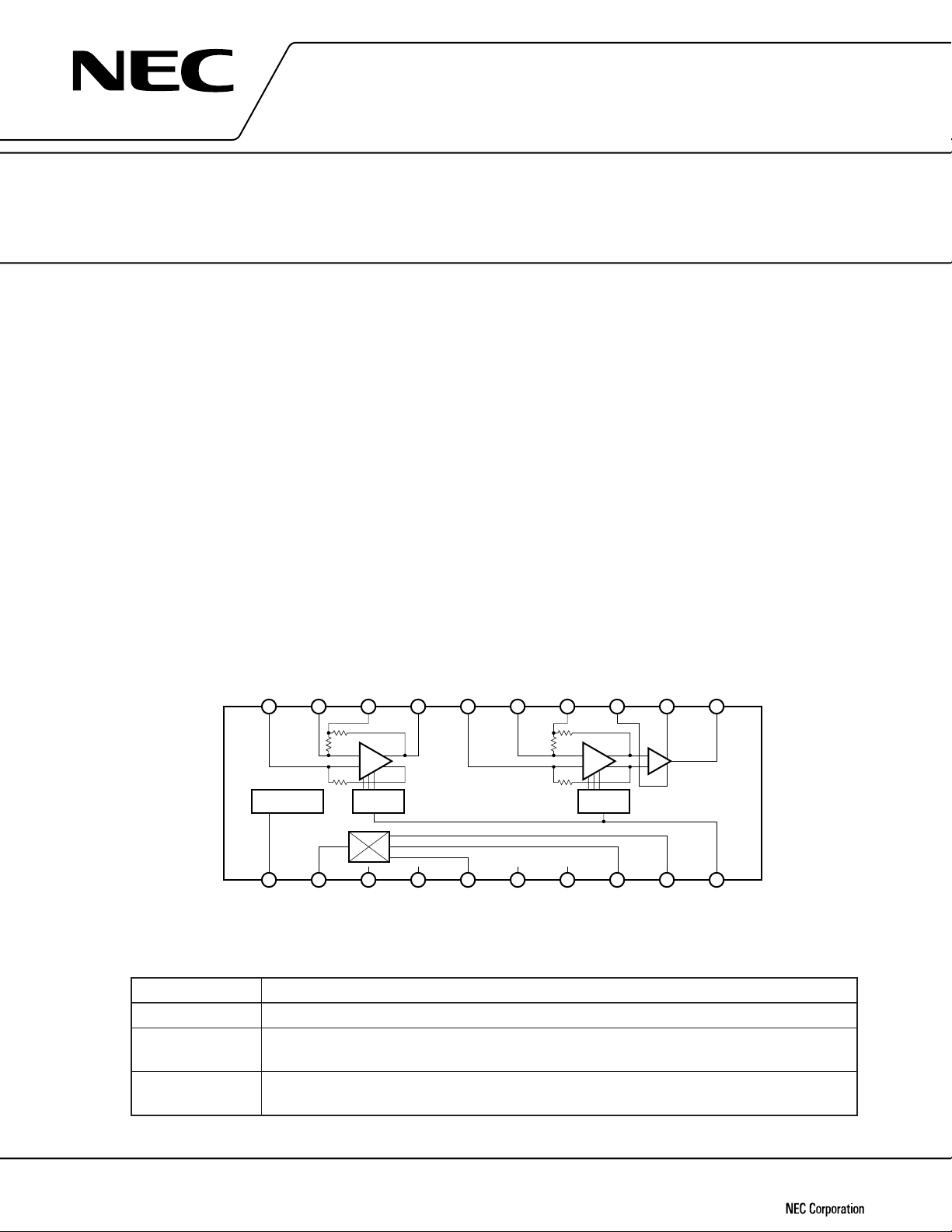
BLOCK DIAGRAM
BYPASS1
Power ON/OFF
IF1 IN19BYPASS218IF1 OUT17BYPASS416IF2 IN15BYPASS3
20
IF Amp 1
RSSI
2nd MIXER
1 1023456789
PD
LO IN
GND(IF) GND(MIX) MIX IN2MIX IN1
ORDERING INFORMATION
Part Number Package
µ
PC8002GR 20-pin plastic shrink SOP (225 mil)
µ
PC8002GR-E1 20-pin plastic shrink SOP (225 mil)
Embossed carrier taping (pin 1 is tape unwinding direction)
µ
PC8002GR-E2 20-pin plastic shrink SOP (225 mil)
Embossed carrier taping (pin 1 is tape winding direction)
14
GND
(IF OUT)
13
IF Amp 2
RSSI
VCC
(IF OUT)
12
Output Stage
IF2 OUT
11
RSSI OUTMIX OUT VCC (IF) VCC (MIX)
The information in this document is subject to change without notice.
Document No. S10717EJ2V0DS00 (2nd edition)
Date Published March 1997 N
Printed in Japan
©
1997

Application Circuit Example 1 (Using 2 BPFs)
V
CC
PD
1
BYPASS1
20
1000 pF
µ
PC8002
BPF
(MURATA)
CFEC10.7MK1
Lo OSC
1st Mixer
V
CC
1000 pF
V
CC
1000 pF
470 pF
470 pF
µ
1 F
1 F
µ
MIX OUT
2
V
3
V
4
LO IN
5
GND (IF)
6
GND (MIX)
7
MIX IN1
8
CC
CC
(IF)
(MIX)
IF1 IN
BYPASS2
IF1 OUT
BYPASS4
IF2 IN
BYPASS3
GND (IF OUT)
19
18
17
16
15
14
13
1000 pF
0.01 F
µ
0.01 F
µ
BPF
(MURATA)
CFEC10.7MK1
470 pF
9
MIX IN2
CC
(IF OUT)
V
12
1000 pF
ADC
10
RSSI OUT
IF2 OUT
11
Caution Ensure that the pin voltage does not exceed the power supply voltage.
Remark The V
CC pass capacitors (1
µ
F, 1000 pF) should be located close to the respective VCC pins.
Chip laminated ceramic capacitors (MURATA GRM36 or equivalent) should be used.
2
1 F
µ
V
CC
DEM
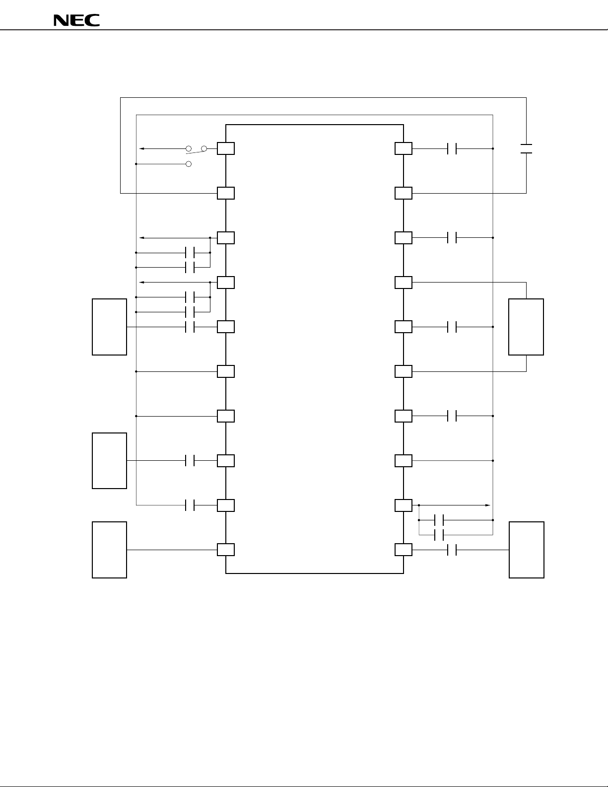
Application Circuit Example 2 (Using 1 BPF)
µ
PC8002
Lo OSC
V
CC
V
CC
1 F
1000 pF
V
CC
1 F
1000 pF
470 pF
1
2
3
PD
MIX OUT
CC
(IF)
V
BYPASS1
IF1 IN
BYPASS2
20
19
18
1000 pF
1000 pF
330 pF
µ
CC
(MIX)
V
4
IF1 OUT
17
µ
LO IN
5
GND (IF)
6
GND (MIX)
7
BYPASS4
BYPASS3
IF2 IN
16
15
14
0.01 F
µ
0.01 F
µ
BPF
(MURATA)
CFEC10.7MK1
1st Mixer
ADC
470 pF
470 pF
8
9
10
MIX IN1
MIX IN2
RSSI OUT
GND (IF OUT)
CC
(IF OUT)
V
IF2 OUT
13
12
1000 pF
11
µ
1 F
Cautions 1. Ensure that the pin voltage does not exceed the power supply voltage.
2. With this application circuit, confirm that there is not problem with interfering wave
characteristics.
Remark The V
CC pass capacitors (1
µ
F, 1000 pF) should be located close to the respective VCC pins.
Chip laminated ceramic capacitors (MURATA GRM36 or equivalent) should be used.
V
CC
DEM
3
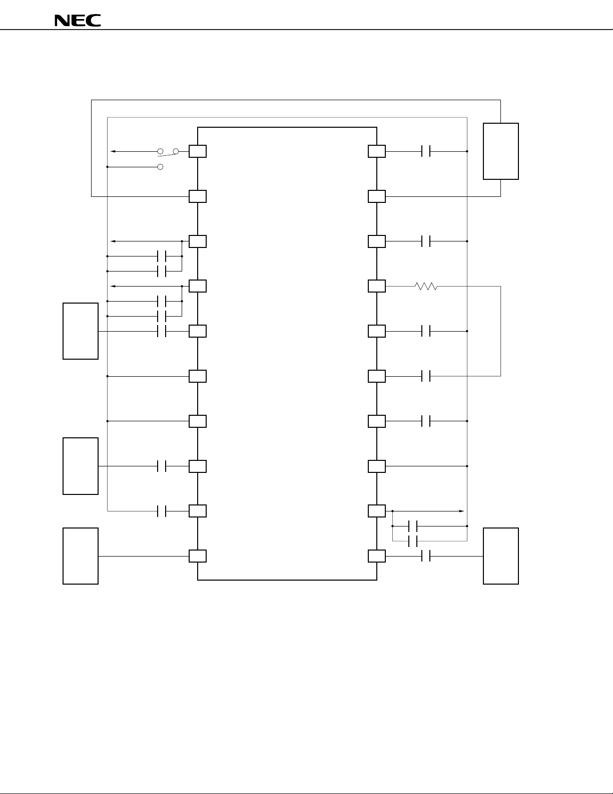
Application Circuit Example 3 (Using 1 BPF)
V
CC
PD
1
BYPASS1
20
1000 pF
µ
PC8002
BPF
(MURATA)
CFEC10.7MK1
Lo OSC
1st Mixer
V
CC
1000 pF
V
CC
1000 pF
470 pF
470 pF
µ
1 F
1 F
µ
MIX OUT
2
V
3
V
4
LO IN
5
GND (IF)
6
GND (MIX)
7
MIX IN1
8
CC
(IF)
CC
(MIX)
IF1 IN
BYPASS2
IF1 OUT
BYPASS4
IF2 IN
BYPASS3
GND (IF OUT)
19
18
17
16
15
14
13
1000 pF
390 Ω
µ
0.01 F
1000 pF
0.01 F
µ
V
1 F
µ
CC
ADC
470 pF
9
10
MIX IN2
RSSI OUT
CC
(IF OUT)
V
IF2 OUT
12
1000 pF
11
Cautions 1. With this application circuit, good interfering wave characteristics are obtained with a single
BPF. However, there is a drop in sensitivity.
2. Ensure that the pin voltage does not exceed the power supply voltage.
Remark The V
CC pass capacitors (1
µ
F, 1000 pF) should be located close to the respective VCC pins.
Chip laminated ceramic capacitors (MURATA GRM36 or equivalent) should be used.
4
DEM
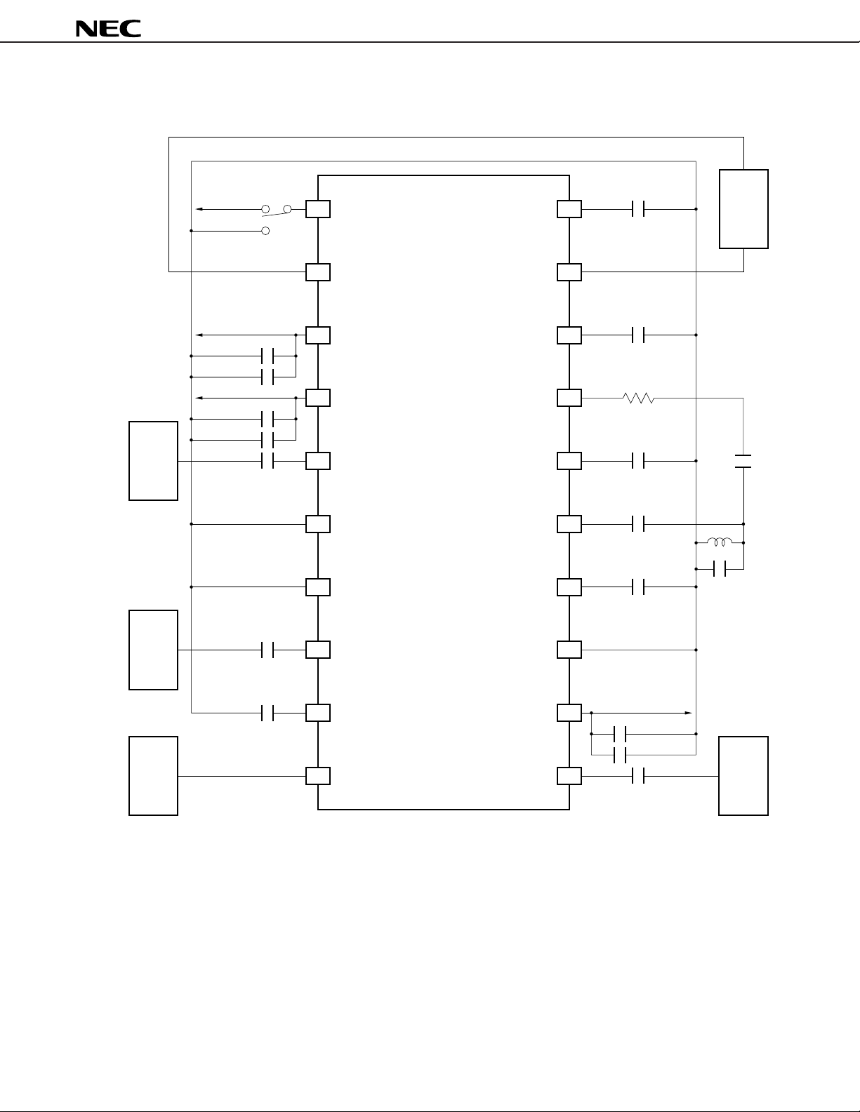
Application Circuit Example 4 (Using 1 BPF)
V
Lo OSC
CC
V
CC
1000 pF
V
CC
1000 pF
470 pF
1 F
µ
1 F
µ
1
2
3
4
5
PD
MIX OUT
CC
(IF)
V
V
CC
(MIX)
LO IN
BYPASS1
IF1 IN
BYPASS2
IF1 OUT
BYPASS4
20
19
18
17
16
1000 pF
1000 pF
390 Ω
µ
0.01 F
µ
PC8002
BPF
(MURATA)
CFEC10.7MK1
1000 pF
GND (IF)
1st Mixer
ADC
470 pF
470 pF
6
7
8
9
10
GND (MIX)
MIX IN1
MIX IN2
RSSI OUT
BYPASS3
GND (IF OUT)
CC
(IF OUT)
V
IF2 OUT
IF2 IN
15
14
13
12
1000 pF
11
µ
1 F
1000 pF
µ
0.01 F
V
CC
µ
1.5 H
150 pF
DEM
Cautions 1. With this application circuit, good interfering wave characteristics are obtained with a single
BPF (and sensitivity is better than in Application Circuit Example 3).
2. Ensure that the pin voltage does not exceed the power supply voltage.
Remark The V
Chip laminated ceramic capacitors (MURATA GRM36 or equivalent) and a chip coil (MURATA LQHIN
or equivalent) should be used.
CC pass capacitors (1
µ
F, 1000 pF) should be located close to the respective VCC pins.
5

µ
PC8002
CONTENTS
1. PIN CONFIGURATION AND PIN FUNCTIONS....................................................................................7
2. INPUT/OUTPUT EQUIV ALENT CIRCUIT DIAGRAMS ........................................................................9
3. ELECTRICAL SPECIFICATIONS .......................................................................................................10
4. CHARACTERISTIC DIAGRAMS ........................................................................................................13
5. LEVEL DIAGRAMS.............................................................................................................................17
6. TEST METHODS ................................................................................................................................18
7. TEST CIRCUIT EXAMPLES ...............................................................................................................19
8. EV ALUATION BOARD MOUNTING EXAMPLE .................................................................................25
9. WIRING P A TTERN CAPACITANCE DIAGRAM (REFERENCE) ........................................................28
10. P ACKAGE DRA WINGS.......................................................................................................................29
11. RECOMMENDED SOLDERING CONDITIONS..................................................................................30
6
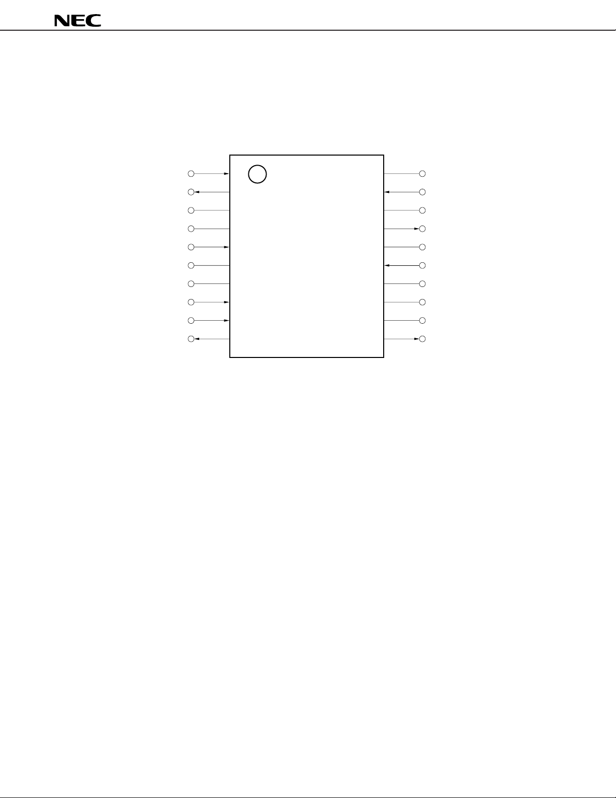
1. PIN CONFIGURATION AND PIN FUNCTIONS
(1) Pin Configuration (Top View)
• 20-pin plastic shrink SOP (225 mil)
µ
PC8002
PD
MIX OUT
V
CC
(IF)
CC
(MIX)
V
LO IN
GND (IF)
GND (MIX)
MIX IN1
MIX IN2
RSSI OUT
1
2
3
4
5
6
7
8
9
10
20
19
18
17
16
15
14
13
12
11
Pin Names
BYPASS1-BYPASS4 : Bypass
GND (IF) : Ground (Intermediate Frequency Amp.)
GND (IF OUT) : Ground (Intermediate Frequency Amp. Output)
GND (MIX) : Ground (Mixer)
IF1 IN, IF2 IN : Intermediate Frequency Amp. Input
IF1 OUT, IF2 OUT : Intermediate Frequency Amp. Output
LO IN : Local Input
MIX IN1, MIX IN2 : Mixer Input
MIX OUT : Mixer Output
PD : Power Down
RSSI OUT : Received Signal Strength Indicator Output
CC (IF) : Power Supply (Intermediate Frequency Amp.)
V
VCC (IF OUT) : Power Supply (Intermediate Frequency Amp. Output)
VCC (MIX) : Power Supply (Mixer)
BYPASS1
IF1 IN
BYPASS2
IF1 OUT
BYPASS4
IF2 IN
BYPASS3
GND (IF OUT)
CC
(IF OUT)
V
IF2 OUT
7

(2) Pin Functions
No. Pin Name I/O Function
1 PD I Power on/off control signal input
2 MIX OUT O Mixer output
3VCC (IF) – IF amplifier and RSSI power supply pin
4VCC (MIX) – Mixer power supply pin
5 LO IN I Local input
6 GND (IF) – IF amplifier and RSSI ground pin
7 GND (MIX) – Mixer ground pin
8 MIX IN1 I Mixer input
9 MIX IN2 I Filter capacitor connection
10 RSSI OUT O RSSI output
11 IF2 OUT O IF amplifier 2 output
12 VCC (IF OUT) – IF amplifier output stage power supply pin
13 GND (IF OUT) – IF amplifier output stage ground pin
14 BYPASS3 – Filter capacitor connection (IF2 side)
15 IF2 IN I IF amplifier 2 input
16 BYPASS4 – Filter capacitor connection (IF2 side)
17 IF1 OUT O IF amplifier 1 output
18 BYPASS2 – Filter capacitor connection (IF1 side)
19 IF1 IN I IF amplifier 1 input
20 BYPASS1 – Filter capacitor connection (IF1 side)
µ
PC8002
8
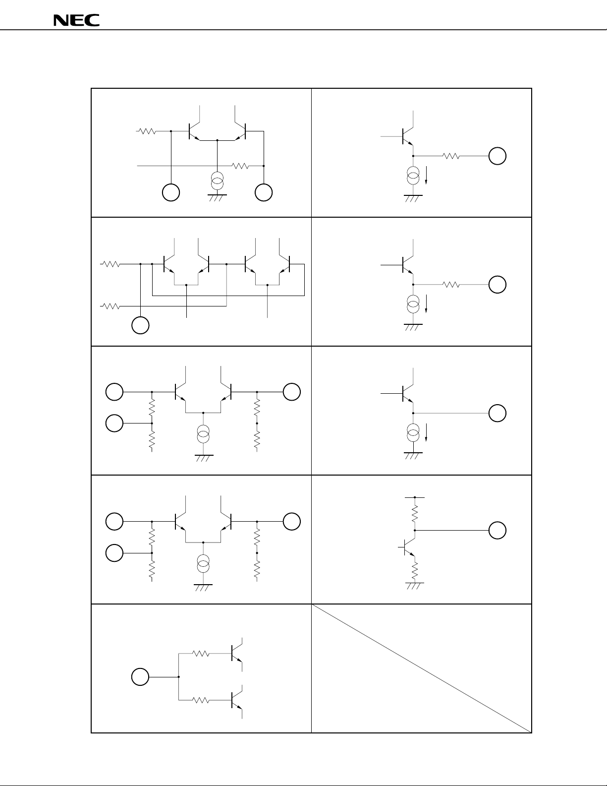
2. INPUT/OUTPUT EQUIVALENT CIRCUIT DIAGRAMS
µ
PC8002
Mixer Input
1 kΩ
Local Input
1 kΩ
1 kΩ
5
IF Amplifier 1 Input
Mixer Output
276 Ω
1 kΩ
700 A
µ
8
9
2
IF Amplifier 1 Output
207 Ω
µ
250 A
17
IF Amplifier 2 Output
19
330 Ω
18
14.9 kΩ
IF Amplifier 2 Input
15
330 Ω
14
11.8 kΩ
Power On/Off Input
1
50 kΩ
150 kΩ
330 Ω
14.9 kΩ
330 Ω
11.8 kΩ
20
16
RSSI Output
V
CC
32 kΩ
2 kΩ
290 A
µ
11
10
9
µ
PC8002
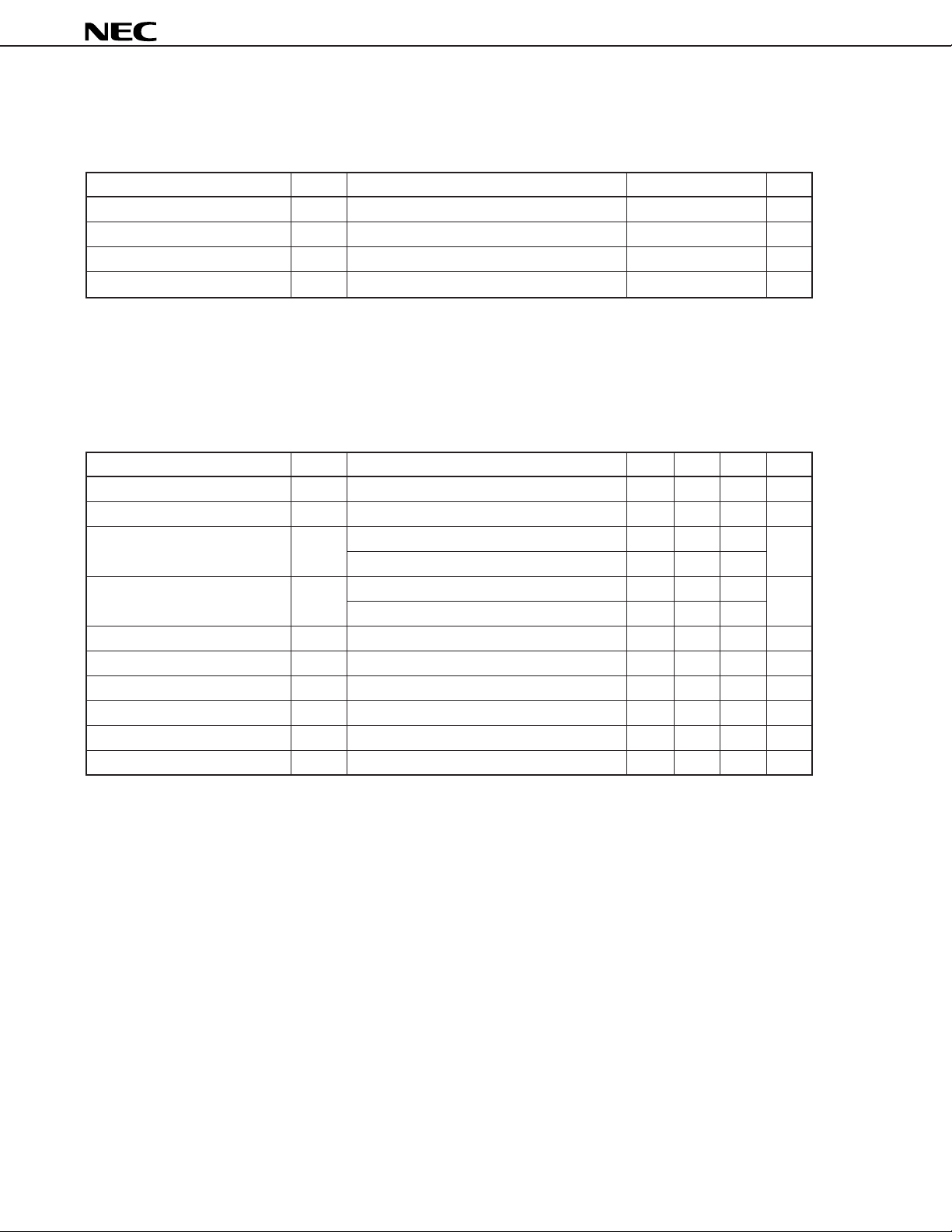
3. ELECTRICAL SPECIFICATIONS
Absolute Maximum Ratings (TA = 25 °C)
Parameter Symbol Test Condition Rating Unit
Power supply voltage VCC 7V
Total power dissipation PT TA = 85 °C 120 mW
Storage temperature Tstg –40 to +125 °C
Pin voltage VPIN VCC+0.2 V
Caution Product quality may suffer if the absolute rating is exceeded for any parameter, even momentarily.
In other words, an absolute maximum rating is a value at which the possibility of physical damage
to the product cannot be ruled out. Care must therefore be taken to ensure that the these ratings
are not exceeded during use of the product.
Recommended Operating Ratings (T
Parameter Symbol Test Condition MIN. TYP. MAX. Unit
Power supply voltage VCC 2.7 3.0 5.5 V
Operating ambient temperature TA –30 +25 +85 °C
Mixer input level VMIX 50 Ω resistance termination –98 –18 dBm
Local input level VLOC 50 Ω resistance termination –5 +5 dBm
IF amplifier input level VIF –99 –14 dBm
Mixer input frequency fMIX 250 500 MHz
Mixer output frequency fOM 8 10.7 12 MHz
IF amplifier input frequency fIF 8 10.7 12 MHz
RSSI output load capacitance COI 10
IF2 output load capacitance COR 10
A = 25 °C) 0 dBm = 223.6 mVrms (at 50 Ω)
LC matching (reference value) –107 –27
LC matching (reference value) –20 –10
Note
Note
Note Includes all capacitances (board, pattern, etc.) applied to the pin.
pF
pF
10
 Loading...