NEC UPC2711TB-E3, UPC2711TB, UPC2711T-E3, UPC2711T Datasheet

DATA SHEET
DATA SHEET
BIPOLAR ANALOG INTEGRATED CIRCUIT
PPPP
2.9 GHz WIDE BAND AMPLIFIER
SILICON BIPOLAR MONOLITHIC INTEGRATED CIRCUIT
FEATURES
• High power gain : 13 dB TYP. @ f = 1 GHz
• Excellent frequency response: 2.9 GHz TYP. @ 3 dB down below the gain at 0.1 GHz
• Noise figure : 5 dB
• Single supply voltage : 5 V
• Input and output matching : 50
• Super small package : 6 pin mini mold
:
PC2711T
ORDERING INFORMATION
PART NUMBER PACKAGE SUPPLYING FORM
P
PC2711T-E3 6 pin mini mold Embossed tape 8 mm wide.
Pin 1, 2, 3 face to perforation side of the tape.
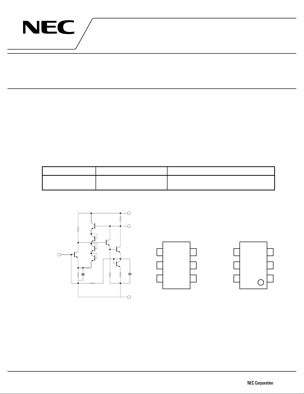
EQUIVALENT CIRCUIT PIN CONNECTIONS
VCC
OUT
(Top View)
IN
GND
3
2
1
4
1. INPUT
5
2. GND
3. GND
4. OUTPUT
6
C 1 G
5. GND
CC
6. V
(Bottom View)
4
5
6
3
2
1
Document No. P12428EJ2V0DS00 (2nd edition)
(Previous No. IC-2948)
Date Published March 1997 N
Printed in Japan
Caution: Electro-static sensitive devices
1993©

ABSOLUTE MAXIMUM RATINGS (TA = +25 °C)
PPPP
PC2711T
CC
CC
opt
stg
6V
30 mA
D
in
280
*
40 to +85 °C
ð
55 to +150 °C
ð
+10 dBm
mW
Supply Voltage V
Total Circuit Current I
Power Dissipation P
Operating Temperature T
Storage Temperature T
Input Power P
Mounted on 50 u 50 u 1.6 mm epoxy glass PWB (TA = +85 °C)
*
RECOMMENDED OPERATING CONDITIONS
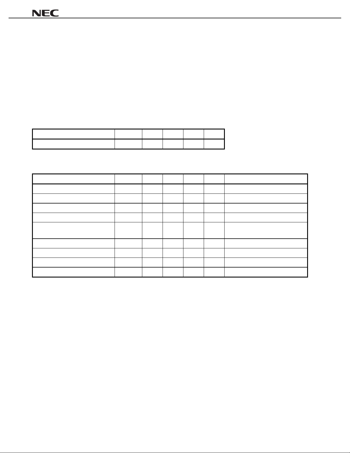
PARAMETER SYMBOL MIN. TYP. MAX. UNIT
'
CC
CC
P
O(sat)
U
out
G
4.5 5.0 5.5 V
)
::::
9 12 15 mA No signal
11 13 16.5 dB f = 1 GHz
ð2 +1 dBm f = 1 GHz, Pin = 0 dBm
2.7 2.9 GHz 3 dB down below flat gain
f = 0.1 GHz
in
P
20 25 dB f = 1 GHz
9 12 dB f = 1 GHz
±0.8 dB f = 0.1 to 2.5 GHz
Supply Voltage V
ELECTRICAL CHARACTERISTICS (TA = +25 °C, VCC = 5 V, ZS = ZL = 50
PARAMETERS SYMBOL MIN. TYP. MAX. UNIT TEST CONDITIONS
Circuit Current I
Power Gain G
Maximum Output Level P
Noise Figure NF 5 6.5 dB f = 1 GHz
Upper Limit Operating Frequency f
Isolation ISL 25 30 dB f = 1 GHz
Input Return Loss RL
Output Return Loss RL
Gain Flatness
2

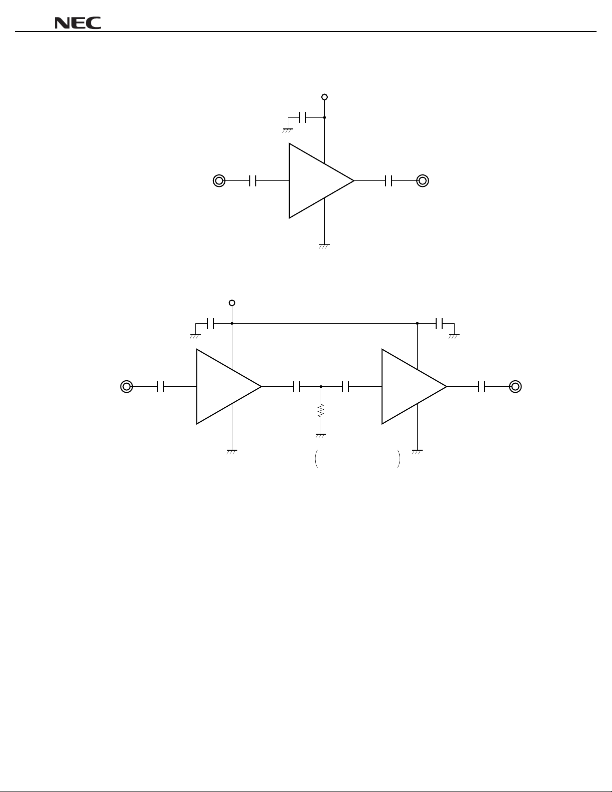
TEST CIRCUIT
C
50 Ω
1
IN
1 000 pF
EXAMPLE OF APPLICATION CIRCUIT
V
CC
1 000 pF
C
1
PPPP
PC2711T
V
CC
3
6
C
2
4
50 Ω
OUT
1 000 pF
2, 3, 5
IN
50 Ω
1
C
1 000 pF
1 000 pF
C
1
3
6
C
4
4
1 000 pF
C
1 000 pF
R
1
5
1
6
1 000 pF
C
6
4
2
C
1 000 pF
50 Ω
OUT
50 to 200 Ω
2, 3, 5
2, 3, 5
To stabilize operation,
1
, C
please connect R
5
The application circuits and their parameters are for reference only and are not intended for use in actual design-ins.
Capacitors for VCC, input and output pins
1 000 pF capacitors are recommendable as bypass capacitor for V
CC
pin and coupling capacitors for input/output
pins.
Bypass capacitor for VCC pin is intended to minimize VCC pin’s ground impedance. Therefore, stable bias can be
supplied against VCC fluctuation.
Coupling capacitors for input/output pins are intended to minimize RF serial impedance and cut DC.
To get flat gain from 100 MHz up, 1 000 pF capacitors are assembled on the test circuit. [Actually, 1 000 pF
capacitors give flat gain at least 10 MHz. In the case of under 10 MHz operation, increase the value of coupling
capacitor such as 2 200 pF. Because the coupling capacitors are determined by the equation of C = 1/(2 S fZs).]
3

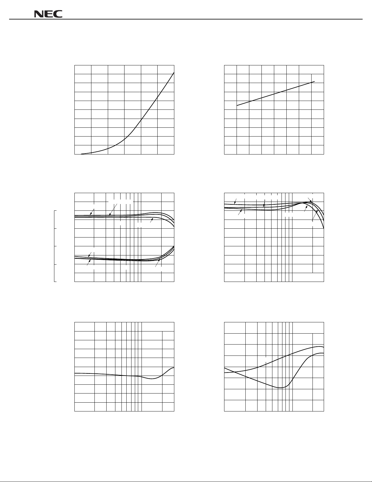
TYPICAL CHARACTERISTICS (TA = 25 °C)
PPPP
PC2711T
20
18
16
14
12
10
8
6
ICC – Circuit Current – mA
4
2
0 123456
20
8
7
6
15
10
5
CIRCUIT CURRENT vs. SUPPLY VOLTAGE
V
CC – Supply Voltage – V
NOISE FIGURE AND INSERTION
POWER GAIN vs. FREQUENCY
VCC = 5.5 V
VCC = 5.5 V
VCC = 5.0 V
G
P
VCC = 4.5 V
CIRCUIT CURRENT vs.
20
18
16
14
12
10
8
6
ICC – Circuit Current – mA
4
2
0
15
10
OPERATING TEMPERATURE
–40 –20 40 60 80
T
opt – Operating Temperature – °C
INSERTION POWER GAIN vs. FREQUENCY
TA = –40 °C
TA = +85 °C
0–60 20 100
TA = +25 °C
TA = –40 °C
VCC = 5.0 V
TA = +85 °C
TA = +25 °C
5
NF – Noise Figure – dB
4
0
VCC = 4.5 V
GP – Insertion Power Gain – dB
–5
0.1 0.3 1.0 3.0
0
–10
–20
–30
ISL – Isolation – dB
–40
–50
0.1
NF
f – Frequency – GHz
ISOLATION vs. FREQUENCY
0.3 1.0 3.0
f – Frequency – GHz
VCC = 5.0 V
V
CC = 5.0 V
GP – Insertion Power Gain – dB
CC = 5.0 V
5
0.1 0.3 1.0 3.0
f – Frequency – GHz
INPUT RETURN LOSS, OUTPUT
0
–10
–20
–30
out – Output Return Loss – dB
RL
RLin – Input Return Loss – dB
–40
RETURN LOSS vs. FREQUENCY
RLout
0.1
0.3 1.0 3.0
f – Frequency – GHz
V
VCC = 5.0 V
RLin
4
 Loading...